chapteriv noiseanddistortion - rf toolboxrftoolbox.dtu.dk/book/ch4.pdf ·...
TRANSCRIPT

Class Notes, 31415 RF-Communication Circuits
Chapter IV
NOISE and DISTORTION
Jens Vidkjær
NB 232

ii

Contents
IV Noise and Distortion . . . . . . . . . . . . . . . . . . . . . . . . . . . . . . . . . . . . . . . . . . . . 1IV-1 Sources and Basic Properties of Electrical Noise . . . . . . . . . . . . . . . . . 2
Thermal Noise . . . . . . . . . . . . . . . . . . . . . . . . . . . . . . . . . . . . . . 2Example IV-1-1 (noise in a RC circuit, noise bandwidth) . . . 4
Shot Noise . . . . . . . . . . . . . . . . . . . . . . . . . . . . . . . . . . . . . . . . . 6Flicker or 1/f Noise . . . . . . . . . . . . . . . . . . . . . . . . . . . . . . . . . . . 8Other Noise Sources in Electronics . . . . . . . . . . . . . . . . . . . . . . . . 10Characterizing and Combining Noise Sources . . . . . . . . . . . . . . . . . 11Man-Made Noise . . . . . . . . . . . . . . . . . . . . . . . . . . . . . . . . . . . . . 13
IV-2 Noise in Semiconductor Devices . . . . . . . . . . . . . . . . . . . . . . . . . . . . 15Noise in Diodes . . . . . . . . . . . . . . . . . . . . . . . . . . . . . . . . . . . . . . 15Noise in Bipolar Transistors . . . . . . . . . . . . . . . . . . . . . . . . . . . . . 17
Example IV-2-1 ( minimum noise in bipolar transistors ) . . . 18Noise in Field Effect Transistors . . . . . . . . . . . . . . . . . . . . . . . . . . 22
IV-3 Noise Characterization of Two-Ports . . . . . . . . . . . . . . . . . . . . . . . . . 25Noise Figure . . . . . . . . . . . . . . . . . . . . . . . . . . . . . . . . . . . . . . . . 25
Example IV-3-1 ( noise figure measurement) . . . . . . . . . . . 28Noise Temperature of Two-Ports . . . . . . . . . . . . . . . . . . . . . . . . . . 29Noise in Cascaded Two-Ports . . . . . . . . . . . . . . . . . . . . . . . . . . . . 30
Example IV-3-2 ( link budget ) . . . . . . . . . . . . . . . . . . . . . 31Noise Representation in Two-Ports . . . . . . . . . . . . . . . . . . . . . . . . 33Minimum Noise Conditions . . . . . . . . . . . . . . . . . . . . . . . . . . . . . 36Constant Noise Figure Circles . . . . . . . . . . . . . . . . . . . . . . . . . . . . 37
Example IV-3-3 ( noise figure circles in Y-plane ) . . . . . . . 39Example IV-3-4 ( noise figure circles in Smith chart ) . . . . . 42
IV-4 Distortion in Almost Linear Circuits . . . . . . . . . . . . . . . . . . . . . . . . . . 47Single Signal Distortions . . . . . . . . . . . . . . . . . . . . . . . . . . . . . . . 48Distortions with Two Signals . . . . . . . . . . . . . . . . . . . . . . . . . . . . 52Intercept Points . . . . . . . . . . . . . . . . . . . . . . . . . . . . . . . . . . . . . . 56Sensitivity and Dynamic Range . . . . . . . . . . . . . . . . . . . . . . . . . . . 59
Problems . . . . . . . . . . . . . . . . . . . . . . . . . . . . . . . . . . . . . . . . . . . . . . . . 62References and Further Reading . . . . . . . . . . . . . . . . . . . . . . . . . . . . . . . . 66
Index . . . . . . . . . . . . . . . . . . . . . . . . . . . . . . . . . . . . . . . . . . . . . . . . . . . . . . . . . 69
iii

iv

1
IV Noise and Distortion
Linear amplification for a wide range of signal levels is crucial in many RF applica-tions. Electronic circuits may be designed to show linearity over large operating ranges, buteventually the condition ceases at both high and low drive levels as demonstrated by thetypical amplifier characteristic in Fig.1.
When at low levels the output flattens to constancy regardless of input, we havereached the so-called noise floor. Its major causes are thermal motions and quantizised currentflows in the circuit components, which add a random fluctuation to the deterministic outputsignals. When noise and signal become equal in size, we are close to the borderline belowwhich the output is useless. It is a common design challenge to push the noise floor to anacceptable minimum in a given application, and it is one of the major objectives of the presentsection to provide the background and present techniques for doing so.
In the opposite range of input drives the amplifier performance degenerates due tononlinearities in the circuit, commonly introduced by the large signal operation of transistorsor other electron devices. At the ultimate edge the output may saturate to constancy but inmost application the limit for acceptable performance is reached long before that. There aremany occasions where we highly benefit from nonlinear operation of electronic circuits butpresently we focus on failures that arise when linearity is expected. Transmission of a signalthrough a nonlinear device is accompanied by formation of deterministic distortion compo-nents at frequencies which differs from the input signal frequencies. Filtering may removesome of these new components, known as spurious responses, but others are so close to theoriginal ones that they seriously influence the signal processing that succeeds amplification,detection for instance. We shall consider various forms of nonlinear distortions and theircharacterization in the last section of this chapter.
Fig.1 Typical input-output characteristic of an amplifier designed for linear applications.
J.Vidkjær

2 Noise and Distortion
IV-1 Sources and Basic Properties of Electrical Noise
A voltage or current carrying a signal includes in practice both the desired determin-istic signal and disturbing components, which again may be either deterministic or random.The latter encompasses terms that are completely unavoidable on basis of fundamentalphysical principles, and they are always referred to as noise. Solving practical problem, more-over, other non-ideal contributions may be included under the noise term, particularly if thestatistical means and properties that apply to physical noise remain usable. The basic originsand properties of electrical noise are presented in this first section with the aim of providinga foundation for our subsequent discussion of noise in electronic devices and circuits.
Thermal Noise
Thermal motion of the electrons in a resistor causes a fluctuating noise voltage acrossthe terminals. The voltage has Gaussian distribution around a mean value of zero. If theresistor is in thermal equilibrium with its surroundings at temperature T [K], the two-sidedspectral density of the mean squared noise voltage is given by,
The first frequency dependent expression is included to indicate that there is a natural upper
(1)
frequency roll-off in spectral density, even though it suffices for most practical purposes touse the last - frequency independent - approximation. Around room temperature 300 K wehave kT/h=6.44 THz, so here it is the bandwidth of circuit embodying the resistor that imposerestrictions on the resultant noise. In a frequency band of Δf Hz around any frequencyω0=2πf0 fairly below the kT/h bound, thermal noise provides a fluctuation voltage vn that stillhas zero mean value and a variance, i.e. mean squared value, given by1
(2)
1 ) The overline notation has a long tradition in noise literature for both time averaginglike <vn
2> in common notation or statistical averaging - expectation - like E[vn2].
Most noise processes we consider are ergodic with equal time and ensemble averagesand the overline notation is maintained below unless it leads to ambiguity.
J.Vidkjær

3IV-1 Sources and Basic Properties of Electrical Noise
Fig.2 Double-sided power spectral density of thermal noise from a resistor. The meansquared voltage from frequency interval Δf is the hatched area divided by 2π.
Fig.3 Circuit schematic representations of thermal noise from a resistor. The square rootsare often omitted for clarity although the noise generators still represent RMS (rootmean square) voltages or currents.
Incorporating thermal noise from a resistor in a circuit diagram is often done asshown by Fig.3(b). The noise is accounted for separately by the RMS voltage generator andthe resistor R is assumed noiseless. Translated to the Norton equivalent form in Fig.3(c), thecorresponding short-circuit noise current is given by
where conductance G equals 1/R. It is superfluous in most cases to orient the noise voltage
(3)
or current generators as it is done in the figures. On the other hand this makes no harm, sothe orientations are maintained since we later shall consider situations that requires signs.Regarding equivalent circuits that incorporates noise sources of the types above, there is a tacitassumption that if we are going to measure a noise voltage, ideal filtering must precede theinstrument. Fig.4 shows the simplest case, where a resistor is the only circuit component.
Fig.4 Hypothetical setup for noise voltage measurement corresponding to Fig.3. Substi-tuting with practical filters Δf represents the so-called noise bandwidth.
J.Vidkjær

4 Noise and Distortion
The available noise power Nav from the equivalent circuits in Fig.3(b) and (c) is independentof the resistance value and given by,
Thermal noise is sometimes called Johnson noise after its discoverer. The physical
(4)
and mathematical descriptions were provided by Nyquist, who also proved that any electricalsystem in thermal equilibrium has an open circuit thermal noise voltage corresponding to thereal part of the impedance, equivalently a short-circuit current corresponding to the real partof the admittance. Both cases agree with the available power expression from Eq.(4).
It is assumed here that the frequency interval Δf is small enough to assume constancy of the
(5)
(6)
impedance or admittance across the interval, alternatively that Δf represents the so-called noisebandwidth, which is exemplified below. Cases that can be described by the method aboveinclude noise from magnetization losses in inductors and transformers, noise due to dielectricallosses in transmission lines, noise from the radiation and reception resistance in antennas,microphones or other transducers. For a more genuine discussion of these and many otherbasic topics, the reader should consult ref’s [1] and [2], which are collections of funda-mental papers on noise in electrical circuits.
Example IV-1-1 (noise in a RC circuit, noise bandwidth)
Consistency of the above results is demonstrated below by considering the RC
Fig.5 Calculation of RC circuit noise from (a), transfer function H(jω)=vno/En , and (b)directly from Eq.(5).
network in Fig.5(a). It has the output impedance
J.Vidkjær

5IV-1 Sources and Basic Properties of Electrical Noise
The mean-squared output noise voltage per unit bandwidth follows directly from Eq.(5),
(7)
A leading factor of two is required in the equation above to let Svo(ω) be a double-sided
(8)
spectrum. We shall see that the same result follows from the resistor noise representation inFig.5(a) where H(jω) is the transfer function from voltages En to voltage vno. This is a usualvoltage division, which in absolutely squared form provides
i.e. the same result as the one obtained by Eq.(8). Including all frequencies, it is furthermore
(9)
seen, that the total mean-squared voltage from a RC circuit is independent of the resistancevalue,
since the last definite integral is π/2. The noise output voltage is also the voltage across the
(10)
capacitor, which therefore holds a thermal noise mean energy of size
This result shows agreement with classic statistical thermodynamics. A system in thermal
(11)
equilibrium with its surroundings at an absolute temperature T has an energy of ½kT perdegree of freedom, i.e. number of state variables required to describe the system. The RCcircuit needs only one - the capacitor voltage.
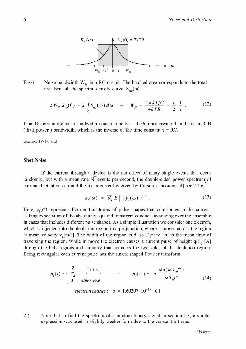
The so-called noise bandwidth is illustrated by Fig.6 for the RC circuit. It is thebandwidth that provides the same available noise power from a uniform distribution at peaklevel as the power actually available from the entire, frequency dependent distribution. Thenoise-bandwidth WN spans the interval from -WN to WN, so the hatched rectangle has an areaequal to the area beneath the actual spectral density curve. Using the result from Eq.(10), thenoise-bandwidth in radians per second becomes
J.Vidkjær
6 Noise and Distortion
In an RC circuit the noise bandwidth is seen to be ½π = 1.56 times greater than the usual 3dB
Fig.6 Noise bandwidth WN in a RC-circuit. The hatched area corresponds to the totalarea beneath the spectral density curve, Sno(ω).
(12)
( half power ) bandwidth, which is the inverse of the time constant τ = RC.
Example IV-1-1 end
Shot Noise
If the current through a device is the net effect of many single events that occurrandomly, but with a mean rate ⎯NI events per second, the double-sided power spectrum ofcurrent fluctuations around the mean current is given by Carson’s theorem, [4] sec.2.2.c,2
Here, pI(ω) represents Fourier transforms of pulse shapes that contributes to the current.
(13)
Taking expectation of the absolutely squared transform conducts averaging over the ensemblein cases that includes different pulse shapes. As a simple illustration we consider one electron,which is injected into the depletion region in a pn-junction, where it moves across the regionat mean velocity ve[m/s]. The width of the region is d, so Td=d/ve [s] is the mean time oftraversing the region. While in move the electron causes a current pulse of height q/Td [A]through the bulk-regions and circuitry that connects the two sides of the depletion region.Being rectangular each current pulse has the sinx/x shaped Fourier transform
(14)
2 ) Note that to find the spectrum of a random binary signal in section I-3, a similarexpression was used in slightly weaker form due to the constant bit-rate.
J.Vidkjær

7IV-1 Sources and Basic Properties of Electrical Noise
A train of electron pulses sums up to the DC current I=q⎯NI. Substituting I into Eq(13), the
Fig.7 Train of pulses, each representing the transition of one electron across the deple-tion region in a pn-junction.
doublesided spectrum for current fluctuations becomes
Thus, the total mean squared noise current from the fluctuations in a frequency band Δf
(15)
around ω0 = 2πf0 is given by
The last, approximated result is called Schottky’s theorem. It represents the limit where Td→0,
(16)
so each current contribution is an impulse - a shot - of weight q and a flat spectrum inconcordance with the 1/Td frequency bound for the approximation. The frequency independentsimplification suffices for most practical application of devices that exhibits shot noise, forinstance Schottky barrier and pn junction diodes or bipolar transistors where the time carriersare in drift across depletion regions commonly are considerably shorter than the transit timethrough neutral bulk regions [3].
Fig.8 Spectrum of a mean squared shot noise current. In a pn-junction T is the transittime of carriers across the depletion region.
J.Vidkjær

8 Noise and Distortion
Flicker or 1/f Noise
While the types of noise considered above were ascribed to specific and well underst-ood noise mechanism, the term flicker or 1/f noise is distinguished solely from the shape ofthe spectral density,
The numerator C depends commonly upon the device biasing, but it is independent of
(17)
frequency. This type of noise is observed in most electronic devices, passive as well as active,although the extent may vary by orders of magnitude between different types. Amongtransistors, MOSFET’s are in the high flicker noise end and BJT’s are in the low end.Considering resistors, bulk carbon and carbon film types are the noisiest while metal film orwirewound resistors have low flicker noise.
Fig.9 Spectrum including flicker noise for the mean squared noise voltage across a carbonresistor. I0 is the DC current through the resistor.
To exemplify flicker noise we start considering the noise voltage across a carbonresistor. In addition to the flat thermal noise spectrum we get an 1/f shaped contribution assketched in Fig.9. Observations show that the level of flicker noise is proportional to thesquare of the DC current through the resistor, an influence that may be understood if weassociate the 1/f noise with random resistance fluctuations δR around a mean value R0,
Applying DC current I0, the voltage across the resistor and especially the mean squared noise
(18)
voltage are given by
The spectrum of the mean squared voltage fluctuations originates here from a 1/f spectrum
(19)
in the mean squared resistance fluctuations. Note that the DC current only is required toobserve the noise but not for controlling the underlying mechanisms of resistance fluctuations.
J.Vidkjær

9IV-1 Sources and Basic Properties of Electrical Noise
Although flicker noise basically is a low frequency phenomenon, low frequencyparameter fluctuations might get substantial influence on RF circuit performances. Applyinga sinusoidal current Iccosωct in the carbon resistor case gives the voltage components
The last term holds the noise, but it is no longer a stationary random variable but a cyclo-
(20)
stationary one of period Tc=2π/ωc. The resultant power spectrum for the mean squared voltageis given by
The two first terms account for the sinusoidal carrier in v1. If SRf(ω) denotes the mean square
(21)
1/f shaped spectrum of the stationary random variable δR, the noise portion of the resultantspectrum is shifted in frequency to fringe the carrier. Suppose we have two signals representedby carriers Ic1 and the nearby but much smaller Ic2, which is the one we subsequently wantto separate by filtering and detect. From the above relationship and the sketch in Fig.10, wesee that the flicker noise induced by the large carrier may overwhelm the signal to be foundand the succeeding filtering becomes difficult. So despite its basic low-frequency outset,flicker noise may be critical also at RF frequencies.
Fig.10 Noise and signal components when two RF signals are inflicted by parameter flickernoise like resistance fluctuations in carbon resistors. Only the positive frequency partsfrom Eq.(21) are shown.
Flicker noise contribution to the mean squared noise voltage in a frequency intervalfrom fl to fu by the 1/f relationship gives
(22)
J.Vidkjær
10 Noise and Distortion
Both limits, fu→∞ or fl→0, make unrealistic advancements towards infinity. A closer look ondetails in the spectrum must therefore depart from 1/f in the limits. In the high end thespectrum must roll off faster than 1/f, for example like 1/f2 above a certain frequency fl.Correspondingly the spectrum must grow slower than 1/f when f goes towards zero. Aconstant spectrum below a certain frequency fl would be appropriate. For most practical noisecalculations we have commonly no detailed knowledge about these matters. If the bandwidthof interest spans the whole frequency range of flicker noise, a safe choice on the upper boundis to use fu above the limit frequency fa where thermal noise becomes dominant as indicatedby Fig.9. The low bound fl could be chosen so low that we are no longer willing to spent timeobserving consequences of the noise, alternatively 1/fl could be taken as the length of thelongest message that is processed separately in a communication system.
There are many physical origins of flicker noise in electronic components anddevices. The cause in resistors might be fluctuations in the mobility of the carriers that conveythe current. In semiconductors, flicker noise also accompanies the generation and recombina-tion process of free carriers. Often phenomena that deteriorate normal device performance, forinstance uncontrolled oxide traps and surface states in transistors, contribute dominantly toflicker noise. In new device types this noise may be excessive, but commonly it levels offwhen the corresponding technology matures. Flicker noise in semiconductor devices manifestsitself both directly as noise currents or voltages, but it also contributes to parameter fluctua-tions. The transconductance, for instance, might get an 1/f spectrum, so the modulatingproperty that was illuminated for bulk resistors by Eq.(21) and Fig.10 applies to transistorsas well. Consult refs. [1] and [4] chap.8 to gain more insight into the physics behind 1/fnoise. A discussion of common basic aspects of the flicker noise may be found in ref.[5].
Other Noise Sources in Electronics
The three noise types we have considered are far the most prominent in RF circuits.They are also typical from the point of view, that we have covered three basic forms, theunavoidable flat spectrum thermal noise, the bias current dependent shot noise with approxi-mately flat spectrum, and finally flicker noise whose dominant low-frequency spectrumtransforms to RF and smear out signal spectra. There are other types and sources of noise.Most of them can hardly be distinguished from the types above in experimental data. For thesame reason, noise models in circuit simulator programs are concentrated around our basictypes. If other sources are present in the circuit, they are taken into account by parameteradjustments. However, some specific noise contributions are so frequently referred to inliterature that they need a few comments.
Generation-recombination noise accompanies the random processes of generating andrecombining carriers in electronic devices. If one mechanism dominates the process, forinstance a well defined trap, the corresponding noise gets a spectrum of shape,
(23)
J.Vidkjær

11IV-1 Sources and Basic Properties of Electrical Noise
Here τ is the lifetime of carriers. Factor K depends typically on bias currents. It is seen thatthe high frequency asymptote decays with the square of frequency, so it is much steeper thanin flicker noise. However, many different processes of widely separated lifetimes are usuallyengaged in generation and recombination of carriers in semiconductor devices. Their jointeffect approximates the 1/f spectral density of flicker noise [4].
Burst noise is a special form of generation-recombination noise with spectral density
Fig.11 Typical time-domain burst noise waveshape
like Eq.(23). This noise is sorted out due to its characteristic wave shape like the one inFig.11, but the basic mechanisms of the pronounced jumps are not completely understood [4].Burst noise is sometime called popcorn noise after the sound the waveshape produces in aloudspeaker. Like flicker and other noise types with low-frequency spectral dominance, burstnoise gets significance in RF if it controls device parameter variations.
Avalanche noise follows the avalanche effect in reverse biased pn-junctions. If thefield is sufficiently high, free carriers may gain the energy that is necessary to produce newelectron hole pairs by impact ionization. The total current is still made by a sequence ofrandom events, so the noise is a shot noise of the type in Eq.(16). However, the current inthe noise expression under reverse bias is not the saturation current IS, which we might extractfrom the characteristic of the forward biased junction, but instead the actual and commonlymuch greater experimental reverse current that includes avalanching.
Characterizing and Combining Noise Sources
The power spectral density functions are the direct way of specifying a noise source,either Sv(ω) [V
2/Hz] for a voltage source or Si(ω) [A2/Hz] for a current source. Data sheets
give often the square root of twice the densities that are shown, for instance the functions
Assuming flat spectrum, we get the RMS voltage or current from the noise source by multi-
(24)
plying the Vn(f) or the In(f) function by the square root of the frequency interval or the noisebandwidth in the measurements.
Instead of the direct specification above, noise sources of any kind are sometimescompared to the idealized flat spectrum thermal noise from resistors, which was defined by
J.Vidkjær

12 Noise and Distortion
either Eq.(2) or Eq.(3) for voltage and current respectively. There are two approaches here.The first one requires that the noise source has an output impedance or admittance withpositive real part. An effective noise temperature Teff for the one-port is now defined as thetemperature that an impedance equal to the one-port impedance must have to give thermalnoise equal to the observed noise. If a one-port has impedance Z1(ω0) and mean squared noisevoltage or current equal to either v⎯21 or i⎯
21 in the frequency interval Δf around ω0, the noise
temperature becomes
(25)
Another way of characterizing a noise source is to specify the resistance Rn or theconductance Gn that provide thermal noise equal to the observed source. This is particularlyuseful when the source is given solely in the form of either a RMS voltage or a RMS currentgenerator at a given temperature. Rn and Gn are called the noise resistance and the noiseconductance respectively. If the observed noise in frequency interval Δf is either v⎯21 or i⎯
21,
the corresponding noise resistance or conductance are
It should be emphasized that Rn and Gn are noise level parameters, which are not required to
(26)
be recognizable as resistors or conductances in an equivalent circuit, although this will be thecase, if the noise is thermal and the temperature has been agreed upon. The temperature isoften the reference temperature of 290 [K], which is a part of the noise figure definition fortwo-ports to be discussed below in section IV-3 on page 25.
The combined effect of two series connected noise voltage sources - two paralleled
Fig.12 Combining uncorrelated noise sources. The mean square of the resultant voltageor current is the sum of the two original mean squared quantities.
noise current sources behave similarly - must be calculated on a mean-squared basis to yield
Here ρ is a correlation coefficient between the two sources. With time averaging it is defined
(27)
J.Vidkjær

13IV-1 Sources and Basic Properties of Electrical Noise
This coefficient is confined to the interval [-1 ≤ρ≤1].
(28)
Uncorrelated noise sources have a zero-valued correlation coefficient, so the meansquare of the result becomes the sum of mean squares from the two original sources asindicated by Fig.12. Imagining that the two original sources are thermal noise from resistorsR1 and R2 at the same temperature, the result above makes sense since their series connectionis the sum of the resistors and the mean squared noise is proportional to the resistance value.If the sources are characterized by noise resistances, the combined effect in Eq.(27) corre-sponds to the sum of the noise resistances. Finally, if the noise sources refer to the same realpart impedance, the combined result also corresponds to adding noise temperatures.
While noise contributions from independent origins are uncorrelated, correlated noisegenerators often result when noise from a common physical origin is sensed at different placesin a network. We shall see below that the equivalent input and output noise sources in devicemodels may be correlated. In network calculation it is often convenient to use cross spectra,which might be complex even with real valued noise signals. To make circuit computationsin frequency domain a corresponding complex correlation coefficient is
The last form is often seen in literature. Like deterministic signal whose components may be
(29)
represented by complex phasors in frequency response calculations, noise contributions froma narrow frequency band around a given frequency may be represented by random phasors fortransmission computations. In analogy with deterministic phasors we should use ρ = Re{c}when translating back to the time domain version in Eq.(27).
Man-Made Noise
Man-made noise is often encountered in the reception of radio signals, which maybe equivalenced as sketched in Fig.13. The antenna has impedance Za which resembles abandpass characteristic around a center frequency. Besides radio signals, which are indicatedby the vs voltage source, noise contributions of various nature are received. They are includedin the circuit by the mean square voltage v⎯2n. The level of noise depends very much upon theapplication that guided the antenna design.
In mobile communication antennas are often omnidirectional and a considerableamount of noise from all directions may be picked up. Fig.14 - from ref.[6] through
J.Vidkjær

14 Noise and Distortion
ref.[7] - shows the nature and relative significance of the received noise quantities as
Fig.13 Equivalent circuit for radio signal reception
function of frequency. The left scale gives the noise temperature of the antenna impedance.As seen, both types of urban area man-made noise - from city center and suburbs - dominatethe entire frequency range of practical interest for mobile communications ( approx. 10 Mhzto 2 GHz ). Man-made noise includes terms like ignition noise from cars or radiation due toswitching in industrial controllers and power regulators. At much lower levels we have thenatural sources antenna noise, i.e. noise from galaxies, sun activity, and atmospheric motions.Finally, the curve termed "typical receiver" shows how much the electronic circuitry of aconventional receiver adds to the noise temperature of the antenna. It should be clear from thisfigure that in mobile communications, there is no need to spend a lot of efforts in squeezingreceiver noise towards ultimately low limits when man-made noise from the environment isthe most significant part of input noise.
Fig.14 Typical noise components at the antenna terminal in mobile communica-tions ( omnidirectional reception ). From ref.[6].
J.Vidkjær

15
IV-2 Noise in Semiconductor Devices
Two ingredients are required to keep control with the noise level in electronicdesigns. The first one is noise models for the components and devices, the second is system-atic approaches for characterizing and constructing circuits that include noise. We address themodels in this section, which gives a survey of the most important noise contributions incommon RF devices. Beyond this limited scope, the reader should consult the literature ondevices, noise, and modeling, for instance [4],[8],[9],[10], or [11].
Noise in Diodes
A short p+n diode is considered. The p region is doped more heavily than the n
Fig.15 Short p+n-junction. Hole injections across the depletion regions are the only contribu-tions that are included in the idealized model.
region, so the current is dominated by holes. Assuming ideal conditions, the current throughthe diode is given by
The first bias dependent term represent flow of holes injected from the p+ region. The second
(30)
opposing term is a current of holes injected from the n region. At zero bias, i.e. Vd=0, the twoterms balance. Under forward bias the first term dominates and gives the exponential voltageto current relationship. Under reverse bias the resultant current approaches the constant -Is,which for small signal silicon diodes typically is in the femto ampere range. Injection fromthe two sides of the depletion region are statistically independent and implies both full shotnoise. The mean squared noise current is therefore
A large signal model for an ideal diode is shown in Fig.16(a). Linearized small-signal
(31)
descriptions includes the differential conductance of the diode,3
(32)
3 ) At high frequencies, diode capacitances should be paralleled. They are left out herefor clarity since they introduce no new noise aspects.
J.Vidkjær

16 Noise and Distortion
Using the common assumption that the exponential term dominates the current under forward
Fig.16 Small-signal noise equivalent circuits for diode in large forward (b), zero (c),and reverse bias (d). Id(Vd) from Eq.(35) may replace Is in reverse breakdown.
bias, the conductance and the noise expressions above approximate to,
To get the last expression, parameter Vt was rewritten kT/q. Comparing with thermal noise
(33)
from Eq.(3), a conducting diode shows only half the noise that a conductance of similar sizeprovides in thermal equilibrium. In terminology of noise temperatures, the diode conductancehas as noise temperature that is half the physical temperature. The difference between theconductor and the diode regarding noise is that a forward biased diode is not in thermalequilibrium. To illustrate this point further it is seen that at zero bias, where diode is inthermal equilibrium, we avoid approximations and get directly from Eq.(31) a result that isin agreement with the thermal noise equation,
Under moderate reverse bias the ideal pn-diode model tends to have no significant conduc-
(34)
tance, and the noise corresponds to the shot noise associated with the saturation current Is assketched in Fig.16(d). At greater reverse biases this description may be too simple for practicalpurposes, as the reverse current raises significantly beyond Is. Although it still may be small,the excessive reverse current includes start of Zener and avalanche breakdowns, phenomenathat are accompanied by shot noise processes themselves. To complete a noise calculation, anexpression including all reverse currents must be provided, for instance using the so-calledMiller or avalanche multiplier, Mav. It is often stated empirically, [12]. Keeping orienta-tions from Fig.16(a), reverse DC and noise characteristics are now written
(35)
J.Vidkjær

17IV-2 Noise in Semiconductor Devices
The multiplier rises towards infinity when -Vd is approaching the breakdown voltage Vav,which is a positive parameter. The exponent Nav is another positive parameter that falls inthe range from approximately 2 to 7.
Noise in Bipolar Transistors
Under normal, forward biased operation, the most significant current in a npn
Fig.17 Structure of npn bipolar junction transistor ( BJT ). The dominant part of thebias currents IC and IB are carried by electrons.
Fig.18 Dominant noise sources in a BJT under forward bias. v⎯2nbb is thermal while i⎯2nband i⎯2nc are shot noise contributions.
transistor consists of electrons that are emitted into the base which they traverse before theyeventually are collected after drift through the collector-basis junction. This is the collectorterminal current IC in the sketch of Fig.17. Its noise component is dominated completely byshot noise. The base current IB is more composite, but in most cases, it is dominated by aflow of holes injected from the base into the emitter, i.e. the mechanism that reduces the so-called emitter efficiency that controls the current gain β. It is a process completely equivalentto emitting electrons to IC, so that part of the base current shows shot noise. In addition, thebase current may contain contributions from carrier recombinations in the base, in thedepletion regions, and possibly at surface traps, so the base current may contain flicker andburst noise components in the low frequency part of the spectrum. Noise components, whichare associated with IC and IB, are included in a transistor equivalent circuit like Fig.18 by themean squared currents i⎯2nc and i⎯2nb. Without flicker and burst noise, the noise sources in thisdiagram are given by
(36)
J.Vidkjær

18 Noise and Distortion
where the noise voltage v⎯2nbb is thermal noise from the base series resistance Rbb. This noisemay be the dominant noise contribution, so a major objective in RF transistor design is toreduce the base resistance, both for the sake of reducing noise, but also to keep the bandwidthlarge.
If flicker and burst noise are important in an application, a standard way of inclusion is thefollowing extension of i⎯2nb, cf. ref.[13],p.271,
where Kf and af are parameters for flicker noise and Kb, fc describes burst noise separately,
(37)
cf. Eq.(23). Note, this model assumes an observation bandwidth Δf, which is small comparedto the operating frequency f. Then it is unnecessary to integrate the frequency dependentdenominators over the Δf interval as it was done in Eq.(22).
Example IV-2-1 ( minimum noise in bipolar transistors )
The relative significance of the different noise sources in a transistor coupling maybe studied by their contributions to the output mean square short circuit current. In thisexample, we consider noise in the mid-frequency range of the transistor, which means that weare sufficiently low in frequency to disregard all the capacitors in the equivalent circuit,Fig.19, but high enough in frequency to ignore possible flicker and burst noise terms. Besidesthe internal transistor noise generators, the noise from the generator resistance, Rg, is includedby v⎯2ng. The total short circuit output noise current gets a term from each source,
As the noise sources are uncorrelated, the different terms are found from the diagram applying
(38)
the corresponding source one by one
The ratio of the total mean square short circuit output current over the component that
(39)
originates from the generator resistor alone is a common measure of noise performance, theso-called noise figure F. We shall discuss its interpretation intensively in next section. For nowwe just calculate to get
J.Vidkjær

19IV-2 Noise in Semiconductor Devices
To express bias dependencies, we introduce the bipolar transistor parameter relationships
Fig.19 Equivalent circuit for calculating mid-frequency output mean square short circuitcurrent in a bipolar transistor.
(40)
where β is the common emitter DC current gain, which is supposed to be constant in the
(41)
calculations. It is furthermore assumed that possible recombination currents are a small partof the base current, so β is also the scaling between the shot noises from IC and IB, i.e.
Finally we introduce the two thermal noise terms from the generator and the base series
(42)
resistors respectively,
Inserting the relationships above into Eq.(40), the noise figure may be expressed as a function
(43)
of the collector bias current IC to read
(44)
J.Vidkjær

20 Noise and Distortion
The factor in brackets has terms that are inversely and directly proportional to IC. For a givengenerator resistance Rg, we seek the collector current that minimizes noise figure F,
At the minimizing IC,minF current, the noise figure becomes
(45)
(46)
Considered isolated, the last result suggests use of a high generator resistance to keep the
(47)
noise figure down. Simultaneously, however, Eq.(46) dictates a low collector current. Thetransconductance gm = Re{y21} is proportional to the collector current, so a small IC impliesa small power gain in an amplifier. This is our first mentioning of a common problem indesign considerations including noise, namely that conditions for low noise figure and highgain differ, so a trade-off between the two has to be made.
Keeping the collector current fixed, there must be a generator resistance that minimiz-es the noise figure. The first term in Eq.(44) reduces wile its second term eventually will growwith increasing Rg. Rearranging the equation gives the noise figure expression
Minimum in the noise figure requires
(48)
which finally provides
(49)
(50)
(51)
J.Vidkjær

21IV-2 Noise in Semiconductor Devices
A practical example of the two types of noise figure minima may be observed in the
Fig.20 Extract from Siemens RF and Microwave Transistors and Diodes Data Book1990/91 exemplifying low-frequency noise figures. The insert demonstrates similartheoretical results.
data book extract in Fig.20. With a fixed generator resistor Rg of 50Ω (Zs in data), there isa minimum in the noise figure between the IC = 2mA and 5mA curves. Keeping the collectorcurrents fixed, the noise figure curves indicate the minimizing generator resistance verydistinctly. The example here is a RF transistor usable to 1GHz. The noise figure in the extractapply to 10MHz, and we should expect that the simple low to middle frequency equivalentcircuit from Fig.19 apply to the data. To investigate the question we search pairs of β,Rbb thatsatisfy corresponding FR,min, Rg,minF readings from the curves. The process was conductednumerically requiring Eqs.(48) and (51) to fit the data. Table I summarizes the results and, asseen, neither β nor Rbb are completely constant. However they follow expectable variations,
J.Vidkjær

22 Noise and Distortion
cf.ref´s [13] p.70 or [9] p.56, where the current gain often has a maximum before the high
Table I Parameters for transistor data in Fig.20. β and Rbb are fitted toreproduce FR,min and Rg,minF in the data.
IC[mA] FI,min[dB] Rg,minF[Ω] β Rbb[Ω]
30. 2.5 70. 85. 11.5
20. 2.1 75. 90. 12.0
10. 1.5 90. 110. 13.0
5. 1.2 120. 95. 13.5
2. 1.0 155. 75. 14.0
current rating of the transistor ( 50 mA for BFR93) due to high injection across the emitterbase junction. High injection also increases conductivity in the base beneath the emitter area,which reduces the base series resistance. The third but less direct consequence of highinjection is the fact that despite β and Rbb are adjusted to fit the minimum conditions,complete coincidence between data and theoretical curves are not achieved. The reason is thetransconductance gm is reduced compared to the ideal value of IC/Vt by a factor that ap-proaches one half. Even with this precautions, the simplified theoretical results are qualita-tively correct and accurate enough for initial designs, especially taking into account that thebase series resistance Rbb is a parameter that commonly not is accurately known. As a matterof fact, noise measurements and identification like the example here is suggested as a methodto determine the base series resistance experimentally, cf. ref.[9] p.291.
Example IV-2-1 end
Noise in Field Effect Transistors
The basic operation of junction and metal gate field effect transistors, JFET’s orMESFET’s - are that the resultant conductance of a semiconductor region in a channelbetween the drain and source terminals is modulated primarily by the gate to source voltagebut also by the drain to source voltage. The mechanism of modulation is that a region of thechannel beneath the gate junction or electrode is depleted from mobile carriers under controlof the gate to channel voltage. The depleted region - sketched by the hatched area in Fig.21 -cannot conduct current. Due to the voltage drop along the channel it narrows to practicallyzero in the drain end under normal biasing to pinched operation, which is the only conditionwe consider. JFETs and MESFETs are our vehicles for presentation. The physics of MOS-FET´s is quite different and more involved regarding the formation of a conducting channelunder the isolated gate, but in small-signal and noise respects, there are no needs to makemajor distinctions between MOSFET’s and other FET types, so the discussion below appliesto all types of field effect transistors.
J.Vidkjær

23IV-2 Noise in Semiconductor Devices
Being a voltage controlled conductance the major noise mechanisms in field effect
Fig.21 Structure of field effect transistor ( MESFET or junction FET ). Channel noiseoriginates from thermal and flicker noise in the undepleted part of the channel.
Fig.22 FET noise. i⎯2nd, channel noise incl. flicker. i⎯2ng, leakage shot and induced noise.
Series resistances and noise sources in parentheses are often omitted.
transistor are thermal noise and flicker noise of various origins. An equivalent circuit thatincludes most of the contributions that are suggested in literature is shown by Fig.22. Theseries noise voltages are associated with bulk regions outside the channel. They are commonlyassumed independent of bias and obey simple thermal noise rules, i.e.
The series resistances to the channel may include flicker noise in proportion to the square of
(52)
the drain current. It is, however, difficult to identify the series resistances explicitly. The effectof a small source resistor Rss is a reduction of the transconductance that is seen from thedevice terminals by a denominator equal to (1+gmRss). At the drain side the small resistanceRdd is series connected to a high output impedance from the active part of the transistor.Without detailed knowledge about processing of the transistor, the effects of channel seriesresistances may be accounted for by the remaining part of the equivalent circuit.
Thermal and flicker noise from the undepleted part of the channel is described by thei⎯2nd noise current in the equivalent circuit. There is a close connection between transcon-ductance and channel conductance. If the transistor is biased for a given gm, the thermal noiseand flicker noise that arise from channel conductance may be included by the two terms,
J.Vidkjær

24 Noise and Distortion
The weight factor of 2/3 in front of the thermal noise term is a result of averaging noise
(53)
contributions along the channel. The last term holds flicker noise characterized by parametersKch and the drain current exponent, ach, which may be close to two. Like the similar modelingin bipolar transistors, it is assumed that the Δf bandwidth is small compared to frequency f.Otherwise we must again conduct an integration over the observation bandwidth as it wasdone in Eq.(22).
There are two highly different contributions to the gate noise current, i⎯2ng. The firstcontributions arises because voltage fluctuations from the channel noise also appear asfluctuations in voltage across the depletion region. It forces a capacitively induced gate currentthrough the circuit that is connected to the gate electrode. Secondly, a possible small gate DCleakage current IG implies shot-noise like the noise from a reverse biased diode given throughEq.(35) above.
Like in drain noise, the leading factor in the channel induced term represents an averaging of
(54)
the coupling effect along the channel. Its actual value differs somewhat in literature, partlyaccording to the FET type under investigation, partly due to different ways of defining andincluding terms, cf. ref´s [4]p.91, [9]p.245, and [14]. The value of 0.25 is chosen halfwaybetween the figures in the first two references. The capacitive nature of the term is empha-sized by proportionality between the mean squared induced noise current and the squaredsusceptance of the gate capacitance, in turns to the squared frequency. Originating from thesame noise sources in the channel that formerly gave the first term in Eq.(53), the inducedgate noise and the drain noise are correlated having the correlation coefficient
We shall see below that it is important to keep track on correlations between noise sources
(55)
when the noise properties of composite circuits are determined.
J.Vidkjær

25
IV-3 Noise Characterization of Two-Ports
Small-signal parameters like y or s-parameters provide concentrated characterizationof building blocks in electronic circuit that may contain many components. The parametersare both measurable under well defined conditions and directly suitable in design of determin-istic signal handling. The number of independent noise sources inside electronic componentsand subcircuits requires equally simple and concentrated approaches with respect to noisecharacterization and design for low noise properties. The noise figure fulfill this need and isthe most common way of specifying electronic devices with respect to noise. Noise tempera-ture is an alternative or supplement to the noise figure and both concepts are considered indetails below. Like the small-signal parameters presentation in the foregoing chapter, thediscussion is concentrated on the important two-port case. The corresponding multiportproperties may be found elsewhere in literature, for instance ref´s [15] or [16].
Noise Figure
At a given frequency the noise figure concentrates the effect of all internal noisesources of a two-port that is driven by a signal generator into a single figure F, the so-callednoise figure4. The basic definition is, [17],
(56)
Fig.23 Two-Port with internal noise sources. Yg is kept at the reference temperatureT0=290K. Nout,tp is the effect of the internal two-port noise sources.
It is assumed in measurements that the noise powers Nout,tot and Nout,g0 are determined in abandwidth, which is sufficiently narrow to take the underlying noise spectra constant, so thenoise figure becomes independent of bandwidth. To emphasize this assumption, F above issometimes referred to as the spot noise figure to be distinguished from the bandwidth depen-dent so-called average noise figure [17]. The available output powers are independent of theactual loading of the two-port and this property conveys to the noise figure. However, thegenerator impedance or admittance is significant to the way by which internal noise sourcescontribute to the output. In consequence, a noise figure F for a two-port is meaninglesswithout a specification of the corresponding generator impedance or admittance. In this
4 ) Some authors distinguish between noise factor F and the db-scaled noise figureNF=10.log(F). No such distinctions between terms are made below but, clearly, it isalways pointed out whether we are using dB scale or not.
J.Vidkjær

26 Noise and Distortion
context the generator impedance or admittance is a remedy for noise characterization of thetwo-port. To get unambiguous two-port noise figures, the generator must be settled at areference temperature, which by definition is set to T0= 290 K.
Subdividing the total output noise into terms stemming from sources internal to thetwo-port and from the generator admittance, as indicated in Fig.23, yields
Comparing the upper and lower part shows that the two-ports own contribution to the output
(57)
noise is a fraction (F-1)/F of the total output noise. In the last sequence above, the generatorcontribution is referred back to the input through the available power gain Gav, which - likethe noise figure - is independent of the two-port load and therefore particularly useful in noisecalculations. If also the two-port noise is referred to the input side and called Nin,tp, we get
If there are no significant internal noise sources, the minimum value of a two-port noise figure
(58)
is one. This is the case with circuits build from ideal lossless, passive components that do notradiate or receive radio signals.
The output from the two-port may be described by either a Norton or a Thevenin
Fig.24 Noise equivalent circuit for the output side of a two-port in a) Norton and b)Thevenin equivalent forms.
equivalent circuit as shown in Fig.24. In the first case the available output noise power isgiven by the real part of the output admittance in conjunction with the squared noise short-circuit current i⎯2sc. The output admittance depends on the two-port parameters and thegenerator admittance as we saw in Chap.III, p.6. To calculate the noise figure according to thedefinition, the short circuit noise current must be available in two versions, i⎯2scc|tot repre-senting the joint effect of all noise contributions in the two-port and the generator network,and i⎯2sc|g0 holding the output noise short-circuit current caused by generator admittance orimpedance alone. In duality, the Thevenin equivalent in Fig.24(b) expresses available outputnoise powers in terms of the two-port output impedance and the squared noise open-circuitvoltage, either the total,v⎯2oc|tot, or the contribution from the generator alone, v⎯2oc|g0. Outputadmittances or impedances cancel when taking ratios of available powers in the two equivalentrepresentations, so the noise figure is expresses solely in ratios of squared noise short-circuitcurrents or open-circuit voltages,
J.Vidkjær

27IV-3 Noise Characterization of Two-Ports
These results - sometimes called Van der Ziels equations [18] - are highly useful for com-
(59)
puting noise figures in composite networks, for instance device models as it was anticipatedby example IV-2-1 on page 18. The effects of separate noise sources are combined byaccumulating their contributions to the short-circuit current or open-circuit voltage. This wayof calculating noise figures free us from the crucial problem that the concept of availablepower at the output of the two-port implicitly assumes positive real parts of the output admit-tance or impedance. If the two-port is potentially unstable, this condition may not be satisfied.Nevertheless the two-port may still be useful in practice if it is properly loaded. By theequations above the noise figure of the two-port may also be calculated and it is still indepen-dent of the actual load.5
Noise figures may also be expressed in terms of signal to noise ratios, SNR’s, at the
Fig.25 Noisy two-port connected to a signal source. Pin, Pout are available signal powers,and NYg, Nout,tot are the available noise powers at either side of the two-port.
input and output side of two-ports. Applying a signal source of admittance Yg and availablesignal power Pin to the input side of a two-port as shown by Fig.25, we get a developmentfrom the formalized definition in Eq.(56) that reads
Here Gav is the available power gain of the two-port that is driven by a generator of admit-
(60)
tance Yg and Pout is the available signal output power. Since the noise figure cannot besmaller than one, the noise figure may be considered as the divisor by which a signal to noiseratio is deteriorated in passage through the two-port
(61)
5 ) The more formalistic approach of extending noise figure definitions to encompasstwo-ports that get negative output conductance or resistance is given in [15] or [16].
J.Vidkjær

28 Noise and Distortion
This way of interpreting noise figures may be useful when it is adequate to have the generatorimpedance at reference temperature T0=290K as assumed by the noise figure definition. If thisis not the case, a so-called effective noise figures satisfying the SNR conditions above at agiven temperature, is sometimes introduced. However, in such cases it makes more sense touse the concept of two-port noise temperatures, which are described in the next paragraph.
Example IV-3-1 ( noise figure measurement)
A principle for measuring two-port noise figures is shown in Fig.26. The generator
Fig.26 Setup for noise figure measurement. The adjustable noise current source is typicallya diode where the noise is directly controlled by the dc-current.
admittance for the noise figure to be measured is provided by an impedance transformingnetwork, which is assumed to be lossless. The available noise power out of the transformerequals the available power from the source. The source includes a conductance gs held at thereference temperature and an additional, adjustable noise current generator i⎯2d. The outputnoise power Nout is the portion of the available output power within the noise-bandwidth Δfof the filter that connects to and RMS voltmeter. The squared meter reading is proportionalto Nout. Two readings are required to measure a noise figure. First the noise generator i⎯
2d is
kept at zero and we get the output reading VRMS,0. Second, the noise generator is adjusted todouble the output power, i.e. to a reading 3dB or 2 above the first one, i.e.
By this procedure the two terms in the last reading are equal. The adjustable noise source is
(62)
often a diode where the dc-current controls the squared noise current, cf.Eq.(33), so we get
The last noise figure expression shows that a DC-meter, which measure the diode current ID,
(63)
may be calibrated directly in noise figures.
Example IV-3-1 end
J.Vidkjær

29IV-3 Noise Characterization of Two-Ports
Noise Temperature of Two-Ports
Fig.27 Noise temperature of two-port, Tn. The noise generated inside the two-port in (a)is ascribed to the generator admittance at temperature Tn in (b).
An effective noise temperature was introduced for one-ports by Eq.(25) as a methodof specifying its available noise power. Without regards to the actual noise sources, the noisetemperature was the temperature in Kelvin of the one-port, had all noise been of thermalorigin. In extension, the noise temperature of a two-port driven from a generator is definedas the temperature of the generator if the entire noise contribution from inside the two-portis ascribed to thermal noise from the generator impedance or admittance, cf.[17]. Theconditions are depicted in Fig.27, where in (a) the source hypothetically is kept at zero Kelvin,so the available output noise power comes solely from internal sources of the two-port.Assuming no internal noise sources, the noise temperature Tn provides the same output noisepower if the temperature of the generator admittance is raised to Tn [K]. Like noise figures,the noise temperature of a two-port needs a specification of the pertinent generator admittanceor impedance. Using Eq.(58), the relationship between the two noise characterizationsbecomes,
where T0 still is the reference temperature 290 [K].
(64)
If the effective noise temperature of the generator admittance in Fig.27 is Tg beforeany connection to the two-port, the generator itself will contributes to the output availablepower by an amount we call Nout,g. Including noise from the two-port, the total outputavailable noise power is expressed
Thus, the two noise temperatures are added to express the total, resultant noise. It is this
(65)
additive property that makes noise temperatures a convenient tool for noise calculationshandling other temperatures than the noise figure reference T0.
J.Vidkjær

30 Noise and Distortion
Noise in Cascaded Two-Ports
If more two-ports are cascaded, the first one will usually be the most significant with
Fig.28 Input and output available noise powers around port no. j+1 in a chain of noisytwo-ports. Gav,j is the accumulated available gain and Ta,j is the accumulated noisetemperature.
respect to noise figure or noise temperature for the whole chain. To see this, we calculate thecontribution from the j+1’th two-port in the chain. The preceding j ports present an availablenoise power Nj at the input to port number j+1. Like the first expression in Eq.(64), Nj isrelated to the accumulated noise temperature Ta,j and accumulated available gain Gaa,j through
Seen from the j+1’th two-port, the product Gaa,j Ta,j is also the effective generator noise
(66)
temperature. To include the noise that is generated by this port, a noise temperature Tn,j+1must be added to yield
By the last rewriting the noise contribution from two-port number j+1 is considered as an
(67)
increment of the accumulated noise temperature from the j’th to the j+1’th step. Equatingterms gives
Including the recursion for the gains, the development in noise temperature when two-ports
(68)
are cascaded is given by
Translating to noise figures, repeated use of Eq.(64) provides
(69)
(70)
J.Vidkjær

31IV-3 Noise Characterization of Two-Ports
The last expression is called Friis’ formula for cascaded two-ports [19]. Equations (69)
(71)
and (71) show that if the first two-port in a chain has sufficient gain, the noise temperatureor noise figure of the first stage dominate the whole chain.
Example IV-3-2 ( link budget )
The radio link system in Fig.29 operates in QPSK modulation and transmits the bitsequence bk at rate Rb=8.2 Mbps. The total attenuation from the transmitter output to the RFamplifier input is 137 dB. All components are supposed to be matched. The antenna has noisetemperature Tant=195 K and the RF amplifier has noise figure F=6.5 dB. Find the transmitteroutput power Ptr that gives the bit error rate BER=10
-6 after demodulation.
Bit error rates in QPSK-modulation corresponds to PSK-PRK modulation, which was
Fig.29 Block diagram for a radio link.
discussed in chap.I, where Fig.I-29 provides the signal to noise ratio per bit, BER,
The noise power spectral density is held in η=kTeff with Teff being the total effective noise
(72)
(73)
temperature at the RF-amplifier input. To find Teff, the amplifier noise figure is converted tonoise temperature Trfa by Eq.(64)(a). We get
(74)
J.Vidkjær

32 Noise and Distortion
From Eq.(73), the required energy per bit at the receiver input is
To calculate the corresponding input power, we recall that in QPSK the symbol time is twice
(75)
the input bit period. However, two bits are simultaneously transmitted in quadrature, so thenecessary input power is the ratio of the bit energy over the input bit period, i.e.
Taking attenuation from transmitter to receiver into account, the transmitter power becomes
(76)
(77)
Suppose the transmitter amplifier has a maximum undistorted output of Ptr=40[W],and the receiver is improved by inserting a low noise amplifier, LNA, of 6 dB gain in frontof the receiver as shown in Fig.30. Find the noise figure requirement FLNA to the low-noiseamplifier, if the resultant BER should remain unchanged.
Unaffected BER requires unaffected signal to noise ratio at the detector or equivalent-
Fig.30 Inclusion of a low-noise amplifier, LNA, in front of the receiver from Fig.29.
ly, that the total effective noise temperature at the receiver input is reduced by the same factoras is the input power, i.e.
Subtracting antenna noise temperature from Teff,new gives the noise temperature Tcas of the
(78)
two cascaded amplifiers, which is expressed through Eq.(69). Therefore,
(79)
J.Vidkjær

33IV-3 Noise Characterization of Two-Ports
Calculating back to noise figure by Eq.(64)(b) yields the LNA noise figure requirement,
Example IV-3-2 end
(80)
Noise Representation in Two-Ports
Noise figures and temperatures are suitable for calculating the type of noise perfor-mance required in system design, for instance signal-to-noise ratio degradations and bit errorrates. Like gain functions, noise figure and temperature depends on the operating conditionsof the two-port in the form of either admittance or impedance of the driving generator. It isdesirable, therefore, to have a more basic noise characterization that is self-contained and fromwhich questions about the best way of using a given two-port regarding noise may be inves-tigated.
Terminal currents are the dependent variables in conventional y-parameter small-signal characterization of two-ports, so in this representation it is natural to include noiseproperties by paralleling noise currents across the two ports as shown in Fig.31. The two noisegenerators represent the joint contributions from all noise sources inside the two-port to theshort-circuit terminal noise currents. An internal noise source may contribute to the short-circuit currents at both the input and the output side of the two-port, so the two equivalentrepresentations i⎯2n1 and i⎯2n2 may be correlated. The noise current in1 and in2 have real powerspectra S1(ω) and S2(ω) respectively. They are normalized to 1Ω. In a bandwidth Δf aroundcenter frequency f0 the two noise sources are characterized by the noise conductances Gn1(f0)and Gn2(f0) defined through the spectra
Using noise conductances Gn1 and Gn2 is a convenient method of quantifying noise levels, but
(81)
observe that the figures are not ascribed to any particular circuit elements. The correlationcoefficient between the input and the output noise is defined by
where S21(ω) is the cross spectrum between the input and the output noise currents. Even
(82)
when the power spectra for the two currents are real, their cross spectrum may be complex,
J.Vidkjær

34 Noise and Distortion
and so does the correlation coefficient c. Four parameters are therefore required to describe
Fig.31 Noise representation in a linear two-port by two short-circuit noise currents. Thepossible correlation is expressed through the complex coefficient c.
the noise properties of the two-port at a given frequency, Gn1, Gn2, Re{c}, and Im{c}.
The representation in Fig.31 may be useful in basic noise analysis, for instance ofdevice models where the short-circuit noise currents at either port and their possible correla-tion often are obtained easily. In signal calculations, however, it is desirable to let all noisecontributions refer to the input side of the two port. A common representation is here to usea series noise voltage and a shunt noise current as shown by Fig.32, where γ denotes thecorrelation coefficient between the noise generators [20]. We may establish the connectionbetween the two representations by setting their terminal short-circuit noise currents equal toeach other. The flow graphs illuminate this process and give
Before setting up the relationship between correlations in the two representations, the shunt
(83)
Fig.32 Linear two-port noise representation referred to the input port. Series noise voltageand shunt noise current may be dependent with complex correlation coefficient γ.
current in,tot is split into a part in that is completely uncorrelated with vn and a part that is
J.Vidkjær

35IV-3 Noise Characterization of Two-Ports
fully correlated. The last one follows vn by a constant, complex scale factor that has dimen-sion of admittance and therefore is denoted Ycor.
6 We get
so Ycor may substitute for the γ correlation coefficient. Equations (82) and (83)(a-b) provide
(84)
Like the first equivalent circuit, the one with noise referred to the input port may be charac-
(85)
terized by equivalent noise components, resistance Rn to describe the series noise voltage andconductance Gn to describe the uncorrelated part of the shunt current. They are defined and -by comparing equivalent circuits - related to the previous parameters in Eq.(81) through
Four parameters are again used to characterize the noise performance of the two-port, Rn, Gn,
(86)
and the two components of Ycor. A direct representation of these noise parameters is shownin Fig.33(b). Due to the parallelling of two admittances of opposite sign, the port gives noloading to signal transmissions, but a short-circuit on either port will carry the full squarednoise current, i⎯2n,tot, while the opposite open port shows the squared noise voltage v⎯
2n.
Fig.33 Equivalent representation of a noisy two-port specified by parameters Rn, Gn, andthe noiseless correlation admittance Ycor
6 ) Be aware that the correlation admittance Ycor is not uniquely defined in the literature.Here we follow the definition in [20].
J.Vidkjær
36 Noise and Distortion
Minimum Noise Conditions
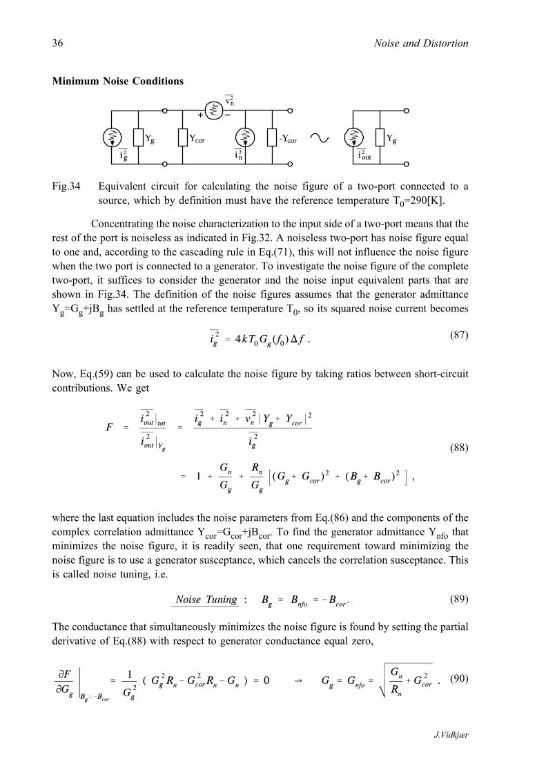
Concentrating the noise characterization to the input side of a two-port means that the
Fig.34 Equivalent circuit for calculating the noise figure of a two-port connected to asource, which by definition must have the reference temperature T0=290[K].
rest of the port is noiseless as indicated in Fig.32. A noiseless two-port has noise figure equalto one and, according to the cascading rule in Eq.(71), this will not influence the noise figurewhen the two port is connected to a generator. To investigate the noise figure of the completetwo-port, it suffices to consider the generator and the noise input equivalent parts that areshown in Fig.34. The definition of the noise figures assumes that the generator admittanceYg=Gg+jBg has settled at the reference temperature T0, so its squared noise current becomes
Now, Eq.(59) can be used to calculate the noise figure by taking ratios between short-circuit
(87)
contributions. We get
where the last equation includes the noise parameters from Eq.(86) and the components of the
(88)
complex correlation admittance Ycor=Gcor+jBcor. To find the generator admittance Ynfo thatminimizes the noise figure, it is readily seen, that one requirement toward minimizing thenoise figure is to use a generator susceptance, which cancels the correlation susceptance. Thisis called noise tuning, i.e.
The conductance that simultaneously minimizes the noise figure is found by setting the partial
(89)
derivative of Eq.(88) with respect to generator conductance equal zero,
(90)
J.Vidkjær

37IV-3 Noise Characterization of Two-Ports
The 2nd order derivative becomes 2RnGnfo2/Gg
3, which is positive if Gg is positive, so theresult above gives a minimum in noise figure. Simultaneous use of the two conditions iscalled noise matching, where
The corresponding minimum noise figure is found by inserting Ynfo into Eq.(88),
(91)
Substituting this result back into Eq.(88), the noise figure with an arbitrary generator admit-
(92)
tance is written
Note, in this form four parameters are still needed to characterize the noise properties of the
(93)
two-port, namely Fmin, Rn, and the two components Gnfo, Bnfo of the generator admittanceYnfo that minimizes the noise figure.
Constant Noise Figure Circles
Commonly the optimum generator admittance with respect to noise for a transistordiffers from the choice that would be optimal regarding gain and stability considerations alone.The designer must compromise between the two concerns. An aid to decisions is to mapcontours of constant noise figures. They constitute a system of circles with centers in ygcn andradii gcn , where
(94)
J.Vidkjær

38 Noise and Distortion
These expressions are verified by observing that a circle of center ygcn and radius gcn in thecomplex Yg-plane is described by
Expanding the noise figure in Eq.(93) with the circle expression in mind, using Gg=
(95)
½(Yg+Yg* ), gives temporarily
By this step the center ygcn in Eq.(94) is identified from the coefficients to either Yg or Yg*.
(96)
To complete the circle requirement and get the radius, we add ygcnygcn* to both sides of the
last equation, i.e.
(97)
The set of parameters containing the minimum noise figure Fmin, the series noiseequivalent resistance Rn, and the optimal generator admittance Ynfo, or the equivalent setsbased on the generator reflection coefficient, are becoming more and more common in devicedata sheets. The relationship between the two forms is straightforward to establish, albeit itneeds a little algebra. Reflection coefficients for impedances and admittances were introducedin Chap.II sec.8. With reference impedance Z0, which is real, the generator and optimumadmittances are expressed by their reflection coefficients through
(98)
(99)
J.Vidkjær

39IV-3 Noise Characterization of Two-Ports
Inserting into the last expression from Eq.(93) yields
Moving from admittance plane to reflection plane is represented by the Smith chart. The
(100)
underlying transformation maps circles into circles, so contours of constant noise figures inan admittance plane become also a system of circles in a reflection plane or a Smith chart. Toget the corresponding centers and radii we rewrite Eq.(100) to read
Like the previous computation in Eq.(96), it is the Γg and Γg* coefficients that determine the
(101)
(102)
center of the circle. The radius is adjusted accordingly afterwards. Above in Eq.(102) this isanticipated by adding and subtracting the upcoming center term in absolutely squared format the right hand side. Rearranging this equation gives the constant noise figure circles,
Here centers and radii are denoted Γgcn and ρcn respectively. The noise figures for the circles
(103)
are expressed through the quantity N that was defined in Eq.(101).
Example IV-3-3 ( noise figure circles in Y-plane )
Fig.35 shows constant noise figure circles for two collector bias currents in agenerator admittance plane for a bipolar transistor, BFR91A. All centers of the circle systemin each figure have equal imaginary parts, which is in agreement with the first equation in(94), where the second non-constant term is real.
J.Vidkjær

40 Noise and Distortion
In design considerations it is sometimes convenient to use the primary equivalent two-
Fig.35 Extract from Philips Data Handbook, SC14 RF Wideband Transistors, VideoTransistors and Modules, 1993.
port input noise parameters Rn, Gn, and Ycor=Gcor+jBcor from Fig.33(b). Calculating back-wards from Fmin and Ynfo=Gnfo+jBnfo, keeping Rn and using Eqs.(92),(91), provides
(104)
J.Vidkjær

41IV-3 Noise Characterization of Two-Ports
Table II Extraction of noise equivalent circuit parameters for BFR91Afrom data in Fig.35
IC, VCE 4 mA, 8 V 30 mA, 8 V
Fmin 1.6 dB ∼ 1.45 2.3 dB ∼ 1.70
Gnfo 8.0 mS 13.5 mS
Bnfo 1.7 mS -0.75 mS
gcn 29.4 mS 28.1 mS
F @ gcn 3.5 dB ∼ 2.24 4.0 dB ∼ 2.51
Rn 17.4 Ω 22.6 Ω
Gcor 4.96 mS 1.97 mS
Bcor -1.7 mS 0.75 mS
Gn 0.68 mS 4.04 mS
gm/2β=IC/0.026/180 0.85 mS 6.41 mS
Gn,tot=Gn+|Ycor|2Rn 1.16 mS 4.14 mS
While Fmin and Ycor are directly recognized in the above figures, Rn must be calculated froma circle radius gcn and the corresponding noise figure. By Eq.(94) we get
Table II summarizes data that are deduced from the two systems of circles in Fig.35 by the
(105)
expressions above. The first five rows contain direct readings and the next four hold parame-ters of the input equivalent circuit. The two bottom rows are included to illuminate the resultswhere first the gm/2β value is the idealized value of Gn. To see this we recall fromEqs.(83),(84) that Gn controls an uncorrelated source, which according to the discussions onpage 17 is the shot noise associated with the base current in the transistor. Using IB=IC/β weget from Eq.(36)
Table entries correspond to a typical β=90 value from the data sheets and Vt=26mV. They are
(106)
relatively close to the extracted Gn´s. It is supposed that the observed overestimation in the
J.Vidkjær

42 Noise and Distortion
check values are caused by reductions of the actual transistor conductances due to highinjections. The last row indicate the significance of correlation by showing the value of Gnthat correspond to the total input noise shunt current. Especially in the low current case thedifference and thereby the correlation is pronounced. This is in agreement with the fact thatthe transistor input impedance is relatively high at low currents where the input noise voltagesource encompasses the effect of the collector noise current if the generator impedance is low.Example IV-3-3 end
Example IV-3-4 ( noise figure circles in Smith chart )
Fig.36 shows noise circles in Smith chart representing generator impedances. Thereare two system of circles. The closed ones at the right hand side are the noise figure circlescorresponding to Eq.(103). The four corresponding noise parameters are also given. The othersystem includes circular arcs,7 where the input impedance provide constant gain if thetransistor is matched conjugatedly at the output port, i.e. curves of constant available powergain. Transforming to admittance or impedance form, the noise parameters are
At the particular bias and frequency, the transistor is potentially unstable and cannot
(107)
be simultaneously matched at both ports with respect to power. This is the reason why theSmith chart is divided by a so-called stability circle. Generator impedances map into outputimpedances of negative real parts in the unstable region. The arc of highest gain, which isshown in the figure, is 11.2dB. It is called MSG and equals is the maximum stable gainGms=|y21/y12|=|s21/s12| that was introduced in chap.III, p.13.
The Smith chart in the example shows that it is possible to construct a stableamplifier of gain equal to Gms with a noise figure slightly below 3dB. Sacrificing gain, theoptimum noise figure of 2dB may be achieved with an available power gain of approximately8dB. To see the further consequences of such a choice we need small-signal parameters forthe transistor. In the present case they are transformed from data sheet s-parameters to read
(108)
7 ) It is proven in most literature on RF amplifiers, for instance [8] or chap.III ref’s [5],[6], that curves of constant power gain constitute a systems of circles in either Smithcharts or impedance and admittance planes.
J.Vidkjær

43IV-3 Noise Characterization of Two-Ports
Highest gain with minimum noise figure is achieved when the load yL equals the
Fig.36 Extract from Philips Data Handbook, SC14 RF Wideband Transistors, Video Tran-sistors and Modules, 1993.
complex conjugated of the transistor output admittance using the optimal noise figuregenerator admittance Ynfo at the input port. We get
(109)
J.Vidkjær

44 Noise and Distortion
The corresponding available gain and the stability factor in augmented estimation are
(110)
The gain becomes a little more than 8 dB in agreement with Fig.36, where the point of
(111)
optimum noise figure is slightly above this gain arch. The K-factor is far below the ideal offive that makes a parameter insensitive amplifier, so one of the penalties of getting minimumnoise figure with most gain from this transistor is that the resultant amplifier may be difficultto tune. Another drawback is that the input port becomes highly mismatched. The inputadmittance and impedance of the amplifier are
which implies a mismatching of
(112)
(113)
According to the previous discussion in chap.III,p.15 ff., the mismatch pertains ateither side of any lossless input matching network. Therefore, it will also be present at theinput port to any amplifier designed to minimum noise figure with most gain around thistransistor. The mismatch is rather high and may be impractical. To lower it we may eitherreduce gain, sacrifice noise figure, or both. As an example, applying an ohmic load of 50Ωin parallel with a capacitor of 15.9pF (yL=20mS+j10mS) provides gain - transducer gain asthe output port is no longer matched - and stability factor that are calculated using
(114)
J.Vidkjær

45IV-3 Noise Characterization of Two-Ports
The corresponding input admittance and mismatching properties are
(115)
In this case we maintain the minimum noise figure and obtain an amplifier that has improved
(116)
(117)
the input mismatch at the expense of gain. Another choice with the same ohmic load couldbe to optimize gain letting an input matching network provide conjugated matching to theinput admittance from Eq.(116). In that case the input power equals the available power, soit is relevant to consider the operational power gain, which yields
To find the corresponding noise figure, Eq.(93) is employed with generator admittance equal
(118)
to the complex conjugated input admittance, i.e.
Clearly, the noise figure increases when the generator admittance differs from the optimal one,
(119)
instead we achieve higher gain, better stability and no mismatch at the input port.Example IV-3-4 end
J.Vidkjær

46 Noise and Distortion
J.Vidkjær

47
IV-4 Distortion in Almost Linear Circuits
The type of distortion we consider in this section is the so-called nonlinear distortion,i.e. departures from linear input-output relationships of electronic circuits and components.Nonlinear distortion accompanies large drive signals and sets an upper bound on the operationlevel for proper performance of many intentionally linear circuits.
Fig.37 Nonlinear two-port example, a voltagecontrolled voltage generator circuit.
(120)
To fix ideas of a circuit that eventually exhibits nonlinear distortion, the voltagecontrolled voltage source in Fig.37 is considered. It could be a DC-coupled voltage amplifierwith a simple, memoryless input-output relationship like Eq.(120). Taken as a function of theentire input range in Vi, this general form is a large-signal expression, which is commonly notlinear. Linear amplification is established in restricted input intervals around the DC biasingpoint and expressed mathematically by the first order term of a Taylor expansion in thedeviation vi from the bias Vi0,
Subdividing output into bias and a small-signal part yields
(121)
where the a, b, c, and possibly more coefficients of the small-signal polynomial are shorthand
(122)
notation for the scaled derivatives of the original, large-signal expression,
In an amplifier the a coefficient would be the small signal voltage gain and the higher order
(123)
terms b and c introduce distortion. To keep distortion low we should select components withsmall second, third and even higher order expansion terms or hold the signal level low, sopowers in vi stay insignificant. The nonlinear expansion coefficients b, c, etc. refer to DC and
J.Vidkjær

48 Noise and Distortion
instant voltages or currents. If DC bias is unimportant, a polynomial expansion may expressdistortion directly in RMS scale, i.e.
One of the most prominent consequences of the nonlinear distortion is the occurrence
(124)
of deterministic signal components at frequencies that are not present in the input signal. Nostrictly linear circuits are able to do that and there are several technical utilizations of theproperty, mixing for instance. In this section we shall, however, concentrate on the differentways in which nonlinear effects may degrade the performance of RF communication circuitsand on methods of quantifying this in data sheets.
A precautionary word on the validity of our results is in place. To let the responseof a nonlinear circuit be represented by a Taylor series expansion requires that all nonlineari-ties combine memoryless. This will be the case with algebraic characteristics in ohmicnetworks, but typically not if the problem includes combinations of linear and nonlinearconductances and reactances. In such cases more powerful but also significantly more labori-ous methods are required to conduct genuine analytical treatments. Volterra series expansions -introduced in ref´s [21] or [22] chap.4 - are suggestions for that purpose. Using thesemethods we get expansion coefficients corresponding to the a, b, and c’s above, which becomefrequency dependent. However, no more frequency components arise with combinednonlinearities compared to the ones that are demonstrated by Taylor series expansions, whichtherefore suffice for the present purpose of exploring basic matters. They also suffice in designif the polynomial coefficients are deduced from data that apply to the actual operatingfrequencies.
Simplifying concerns are also the reason why expansions mostly are limited toencompass third order terms only. Going higher would provide no really new phenomena buta lot more messy algebra.
Single Signal Distortions
Fig.38 shows the single sided frequency components in the amplifier voltages whena single tone input signal drives the circuit that was described by Eq.(122),
The frequency components in the output emerge when the trigonometric identities,
(125)
(126)
J.Vidkjær

49IV-4 Distortion in Almost Linear Circuits
are applied to the polynomial input-output relationship. The different terms become
Fig.38 Signal and distortion components when a single tone input signal is applied to acircuit which includes nonlinear components.
(127)
The first order term is the conventional linear small-signal gain term. The second order termin the Taylor expansion causes a DC contribution and a second harmonic component. Caremust be taken, both in circuit analysis and in practical design, to ensure that proper biasingof the component persists even when the quadratic term adds to the DC voltage or current.The third order term produces both a component at the input frequency and a third harmoniccomponent. It is possible in many application to discard the effects of higher harmoniccomponents by filtering. But it is impossible to remove the distortion component from thesignal at the fundamental frequency, so the third order term will always cause distortion.Therefore, third order terms often draw most attention in specifications and data sheets.Actually all odd ordered Taylor expansion terms would contribute to the fundamental signalcomponent, but their significance decrease rapidly with raising order in electronic devices thatare intended for linear operation and driven accordingly, so we stay with the third order maxi-mum below.
Including all frequency components, except DC, gives a measure called the totalharmonic distortion, KTHD, in an amplifier. It includes all components, i.e.
J.Vidkjær

50 Noise and Distortion
The approximations in the distinct second, third, or possible higher harmonic terms like K2
(128)
(129)
and K3 require that the third order term at the signal frequency is small compared to the firstorder term, i.e. ¾c/a A2 1. The assumption is necessary for calculating the total distortionfrom experimental data, because it is difficult to distinguish between fundamental frequencyoutputs arising from the first and the third order terms in measurements.
Removing all but the signal frequency components from the output, as indicated by
Fig.39 Amplifier or other electronic component followed by a bandpass filter that removesall but signal components around the fundamental frequency.
the setup of Fig.39, leaves the first third order term in Eq.(127)(c) as the only disturbingcomponent in observation. Fig.40 shows a typical shape of the input to filtered output charac-teristics of amplifiers or transistors, where the output signal falls below the linear extrapolationat higher signal levels. This is called compression and may be characterized by the RMS inputdrive level, Vi,1dB, where the compression corresponds to 1dB output signal reduction or,equivalently, an output amplitude reduction by at factor of 0.891 compared to the assumedlinear value. In terms of the Taylor series expansion, the compression level becomes
Absolute values of the Taylor coefficients are required above to account for the fact that a and
(130)
c must be of opposite signs if the resultant output amplitude falls below the linear term. Theresult is scaled to RMS values, that are common in data sheets and instrument readings.
J.Vidkjær

51IV-4 Distortion in Almost Linear Circuits
Instead of referring to the input side, compression specifications refer typically to the
Fig.40 Amplifier characteristics with compression. Coefficients a and crms must be ofopposite signs. Input and output hold fundamental frequency components only.
Fig.41 Amplifier characteristics in dB scale. Gains are represented by lines of slope equalto one with values given by the vertical positions.
output side by giving an output power level and a gain, either the stipulated linear Glin or theactual gain at 1dB compression, G1dB. Backtracking from powers to voltages requires thatinput and output impedances are defined. Dealing with amplifier blocks this is commonly nota problem whereas transistor data often require careful review before interpretation. For thesetup in Fig.39 the powers and the power gains are
Absolute power indications may by in dBm, decibels relative to 1mW. Translated to dB scales,
(131)
the linear region of the input-output plot in Fig.41 shows
(132)
J.Vidkjær

52 Noise and Distortion
Inserting the voltage for 1dB compression from Eq.(130), the corresponding input and outputpowers are expressed,
(133)
Distortions with Two Signals
Applying two sinusoids of sufficient amplitudes to an amplifier that eventuallybecomes nonlinear may produce a multitude of frequency components in the output spectrum.With two tones input to the Taylor expansion,
we get all the components that are shown below in Fig.42 and Eq.(136). They are calculated
(134)
from the trigonometric identities in Eq.(126) with supplement of the product formula,
For illustrating purposes the two input signal components in Fig.42 are chosen with
(135)
Fig.42 Output signal and distortion components with two-tone signal input to a nonlinearcomponent.
close frequency spacing, which is an important situation in practice. In that case we still referto the fundamental input frequency in the meaning of the range around ωa and ωb. Regardingoutput components in Eq.(136), the first observation is that all terms generated from a singletone in Eq.(127) are present with unaltered powers of amplitudes for both the ωa and the ωbinput components. It is also observed that the second order Taylor term causes componentsaround DC and around twice the fundamental input frequency. This is equivalent to the singletone case. There is also resemblance in the third order term, which produces a complex ofcomponents in the fundamental frequency range and a complex around third harmonics.
J.Vidkjær

53IV-4 Distortion in Almost Linear Circuits
News with two tones are the different possibilities for interaction between the two.
(136)
The second order terms in Eq.(136)(b2) and the third order terms in (c3) and (c4) contain so-called intermodulation products, where especially the last ones may cause troubles if theresultant frequencies hit the desired fundamental frequency range. Moreover, there is a directcross-coupling between the two signals at their fundamental frequencies through the thirdorder distortions terms in Eq.(136)(c1). The latter have great practical importance in radioreceiver design causing blocking and cross-modulation effects, which we shall consider below.Keep in mind here that the cosine functions are indifferent with respect to sign of thearguments, so in comparisons the terms follow signs of the coefficients a, b, and c.
Blocking is a condition that occurs when two signals are present at the input to anamplifier which has a narrow channel selecting bandpass filter in the output port. As sketchedin Fig.43(a), the input holds a week signal, which is the one we are supposed to receive, soits frequency ωa lies in the passband. The other signal is much stronger. Albeit close infrequency to the desired signal, its frequency ωb falls outside the passband of the filter. Thetotal output from the passband gets the amplitude,
J.Vidkjær

54 Noise and Distortion
It is assumed that the A signal is so small, that its own third order distortion term may be
Fig.43 Input and output components illustrating signal desensitization towards blocking.
(137)
ignored. When it is also supposed that the nonlinearity is of compression type, so the a andc coefficients have opposite signs, the last expression clearly shows that the undisirable Bsignal controls the size of the received signal. Blocking is the condition where the receivedsignal disappears, i.e. V̂o = 0 in Eq.(137). The corresponding RMS value of the B signal is
The situation where the received signal still is present, but significantly reduced by the
(138)
neighboring signal - like Fig.43(b) - is sometime called desensitization.
Fig.44 Input and output components illustrating cross-modulation. The selected ωa signalis inflicted by the modulation of a neighboring but undesired channel around ωb.
Cross modulation is the situation where the modulation in a large out-of-band signaltransfers to a smaller signal in reception. For clarity the latter signal is represented by theunmodulated carrier at frequency ωa. We suppose that the B signal is amplitude modulatedby a low frequency sinusoid at ωm with modulation index m, which is smaller than one,
(139)
J.Vidkjær

55IV-4 Distortion in Almost Linear Circuits
The squared value of disturbing signal is approximated,
where it is assumed again that the signal to be received is small enough to let its own distor-
(140)
tion be ignored on insertion into Eq.(136)(c1). The resultant passband output gets thereby aform that clearly shows transfer of modulation from the B signal to the A signal with aresultant modulation index m̂,
A common way of specifying cross modulation is to give the RMS voltage of the disturbing
(141)
out-of-band carrier, which corresponds to 1% overcoupled modulation, i.e.
(142)
(143)
Fig.45 Input and output components illustrating hum-modulation. The low-frequency ωbsignal translates to an amplitude modulation of the RF signal at ωa.
Neighboring input signals interacts through the third order terms since they canproduce frequency components close or equal to the original ones. Interaction between widelyseparated frequency components may occur by other terms. An example is interaction betweena RF signal of frequency ωa and a LF signal at ωb, which is illustrated in Fig.45. Examplesare low-frequency components from insufficient smoothing and decoupling of the bias insensitive amplifiers. The second order terms in Eq.(136)(b2) may be rejoined to give,
(144)
J.Vidkjær

56 Noise and Distortion
The last expression demonstrates that the LF signal amplitude modulates the RF signal withan AM modulation index given by
This phenomenon is sometimes called hum-modulation because it could be heard in many
(145)
older receivers where it stemmed from the AC supply.
Common in all the examples above is that a signal in the passband and a signaloutside enter a device that is nonlinear at large drive levels. The interaction leaves distortioncomponents that cannot be removed by subsequent filtering. To anticipate the thought that wecould apply filtering at the input side and avoid all the troubles, it should be recalled that intunable receivers, bandpass filtering is done in the IF section after the RF signal is transferredto the intermediate frequency by a mixer, cf. Chap.I, Sec.5. In such receivers, the passbandindications above must be interpreted as the effect of IF filtering transferred in frequency tothe RF band. It should also be mentioned at this point that mixers introduce distortion defectslike compression and cross-modulation. They are characterized and quantified by the sameconcepts we are introducing here for components and amplifiers, the only exception being thatinput and output fundamental frequencies do not coincide but differ by the frequency of thelocal oscillator. We shall return to the matters below when mixers are considered explicitly.
Intercept Points
Distortion specifications may be directly related to the practical consequences ofintermodulation, for instance by cross-modulation as exemplified by Eq.(143). Recall,however, that all the implications of distortion we have considered express basically theabsolute ratio of a higher order expansion term over the fundamental frequency term. A simpleand easily interpretable way to get this information experimentally is by so-called interceptpoints. Below we start concentrating on the most important third order distortion and theassociated 3rd order interception point. Afterwards the less frequent second order points,which develop equivalently, cf.[23] chap.10, is summarized briefly.
Fig.46 Third order intercept point conditions, (a) equal inputs, sufficiently low to ignore(b) compression terms in outputs. Experimental data are often dBm scaled like (c).
J.Vidkjær

57IV-4 Distortion in Almost Linear Circuits
Intercept points are recorded from two-tone setups where the two input amplitudesare equal. Using Eq.(136), B is set equal to A while the frequencies ωa and ωb still differ. Apicture of this situation preparing third order intercept point determination is shown in Fig.46.The two output components corresponding to the two-tone input are equal if ωa is sufficientlyclose to ωb. We call the corresponding output amplitude Vo1. The two intermodulationproducts at nearby frequencies 2ωa-ωb and 2ωb-ωa are also practically equal in size each ofamplitude Vo3. With common input amplitudes, Vi1=A=B, one linear gain term fromEq.(136)(a) and one intermodulation term from Eq.(136)(c4) are
Corresponding powers of input and output components with input and load resistances Rin and
(146)
RL respectively
Considered as function of input power Pin, the intermodulation term Po3 rises much faster than
(147)
the linear term Po1. Their ratio, often called the intermodulation ratio or - in dB scale - theintermodulation distortion, IMD, is
The third order intercept point is the stipulated crossing point between Po1 and Po3 where the
(148)
intermodulation ratio is one, and input and output powers Pi,IP3, Po,IP3 are
Translating the above results to dB scales provide a simple and easily interpretable
(149)
graphical presentation as seen in Fig.47 where,
When assumptions of no compressions are met, the fundamental frequency term Po1[dBm]
(150)
grows in direct proportion to Pi[dBm] - slope equal to one - while the third order inter-modulation term Po3[dBm] grows linearly, but faster with a slope of three. Above certain drivelevels, the assumptions are no longer met and experimental data start falling below theassumptions. Po1 is lowered by compression as described formerly on page 50 while lowering
J.Vidkjær

58 Noise and Distortion
of Po3 is caused by odd-numbered higher order terms which we commonly disregard under
Fig.47 Third order intercept point: Crossing of a fundamental frequency output Po1 and a3rd order intermodulation product, Po3, both in straight line stipulations.
small signal excitations. Dealing with experimental data that bend as sketched in the figure,it is still easy to draw linear extrapolations and find the intercept point. In dB scale we get
Comparing the last result with the 1dB compression output power, Po,1dB from Eq.(133), we
(151)
must expect that under similar conditions, i.e. same frequency, same bias i.e. same a and ccoefficients, and same load impedances, the output power at the intercept points should lie10.6 dB above the 1dB compression level, if a simple Taylor expansion is quantitatively ade-quate for the circuit in consideration8.
The second order intercept point concerns the intermodulation product of frequencyequal to either the sum or the difference of the two input signals, i.e. the first or the secondterm in Eq.(136)(b2). In analogy with Eqs.(146) to (148), keeping in mind that the inputpower expressions for Pi and P01 stay unaltered from the third order case, we get,
(152)
(153)
8 ) A common violation of the assumption occurs when the output swing is limited bypower supply, so the amplifier or device is driven into heavy saturation and/or cut-off. Taylor expansions with three terms are not adequate for characterizing suchabrupt events that might include relaxation effects.
J.Vidkjær
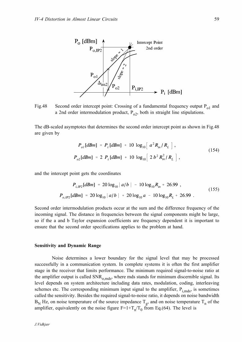
59IV-4 Distortion in Almost Linear Circuits
The dB-scaled asymptotes that determines the second order intercept point as shown in Fig.48
Fig.48 Second order intercept point: Crossing of a fundamental frequency output Po1 anda 2nd order intermodulation product, Po2, both in straight line stipulations.
are given by
and the intercept point gets the coordinates
(154)
Second order intermodulation products occur at the sum and the difference frequency of the
(155)
incoming signal. The distance in frequencies between the signal components might be large,so if the a and b Taylor expansion coefficients are frequency dependent it is important toensure that the second order specifications applies to the problem at hand.
Sensitivity and Dynamic Range
Noise determines a lower boundary for the signal level that may be processedsuccessfully in a communication system. In complete systems it is often the first amplifierstage in the receiver that limits performance. The minimum required signal-to-noise ratio atthe amplifier output is called SNRo,mds, where mds stands for minimum discernible signal. Itslevel depends on system architecture including data rates, modulation, coding, interleavingschemes etc. The corresponding minimum input signal to the amplifier, Pi,mds, is sometimescalled the sensitivity. Besides the required signal-to-noise ratio, it depends on noise bandwidthBN Hz, on noise temperature of the source impedance Tg, and on noise temperature Tn of theamplifier, equivalently on the noise figure F=1+Tn/T0 from Eq.(64). The level is
J.Vidkjær

60 Noise and Distortion
where the temporarily included Gav is the available power gain of the amplifier. If there is no
(156)
association to specific system requirements, the acceptable output signal level from anamplifier may be taken equal to its noise output, i.e. using SNRo,mds=1. If, furthermore, thesource impedance is supposed to be at the reference temperature, Tg=T0=290 K, the minimumdiscernible level gets a simpler form that sometimes is seen in literature,
The dynamic range of an amplifier indicates the span of useful input levels. It is
(157)
commonly the distance - in decibels - from the minimum discernible signal to the upperbound. Several upper bound criteria are possible, a simple one being the so-called spuriousfree dynamic range. The upper bound is the input level where the third order intermodulationterm Po3 passes the noise floor at the amplifier output. The noise floor is taken as the outputcorresponding to the minimum discernible signal from Eq.(156). Triangle considerations inFig.49 provide a simple expression for the spurious-free dynamic range,
where third order intermodulation is parameterized through the third order intercept point input
(158)
level Pi,IP3.
Fig.49 Spurious-free dynamic range, Dspf dB, the distance in input power levels where thethird order intermodulation and the signal exceed the noise floor respectively.
J.Vidkjær

61IV-4 Distortion in Almost Linear Circuits
Alternative dynamic range specifications use upper bound input that gives a minimum
Fig.50 Dynamic range specifications with upper bound set by (a) intermodulation productor (b) compression.
intermodulation ratio, for instance 40dB, or a certain amount of gain compression, for instance.1 or 1 dB. These two cases are summarized by Fig.50. To express the intermodulationbounded dynamic range, DimX, Eqs.(148),(149) are combined to give the input power for arequired intermodulation ratio Δim3X in terms of the third order intercept point,
Now the intermodulation bounded dynamic range is expressed
(159)
Compression is commonly specified by a single tone test and expressed separately. When the
(160)
compression levels of specification equals the upper dynamic range bound, the correspondingdynamic is given by
The last expression uses data that refer to the output side, i.e. the output power level at XdB
(161)
compression and the linear gain Glin prior to compression.
J.Vidkjær

62 Noise and Distortion
Problems
P.IV-1
Assume narrowband conditions and show that the noise-bandwidth of the transmis-
Fig.51
sion from signal source EG to v2 in Fig.51 becomes π/2 times the 3dB bandwidth likethe RC circuit in Example IV-1-1. What is the RMS noise voltage at port 2 ifRG=50Ω @ 290[K] and the circuit has center frequency f0=100 MHz with 3dBbandwidth BW3dB=10 MHz?
P.IV-2An amplifier, which has ohmic optimal noise admittance, ynfo=gnfo, and ignorableinput and correlation admittances, yin, ycor→0, is driven from a source with ohmicgenerator admittance at 290[K] where yG=gG<gnfo. Show and explain the fact thatif the input port of the amplifier is shunted by a resistor to provide noise matching,the resultant output SNR decreases compared to the case with no shunting resistance.
P.IV-3 9
A QPSK signal is transmitted at 45 Mbps rate and is received as shown in Fig.52.
Fig.52
The attenuation from the transmitter to the receiver is 120dB and the antenna has thenoise temperature Ta=55°K. The noise figure of the RF amplifier corresponding tothe antenna impedance is F=3.5 dB.Calculate the transmitter power Pt[W] corresponding to the resultant bit error ratesof 10-5, 10-6, and 10-7 respectively.
P.IV-4 9,10
A satellite transmits from a distance of 36000 kM a 1.2 Mbps QPSK modulatedsignal on a 12.2 GHz carrier. The transmitter power is 100 W and the satellite
9 ) Review chap.I pp 24-27 on bit error rates in digital modulations.
10 ) Review Friis’ transmission formula and antenna areas
J.Vidkjær

63IV Problems
antenna gain is 27 dB. At the receiver site, the antenna has the noise temperature52°K and the noise figure of the input amplifier is 2.5 dB at the antenna impedanceof 50Ω.Find the receiver antenna gain and the antenna area that are required to get BER <10-4. What is the corresponding signal voltage at the receiver amplifier input ?
P.IV-5 9
Fig.53
The transmission system in Fig.53 operates in QPSK modulation at rate Rb = 102Mbps. The carrier frequency is f0=14.2 GHz and the 122 dB attenuation is from thetransmitter output power to the RF amplifier input. It is supposed that all componentsare matched at impedance level Zo=50Ω.What is the RF amplifier input signal to noise ratio per bit Eb /η if a bit error rateof BER = 10-6 is required ? Find the corresponding transmitter output power.
What are the 1dB compression input and output levels for the transmitter poweramplifier if it is supposed that 0.2 dB compression or less has no significant influenceon the resultant bit error rate ?
Repeat the above calculations when a low-noise front amplifier is inserted as shownby Fig.54.
P.IV-6
Fig.54
The transistor in Example IV-3-3, biased by IC=30mA and VCE=8V, has at 800 MHzthe following y-parameters
(162)
J.Vidkjær

64 Noise and Distortion
The transistor is driven by a 50Ω impedance and loaded by 25Ω as shown in Fig.6.
Fig.55
The input and output resonance circuits are designed independently neglecting feed-back to approximate synchronous tuning around 800 MHz with 3dB bandwidth equalto 80 MHz. It is assumed that the generator and load impedances are at the referencetemperature of 290K. Data sheets specify 1dB compression at 36 dBm output powerif the transistor is loaded with 75Ω. It is supposed that this level reduces to 28 dBmwhen the load is 25Ω.- Verify that it is legal to disregard feed-back effects when the tuning conditions arecalculated. Find the operational, the transducer and the available power gainsfor the amplifiers and explain their differences.
- What is the noise figure of the amplifier ?- Find the noise bandwidth of the amplifier if it assumed that it corresponds to thesynchronously tuned characteristic. What is the total RMS output noise voltage atthe amplifier output port ?
- Calculate the amplifier sensitivity in terms of input available power and find thecorresponding 50dB 3rd order intermodulation bounded dynamic range.
P.IV-7
Fig.56 shows a single-tuned differential amplifier that is tuned to center frequency
Fig.56
fo. The differential current is expressed
J.Vidkjær

65IV Problems
The bias current is I=5mA. The input signal is amplitude modulated,
(163)
The modulation index is m=1, and it is assumed that the modulating frequency is so
(164)
low, that the sideband transistor load impedance is the same as the center frequencyimpedance. The nonlinear characteristic in Eq.(163) causes distortion in the low-frequency envelope at the output from the amplifier. Derive an expression for thethird harmonic contribution K3 to the total harmonic distortion of the output enve-lope, the so-called third order modulation distortion. Find the values with Vs = 1mVand 10mV. Assume that the voltage bias and RL are chosen to prevent transistorsaturation.
J.Vidkjær

66 Noise and Distortion
References and Further Reading
[1] M.S.Gupta,ed., Electrical Noise: Fundamentals & Sources, IEEE press, 1977Includes 22 papers on basic noise properties and extensive bibliographies.
[2] M.S.Gupta,ed., Selected Papers on Noise in Circuits and Systems, IEEE press,1988. Includes 13 more papers on noise.
[3] H.F.Cooke,"Microwave Transistors: Theory and Design", Proc.IEEE, vol.59,pp.1163-1181,Aug.1971, reprinted in [8].
[4] A.van der Ziel, Noise in Solid State Devices and Circuits, Wiley, NY 1987.
[5] M.S.Keshner,"1/f Noise",Proc.IEEE, Vol.70, No.3, pp.212-218, March 1982.
[6] ITT Reference Data for Radio Engineers, Sams, NY, 1968
[7] W.C.E.Lee, Mobile Communications Engineering, McGraw-Hill NY, 1982
[8] H.Fukui,ed., Low-Noise Microwave Transistors and Amplifiers, IEEE press, 1981.Includes 60 papers on device noise and low-noise design.
[9] H.C.de Graff, F.M.Klaassen, Compact Transistor Modelling for Circuit Design,Springer, Wien-N.Y, 1990.
[10] Y.P.Tsividis, Operation and Modeling of the MOS Transistor, McGraw-Hill, N.Y.1988.
[11] A.van der Ziel, "Noise in Solid-State Devices and Lasers", Proc.IEEE, vol.58,-pp.1178-1206, Aug.1970. Reprinted in [1].
[12] C.D.Bulucea, D.C.Prisecaru,,"The Calculation of the Avalanche Multiplication Factorin Silicon P-N Junctions Taking into Account the Carrier Generation ( Thermal orOptical ) in the Space Charge Layer",IEEE trans.,Vol.ED-20,pp.693-701,Aug.1973.
[13] P.Antognetti, G.Massobrio, eds., Semiconductor Device Modeling with SPICE,McGraw Hill,1988.
[14] H.Statz,H.A.Hauss,R.A.Pucel,"Noise Characterization of Gallium Arsenide Field-Effect Transistors",IEEE trans. Electron Devices, vol. ED-21,pp.549-562, Sept.1974.,reprinted in [8].
[15] H.A.Haus, R.B.Adler, Circuit Theory of Linear Noisy Networks, Technology Press,Wiley, 1959.
[16] J.Engberg, S.T.Larsen, Noise Theory of Linear and Nonlinear Circuits, Wiley 1996.
[17] IRE Standards on Methods of Measuring Noise in Linear Twoports, 1959, Proc.IRE,vol.48, pp.60-68, Jan.1960, included in [8].
J.Vidkjær

67IV References and Further Readings
[18] A.van der Ziel, Noise: Sources, Characterization, Measurement, Prentice-Hall N.Y.1970.
[19] H.T.Friis,"Noise Figures of Radio Receivers", Proc.IRE vol.32, pp.419-422, July1944. Reprinted in [8].
[20] H.Rothe, W.Dahlke, "Theory of Noisy Fourpoles" Proc.IRE, vol.44, pp.811-818, June1956, reprinted in [8].
[21] Y.L.Kuo,"Frequency-Domain Analysis of Weakly Nonlinear Networks, "Canned"Volterra Analysis", IEEE Circuit and Systems Magazine, aug.1977, pp.2-8 (part 1),and Oct.1977, pp.2-6 (part 2).
[22] S.A.Maas, Nonlinear Microwave Circuits, Artech, Boston 1988.
[23] R.S.Carson, Radio Communications Concepts: Analog, Wiley NY. 1990.
J.Vidkjær

68 Noise and Distortion
J.Vidkjær

69
Index
1/f Noisesee Flicker Noise . . . . . . . . . . . 8
Avalanche noise . . . . . . . . . . . . . . . 11Bipolar Junction Transistor, BJT
see Bipolar Transistor . . . . . . . . 17Bipolar Transistor
noise . . . . . . . . . . . . . . . . . . . 17Blocking . . . . . . . . . . . . . . . . . . . . . 53Boltzman´s Constant . . . . . . . . . . . . 2Burst noise . . . . . . . . . . . . . . . . . . . 11Carson
noise theorem . . . . . . . . . . . . . 6Compression . . . . . . . . . . . . . . . . . . 50Correlation Coefficient . . . . . . . . . . . 33
FET gate and drain noise . . . . . 24Cross Modulation . . . . . . . . . . . . . . 54Desensitization . . . . . . . . . . . . . . . . 54Diode
noise . . . . . . . . . . . . . . . . . . . 15Distortion
almost linear circuits . . . . . . . . 47compression . . . . . . . . . . . . . . 50cross modulation . . . . . . . . . . . 54hum . . . . . . . . . . . . . . . . . . . . 55modulation . . . . . . . . . . . . . . . 65single tone . . . . . . . . . . . . . . . 48total harmonic, THD . . . . . . . . 49two-tone . . . . . . . . . . . . . . . . . 52
Dynamic Range . . . . . . . . . . . . . . . . 60compression bounded . . . . . . . . 60intermodulation bounded . . . . . . 60spurious free . . . . . . . . . . . . . . 60
Electron Charge . . . . . . . . . . . . . . . . 6Field Effect Transistor
noise . . . . . . . . . . . . . . . . . . . 22Flicker Noise . . . . . . . . . . . . . . . . . . 8
RF effects . . . . . . . . . . . . . . . . 9Generation-Recombination
noise . . . . . . . . . . . . . . . . . . . 10Hum, Hum-Modulation . . . . . . . . . . . 56Intercept Point . . . . . . . . . . . . . . . . . 56
second order . . . . . . . . . . . . . . 58third order . . . . . . . . . . . . . . . 57
Intermodulationdistortion IMD . . . . . . . . . . . . 57products . . . . . . . . . . . . . . . . . 53ratio . . . . . . . . . . . . . . . . . . . . 57
Johnson Noise . . . . . . . . . . . . . . . . . 4Link Budget . . . . . . . . . . . . . . . . . . 31Man-Made noise . . . . . . . . . . . . . . . 13Minimum Noise Figure . . . . . . . . . . 37Modulation
third order distortion . . . . . . . . 65Noise
avalanche . . . . . . . . . . . . . . . . 11burst . . . . . . . . . . . . . . . . . . . 11flicker or 1/f . . . . . . . . . . . . . . 8generation-recombination . . . . . 10in bipolar transistors . . . . . . . . . 17in diodes . . . . . . . . . . . . . . . . . 15in field effect transistors, JFET,
MESFET, MOSFET . . . . . 22Johnson . . . . . . . . . . . . . . . . . 4man-made . . . . . . . . . . . . . . . . 13popcorn . . . . . . . . . . . . . . . . . 11shot . . . . . . . . . . . . . . . . . . . . 6thermal . . . . . . . . . . . . . . . . . . 2
Noise Bandwidth . . . . . . . . . . . . . . . 5RC-circuit . . . . . . . . . . . . . . . . 5resonance circuit . . . . . . . . . . . 62
Noise Conductance . . . . . . . . . . . . . 12Noise Factor . . . . . . . . . . . . . . . . . . 25Noise Figure . . . . . . . . . . . . . . . . . . 25
by noise temperature . . . . . . . . 29by open circuit voltages . . . . . . 26by short circuit currents . . . . . . 26by signal to noise ratio . . . . . . . 27cascaded two-ports . . . . . . . . . . 31circles in admittance plane . . . . 37circles in reflection plane . . . . . 39measurement . . . . . . . . . . . . . . 28minimum in bipolar transistors . 18reference temperature . . . . . . . . 26two-port minimum . . . . . . . . . . 37
Noise Matching . . . . . . . . . . . . . . . . 37Noise of Cascaded Two-Ports . . . . . 30
J.Vidkjær

70 Index
Noise Representationinput equivalent circuit . . . . . . . 35two-ports . . . . . . . . . . . . . . . . 33
Noise Resistance . . . . . . . . . . . . . . . 12Noise Temperature
by noise figure . . . . . . . . . . . . 29cascaded two-ports . . . . . . . . . . 30one-port . . . . . . . . . . . . . . . . . 12two-port . . . . . . . . . . . . . . . . . 29
Noise Tuning . . . . . . . . . . . . . . . . . 36Nyquist
noise . . . . . . . . . . . . . . . . . . . 4Planck´s Constant . . . . . . . . . . . . . . 2Reference Temperature
noise figure . . . . . . . . . . . . . . . 26Schottky’s theorem . . . . . . . . . . . . . 7Second Order Intercept Point . . . . . . . 58Sensitivity . . . . . . . . . . . . . . . . . . . . 59Shot Noise . . . . . . . . . . . . . . . . . . . 6Signal to Noise Ratio
noise figure relation . . . . . . . . . 27Spurious Components . . . . . . . . . . . . 1Thermal Noise . . . . . . . . . . . . . . . . . 2Total Harmonic Distortion, THD . . . . 49Two-Ports
noise representation . . . . . . . . . 33Two-Tone Distortion . . . . . . . . . . . . 52Van der Ziels equations . . . . . . . . . . 27Volterra Series . . . . . . . . . . . . . . . . 48
J.Vidkjær