characterization and development of an extended cavity
TRANSCRIPT

San Jose State University San Jose State University
SJSU ScholarWorks SJSU ScholarWorks
Master's Theses Master's Theses and Graduate Research
Spring 2014
Characterization and Development of an Extended Cavity Tunable Characterization and Development of an Extended Cavity Tunable
Laser Diode Laser Diode
Fnu Traptilisa San Jose State University
Follow this and additional works at: https://scholarworks.sjsu.edu/etd_theses
Recommended Citation Recommended Citation Traptilisa, Fnu, "Characterization and Development of an Extended Cavity Tunable Laser Diode" (2014). Master's Theses. 4441. DOI: https://doi.org/10.31979/etd.a9y3-mswn https://scholarworks.sjsu.edu/etd_theses/4441
This Thesis is brought to you for free and open access by the Master's Theses and Graduate Research at SJSU ScholarWorks. It has been accepted for inclusion in Master's Theses by an authorized administrator of SJSU ScholarWorks. For more information, please contact [email protected].

CHARACTERIZATION AND DEVELOPMENT OF AN EXTENDED CAVITY
TUNABLE LASER DIODE
A Thesis
Presented to
The Faculty of the Department of Physics and Astronomy
San Jose State University
In Partial Fulfillment
of the Requirements for the Degree
Master of Science
by
Fnu Traptilisa
May 2014

c© 2014
Fnu Traptilisa
ALL RIGHTS RESERVED

The Designated Thesis Committee Approves the Thesis Titled
CHARACTERIZATION AND DEVELOPMENT OF AN EXTENDED CAVITYTUNABLE LASER DIODE
by
Fnu Traptilisa
APPROVED FOR THE DEPARTMENT OF PHYSICS AND ASTRONOMY
SAN JOSE STATE UNIVERSITY
May 2014
Dr. Peter Beyersdorf Department of Physics and Astronomy
Dr. Ramendra Bahuguna Department of Physics and Astronomy
Dr. Kenneth Wharton Department of Physics and Astronomy
ABSTRACT
CHARACTERIZATION AND DEVELOPMENT OF AN EXTENDED CAVITYTUNABLE LASER DIODE
by Fnu Traptilisa
A laser diode emits a narrow range of frequencies. However, drifts in
frequency occur over time due to many factors like changes in laser temperature,
current, mechanical vibrations in the apparatus, etc. These frequency drifts make
the laser unsuitable for experiments that require high frequency stability. We have
used an atomic transition in rubidium as a frequency reference and used Doppler
free saturated spectroscopy to observe the reference peak. We have designed an
electronic locking circuit that operates the diode laser at a specific frequency. It
keeps the laser at that frequency for a long period of time with very few or no drifts.
We have constructed and characterized an extended cavity diode laser that
costs significantly less than a commercial unit. It is much more compact with
performance comparable to that of a commercial unit. It can be used in
undergraduate and graduate optics laboratories where commercial units are cost
prohibitive. The various components of the set-up are discussed, and the basic
principles behind the function and operation of this versatile device are explained.
We designed a servo loop filter circuit, which is used to stabilize the frequency of
the laser to an atomic reference frequency. We also generated an error signal using a
technique similar to the Pound Hall Drever technique and then feedback the error
signal in the loop filter circuit.

DEDICATION
To my Family and Friends
v

ACKNOWLEDGEMENTS
The success of this project depends largely on the encouragement and
guidelines of many people. I take this opportunity to express my gratitude to the
people who have been instrumental in the successful completion of this project.
I would like to express my very great appreciation to the committee members
and professors in the department of Physics and Astronomy at San Jose State
University for their patient guidance, enthusiastic encouragement and useful
critiques of this research work.
Special thanks should be given to Dr. Peter Beyersdorf, my research project
supervisor, for his professional guidance and valuable support. His willingness to
motivate me contributed tremendously to my project. His constructive
recommendations on this project have helped me in acquiring useful laboratory
skills. I consider this project a great opportunity for me to work with and learn
from a mentor like him.
I would also like to thank all of my family and friends who supported me in
writing, and motivated me to strive towards my goal. Finally, I wish to thank my
husband Anshul Kumar for his support and encouragement throughout my study.
vi

TABLE OF CONTENTS
CHAPTER
1 SEMICONDUCTOR LASER DIODE 1
1.1 Introduction . . . . . . . . . . . . . . . . . . . . . . . . . . . . . . . . 1
1.2 Fundamentals of Laser Operation . . . . . . . . . . . . . . . . . . . . 1
1.2.1 Absorption, Spontaneous and Stimulated Emission . . . . . . 1
1.2.2 Population Inversion and Pumping . . . . . . . . . . . . . . . 3
1.2.3 Optical Resonators . . . . . . . . . . . . . . . . . . . . . . . . 3
1.3 Semiconductor Laser Diode . . . . . . . . . . . . . . . . . . . . . . . 4
1.4 Basic Characteristics of a Semiconductor Laser Diode . . . . . . . . . 6
1.4.1 Threshold current and threshold current density . . . . . . . . 6
1.4.2 Output Power . . . . . . . . . . . . . . . . . . . . . . . . . . . 8
1.4.3 Beam Divergence and Astigmatism . . . . . . . . . . . . . . . 9
1.4.4 Optical Spectrum . . . . . . . . . . . . . . . . . . . . . . . . . 10
1.4.5 Center Wavelength Change with Temperature . . . . . . . . . 12
1.4.6 Mode Hopping . . . . . . . . . . . . . . . . . . . . . . . . . . 12
1.5 Types of Semiconductor Diode Laser . . . . . . . . . . . . . . . . . . 13
1.5.1 Double Heterostructure Diode Laser . . . . . . . . . . . . . . 13
1.5.2 Quantum Well Diode Laser . . . . . . . . . . . . . . . . . . . 14
1.5.3 Quantum Cascade Diode Laser . . . . . . . . . . . . . . . . . 14
1.5.4 Separate Confinement Heterostructure Diode Laser . . . . . . 14
1.5.5 Other Types of Diode Lasers . . . . . . . . . . . . . . . . . . . 15
vii
2 EXTENDED CAVITY DIODE LASER 16
2.1 Introduction . . . . . . . . . . . . . . . . . . . . . . . . . . . . . . . . 16
2.2 Design of an Extended Cavity Diode Laser . . . . . . . . . . . . . . . 17
2.2.1 Littrow Cavity Configuration . . . . . . . . . . . . . . . . . . 18
2.3 Components and Parts of an ECDL . . . . . . . . . . . . . . . . . . . 20
2.4 Operating Principle of an ECDL . . . . . . . . . . . . . . . . . . . . . 23
2.5 Alignment of an ECDL . . . . . . . . . . . . . . . . . . . . . . . . . . 24
2.6 Calibration of an ECDL: Mode-Hop Suppression . . . . . . . . . . . . 26
3 FREQUENCY TUNING PARAMETERS OF THE ECDL 30
3.1 Introduction . . . . . . . . . . . . . . . . . . . . . . . . . . . . . . . . 30
3.2 First Tuning Parameter- Temperature . . . . . . . . . . . . . . . . . . 30
3.3 Second Tuning Parameter- Injection Current . . . . . . . . . . . . . . 31
3.4 Third Tuning Parameter- Grating Optical Feedback . . . . . . . . . . 32
3.5 Data Collection and Analysis . . . . . . . . . . . . . . . . . . . . . . 33
3.5.1 Mach Zehnder Interferometer . . . . . . . . . . . . . . . . . . 33
4 ATOMIC SPECTROSCOPY- RUBIDIUM CELL 39
4.1 Introduction . . . . . . . . . . . . . . . . . . . . . . . . . . . . . . . . 39
4.2 Basic Concept of Frequency Stabilization . . . . . . . . . . . . . . . . 39
4.3 Monitoring the Laser Frequency . . . . . . . . . . . . . . . . . . . . . 40
4.4 Rubidium Vapor Cell . . . . . . . . . . . . . . . . . . . . . . . . . . . 41
4.4.1 Fine Structure Levels . . . . . . . . . . . . . . . . . . . . . . . 42
4.4.2 Hyperfine Levels . . . . . . . . . . . . . . . . . . . . . . . . . 44
4.4.3 Transitions . . . . . . . . . . . . . . . . . . . . . . . . . . . . 45
4.5 Doppler Broadened Absorption Spectra . . . . . . . . . . . . . . . . . 45
4.6 Saturated Absorption Spectroscopy . . . . . . . . . . . . . . . . . . . 47
viii

5 ELECTRONIC LOCKING CIRCUIT 50
5.1 Introduction . . . . . . . . . . . . . . . . . . . . . . . . . . . . . . . . 50
5.2 Generating an Error Signal . . . . . . . . . . . . . . . . . . . . . . . . 51
5.2.1 Frequency Modulation . . . . . . . . . . . . . . . . . . . . . . 51
5.2.2 Demodulation . . . . . . . . . . . . . . . . . . . . . . . . . . . 54
5.3 Design of the Electronic Feedback Circuit . . . . . . . . . . . . . . . . 54
5.3.1 Feedback Loop Filter . . . . . . . . . . . . . . . . . . . . . . . 55
5.3.2 Loop Filter Electronics . . . . . . . . . . . . . . . . . . . . . . 58
5.4 Locking the Laser and Loop Optimization . . . . . . . . . . . . . . . 61
5.5 Printed Circuit Board (PCB) . . . . . . . . . . . . . . . . . . . . . . 63
6 RESULTS AND CONCLUDING REMARKS 66
6.1 Results . . . . . . . . . . . . . . . . . . . . . . . . . . . . . . . . . . . 66
6.2 Concluding Remarks and Future Work . . . . . . . . . . . . . . . . . 68
BIBLIOGRAPHY 70
APPENDIX
A PRINTED CIRCUIT BOARD 72
ix

LIST OF FIGURES
Figure
1.1 Three types of transitions (a) Resonant absorption, (b) Spontaneous
emission, (c) Stimulated emission. . . . . . . . . . . . . . . . . . . . . 2
1.2 Energy level diagram for an atom and a crystal. . . . . . . . . . . . . 5
1.3 Energy bands in semiconductors. . . . . . . . . . . . . . . . . . . . . 6
1.4 Output light versus injection current in a semiconductor diode laser(reprinted
with permission from Newport tutorial). . . . . . . . . . . . . . . . . 8
1.5 Structure and lasing mode in a semiconductor laser. . . . . . . . . . . 9
1.6 Multimode versus single mode spectra (reprinted with permission from
Newport tutorial). . . . . . . . . . . . . . . . . . . . . . . . . . . . . 10
1.7 Geometry of a linear laser cavity. . . . . . . . . . . . . . . . . . . . . 11
1.8 Mode hopping observed while temperature tuning a laser diode (reprinted
with permission from Newport tutorial). . . . . . . . . . . . . . . . . 12
2.1 Tunable external cavity diode laser with (a) Littrow and (b) Littman
configuration. . . . . . . . . . . . . . . . . . . . . . . . . . . . . . . . 18
2.2 Littrow configuration set up. . . . . . . . . . . . . . . . . . . . . . . . 19
2.3 Blazed grating. . . . . . . . . . . . . . . . . . . . . . . . . . . . . . . 20
2.4 Extended Cavity Diode Laser (ECDL) set up. . . . . . . . . . . . . . 21
2.5 Pin hole alignment technique, G: grating, P: piece of paper with a pin
hole, M2: mirror attached inside the mount parallel to the grating,
M1: external mirror, LD: laser diode. . . . . . . . . . . . . . . . . . . 25
x

2.6 L-I curve. . . . . . . . . . . . . . . . . . . . . . . . . . . . . . . . . . 26
2.7 Different ways to move the grating and the corresponding change in
wavelength. . . . . . . . . . . . . . . . . . . . . . . . . . . . . . . . . 27
2.8 Schematic diagram of laser configuration showing optimum rotation
point R, LD: laser diode, G: grating. . . . . . . . . . . . . . . . . . . 29
3.1 Tuning the wavelength with the grating. . . . . . . . . . . . . . . . . 33
3.2 Mach Zehnder interferometer set up, LD-laser diode, BS-beam splitter,
L-Lens, M-mirror, PD-photodiode, OSC-oscilloscope, CCD-Camera. . 34
3.3 Mach Zehnder interference pattern showing frequency change with
PZT voltage, the top blue signal shows interference fringes and the
bottom one is PZT voltage. . . . . . . . . . . . . . . . . . . . . . . . 36
3.4 Mach Zehnder interference pattern seen through a CCD camera. . . . 37
4.1 Rubidium vapor cell. . . . . . . . . . . . . . . . . . . . . . . . . . . . 41
4.2 Energy manifold of rubidium D2 transition. . . . . . . . . . . . . . . 44
4.3 Experimental set up of rubidium spectroscopy. . . . . . . . . . . . . . 46
4.4 Doppler broadened rubidium absorption spectrum. . . . . . . . . . . 46
4.5 Optical set up for rubidium saturated spectroscopy: LD-laser diode,
LDC-laser diode controller, PZT- piezoelectric transducer, CH- chop-
per, M-mirror, BS-beam splitter, PD-photodiode, OSC- oscilloscope,
OSA-optical spectrum analyser, Rb cell-rubidium cell, lock-in-Amp-
Lock in Amplifier. . . . . . . . . . . . . . . . . . . . . . . . . . . . . . 49
4.6 Doppler free rubidium absorption spectrum, the top yellow trace shows
a dip in the absorption spectral line and the bottom blue trace is the
amplified signal from the lock-in amplifier. . . . . . . . . . . . . . . . 49
xi

5.1 RF signal injection to the laser diode current controller. . . . . . . . . 52
5.2 Error signal using frequency modulation, (a) power versus frequency
plot showing an absorption line, (b) shape of an error signal. . . . . . 53
5.3 Set up for generating an error signal, LD: laser diode, PD: photodiode,
Rb cell: rubidium cell, RF: radio-frequency, LPF: Low pass filter. . . 53
5.4 Loop filter circuit - The switches SW3 and SW5 are used for increasing
the DC gain, and the switches SW2 and SW6 are used to rapidly turn
the servo on and off. The offset on the second stage amplifier is used
to bias the output such that the unlocked laser is not perturbed by the
circuit. . . . . . . . . . . . . . . . . . . . . . . . . . . . . . . . . . . . 56
5.5 Bode plot for the feedback loop filter circuit. . . . . . . . . . . . . . . 57
5.6 Printed circuit board for the feedback loop filter circuit. . . . . . . . . 64
5.7 Bode gain plot for opamp U1 with SW3 closed. . . . . . . . . . . . . 65
5.8 Bode gain plot for opamp U3 with SW5 closed. . . . . . . . . . . . . 65
6.1 The yellow signal (top) is an error signal, the blue signal (bottom) is
the resonance of an Rb cell. . . . . . . . . . . . . . . . . . . . . . . . 66
6.2 Laser frequency locking: transmitted light intensity versus time, rep-
resenting a lock duration of 9 seconds. . . . . . . . . . . . . . . . . . 67
6.3 New ECDL mount that reduces mode-hop. . . . . . . . . . . . . . . . 69
A.1 PCB Board (a) front panel and (b) back panel. . . . . . . . . . . . . 72
A.2 Board layout with traces. . . . . . . . . . . . . . . . . . . . . . . . . . 73
xii
CHAPTER 1
SEMICONDUCTOR LASER DIODE
1.1 Introduction
The development of semiconductor laser diodes traces its origin to the early
1960s shortly after the invention of other laser systems. These lasers are an
innovation that has revolutionized the world we live in. Semiconductor laser diodes
are arguably the most important of all lasers due to their wide variety of
applications, ranging from readout sources in compact disk players to transmitters
in optical fiber communication systems. They are widely used in many experiments
in optical and atomic physics. They have well-known features and characteristics
like high reliability, miniature size, lower power consumption, wide tunability, high
efficiency, and excellent direct modulation capability. Although these devices are
compact, simple, and relatively inexpensive, unmodified laser diodes do have some
undesirable properties, mostly as a result of their short semiconductor cavity [1].
1.2 Fundamentals of Laser Operation
This thesis work relies heavily on exploiting the properties of a semiconductor
laser diode. Before we begin to discuss these properties, it is necessary to understand
the basic principles of lasers and conditions necessary for diode laser operation.
1.2.1 Absorption, Spontaneous and Stimulated Emission
We explore the fundamentals of light absorption, spontaneous emission, and
stimulated emission in a two-level system in a single atom or molecule with a
2
monochromatic electromagnetic wave. Any electron in an atom or molecule has its
own stable states in which the atom has a specific energy level. When an electron
makes a transition from one stationary state to another, the atom radiates energy.
The frequency of the light radiation is related to the energies of the states by Bohr’s
principle
ν = [Ef − Ei]/h, (1.1)
where Ef and Ei are energy levels of final and initial states in an atom or molecule
and h is Planck’s constant.
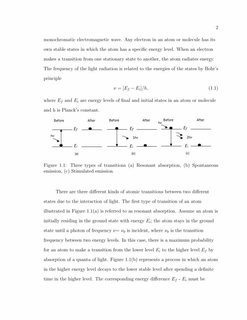
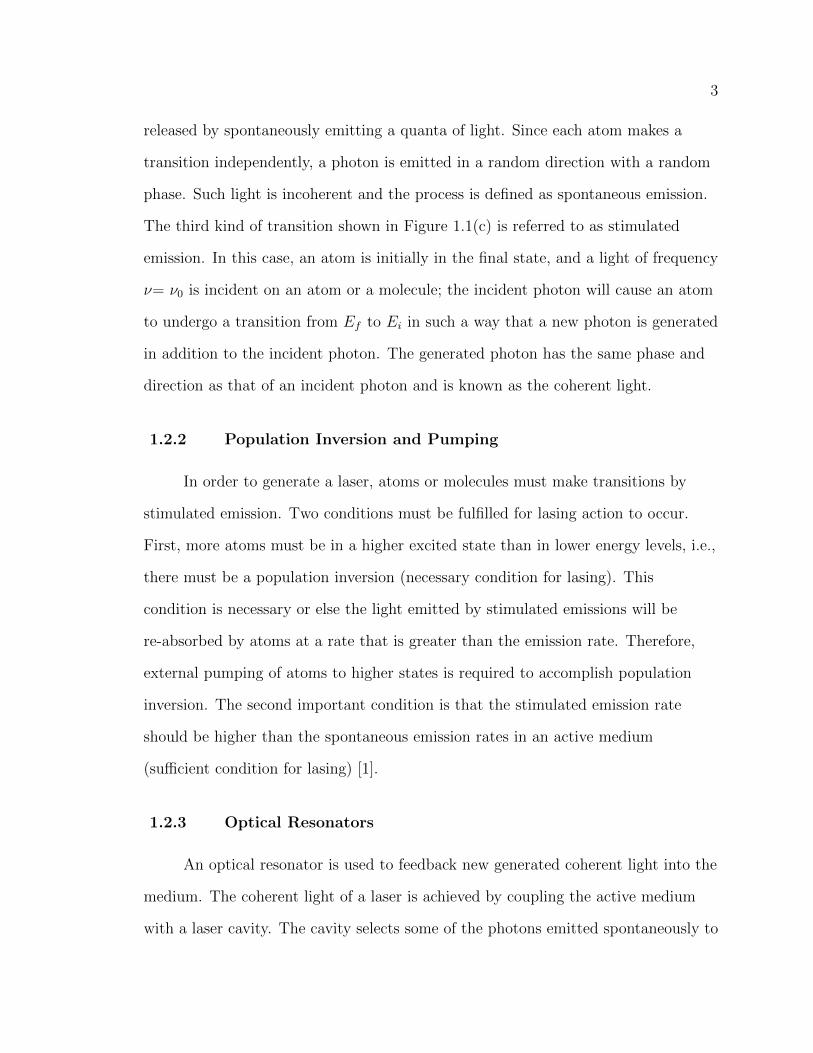
Figure 1.1: Three types of transitions (a) Resonant absorption, (b) Spontaneousemission, (c) Stimulated emission.
There are three different kinds of atomic transitions between two different
states due to the interaction of light. The first type of transition of an atom
illustrated in Figure 1.1(a) is referred to as resonant absorption. Assume an atom is
initially residing in the ground state with energy Ei; the atom stays in the ground
state until a photon of frequency ν= ν0 is incident, where ν0 is the transition
frequency between two energy levels. In this case, there is a maximum probability
for an atom to make a transition from the lower level Ei to the higher level Ef by
absorption of a quanta of light. Figure 1.1(b) represents a process in which an atom
in the higher energy level decays to the lower stable level after spending a definite
time in the higher level. The corresponding energy difference Ef - Ei must be
3
released by spontaneously emitting a quanta of light. Since each atom makes a
transition independently, a photon is emitted in a random direction with a random
phase. Such light is incoherent and the process is defined as spontaneous emission.
The third kind of transition shown in Figure 1.1(c) is referred to as stimulated
emission. In this case, an atom is initially in the final state, and a light of frequency
ν= ν0 is incident on an atom or a molecule; the incident photon will cause an atom
to undergo a transition from Ef to Ei in such a way that a new photon is generated
in addition to the incident photon. The generated photon has the same phase and
direction as that of an incident photon and is known as the coherent light.
1.2.2 Population Inversion and Pumping
In order to generate a laser, atoms or molecules must make transitions by
stimulated emission. Two conditions must be fulfilled for lasing action to occur.
First, more atoms must be in a higher excited state than in lower energy levels, i.e.,
there must be a population inversion (necessary condition for lasing). This
condition is necessary or else the light emitted by stimulated emissions will be
re-absorbed by atoms at a rate that is greater than the emission rate. Therefore,
external pumping of atoms to higher states is required to accomplish population
inversion. The second important condition is that the stimulated emission rate
should be higher than the spontaneous emission rates in an active medium
(sufficient condition for lasing) [1].
1.2.3 Optical Resonators
An optical resonator is used to feedback new generated coherent light into the
medium. The coherent light of a laser is achieved by coupling the active medium
with a laser cavity. The cavity selects some of the photons emitted spontaneously to

4
repropagate through the medium. Neglecting any phase shifts in the cavity, the
allowed wavelength is given by
λn = 2L/n, (1.2)
where L is the length of a linear laser cavity and n is the harmonic mode of the
wave. Thus, the cavity allows only those photons whose wavelength can form a
standing wave in the cavity. This limits the wavelength and direction of the photons
allowed to repropagate through the medium. These photons induce other photons
with the same propagating direction, phase, and wavelength via stimulated
emission, and in a brief time all the photons propagating through the cavity are
coherent. To get this coherent light out of the cavity and make use of it, one of the
reflective ends of the cavity is made semi-reflective, thus, allowing some of the
coherent light to escape. The rate at which the photons are randomly absorbed or
exit through the semireflective ends of the cavity is called transmission loss. This
does not include other losses like absorption or diffraction losses. The rate at which
the photons give rise to other photons via stimulated emission is called gain. To
have a functioning laser, the gain versus overall loss ratio must be greater than one.
Beyond the aforementioned requirement for population inversion, the other two
main requirements for laser operation are an active light-emitting medium and an
optical resonator for regenerating the radiation field [2].
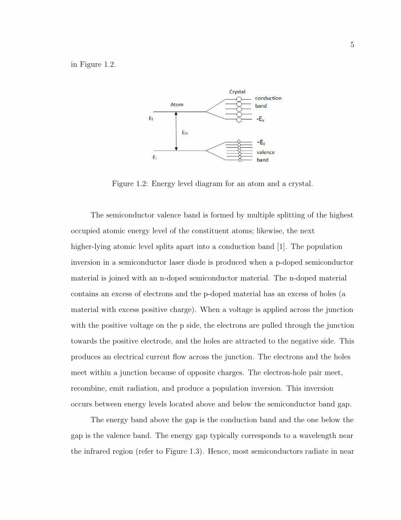
1.3 Semiconductor Laser Diode
A semiconductor laser diode is a specially fabricated p-n junction device that
emits coherent light when it is forward biased. When atoms or molecules come
together into a semiconductor crystal, the discrete atomic energy level smears into
energy bands, which are significantly different from discrete energy levels, as shown
5
in Figure 1.2.
Figure 1.2: Energy level diagram for an atom and a crystal.
The semiconductor valence band is formed by multiple splitting of the highest
occupied atomic energy level of the constituent atoms; likewise, the next
higher-lying atomic level splits apart into a conduction band [1]. The population
inversion in a semiconductor laser diode is produced when a p-doped semiconductor
material is joined with an n-doped semiconductor material. The n-doped material
contains an excess of electrons and the p-doped material has an excess of holes (a
material with excess positive charge). When a voltage is applied across the junction
with the positive voltage on the p side, the electrons are pulled through the junction
towards the positive electrode, and the holes are attracted to the negative side. This
produces an electrical current flow across the junction. The electrons and the holes
meet within a junction because of opposite charges. The electron-hole pair meet,
recombine, emit radiation, and produce a population inversion. This inversion
occurs between energy levels located above and below the semiconductor band gap.
The energy band above the gap is the conduction band and the one below the
gap is the valence band. The energy gap typically corresponds to a wavelength near
the infrared region (refer to Figure 1.3). Hence, most semiconductors radiate in near

6
infrared region and are not transparent in the visible spectral region [3]. The optical
feedback is implemented by reflections, which are usually implemented by cleaving
the semiconductor material along its crystal planes. The refractive index difference
between the crystal and the surrounding air causes the cleaved surfaces to act as
reflectors. Thus, the semiconductor material acts both as a gain medium and a
Fabry-Perot optical resonator [4].
Figure 1.3: Energy bands in semiconductors.
1.4 Basic Characteristics of a Semiconductor Laser Diode
The first continuous wave double heterostructure laser diode operating at
room temperature was demonstrated in 1970 by Zhores Alferov. In this section, we
consider some elementary properties of laser diode characteristics such as threshold
current, output power, beam divergence, and spectral content.
1.4.1 Threshold current and threshold current density
Threshold current is one of the most important basic parameters of laser
diodes. It specifies the degree at which they emit light when current is injected into

7
the devices. As the injected current is increased, the laser first demonstrates
spontaneous emission. The spontaneous emission increases very gradually until it
begins to emit stimulated radiation, which is the onset of laser action. Threshold
current is the exact current value at which this phenomenon takes place. It is
generally desirable that the threshold current be as low as possible, resulting in a
more efficient device. Thus, a threshold current is one measure used to quantify the
performance of a laser diode.
Threshold current is dependent on the quality of the semiconductor material
from which the device is fabricated and the general design of the structure of the
device waveguide. However, it is also dependent on the size and area of a laser
device. One laser diode could demonstrate a much higher threshold current than
another device and still be considered a much better laser. This is because the area
of the device can be large. A laser that is wider or longer requires more electrical
power to reach the onset of laser action than a laser of a smaller area. As a result,
when comparing the threshold current values of different devices, it is more
appropriate to talk about threshold current density rather than threshold current.
Threshold current density is denoted by the symbol Jth and is determined by
dividing the experimentally obtained threshold current value Ith by the
cross-sectional area of the laser gain medium. Threshold current density is one of
the parameters that is a direct indication of the quality of a semiconductor material
from which the device is fabricated. When comparing the performance of various
laser devices, one must compare the threshold current density values rather than the
threshold current values. While calculating the current density of the laser, it is
necessary to accurately measure the area of the laser through which current is being
injected [5].

8
1.4.2 Output Power
Output power is another parameter used to characterize a laser diode.
Figure 1.4 [5] shows an experimental result, which depicts output power of a typical
continuous wave (CW) semiconductor diode laser as a function of injection current
(L-I curve).
Figure 1.4: Output light versus injection current in a semiconductor diodelaser(reprinted with permission from Newport tutorial).
The efficiency of a laser in converting electric power to light power is
determined by the slope of the L-I curve, denoted by the change in output power
over the change in current (∆P/∆I). The inset in Figure 1.4 schematically shows a
broad area (100 µm wide stripe) laser diode emitting radiation from both its front
and back mirror facets. When the forward bias current is low, the laser diode
operates like light-emitting diodes (LEDs) where the carrier density in the active
layer is not high enough for population inversion; spontaneous emission is dominant
in this region. As the forward bias current increases, population inversion occurs.

9
Stimulated emission becomes dominant at a certain bias current as the threshold
current. The injection current above the threshold induces the abrupt onset of laser
action, and coherent light is emitted from the diode laser. The laser’s threshold
current is evaluated by extrapolating the linear part of the L-I curve to zero output
power. If the injection current is increased to excessively high values, the L-I curve
becomes sub-linear. Operation at high current shortens the lifetime and can fatally
damage the laser [1].
1.4.3 Beam Divergence and Astigmatism
Divergence of the output laser beam from a diode laser is described in
Figure 1.5.
Figure 1.5: Structure and lasing mode in a semiconductor laser.
The beam is diffraction-limited in both planes of the junction (orthogonal and
parallel) due to the small size of the laser diode chip. The output of a laser diode is
highly divergent, special collimating optics are often used since many applications
require collimated light. Either molded spherical or multiple element glass lenses are
used to collimate the output. These lenses typically have a numerical aperture of

10
0.5 or better to collect the entire laser output beam. Using lenses, the output light
of a laser diode can be formed into a collimated beam with little divergence. If a
gain-guided laser diode beam is collimated or being focused, then a cylindrical lens
is used to account for astigmatism. Astigmatism is a condition in which the
apparent focal points of the two axis do not coincide. It limits the ability to focus
the laser beam into a small spot size and complicates focusing the output beam to a
sharp well-defined point. A long focal length lens is used to compensate for the
astigmatism and then the collimating lens can provide a beam that has little
divergence in both axis [5].
1.4.4 Optical Spectrum
The optical spectrum of a laser diode depends on particular characteristics of
the laser’s optical cavity.
Figure 1.6: Multimode versus single mode spectra (reprinted with permission fromNewport tutorial).
Most conventional gain or index-guided devices have a spectrum with multiple
peaks, whereas distributed feedback (DFB) and distributed-Bragg-reflector (DBR)

11
type of devices display a single well-defined spectral peak. Figure 1.6 [5] shows a
comparison between these two spectral behaviors. The number of spectral lines that
a laser is capable of supporting is a function of the cavity structure, as well as
operating current. The result is that the multimode laser diodes exhibit spectral
outputs with multiple peaks around their center wavelength.
Figure 1.7: Geometry of a linear laser cavity.
The optical wave propagating through the laser cavity forms a standing wave
between the two mirror facets of the laser. The distance L between the two mirrors
determines the period of oscillation of this curve. This standing optical wave
resonates only when the cavity length L is an integer number m of half wavelength
existing between the two mirrors. In other words, a node must exist at each end of
the cavity. The only way this can take place is for L to be exactly a whole number
multiple of half wavelength λ/2, where λ is the wavelength of light in a
semiconductor material and is related to the wavelength of light in free space λ0
through the index of refraction n by the relationship λ= λ0/n. As a result of this
situation, there can exist many longitudinal modes in the cavity of a laser diode,
each resonating at its distinct wavelength of λm=2L/m . From this, we can note

12
that two adjacent longitudinal laser modes are separated by a wavelength
∆λ = (λ0)2/2nL. (1.3)
1.4.5 Center Wavelength Change with Temperature
There is a linear relationship between temperature and center wavelength. As
temperature increases, the center wavelength of the laser diode also increases. This
characteristic is useful in spectroscopy applications, laser diode pumping of solid
state lasers, and erbium-doped fiber amplifiers, where the wavelength of emission of
the laser diode can be accurately temperature-tuned to the specific properties of the
material with which it is interacting [5].
1.4.6 Mode Hopping
The short continuous segments in Figure 1.8 [5] indicate the tuning of the
optical length of a cavity for a given longitudinal mode. When the peak of the gain
medium has shifted too far, the laser jumps to another mode. This is indicated by
the breaks in the curve.
Figure 1.8: Mode hopping observed while temperature tuning a laser diode (reprintedwith permission from Newport tutorial).
Single-mode lasers exhibit this phenomenon called mode hopping, in which
13
the center frequency of the laser diode hops over discrete wavelength bands and
does not show continuous tuning over a broad range. One can change the
wavelength where the discontinuities take place by making small adjustments to the
drive current. When selecting a specific laser diode for an application requiring a
specific wavelength such as spectroscopy, mode hopping must be taken into account
while temperature tuning the device.
1.5 Types of Semiconductor Diode Laser
There are many types of diode lasers. Each type of diode laser has its own
features and by choosing the correct type of diode laser for the given application,
the right performance can be obtained. Some of the main types of diode lasers
include the following:
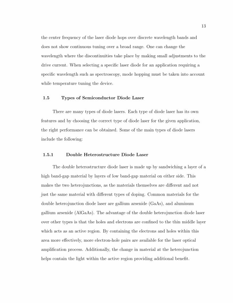
1.5.1 Double Heterostructure Diode Laser
The double heterostructure diode laser is made up by sandwiching a layer of a
high band-gap material by layers of low band-gap material on either side. This
makes the two heterojunctions, as the materials themselves are different and not
just the same material with different types of doping. Common materials for the
double heterojunction diode laser are gallium arsenide (GaAs), and aluminum
gallium arsenide (AlGaAs). The advantage of the double heterojunction diode laser
over other types is that the holes and electrons are confined to the thin middle layer
which acts as an active region. By containing the electrons and holes within this
area more effectively, more electron-hole pairs are available for the laser optical
amplification process. Additionally, the change in material at the heterojunction
helps contain the light within the active region providing additional benefit.

14
1.5.2 Quantum Well Diode Laser
The quantum well diode laser uses a very thin middle layer; this acts as a
quantum well where the vertical component of the electron wave function is
quantized. As the quantum well has an abrupt edge, this concentrates electrons in
energy states that contribute to laser action, which increases the efficiency of the
system. In addition to the single quantum well lasers, multiple quantum well lasers
also exist. The presence of multiple quantum wells improves the overlap of the gain
region with the optical waveguide mode.
1.5.3 Quantum Cascade Diode Laser
A quantum cascade diode laser is a form of heterojunction laser in which the
difference between well energy levels is used to provide laser light generation. This
allows the laser diode to generate relatively long wavelength light. The actual
wavelength can be adjusted during fabrication by altering the laser diode layer
thickness.
1.5.4 Separate Confinement Heterostructure Diode Laser
This type of diode laser has been widely used for the majority of diode lasers
since 1990s. The separate confinement diode laser overcomes the problem that
exists in many other forms of diode laser, the thin laser layer is too thin to confine
the light effectively. This laser overcomes the problem by adding another two layers
with a lower refractive index on the outside of the existing ones. This effectively
confines the light to within the diode.

15
1.5.5 Other Types of Diode Lasers
Distributed feedback diode lasers (DFB), are used in forms of
telecommunications or data transmission using optical systems. Here the laser diode
wavelength is important, but laser diodes are not particularly stable in this respect
with wavelength varying with temperature, voltage, ageing, etc. A diffraction
grating is etched close to the p-n junction of the diode to assist in stabilizing the
wavelength of the generated light signal. This grating acts like an optical filter
causing a single wavelength to be fed back to the gain region. The pitch of the
grating is set during manufacture, and it only varies slightly with temperature.
Vertical-cavity surface-emitting diode lasers are a form of surface emitting
laser and they emit the laser radiation in a direction perpendicular to the substrate,
delivering a few milliwatts with high beam quality [6].
External cavity diode lasers contain a laser diode as the gain medium of a
longer free space cavity (extended cavity). These lasers are often
wavelength-tunable and they exhibit a small emission spectral linewidth. We
characterize and study this type of diode laser in this thesis.
16
CHAPTER 2
EXTENDED CAVITY DIODE LASER
2.1 Introduction
The first experiment on a laser diode coupled to an external cavity was
performed by Crowe and Craig in 1964 [7], soon after the first successful operation
of a diode laser. With the development of semiconductor diode lasers, tunable
extended cavity diode lasers are finding a wide variety of applications in a broad
range of fields. They are of considerable interest in coherent optical
telecommunications, atomic and molecular laser spectroscopy, precise
measurements, and environmental monitors. An overview of the most important
applications is outlined as follows:
• Optical coherent telecommunications: Drop-add multiplexers,
elimination of wavelength blocking, easy use of optical core.
• Sensing: Ultra-high resolution spectroscopy, optical radar, atmospheric and
environmental studies, industrial processing monitoring.
• Precise measurements: Atomic clock and magnetometer, optical
spectrum analysis, device characterization.
In addition to the typical applications exemplified above, there are many other
applications, including nonlinear optical conversion, optical data storage, coherent
optical transient processing, and quantum optical manipulation and engineering [1].
Tunable diode lasers are widely used in atomic physics. This is primarily because

17
they are reliable sources of narrow band (< 1 MHz) light and are vastly less
expensive than traditional tunable dye or Ti-Sapphire lasers. However, the
frequency tuning characteristics of the light from a diode laser are far from ideal,
which greatly reduces its utility. In particular, the laser output is some tens of
megahertz wide and can be continuously tuned only over certain limited regions.
These characteristics can be improved by the use of optical feedback to control the
frequency of the laser [8]. There are many possible techniques for the wavelength
tuning of semiconductor diode lasers. One of the practical approaches is tunable
external cavity diode lasers (ECDLs), that could provide an alternative to
monolithic semiconductor diode lasers for accomplishing the wide tuning of a diode
laser [1].
2.2 Design of an Extended Cavity Diode Laser
In designing an external cavity diode laser system, a few elementary concerns
must be taken into consideration. We need to maximize the feedback, to precisely
align the laser cavity, to select the wavelength, and to accurately control the laser
chip temperature and extract the excess heat [9]. A tunable external cavity diode
laser system consists primarily of a semiconductor diode laser with or without
antireflection coatings on one or two facets, a collimator for coupling the output of
the diode laser, and an external mode-selection filter. In general, the features of a
diode laser in an external cavity can change greatly depending on the length of the
external cavity, feedback strength, optical power, and diode laser parameters.
Littman-Metcalf configuration and Littrow cavity configuration (Figure 2.1) are
typical examples of ECDL sources in which gratings are used to provide optical
feedback, select single-mode operation, and tune the wavelength over the whole

18
range of gain bandwidth by changing the grating position and orientation [1].
Figure 2.1: Tunable external cavity diode laser with (a) Littrow and (b) Littmanconfiguration.
2.2.1 Littrow Cavity Configuration
The frequency of the tunable laser diode is very sensitive to changes in
temperature and injection current, and has large linewidths (∼100 MHz) and poor
tunability. It is well known that these shortcomings can be rectified by operating
the laser in a longer external cavity which provides frequency-selective optical
feedback. A particularly simple implementation of this idea uses feedback from a
diffraction grating mounted in a Littrow conguration (refer to Figure 2.2).
In a Littrow configuration, first-order light which is diffracted from a grating
is coupled back into the laser diode, and the directly reflected light forms the output
beam [10]. The formula for constructively diffracted orders of light reflected from a
diffraction grating is:
d sin θ = mλ, (2.1)
where d is the spacing between the grooves, θ is the angle of incidence, λ is the
wavelength of the incident light, and m is an integer. One consequence of the above
equation is that spectra diffracted off a grating are reproduced at several different

19
angular positions about the grating [2].
Figure 2.2: Littrow configuration set up.
The various replications of the spectra are called orders of diffraction and
obey the grating equation:
(sin θi + sin θm) = mλ/d, (2.2)
where θm is the angle of the mth order diffracted beam, θi, m and λ are incident
angle, an integer, and wavelength. The Littrow angle (when θm= - θi) is determined
from the grating equation 2.2. If we define θL as the angle of incidence, then the
equation for the Littrow angle of the system becomes:
2d sin θL = mλ. (2.3)
This particularly simple and effective configuration can be used with a blazed
grating to reduce feedback and increase output power, thus improving overall
efficiency. This configuration is analogous to the addition of standing waves on an
oscillating rope. Littrow configuration is made possible with the implementation of
blazed gratings (refer to Figure 2.3).
Blazing is a technique of shaping individual grooves of a diffraction grating so
that the diffraction envelope maximum shifts into another order. While the

20
diffraction envelope is shifted by the shaping of the individual grooves, the
interference maxima remains fixed in position. Their positions are determined by
the grating equation(2.2), in which angles are measured relative to the plane of the
grating. The result is that the diffraction maxima now favor a principal maximum
of higher order (|m|>0) and the grating redirects the bulk of the energy in that
particular order [11].
Figure 2.3: Blazed grating.
2.3 Components and Parts of an ECDL
We have built an extended cavity diode laser of the design mentioned by
Arnold, Boshier and Wilson [10], [8]. It is an effective method with inexpensive
components that helps in reducing the linewidth and improving the wavelength
tunablity of a diode laser. This design has three basic components, a commercial
diode laser, a diffraction grating, and a collimating lens. These components are
mounted on a base plate. The laser and lens are mounted in such a way that the
lens can be carefully positioned relative to the laser to ensure proper collimation.

21
The diffraction grating is mounted in the Littrow configuration. The emission
wavelength can be tuned by rotating the diffraction grating. The grating serves as
one end mirror of the laser cavity with the back facet of the diode providing the
second mirror. In order to tune the frequency of the laser, we must change the
length of the cavity in a properly controlled manner. This can be done by a piezo
electric transducer stack/disk (Thorlab model- AE0203D04F) attached to the
grating that moves the grating in response to applied voltage.
Figure 2.4: Extended Cavity Diode Laser (ECDL) set up.
Figure 2.4 displays our experimental setup of an ECDL. Our design uses
various low cost commercial components. We have used a Sanyo DL7140 201S
infrared laser diode emitting light of wavelength 785nm (typically). A collimation
tube (Thorlab) holds the laser diode and the collimating lens. The optical output of
the laser diode is very divergent with a beam divergence of 7(FWHM) in parallel
and 17(FWHM) in perpendicular directions, so we need to use a lens close to the

22
laser facet to collimate the output. We also use a Thorlab holographic diffraction
grating GH13-12V with 1200 lines per mm. Most of the light is directly reflected by
the grating (m=0 order), but roughly 20% is reflected back into the laser (m=1
order). The grating forms an external cavity (i.e., external to the laser’s own
internal semiconductor cavity), which serves to frequency-stabilize and line-narrow
the laser output. With the simple addition of a diffraction grating, the laser is now
less sensitive to stray light feedback, and its linewidth is reduced to ∆ν< 1 MHz,
much smaller than the atomic transition linewidths we will be observing.
The injection current necessary to run the laser is provided by the low noise
current driver (Thorlab LDC 1100). A thermoelectric Peltier cooler (TEC)
maintains the laser diode at a set temperature by actively cooling or heating the
entire mechanical setup. In order to ensure that the entire laser setup is at the same
temperature, all laser components have been polished to have maximum surface
contact between them. We also use heat-conducting thermal paste to optimize
thermal conductivity. The TEC is driven by a proportional-integral-derivative
controller (PID controller-model-XMT 700). It is a generic control loop feedback
mechanism widely used in industrial control systems. The PID temperature
controller stabilizes the temperature of a laser to the set temperature within
approximately 0.5 Celsius. The TEC is sandwiched between two conductive
aluminum plates at the base of the laser mount and is coupled to a thermistor
Pt100 (a Platinum100 resistor whose resistance varies with temperature). The
thermistor buried inside the laser mount (not visible in Figure 2.4), serves as a laser
temperature sensor for the PID controller. The entire laser setup is mounted on an
aluminum block which serves as a large heat sink. The block is mounted stably on
an optical table, providing vibrational and mechanical stability, dampening and an
additional heat sink.

23
2.4 Operating Principle of an ECDL
To operate an extended cavity diode laser, we connect the laser diode with the
laser diode current controller (LDC) by checking the polarities of the current driver
and the laser diode. We slowly increase the current in the diode until lasing is
observed (sudden increase in the brightness of the output as viewed by a fluorescent
card used to visualize the presence of IR radiation). The power builds up in a laser
diode and above threshold, the power increases proportionally to the difference
between the current and the threshold value (Figure 1.4). Above threshold, there is
adequate population inversion such that stimulated emission is dominant. When
ramping the diode, we take caution and do not change the current too abruptly, for
the laser is very sensitive to surges or transient currents. We are also careful not to
exceed the laser diode’s maximum operating current i.e., 100 mA [12].
The output laser beam is elongated and divergent. We rotate the collimation
tube in the laser mount until the long axis of the beam is horizontal. The laser is
linearly polarized along the long axis of the facet and the laser output is roughly
Gaussian. The laser output is collimated by adjusting the position of the lens with a
wrench i.e., the lens is on a threaded mount that can have its position adjusted by
rotating the lens holder. The laser diode should be exactly one focal length away
from the collimating lens. In practice, the best way to see if the laser is at the focal
point of the lens is to remove the back half of the ECDL, which is the diffraction
grating and mount, and aim the entire laser housing at a distant wall. Now we see if
the size of the output beam on the wall is of the same size as that observed when
shining the laser on a piece of paper placed right in front of the setup. It is possible
for us to have an agreement in the size of the light beam on the wall and that of the
beam on the piece of paper and still have the output not collimated. Therefore, we

24
examine the spread of the laser beam on the piece of paper, when the paper is at
several different points between the laser diode and the wall. If the size of the
spread is constant regardless of the position of the paper, then the laser is
collimated. Aside from being collimated, it is also desirable to have the output from
the laser level with the horizontal plane. The laser beam must be horizontal so that
the first order diffracted beam will be directed back at the collimating lens rather
than above or below it [2].
2.5 Alignment of an ECDL
The following methods are used to align the grating with respect to the laser
output, such that the Littrow condition stated before can be satisfied. Due to the
fact that the aperture of the lasing chip is 0.1 mm by 0.3 mm, physically positioning
the grating based on simple geometry is not practical [12]. Therefore, we employ a
pin-hole method followed by a current scanning method to align the grating and
check for optical feedback.
First, we stabilize the temperature of the laser diode mount at 66 Fahrenheit.
As illustrated in Figure 2.5, the output light from the laser diode is incident on the
grating, and the diffracted light gets reflected from the mirror, M2, attached parallel
to the grating. The beam 1 coming out from the optical set up is made to
retro-reflect from an external mirror, M1, placed in front of the mount. This is
checked by a small piece of paper (with a pin hole) placed in front of the laser beam
coming out of the mount. If the reflected spot from the external mirror is seen
above or below the pin hole, we adjust the alignment of the external mirror, M1,
until the laser beam is retroreflected (beam 2), so the reflected spot coincides with
the pinhole (incident beam). Then, we adjust the orientation of the grating with the

25
help of vertical and horizontal actuators (not shown in Figure 2.5) so that the light
(beam 3) sent back into the optical set-up is retroreflected back towards the pinhole
and passes through it a third time. Injecting light back into the laser from the
grating gives rise to a buildup of light at a frequency determined by the external
cavity, leading to preferential lasing on this mode and concomitantly a reduction in
the laser threshold. Observing the change in the laser threshold therefore provides
another way to align the grating using the current scanning technique.
Figure 2.5: Pin hole alignment technique, G: grating, P: piece of paper with a pinhole, M2: mirror attached inside the mount parallel to the grating, M1: externalmirror, LD: laser diode.
In the current scanning technique, we monitor the laser output using a power
meter or a photodiode. After crudely aligning the grating, we operate the laser at a
current close to threshold. Then we modulate the laser current with a saw tooth
waveform from the frequency generator (10 hz). If the laser power is then monitored
on a photodiode and displayed on an oscilloscope in X-Y mode (refer to Figure 2.6
showing the detected power as a function of the current level), we get a real time
monitor of the laser threshold (i.e., the knee in power that is recorded when
measuring the output power versus current for the bare diode). Alignment of the
grating then shifts the position of this knee and the optimum injection is found,
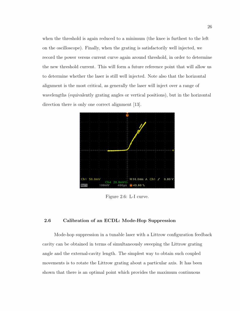
26
when the threshold is again reduced to a minimum (the knee is furthest to the left
on the oscilloscope). Finally, when the grating is satisfactorily well injected, we
record the power versus current curve again around threshold, in order to determine
the new threshold current. This will form a future reference point that will allow us
to determine whether the laser is still well injected. Note also that the horizontal
alignment is the most critical, as generally the laser will inject over a range of
wavelengths (equivalently grating angles or vertical positions), but in the horizontal
direction there is only one correct alignment [13].
Figure 2.6: L-I curve.
2.6 Calibration of an ECDL: Mode-Hop Suppression
Mode-hop suppression in a tunable laser with a Littrow configuration feedback
cavity can be obtained in terms of simultaneously sweeping the Littrow grating
angle and the external-cavity length. The simplest way to obtain such coupled
movements is to rotate the Littrow grating about a particular axis. It has been
shown that there is an optimal point which provides the maximum continuous

27
tuning range [14]. This concept is discussed later on in detail with Figure 2.8. It is
possible to tune a laser wavelength in a wide range of 240 nm near 1450 nm with an
external cavity diode laser with mode-hops [15]. However, a continuous tuning
range of 15 nm around 1300 nm without mode hop has been achieved with the same
type of ECDLs and a simple mechanical arrangement [16].
In such lasers, the grating angle controls the wavelength λr associated with
minimum losses. Nevertheless, the lasing wavelength also depends on the cavity
length that determine resonant mode positions. Continuous tuning is obtained if the
resonant wavelength λq of the longitudinal mode number q and the minimum loss
wavelength λr are spectrally shifted at the same rate to keep the lasing mode in a
low-loss region. This condition can be fulfilled by the use of a rotation-translation
combination of the grating positions. Despite the complex mechanical setup and
stability requirements, we can tune a single-mode laser by moving the grating. To
understand how the laser frequency changes when the grating is moved, we have to
examine several cases [17].
Figure 2.7: Different ways to move the grating and the corresponding change inwavelength.
28
In Figure 2.7(a), the grating is moved along the laser beam direction, the
standing wave oscillating inside the cavity will be stretched, resulting in a
continuous tuning of frequency. But as the frequency changes, this stretching also
varies the diffraction angle from the grating. After a while, a mode with one more
half-wave period inside the cavity will point directly towards the mirror; i.e., the
mode will have low losses, leading to an abrupt mode hop back in frequency as
shown in the right side of Figure 2.7(a). If, however, the grating is moved
perpendicular to the beam, as illustrated in Figure 2.7(b), the distance between any
particular groove on the grating and the mirror does not change. This means that
even though the cavity is becoming longer, there is no change in the frequency of
the light diffracted back in to the laser. We can also vary the frequency of the laser
by changing the angle of the grating, thereby, choosing the frequency feedback to
the laser. If the grating is turned around the center point of the beam, as shown in
Figure 2.7(c), the frequency of the cavity at the middle of the beam will not change.
This means that there is no variation of frequency until the next possible mode has
lower losses, and then the laser mode hops to the new frequency. In order to achieve
continuous tuning with no mode hops, the grating has to be translated and rotated
in a coordinated way. It is possible to use grating rotation only to optimize the exact
position of the rotation axis and to obtain optimum continuous wavelength tuning.
In Figure 2.8, the intersection of the laser axis and the grating plane is
denoted by G. The origin of the axis is at point O, OG=L, where L is the optical
length of the laser cavity. The first order diffraction of the grating is reflected back
to the cavity at a grating angle θ. For a grating period d, λr is given by:
λr = 2d sin θ. (2.4)
Taking into consideration the grating translation in its plane, the resonant cavity

29
mode wavelength λq (refer to equation 1.2) is given by a well known equation:
λq = 2L/q, (2.5)
It is assumed that the grating is rotated about a point R in such a way that the
mode frequency λq is exactly at the minimum-loss frequency λr. So equating 2.4
and 2.5 gives:
sin θ = L/qd. (2.6)
From Figure 2.8, we get sinθ = L/P . Therefore, the condition for mode-hop
suppression is satisfied if the distance P = qd. In other words, the optimum rotation
point that provides continuous tuning is the point R as indicated in Figure 2.8.
Figure 2.8: Schematic diagram of laser configuration showing optimum rotation pointR, LD: laser diode, G: grating.

30
CHAPTER 3
FREQUENCY TUNING PARAMETERS OF THE ECDL
3.1 Introduction
The tuning parameters presented in this chapter control the frequency output
of our laser. At the level of precision that we need for our experiment, the laser is
not adequately stabilized. So we are continuously adjusting these tuning parameters
so that the laser frequency does not deviate from a stable reference frequency
(atomic spectrum).
3.2 First Tuning Parameter- Temperature
Thermal expansion changes the cavity length of a semiconductor chip in a
laser diode. An increase in temperature increases the cavity length and so the
resonant wavelength. It also shifts the semiconductor gain peak towards longer
wavelengths (shorter frequencies). The laser frequency can be changed by changing
the temperature of the laser. The temperature of a laser diode may be adjusted
externally. We can vary the temperature from 0C to 40C, and a typical
temperature tuning is 0.03 nm/C, or 15GHz/C. The advantage of using this
tuning parameter is that large changes in frequency are possible. However, there are
some disadvantages. First, it can take up to half an hour for the temperature of the
laser to stabilize completely. Second, it is very difficult to make small changes in
laser frequency, so the tuning that can be achieved is very coarse [18].

31
3.3 Second Tuning Parameter- Injection Current
The injection current alters the temperature of a laser through Joule heating:
PLD=IR2∼mc∆T , where R is the effective resistance of the lasing chip, I is the
injection current, m and c are effective mass and specific heat capacity of the laser
diode. Altering the injection current is a simple way of indirectly changing the
temperature. The injection current also increases the carrier density within the
lasing medium, which affects the refractive index. However, once the injection
current reaches the threshold, carrier density is clamped and the injection current
has command of the laser through temperature only. Unlike direct temperature
control, which is usually accomplished externally, injection current raises the laser
temperature internally and thus elicits a much faster response from the laser. A
typical frequency tuning rate for the injection current is approximately 4 GHz/mA.
The injection current is a tuning parameter that shifts both the lasing cavity modes
and the gain profile simultaneously, and at different rates, producing a staircase
mode hopping tuning curve mentioned in chapter 1 (refer to Figure 1.8). The power
output of the laser depends linearly on the injection current beyond the threshold
current. The power is given by:
P0 = nex(hν/e)(I − Ith), (3.1)
where nex is the differential external quantum efficiency which is equal to the flux
per unit change of current above threshold and Ith is the threshold current value. In
this way the injection current not only changes the laser diode temperature but also
changes the output power. The power versus current curve is an important
characteristic of a laser and should be among the primary measurements made. It
should also be noted that the entire power versus current curve is shifted by a
constant amount as the temperature is altered, such that: Ith(T ) is proportional to

32
exp(T/T0), where T0 is the characteristic temperature of the laser diode material.
The curve shifts by about 0.4 mA/0C for a typical diode laser [12].
3.4 Third Tuning Parameter- Grating Optical Feedback
The light emitted by the laser diode strikes a grating. The grating reflects a
narrow frequency range back into the laser, forcing the laser to emit light within
that particular frequency range. By changing the angle of the grating with respect
to the incoming light, different frequencies may be sent back into the laser, making
it possible to tune the laser to a particular frequency range. The grating is mounted
on a custom made aluminum piece which is attached to the modified movable
commercial mount displayed in Figure 2.4. The movable commercial mount is
attached to the fixed laser mount, but it can be rotated. Adjustable screws are used
to coarsely adjust the grating angle by pushing on the modified mount.
Fine adjustment is achieved by a piezoelectric transducer (PZT) which is
sandwiched between the laser mount and the modified mount holding the grating.
The PZT stack, made up of ceramic material, expands in response to an applied DC
voltage (as high as 150V) provided by a PZT driver. The expansion of the PZT is
proportional to the applied voltage. Voltage applied to the PZT changes its
thickness, thereby causing the modified mount to move, changing the angle of the
grating relative to the laser light. Figure 3.1 displays the working of the PZT which
is placed behind the grating.
Depending on the voltage on the piezo element, the angle φ changes, thereby
changing the wavelength. As with laser current, this tuning parameter allows for
fine frequency adjustment. For every volt that is applied to the PZT by the PZT
driver, the frequency of the laser can be changed. This tuning parameter also elicits

33
a faster laser response than the thermo-electric cooler [18].
Figure 3.1: Tuning the wavelength with the grating.
3.5 Data Collection and Analysis
In our set up, a Mach Zehnder interferometer with mismatched arm lengths is
used to determine the frequency drift of the diode laser with the change in the
injection current and PZT voltage.
3.5.1 Mach Zehnder Interferometer
The Mach Zehnder interferometer was developed by physicists Ludwig Mach
and Ludwig Zehnder. It uses two separate beam splitters (BS) to split and
recombine the beams and give two output beams, which can be sent to
photodetectors. The optical path length in the two arms may be identical or
different (i.e., with an extra delay line). The distribution of optical power at the two
outputs depends on the precise difference in optical arm lengths and on the
wavelength (optical frequency) of the beam. If the interferometer is well aligned, the
path length difference can be adjusted (i.e., by slightly moving one of the mirrors)
so that for a particular optical frequency, the total power goes into one of the
outputs. For misaligned beams (i.e., with one mirror being slightly tilted), there will

34
be some fringe patterns in both outputs, and variations of the path length difference
affect mainly the shape of these interference patterns, whereas the distribution of
total power on the outputs may not change very much [19].
We are using a Mach Zehnder interferometer with arm lengths mismatched to
determine the change in the frequency of the ECDL with tuning parameters (current
and PZT). The set up of the Mach-Zehnder interferometer is shown in Figure 3.2.
Figure 3.2: Mach Zehnder interferometer set up, LD-laser diode, BS-beam splitter,L-Lens, M-mirror, PD-photodiode, OSC-oscilloscope, CCD-Camera.
The light beam from the laser diode is divided into two beams by the beam
splitter BS1. One beam goes to mirror M2 and after reflecting from mirrors M3 and
M4, it reaches beam splitter BS2. The other beam gets reflected by mirror M1. The
two beams recombine at the beam splitter, BS2 after travelling distances D1 and
D2. Here the distance D1 is 80 cm and D2 is 4 m. The lenses, L1 of focal length 20
cm and L2 of focal length 100 cm, are placed midway between the two interfering
beam paths. They are used for proper mode matching of the beams. Another lens

35
L0 of focal length 25 cm is placed between the laser and the beam splitter BS1. The
two interfering beams will have phase difference (due to the path difference) given
by:
φ1 − φ2 = 2π(D2−D1)/λ = ν2π(D2−D1)/c, (3.2)
Here ν is the laser frequency and (D2 -D1) is the path difference between the two
beams. The frequency of the laser is not fixed, rather it is swept by the triangular
waveform applied to the laser diode current controller. Hence as the laser frequency
changes, the phase difference will change. The changes in frequency and phase are
expressed by writing the equation given above as:
∆(φ1 − φ2) = 2π(∆ν)(D2−D1)/c. (3.3)
The intensity of the two superimposed waves, aside from a constant of
proportionality, is given by I=EE*
I = (E1e2iπ(D1/λ−ν/t) + E2e
2iπ(D2/λ−ν/t))(E1e2iπ(D1/λ−ν/t) + E2e
2iπ(D2/λ−ν/t))∗ (3.4)
or I= |E1|2 + |E2|2 + 2E1E2cos[∆(φ1 - φ2)], where ∆ is inserted to indicate the
change in phase from sweeping the frequency. The interference is maximum,
whenever:
∆(φ1 − φ2) = 2nπ. (3.5)
where n is an integer, substituting Eq. (3.5) into (3.3) yields the frequency spacing
of the interference maxima given by:
∆ν = c/(D2−D1), (3.6)
here c= 3x10⁸ m/s and (D2 - D1) = 3.2 m; after solving we get ∆ν= 93.7 MHz.
There are a few factors to consider in order to get good fringes from the
interferometer. First, we should not be misled by weak fringes obtained from
36
interference of the beams reflecting off the two sides of the beam splitter as they will
not have the correct spacing. Second, we need to realize that in order to get good
fringes, the two beams must not only overlap at the photodiode, but they must also
be parallel. The larger the angle between the beams, the closer will be the spacing
of the fringes. As we adjust the beams to be parallel (but still overlapping), the
spacing between the dark fringes will become larger until it is as large as the
photodiode, and we see a large modulation in the photodiode output by changing
the frequency. Often the easiest way to get good fringes is to first make the beams
as parallel and overlapping as possible. Then we make the final adjustments by
looking at the photodiode output and aligning the beams to get the largest fringes
as we ramp the laser frequency [19].
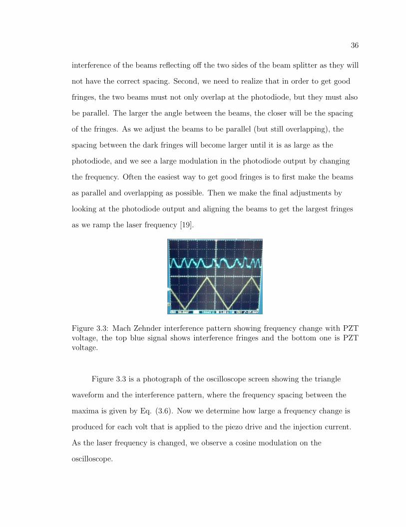
Figure 3.3: Mach Zehnder interference pattern showing frequency change with PZTvoltage, the top blue signal shows interference fringes and the bottom one is PZTvoltage.
Figure 3.3 is a photograph of the oscilloscope screen showing the triangle
waveform and the interference pattern, where the frequency spacing between the
maxima is given by Eq. (3.6). Now we determine how large a frequency change is
produced for each volt that is applied to the piezo drive and the injection current.
As the laser frequency is changed, we observe a cosine modulation on the
oscilloscope.

37
Figure 3.4: Mach Zehnder interference pattern seen through a CCD camera.
According to Eq.( 3.4), we observe the change in intensity of the interference
pattern due to variation in current and PZT voltage. By counting the number of
fringes in a half-waveform as measured on the oscilloscope and multiplying this
number by ∆ν, we will get the total frequency shift per unit volt. However, if we
make a large sweep, we see sudden jumps in the signal as if the phase has abruptly
changed. What has actually happened is that the laser has jumped to a different
frequency (so called “mode hop” as was discussed in the chapter 1). The frequency
where the laser jumps will move, if we change the laser current. Under ideal
conditions, with this laser setup, we can get a scan of about 8 GHz without a
mode-hop. More typically we can get continuous scans (no mode hops) of 3 or 4
GHz. If the frequency range over which we get a continuous scan is shorter than
this, it probably means that the vertical alignment is off. The length of continuous
scan can also be affected by the laser temperature. We also used a CCD camera to
observe the interference pattern. Figure 3.4 displays the interference pattern
through the CCD. Table 3.1 and 3.2 shows the data that we collected.

38
Table 3.1: Frequency drift versus injection current.
LDC current (mA) No. of fringes in 7 mAamplitude waveform
Total frequency shift (GHz/Volt)
36 25 15.646 28 17.556 26 16.266 27 16.976 25 15.686 16 1096 23 14.4
Table 3.2: Frequency drift versus PZT Voltage.
PZT Stack Voltage (Volt) No. of fringes in1 Volt amplitudewaveform
Total frequency shift (GHz/Volt)
3 13 0.22315 16 0.10022 14 0.05835 15 0.04042 16 0.03556 14 0.02369 13 0.01774 13 0.01685 11 0.01292 12 0.012

39
CHAPTER 4
ATOMIC SPECTROSCOPY- RUBIDIUM CELL
4.1 Introduction
Atomic transitions can offer a good frequency reference over a wide
wavelength range and a stable frequency reference under various environmental
conditions like fluctuating temperature, varying pressure, and strain. Transitions
between hyperfine energy levels of the alkali atom rubidium are used as a frequency
reference in our experiment.
4.2 Basic Concept of Frequency Stabilization
The output frequency of an external cavity diode laser depends upon injection
current and temperature. To obtain a stable frequency output, it is important to
stabilize the diode’s temperature and injection current. In a laser diode with
Littrow configuration, the optical feedback from the grating is spectrally narrowed
and peaked at a frequency that can differ from the central frequency of the
free-running diode laser. The feedback narrows the laser linewidth from 50 MHz to
less than 1 MHz. The central frequency will be very close to that of the feedback
signal. Many experiments require a laser with a well-defined frequency. But over
time, the central frequency of a diode laser with grating feedback will drift; this
drift is caused by fluctuations in temperature, injection current, and mechanical
conditions. Stabilizing the laser by locking it to an external reference reduces this
drift. Laser frequency stabilization is based on the generation of a frequency error
signal, which passes through zero at the locking frequency. To achieve the frequency

40
stabilization of a diode laser, a portion of the output diode laser beam is compared
with a frequency reference, an error signal is generated which is then converted into
an electrical signal and feedback to a diode laser after amplification if necessary[18].
There are a variety of reference frequencies which can be used to stabilize the
frequency of a diode laser. In order to stabilize the frequency of our laser, we need a
highly stable optical reference frequency. The hyperfine atomic transitions of the
rubidium-85 isotope provides the level of stability that we need. We use a technique
known as saturated absorption spectroscopy to produce a spectrum of narrow peaks
to which we can lock the frequency of the laser by means of the feedback circuit.
These peaks correspond to different hyperfine transitions of Rb85. By carefully
adjusting the laser temperature, injection current, and grating angle as described in
Chapter 3, we can tune our laser to one of these hyperfine atomic transitions. Our
optical setup is divided into two main parts: a laser frequency monitoring section
and a Doppler-free or saturated absorption spectroscopy apparatus.
4.3 Monitoring the Laser Frequency
After the grating is aligned and the injection is optimized, it is unlikely that
our laser operates at a wavelength coincident with an atomic transition. Tuning the
wavelength so that the laser is on transition requires adjustment of the vertical
actuator together with the laser current and temperature. We direct some or the
entire laser output beam through an atomic vapor cell and observe the cell with an
infrared viewer. We expect to see the fluorescence when the laser is resonant with
an atomic transition [13]. If we fail to tune through an atomic resonance, we employ
an optical spectrum analyzer (model MS9001B/B1) that will reveal the absolute
operating wavelength (nominally 780 nm) of the laser output directly to about +/-

41
0.1nm. Although the wavemeter conveniently displays the output wavelength, this
convenience comes at the cost of coupling the output laser light into a multi-mode
optical fiber cable which is then connected to the input of the wavemeter. The
wavemeter is a scanning Michelson interferometer that measures interference fringes
of the input light, and compares them to a reference. We now have a functioning
laser tuned to an atomic transition and is ready for some atomic spectroscopy.
4.4 Rubidium Vapor Cell
The Rb vapor cell is a glass cell filled with natural rubidium having two
isotopes: Rb85 and Rb87. The vapor pressure of rubidium inside the cell is
determined by the cell temperature and is about 4x10⁻⁵ Pa at room temperature. It
is the frequency standard to which the diode laser frequency is compared. In the
780 nm range, there are 4 absorption lines each separated by approximately 8 GHz.
The lines in the Rb are Doppler broadened. The follow up experiment will involve
Doppler broadened and Doppler free spectrum of the Rb atoms. The width of the
Doppler broadened profile is approximately 500 MHz.
Figure 4.1: Rubidium vapor cell.
The rubidium atom (Rb) has an atomic number 37. In its lowest configuration

42
(ground state), it has one electron outside an inert gas core (Argon) and is
described by the notation 1s2 2s2 2p6 3s2 3p6 3d10 4s2 4p6 5s. The integers 1
through 5 above specify principal quantum numbers ‘n’. The letters s, p, and d
specify orbital angular momentum quantum numbers ‘l’ as 0, 1, and 2, respectively.
The superscript indicates the number of electrons with the values of n and l. Rb
ground state configuration is said to have filled shells up to the 4p orbital and a
single valence (or optical) electron in a 5s orbital. The next higher energy
configuration has the 5s valence electron promoted to a 5p orbital with no change to
the description of the remaining 36 electrons.
4.4.1 Fine Structure Levels
Within a configuration, there can be several fine structure energy levels
differing in the energy associated with the coulomb and spin-orbit interactions. The
coulomb interaction is associated with the normal electrostatic potential energy
kq1q2/r12 between each pair of electrons and between each electron and the nucleus.
where k is coulomb’s constant, q1,q2 are the magnitude of charges, and r12 is the
vector distance between the charges. (Most, but not all of the coulomb interaction
energy is included in the configuration energy.) The spin-orbit interaction is
associated with the orientation energy (−~µ · ~B) of the magnetic dipole moment µ of
each electron in the internal magnetic field B of the atom. The form and strength of
these two interactions in rubidium are such that the energy levels are most
accurately described in the L-S or Russell-Saunders coupling scheme. L-S coupling
introduces new angular momentum quantum numbers L, S, and J as described next.
• L is the quantum number describing the magnitude of the total orbital
angular momentum L, which is the sum of the orbital angular momentum of

43
each electron:
L = Σli (4.1)
• S is the quantum number describing the magnitude of the total electronic
spin angular momentum S, which is the sum of the spin angular momentum
of each electron:
S = Σsi (4.2)
• J is the quantum number describing the magnitude of the total electronic
angular momentum J, which is the sum of the total orbital and total spin
angular momentum:
J = L+ S (4.3)
The values for L, S and J are specified in a notation (2S+1)LJ invented by early
spectroscopists. The letters S, P, and D (as with the letters s, p, and d for
individual electrons) are used for L and corresponds to L = 0, 1, and 2, respectively.
The value of (2S + 1) is called the multiplicity and is thus 1 for S = 0 and called a
singlet, 2 for S = 1/2 (doublet), 3 for S = 1 (triplet), etc. The value of J (with
allowed values from |L- S| to |L+ S| is annotated as a subscript to the value of L.
The sum of li or si over all electrons in any filled orbital is always zero. Thus
for Rb configurations with only one valence electron, there is only one allowed value
for L and S: the value of li and si for that electron. In its ground state (5s)
configuration, Rb is described by L = 0 and S = 1/2. The only possible value for J
is then 1/2 and the fine structure state would be labeled 2S1/2. Its next higher (5p)
configuration is described by L=1 and S=1/2. In this configuration there are two
allowed values of J: 1/2 and 3/2 and these two fine structure states are labeled as
2P1/2 and 2P3/2 [20].

44
4.4.2 Hyperfine Levels
Within each fine structure level there can be an even finer set of hyperfine
levels differing in the orientation energy (again, a −~µ · ~B type energy) associated
with the nuclear magnetic moment in the magnetic field of the atom. The nuclear
magnetic moment is much smaller than the electron magnetic moment and this is
why the hyperfine splitting is so small. The nuclear magnetic moment is
proportional to the spin angular momentum I of the nucleus, whose magnitude is
described by the quantum number I. Allowed values for I depend on nuclear
structure and vary with the isotope. The hyperfine energy levels depend on the
total angular momentum F of the atom: the sum of the total electron angular
momentum J and the nuclear spin angular momentum I:
F = J + I (4.4)
Figure 4.2: Energy manifold of rubidium D2 transition.
The magnitude of F is characterized by the quantum number F with allowed

45
values from |J- I| to |J+ I|. There are two naturally occurring isotopes of Rb: 72%
abundant Rb87 with I = 3/2 and 28% abundant Rb85 with I = 5/2. For both
isotopes, this leads to two hyperfine levels within the 2S1/2 and 2P1/2 fine structure
levels (F = I - 1/2 and F = I + 1/2) and four hyperfine levels within the 2P3/2 fine
structure level (F = I - 3/2, I -1/2, I + 1/2, I + 3/2) [13]. Figure 4.2 shows the
configuration (fine-hyperfine energy strfucture) of the Rb atom.
4.4.3 Transitions
The 2S1/2 to 2P1/2 transitions are all around 795 nm, while the 2S1/2 to 2P3/2
transitions are around 780 nm. We will only discuss the 780 nm transitions that can
be reached with the laser used in this experiment. These transitions are displayed in
Figure 4.2 [20].
4.5 Doppler Broadened Absorption Spectra
Since the rubidium atoms in the cell are in a gaseous phase, they are in
constant motion because of their thermal energy. These atoms are characterized by
different velocity classes according to the magnitude of their speed and direction of
motion. The zero velocity class, in particular, refers to those atoms that are not
moving. When the laser frequency is on resonance with the atomic transition
frequency of Rb85, some of the laser light is absorbed by the atoms. As a result, the
photodiodes detect less light from the probe beams. By scanning the frequency of
our laser across the atomic transition frequency of Rb85, it produces an absorption
spectrum. Figure 4.3 displays our optical set up.
Figure 4.4 displays the Doppler-broadened absorption spectrum that we
obtained by scanning across the atomic reference frequency. As shown in Figure 4.4,
the peaks in the first waveform are due to the flourescence produced by the Rb cell

46
Figure 4.3: Experimental set up of rubidium spectroscopy.
Figure 4.4: Doppler broadened rubidium absorption spectrum.
47
(the photodiode is placed close to the cell), whereas the second waveform is due to
the intensity of the beam transmitting through the cell (the photodiode is placed at
the end to the cell).
Intuitively, this spectrum should consist of narrow dips which correspond to
the hyperfine transition frequencies of Rb85. However, these dips are broadened due
to a phenomenon called Doppler-broadening. Doppler-broadening results from the
motion of the atoms with respect to the direction of the laser beam. If an atom is
traveling towards the beam, the laser frequency seen by the atom is greater than if
it were stationary. As a result, if the laser frequency is slightly lower than that of
the atomic transition frequency of Rb85, the Doppler effect would make it seem as if
it were on resonance with the transition. This corresponds to the lower frequencies
of the Doppler broadened absorption spectrum. A similar effect is observed in the
case in which an atom is traveling away from the light beam. The apparent
frequency is lower. As a result, light of slightly higher frequency is absorbed. This
corresponds to the higher frequencies of the Doppler broadened absorption
spectrum. The zero velocity class of atoms does not contribute to Doppler
broadening. These atoms, in fact, correspond to the center of the absorption peak
and, therefore, a transition frequency [18].
4.6 Saturated Absorption Spectroscopy
One of the popular methods of stabilizing the diode laser is saturated
absorption spectroscopy. A narrow peak in a saturated absorption spectrum is often
used as an external reference for frequency locking a diode laser. As displayed in
Figure 4.5, the main laser beam is split into an intense saturating beam (pump
beam) and a weaker probe beam which pass through a rubidium cell in opposite

48
directions. The saturating beam is strong enough to reduce significantly the
population of state capable of absorbing the laser wavelength. The beam bleaches a
path through the gas. The probe beam therefore encounters a smaller absorption
and registers a higher intensity at the detector. The two beams can interact in this
way, however, only when they are both absorbed by the same atoms in the gas and
that can happen only when they are both tuned to the wavelength of atoms that
have no Doppler shift. In other words, once the pump beam excites a certain atom,
it is removed from the pool of excitable atoms available to the probe beam. And
once the two beams are overlapped, the absorption of the probe beam is reduced by
a factor governed by the number of zero velocity atoms that are excited by the
pump beam. As a result, the signal reported by the overlapping probe beam tuned
to the lab frame transition reveals Doppler broadened peaks with small dips (called
Lamb dips) corresponding to the absorption frequencies of the zero velocity class of
atoms only. Since the un-broadened absorption profile is a direct result of the
natural linewidth of the atomic transitions, which have a Lorentzian lineshape,
these Lamp dips inherit the very same Lorentzian lineshape [12]. In practice, the
saturating beam is interrupted by a mechanical chopper and enhancement in the
transmission of the probe beam is detected by tuning a laser by a range of
wavelengths and searching for a signal at a chopper frequency [21]. Figure 4.6
displays the Lamb dip and the Doppler free absorption spectrum that we obtained.

49
Figure 4.5: Optical set up for rubidium saturated spectroscopy: LD-laser diode,LDC-laser diode controller, PZT- piezoelectric transducer, CH- chopper, M-mirror,BS-beam splitter, PD-photodiode, OSC- oscilloscope, OSA-optical spectrum analyser,Rb cell-rubidium cell, lock-in-Amp-Lock in Amplifier.
Figure 4.6: Doppler free rubidium absorption spectrum, the top yellow trace shows adip in the absorption spectral line and the bottom blue trace is the amplified signalfrom the lock-in amplifier.

50
CHAPTER 5
ELECTRONIC LOCKING CIRCUIT
5.1 Introduction
Locking a laser means keeping its frequency fixed to an external reference
(which may not always be a fixed frequency). The noise spectrum of the laser’s
frequency fluctuations leads to an effective line-width of the laser, which
conceptually describes the broadening of the laser’s spectrum around its central
frequency [22]. If the laser is locked, the line-width can be reduced and the drift
over time is suppressed. The laser is locked to one of the resonance peaks of
rubidium absorption spectrum by employing the locking electronics.
Radio-frequency modulation is used to derive an error signal that measures
the deviation in frequency to the reference. The error signal is filtered (using the
locking electronics) and fed back to the laser. This feedback signal pushes the laser
frequency towards the reference point. The phase of the feedback signal is an
important parameter. The phase must be less than 180 to push the laser frequency
towards the direction of the reference. When the phase is changed by 180, the
frequency will shift in the wrong direction and the laser will be pushed away from
the reference [23]. If one succeeds in making the electronic feedback bandwidth (
i.e., range of frequencies over which corrections are effectively imposed) wider than
the dominant noise spectrum of the laser, the laser’s frequency fluctuations can be
controlled and the laser can be tightly locked to the reference frequency [22].

51
5.2 Generating an Error Signal
The first step in the locking procedure is to generate an electronic error signal
that can be further processed for locking the laser. We have used a frequency
modulation technique to create an error signal. This technique enables detection of
the error signal at a high frequency, where the technical noise is near the shot-noise
limit. The resulting demodulated error signal has a high signal-to-noise ratio and a
large acquisition range, which can produce robust locks. Furthermore, this error
signal has odd symmetry about the line center that enables locking at the top of an
absorption peak [22].
5.2.1 Frequency Modulation
The laser frequency can be modulated by modulating the injection current of
the laser. Our laser diode current controller (LDC 1100) has an analog modulation
input which allows the output current to be modulated up to 1 MHz. To achieve
higher frequency modulation, directly injecting RF current into the laser diode can
be used. In anode injection, the cathode is grounded to the chassis and the RF
signal is injected to the anode through a resistor and a capacitor. The inductor L
must be present to isolate the power rail which is low impedance to ground the
chassis through a capacitor. The circuit and values of the resistor, capacitor and
inductor used in the process of RF signal modulation are shown in Figure 5.1.
The laser frequency ωL is modulated by a modulation frequency f that tunes
ωL periodically from ωL to ωL + ∆ωL; therefore, the laser frequency is given by
ωL(t) = ω0 + A sin(2πft). (5.1)
In this equation, ω0 is the center frequency of an absorption line and A is the
amplitude, which corresponds with ∆ωL.

52
Figure 5.1: RF signal injection to the laser diode current controller.
When the laser is tuned through the absorption spectrum, the difference in
the transmitted intensities [ IT (ωL+ ∆ωL) - IT ( ωL) ] can be detected by a lock-in
amplifier (phase-sensitive detector tuned at the modulation frequency). When the
modulation sweep ωL+ ∆ωL is small enough, it results in the first derivative of the
absorption spectrum. This is shown in Figure 5.2. The created signal goes exactly
through zero at ω0, which makes it a suitable error signal to lock the laser to this
center frequency [23].The basic set-up for this technique is shown in Figure 5.3.
There are several competing factors to consider when choosing the frequency
modulation technique. The frequency needs to be sufficiently high, so that the
process of filtering and demodulating to base-band does not yield a significant phase
shift within the desired feedback bandwidth. We found that choosing a modulation
frequency in an order of magnitude higher than the required bandwidth is more
than sufficient. Although modulating at even higher frequencies (hundreds of
megahertz) is possible, this requires more skills to avoid distorting the DC baseline
because of RF pickup. It also makes the local-oscillator phase more susceptible to
variations through changes in temperature of the cables, and to residual amplitude
modulation (AM) offset errors associated with variations in the optical path length.

53
Figure 5.2: Error signal using frequency modulation, (a) power versus frequency plotshowing an absorption line, (b) shape of an error signal.
Figure 5.3: Set up for generating an error signal, LD: laser diode, PD: photodiode,Rb cell: rubidium cell, RF: radio-frequency, LPF: Low pass filter.

54
In practice, we expect that modulation frequencies ranging from 15 MHz to 40 MHz
work well. We are using 15 MHz modulation frequency in our set up. The current
modulation signal is generated by an RF oscillator and added to the injection
current at the output of the current controller (Thorlab LDC 1100) through the
circuit mentioned in Figure 5.1. The modulation frequency and modulation
amplitude are adjustable by this RF frequency generator.
5.2.2 Demodulation
Once a satisfactory signal is obtained from the detector, it is time to
demodulate the error signal so that it will be ready to be used in the servo system.
The effect of frequency modulation is to encode the laser frequency fluctuations
around the modulation frequency (rather than DC) and then we will decode this
error information by mixing it down to DC. The demodulation is easily
accomplished by combining the error signal from the detector with a phase-shifted
version of the local-oscillator signal used to generate the modulation in a doubly
balanced mixer. The phase of the RF local oscillator input to the mixer is adjusted
to give a symmetrical frequency discriminator at the mixer output. In the absence
of residual amplitude modulation or RF pickup, the center of the resonance will
correspond to zero at the output. The error signal must be properly filtered and
amplified to control the laser [22].
5.3 Design of the Electronic Feedback Circuit
In this section, we have followed the method and feedback circuit given by Fox
et al. [22]. We have build an electronic circuit, in order to create a suitable feedback
signal out of the error signal for locking the laser. Our locking electronic circuit
consists of two parts, a proportional amplifier and an integrator. The proportional

55
part adds the right offset and gain to the feedback signal. A higher gain makes it
lock tightly, but when the gain at high frequencies is too high, it can cause
oscillations. The integrator integrates the error signal over a certain time interval to
really lock the laser (while getting the error signal to 0). In this locking circuit, the
error signal is fed to two paths, piezo and current, with different properties.
Different combinations of the resistors and capacitors (passive components) are
designed and tested to optimise the gain, phase, bandwidth and to reduce the noise
on both paths of the locking circuit [23].
Figure 5.4 displays the final design of our feedback circuit which is built on a
printed circuit board (PCB). It includes an error signal circuit as well as electronics
for scanning the laser with piezo and current. It is designed using operational
amplifiers (opamps) and filters to provide appropriate gain and phase. We can also
adjust the shape of the actual loop to approach the desired form by changing the
values of various circuit components.
5.3.1 Feedback Loop Filter
The loop filter connects the error signal to the laser, thus completing the
feedback loop. The goal of the feedback electronics is to supply enough gain to drive
the laser’s frequency fluctuations to the noise floor over as much of the servo
bandwidth as possible. With proper design, the electronics should neither limit the
residual frequency noise level when the laser is locked, nor limit the maximum servo
bandwidth. The residual frequency noise should be limited by the light’s amplitude
fluctuations (technical or shot noise), and the correction speed of the loop should be
limited primarily by the laser chip itself. In this section we describe the construction
of a loop filter design suitable for locking the frequency of our diode laser.
The task of the servo design is to ensure that there is a sufficient gain at low

56
Fig
ure
5.4:
Loop
filt
erci
rcuit
-T
he
swit
ches
SW
3an
dSW
5ar
euse
dfo
rin
crea
sing
the
DC
gain
,an
dth
esw
itch
esSW
2an
dSW
6ar
euse
dto
rapid
lytu
rnth
ese
rvo
onan
doff
.T
he
offse
ton
the
seco
nd
stag
eam
plifier
isuse
dto
bia
sth
eou
tput
such
that
the
unlo
cked
lase
ris
not
per
turb
edby
the
circ
uit
.

57
Fourier frequencies, while keeping the unity-gain frequency low enough such that
the loop is stable. This naturally leads to a gain versus frequency dependence plot
with a negative slope. In fact, a plot of this dependence is a standard part of the
servo designer’s toolbox. These plots called Bode plots are drawn with log-log axes
to simplify the interpretation of the various shapes. An example of such a plot is
shown in Figure 5.5. A simple picture of the open loop transfer function is the gain
as a function of frequency that a signal would experience if it were injected into the
diode laser and detected after it travels through the whole system. The bandwidth
of the loop refers to the frequency at which the gain falls to 1 (or 0 dB). This is
commonly called the unity-gain point, and is often in the range of several megahertz
for a servo controlling a diode laser via the injection current. A rule-of-thumb is
that at the unity-gain point, the slope of the loop transfer function may not
decrease by much more than 20dB per decade of frequency, which corresponds to a
factor of 10 per decade or the slope is -1 on the log-log plot. This is necessary to
keep the system stable by avoiding positive feedback.
Figure 5.5: Bode plot for the feedback loop filter circuit.

58
At lower frequencies the slope may be steeper as shown in Figure 5.5, but the
transition from a steeper slope to the f−1 slope may not occur near the unity-gain
frequency. This model transfer function, or Bode Plot, shows loop gain as a function
of frequency. Transitions to a steeper slope are caused by RC roll-off elements.
This transfer function fulfills the requirements discussed earlier, namely, large
gain at low frequencies while maintaining sufficient phase margin at unity gain to
protect against loop oscillations. The three curves shown in Figure 5.5 corresponds
to the bode plot at the three junction points of the circuit (refer to Figure 5.4).
These plots are generated by simulations of our feedback circuit in the Tina - Ti
software [24].
5.3.2 Loop Filter Electronics
The loop transfer function described in the previous section is realized by
building a proper electronic loop-filter circuit. Fortunately, a fairly simple circuit
based on op-amp electronics is sufficient to provide the gain and shaping required
for locking a diode laser. The circuit diagram of the loop filter for our test laser is
shown schematically in Figure 5.4. The basic feedback circuit consists of a first
stage op-amp that filters and amplifies the error signal coming from the mixer. The
output from the first stage is split into two channels, a fast channel that goes to the
laser’s injection current, and a slower channel that goes to the PZT controlling the
length of the extended cavity. The circuit also contains resistors and capacitors
which are used to shape the transfer function and control the overall gain. Six
switches (controlled manually) are also used to enhance the performance of the
servo system.
Let us consider this circuit in more details. We have used a low noise, high
speed operational amplifier (OPA355) with unity gain bandwidth of 450 MHz. The

59
open loop gain of the OPA355 is 100 db. With the initial assumption that all the
switches are closed, the first stage consists of an op-amp with parallel RC feedback
channels. At DC, the effective opamp gain is above 40 dB, but at the frequency
1/(2πRC) or 8KHz, the gain starts decreasing and falls as f−1. A much smaller
resistor R3 is included in series with the input capacitor C2 in order to limit the
very high frequency gain. An extra boost in low-frequency gain (below Fourier
frequencies of 8 kHz) can be achieved by opening switch SW3 because then the
op-amp functions as an integrator. In fact, the gain at lower frequencies increases as
f−1 until the amplifier open-loop gain is achieved. Because of the increased gain at
low frequencies, opening the integrator switch SW3 forces the error signal even
closer to zero. However, with SW3 open, if the laser is not locked to the reference
frequency, then amplifier U1 will integrate to a voltage supply rail and locking will
not necessarily occur. With SW3 closed, the gain is moderate and the system can
respond if the laser frequency is tuned near a reference mode. Therefore, a good
strategy is to acquire the locked condition with SW3 closed and then open it after
the lock is established.
For Fourier frequencies under 1 KHz, the PZT channel gain becomes
significant and is in fact dominant near DC. Another feature of the first stage is the
external offset current that is fed in via switch SW1. The op-amp itself should be
balanced using the standard offset compensation circuit, but we have chosen to
include an additional offset current channel because the circuit is used with
injection current modulation. In this case, substantial current offsets are necessary
to compensate for the laser’s amplitude modulation.
The output from the first-stage amplifier is then sent through separate paths
to the two correction elements. First let us consider the fast path, which passes
through a variable attenuator and goes to op-amp U2 that feeds current to the laser

60
diode. If gain beyond that provided by the first stage is needed, one can
appropriately set the feedback resistance on op-amp U2. The resulting fast
correction signal is sent to the diode laser through switch SW6 and a 2 kΩ resistor.
This resistance together with any capacitance inherent in the laser will form a
low-pass filter, possibly contributing phase lag that would affect the system
bandwidth. In order to provide phase-lead to compensate the diode laser, we have
added parallel capacitance on the second stage input resistance and on the coupling
resistor to the laser. In addition, in both of these places and on the first-stage input
there is also a second resistor in series with the capacitor. These resistors will limit
the circuit’s high frequency gain in the region above 30 MHz. The purpose is to
prevent parasitic loop oscillations that can develop at very high frequencies. Also
decreasing the resistances may allow a wider bandwidth as long as the loop remains
stable. An offset control is also included on the input to op-amp U2. Its purpose is
to bias the second amplifier’s output such that under steady-state conditions (or for
the unlocked state) there is very little current through the coupling resistor. In
other words, we adjust the pot so that the amplifier’s output is close to the lasers
junction voltage. This gives the circuit the advantage that it can be connected to
the laser by closing switch SW6 without appreciably perturbing the laser frequency.
The second path, or slow feedback, goes to op-amp U3 (LM741) that controls
the voltage sent to the PZT driver for the laser diode cavity. The advantage of this
configuration is that the low-frequency corrections are dominated by the large gain
in the PZT channel so that the laser current DC level remains constant (large
changes in this current can lead to laser mode hops). In fact, under the locked
condition, DC level after the first stage should be equal to zero when this stage is
configured as an integrator. This highlights one of the aspects of using integrators
in these feedback loops - a non zero correction can be applied (after amplifier U3 in

61
our circuit) while a zero-error signal can be maintained. We also benefit from the
increased low-frequency gain in the overall loop transfer function. For added
flexibility in this stage, we have included a switch, SW5, across the feedback
capacitor, so we can switch between flat gain and a full integrator (as we did with
SW3 on the first stage). The PZT driver does not have a polarity switch so we have
used a simple inverting amplifier U4 (LM741) following the integrator. We note also
that for more accurate locking, amplifier U4 should have its inherent offset adjusted
prior to any input. We control the overall loop gain with a potentiometer (2.5 kΩ)
that varies the attenuation between the first and second amplifier stages. A
one-turn pot is used to minimize stray capacitance that might limit the feedback
bandwidth. The electronic circuit board is located close to the laser, to avoid
unnecessary time delays and cable capacitance.
5.4 Locking the Laser and Loop Optimization
In this section we have adopted the procedure mentioned by Fox et al. [22].
After the loop filter is designed, we lock the laser to a feature of the rubidium
spectrum. First, we need to compensate any DC offsets in the signal coming from
the mixer. With the laser nominally aligned and the output switch SW6 open, the
signal at the output of op-amp U1 should yield a low-pass filtered version of the
error signal centered at zero volts DC. Any offset from zero can be adjusted with
the offset current through switch SW1. We usually check for locking action by
closing switch SW6 and turning up the gain knob (with the PZT feedback gain
turned off for the moment). An increase in transmission of the signal is an
indication that the polarity of the system is correct and the feedback loop is
attempting to keep the laser locked to the reference fringe. If the overall sign of the

62
servo is wrong, the signal will be suppressed and the system will try to lock to the
sidebands instead. This situation can be corrected by choosing the opposite slope
for the discriminator (i.e., by changing the demodulation phase by 180o). Adjusting
the overall gain by turning the potentiometer will give us some clues as to whether
more gain is required or not. If the servo seems to be trying to lock, we can then
reduce the sweep to zero and the laser should stay in lock for increasing fractions of
the sweep. If this is indeed the case, it is a good time to optimize the alignment of
the extended cavity diode laser.
If the servo clearly perturbs the laser but no locking action is observed even
on the sidebands, it is possible that the gain is too low. We recall that a portion of
the servo loop’s gain curve is decreasing as f−2, or -40 dB per decade. If the overall
loop gain is such that the servo’s unity-gain point occurs on this steep slope then no
locking will occur. When the laser is locked to the reference peak, increasing the
gain past the optimum point will cause a servo oscillation that will be evident on
the error signal. Reducing the gain slightly (just below oscillation) provides a good
initial setting. In a similar way, the PZT gain can be increased until instability
ensues and then reduced slightly. If turning on the PZT gain drives the laser out of
lock, the sign of the PZT feedback may need to be reversed. With the PZT gain
turned up, the signal observed after the first amplifier stage (U1 in Figure 5.4 )
should be driven to zero.
In order to switch the laser in and out of lock repetitively, we need some fast
way to turn the servo off and back on. Simply switching the error signal off (with
SW2) at the first amplifier’s input serves to unlock the laser. Switching off the
output switch SW6 has the same effect. We keep the PZT integrator switch (SW5
in Figure 5.4) open during the unlocking and locking cycle, so that the laser’s PZT
driver voltage remains appreciably unchanged.

63
5.5 Printed Circuit Board (PCB)
We have used Eagle Cadsoft to design and develop a PCB for the feedback
circuit. Figure 5.6 displays the PCB of our laser locking circuit. An error signal
circuit is also included on the PCB which consists of several RF components from
mini-circuits including an RF oscillator, a phase shifter, a low pass filter and a
mixer. Most of the components in the circuit are surface mount devices but some of
them like pots and resistors are through hole devices. The PCB is designed as a
double layer with the ground of the circuit at the bottom layer. Voltage regulators
are used that can supply appropriate voltage to the IC’s. All the surface mount
capacitors are of 50 V rating and the coupling capacitors of 1 µF and 0.1 µF are
used in parallel to the power supply pins of the regulators and IC’s.
After soldering all the components on the PCB, we check the power supply
through the various IC’s and circuit components. We then test the functioning of
the various RF components, gain and the frequency response of the operational
amplifiers. The feedback circuit is tested and we find the various bode plots as
desired. Figure 5.7 and Figure 5.8 displays the bode gain plot for the operational
amplifiers U1 and U3. The circuit board is now ready to be used for locking the
laser and the process mentioned in the previous section (5.4) can be implemented.
For further details about the printed circuit board, see appendix A.

64
Figure 5.6: Printed circuit board for the feedback loop filter circuit.

65
Figure 5.7: Bode gain plot for opamp U1 with SW3 closed.
Figure 5.8: Bode gain plot for opamp U3 with SW5 closed.

66
CHAPTER 6
RESULTS AND CONCLUDING REMARKS
6.1 Results
In this thesis, we have described in some detail a simple approach of locking
an extended cavity diode laser to a rubidium absorption spectral line. We designed
and fabricated a locking circuit that includes RF components for generating an
error signal as well as the feedback loop filter circuit. We have found the overall
approach to be quite flexible and yield good results on a fairly short time scale.
Figure 6.1 displays the snapshot of an oscilloscope screen depicting an error signal.
Figure 6.1: The yellow signal (top) is an error signal, the blue signal (bottom) is theresonance of an Rb cell.
In Figure 6.1, the blue signal (bottom) shows the fluorescence produced by the
rubidium cell and the yellow signal (top) is the error signal obtained by the circuit
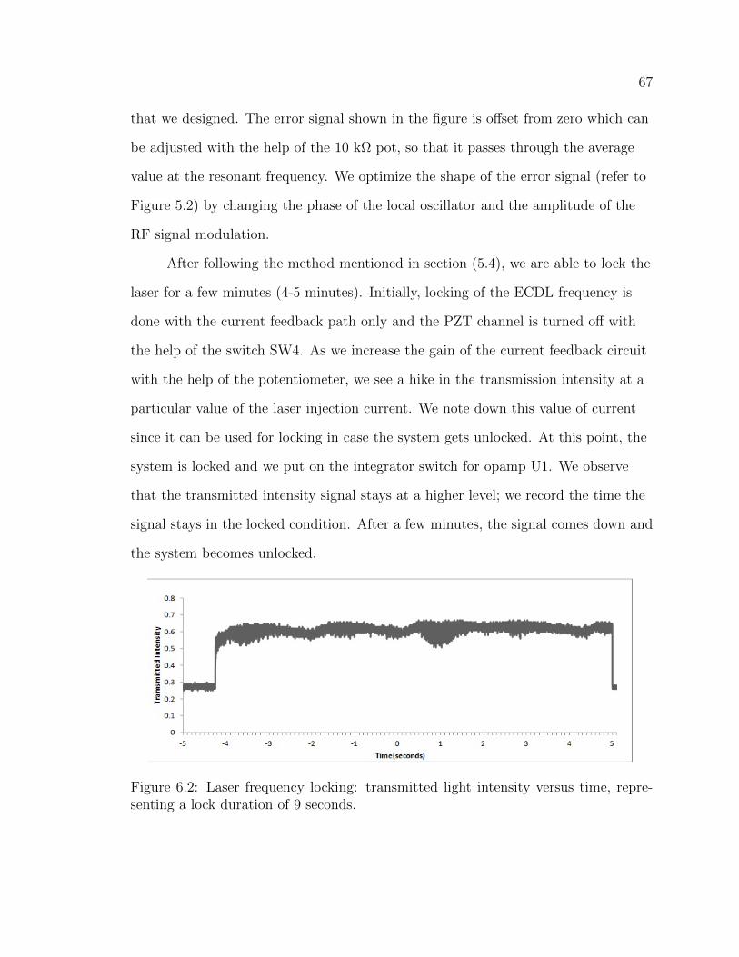
67
that we designed. The error signal shown in the figure is offset from zero which can
be adjusted with the help of the 10 kΩ pot, so that it passes through the average
value at the resonant frequency. We optimize the shape of the error signal (refer to
Figure 5.2) by changing the phase of the local oscillator and the amplitude of the
RF signal modulation.
After following the method mentioned in section (5.4), we are able to lock the
laser for a few minutes (4-5 minutes). Initially, locking of the ECDL frequency is
done with the current feedback path only and the PZT channel is turned off with
the help of the switch SW4. As we increase the gain of the current feedback circuit
with the help of the potentiometer, we see a hike in the transmission intensity at a
particular value of the laser injection current. We note down this value of current
since it can be used for locking in case the system gets unlocked. At this point, the
system is locked and we put on the integrator switch for opamp U1. We observe
that the transmitted intensity signal stays at a higher level; we record the time the
signal stays in the locked condition. After a few minutes, the signal comes down and
the system becomes unlocked.
Figure 6.2: Laser frequency locking: transmitted light intensity versus time, repre-senting a lock duration of 9 seconds.

68
Figure 6.2 displays the plot of the intensity versus time that we obatined while
tuning the frequency of the laser with the current path. We can further increase the
frequency locking time of an ECDL by turning on the switch of the PZT path. We
observe that the polarity of the PZT channel is negative, so we have to use the
optional inverter in our feedback circuit of the PZT (switch SW8 has to be closed).
6.2 Concluding Remarks and Future Work
The purpose of this thesis was to develop an extended cavity diode laser that
is frequency locked to an atomic transition, at a significantly reduced cost compared
to commercially available solutions. We have been successful in characterizing the
various frequency parameters (injection current, temperature, and grating feedback)
and are able to tune the frequency of the diode laser without the use of expensive
electronic devices and circuitry. The cost of a typical commercially available ECDL
system is around 10K USD [25], whereas the overall cost of our device is
approximately 500 USD. This device can be used in undergraduate and graduate
level optics laboratories. We have also designed and built another mount with some
modifications to simplify the control system. This new mount was built to reduce
mode-hopping and efficiently stabilize the temperature of an ECDL. It satisfies the
conditions mentioned in section (2.6) of optimal rotation point to achieve mode-hop
suppression. Figure 6.3 displays the set up of our new mount. This new mount has
been made from scratch with all the components built in our mechanical workshop.
In the future, we can develop a number of these mounts, as well as locking circuits,
that can an be a useful light source for spectroscopy experiments in our research,
laboratory, and courses.
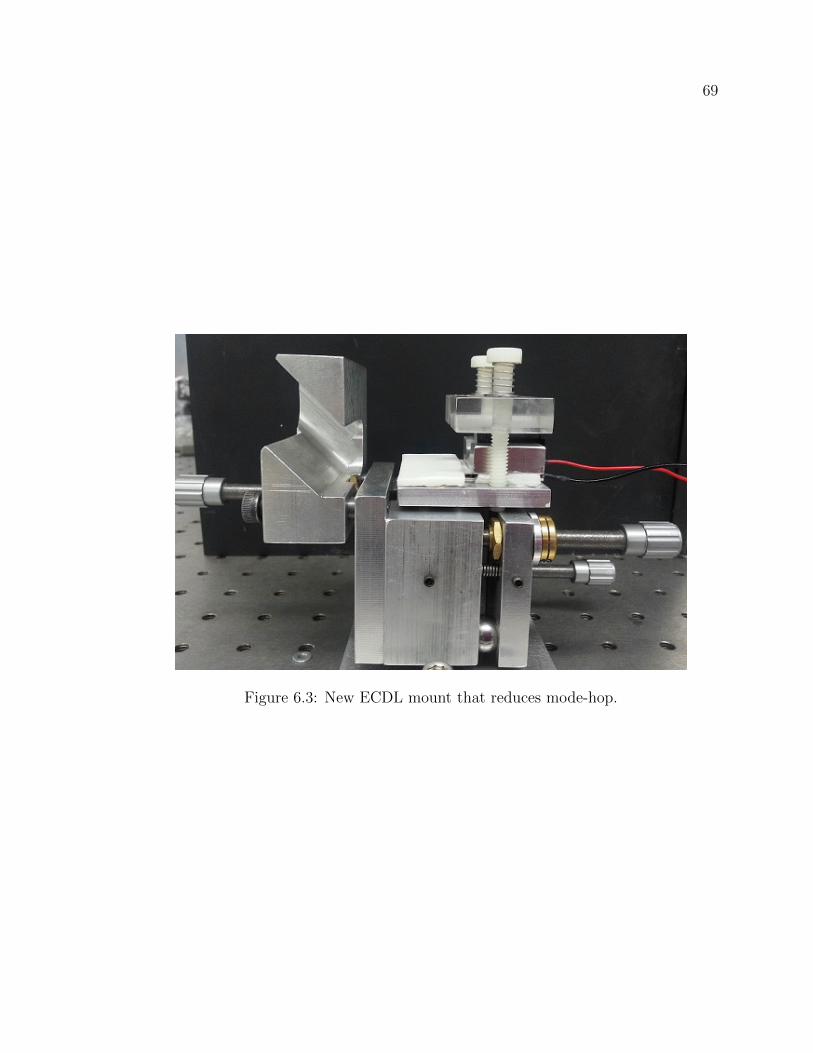
69
Figure 6.3: New ECDL mount that reduces mode-hop.
70
BIBLIOGRAPHY
[1] C. Ye, Tunable External Cavity Diode Lasers. World Scientific, 2004.
[2] M. Schu, External Cavity Diode Lasers: Controlling Laser Output Via OpticalFeedback. College of William and Mary, 2003.
[3] W. T. Silfvest, Fundamentals of Photonics-LASERS, 2005.
[4] B. Saleh and M. Teich, Fundamentals of Photonics. Wiley Series in Pure andApplied Optics, Wiley, 2007.
[5] N. Corporation, “Laser Diode Technology,” 2013. [Online; accessed Jan-2014].
[6] I. Poole, “Laser diode types-radio electronics.”http://www.radio-electronics.com/info/data/semicond/laser_diode/
types-laser-diodes.php, 2013. [Online; accessed Nov-2013].
[7] J. Crowe and R. Craig Appl. Phys. Lett., vol. 5, p. 72, 1964.
[8] C. E. Wieman and L. Hollberg, “Using diode lasers for atomic physics,” Reviewof Scientific Instruments, vol. 62, pp. 1–20, Jan. 1991.
[9] P. Zorabedian, “Tunable external-cavity semiconductor lasers,” in F. J. Duarte(ed.), Tunable Lasers, p. 349, 1995.
[10] A. S. Arnold, J. S. Wilson, and M. G. Boshier, “A simple extended-cavity diodelaser,” Review of Scientific Instruments, vol. 69, pp. 1236–1239, Mar. 1998.
[11] C. A. Heredia, “Diode laser with external grating based cavity,” tech. rep., SanLuis Obispo, California, 2004.
[12] B. Azmoun and S. Metz, “Recipe for locking an extended cavity diode laserfrom the ground up,” tech. rep., Stony Brook University, New york, 2000.
[13] S. L. Cornish, “Introduction to Diode Lasers.”http://massey.dur.ac.uk/resources/grad_skills/LaserExpts.pdf, 2007.[Online; accessed Aug-2013].
[14] M. de Labachelerie and G. Passedat, “Mode-hop suppression of littrowgrating-tuned lasers,” Appl. Opt., vol. 32, pp. 269–274, Jan 1993.
71
[15] H. Tabuchi and H. Ishikawa, “External grating tunable mqw laser with widetuning range of 240 nm,” Electronics Letters, vol. 26(3), pp. 742–743, May 1990.
[16] F. Favre, “External-cavity semiconductor laser with 15 nm continuous tuningrange,” Electronics Letters, vol. 22(3), pp. 795–796, Jul 1986.
[17] L. Levin, “Mode-hop-free electro-optically tuned diode laser,” Optics Letters,vol. 27(4), pp. 237–239, Feb 2002.
[18] M. Juarez and P. Oxley, “The Use of a Lock-In Amplifier to Stabilize theFrequency of a Diode Laser,” Master’s thesis, College of the HolyCross-Massachusetts, 2009.
[19] D. University-UK, “Doppler-Free Saturated Absorption Spectroscopy-LaserSpectroscopy.” [Online; accessed Sep-2013].
[20] D. of Physics-University of Florida, “Saturated Absorption Spectroscopy.”http://www.phys.ufl.edu/courses/phy4803L/group_III/sat_absorbtion/
SatAbs.pdf, 2010. [Online; accessed Sep-2013].
[21] C. University-California, “Ph 77 Advanced Physics Laboratory-Atomic andOptical Physics-Diode Laser Characteristics.”http://www.its.caltech.edu/~ph76a/satabs.pdf. [Online; accessedJul-2013].
[22] R. W. Fox, C. W. Oates, and L. W. Hollberg, “1. stabilizing diode lasers tohigh-finesse cavities,” in Cavity-Enhanced Spectroscopies (R. D. van Zee andJ. P. Looney, eds.), vol. 40 of Experimental Methods in the Physical Sciences,pp. 1 – 46, Academic Press, 2003.
[23] M. C. R. Hoogeveen, “Stabilizing a diode laser to an external reference,”Master’s thesis, KVI-Kernfysisch Versneller Instituut, 2003.
[24] I. DesignSoft, “TINA-V10,” 2012. [Online; accessed Jul-2013].
[25] I. Thorlabs, “Thorproducts.”http://www.thorlabs.us/thorproduct.cfm?partnumber=TLK-L780M.[Online; accessed Mar 6-2014].

72
APPENDIX A
PRINTED CIRCUIT BOARD
This section describes in some detail, the printed circuit board (PCB) of our
locking circuit. We design the schematic of the circuit in Eagle cadsoft free student
version that allows us to generate a board layout of 4 inches by 3 inches. Our PCB
is a double sided board with ground plane as the bottom layer. Figure A.1 shows
Figure A.1: PCB Board (a) front panel and (b) back panel.
the front and back panel of our PCB, whereas Figure A.2 displays the board layout
with traces in blue and red. The blue traces show the connections at the bottom
layer. There are six circular mounting pads (3mm diameter) for the external
connections such as + supply, - supply, V(laser diode current), V(PZT),
V(Photodiode signal input) and RF oscillator output. The square mounting pad is
for connecting the circuit ground with the external ground. The locking circuit
consists of two parts, the error signal circuit and the feedback loop filter circuit.

73
The error signal circuit includes components like an RF oscillator, a phase shifter, a
frequency mixer and a low pass filter. A surface mount voltage controlled oscillator
(minicircuit model-JTOS-25+) is used to generate signals of frequency 15 MHz.
The maximum tuning voltage for this oscillator is +12 V, so we connect a 10 kΩ pot
Figure A.2: Board layout with traces.
across the tuning voltage pin of the oscillator and adjust it to set the oscillator
frequency to its nominal value of 15 MHz. The phase shifter in the circuit is a
minicircuit SPH-16+ ( 50 Ω, 180o voltage variable) and operates at 13-16 MHz
frequency range. A surface mount minicircuit (ADE-1+) frequency mixer of level 7
(LO power+7 dBm) is used to produce new signals at the sum (f1 + f2) and
difference (f1 - f2) of the original frequencies f1 and f2. A low pass filter (minicircuit
model-SCLF-8+) that has a pass band above the unity gain frequency of the
feedback circuit but below the modulation frequency is used to filter the error
signal. The circular mounting pad on the upper left corner provides the RF signal
for frequency modulation, i.e., we connect an external wire from the pad to the laser

74
diode current injection terminal via a bias tee.
The feedback loop filter circuit is designed using the schematic shown in
Figure 5.4. The low pass filtered version of the error signal goes to the feedback
amplifier circuit containing an opamp 355, which is a surface mount and has a
SO-23-6- package PCB layout. The amplified signal from this opamp splits into two
channels. One channel goes to another opamp 355 for further gain in the signal and
the output of which goes to mounting pad V(laser diode current) for tuning the
frequency through current injection. The other channel goes to opamp LM741
which is a through hole device and has a 8-DIP package attached to an 8 pin socket.
The output of the signal from this channel goes to the mounting pad V(PZT).
There are five potentiometers in the circuit. 10 kΩ pots are used to change the
phase of the signal at the phase shifter and set the DC offset of the error signal.
Another 20 kΩ pot is used to set the DC offset of the operational amplifiers. To
increase the gain of the signal in the current path, a pot of 2.5 kΩ is used in the
circuit. The potentiometers are soldered through hole devices with 5 pins, out of
which 2 pins are soldered for mechanical support. Two voltage regulators (digikey
part-MIC5270-3.0YM5 TR) of SOT-753 package and (digikey
partl-ZLDO1117G25TA) SOT-223-3 package are used to provide -3 V and +2.5 V
supply to the OPA 355, whereas the +15 V and -15 V supply is provided to the LM
741 opamps. All the resistors used in the circuit are through hole devices while the
capacitors are surface mounts of case style C1206. Six toggle switches are used in
the circuit to control the various functions and operations of the circuit. We also
add 4 large mounting holes in the corners of the board to mechanically mount the
board (with screws).