characterization of the electrical contact between a ...characterization of the electrical contact...
TRANSCRIPT
Characterization of the electrical contact between a conductive atomic forcemicroscope cantilever and a carbon nanotube
Tarek K. Ghanem, Ellen D. Williams, and Michael S. Fuhrera)
Department of Physics and Center for Nanophysics and Advanced Materials, University of Maryland,College Park, Maryland 20742-4111, USA
(Received 11 April 2011; accepted 21 July 2011; published online 1 September 2011)
A full characterization of the electrical contact between conductive atomic force microscope
(AFM) cantilevers and carbon nanotubes (CNTs) is presented. The dependence of current through
the contact on loading force, geometric parameters, bias conditions, and time is studied in a
two-terminal configuration, where a gold coated AFM cantilever serves as a movable electrode.
We find that for an optimized placement of the cantilever relative to the CNT, the current through
the contact becomes independent of the loading force beyond a certain limit, and this behavior is
also independent of bias conditions. In that load-independent regime, the contact is stable in time
to within the current fluctuations imposed by 1/f and telegraph noise in the CNT channel. Under
certain conditions of tip placement, the current through the contact exhibits a non-monotonic
behavior with loading, which is well explained by the parasitic planar motion of the cantilever.VC 2011 American Institute of Physics. [doi:10.1063/1.3626811]
I. INTRODUCTION
Employing a conductive AFM cantilever as a movable
electrode to perform electrical transport measurements in car-
bon nanotubes (CNTs) is a technique that has been frequently
reported in literature.1–6 The main reason for using this tech-
nique is to measure transport properties as a function of chan-
nel length, thus separating contact effects3,7 from the intrinsic
response of the CNT channel, which is important for under-
standing scattering mechanisms,4,7 and possibly other trans-
port phenomena such as localization.2,6 Despite the large
volume of work using this technique, only a few attempts at
characterization have been made,1,8,9 where the obtained
responses were analyzed in terms of band structure modula-
tion caused by the radial deformation of the CNT,10–14 which
is induced by the tip at the contact point.
For the movable electrode technique, the contact resist-
ance between the CNT and the metal coated AFM cantilever
will change every time the contact is established, which
causes an undesirable scatter in length-dependent transport
data. This problem can usually be circumnavigated by using
a three-terminal technique.3,4 However, it is still important
to understand how to obtain these temporary contacts in a
controlled and reproducible manner, and the variables which
affect them.
In the current work, a full characterization of the electri-
cal contact between conductive AFM cantilevers and CNTs
is presented. We employ a two-terminal configuration, as is
shown in Fig. 1, where the CNT channel is defined between
a fixed electrode and a point that is contacted by the conduc-
tive AFM cantilever. The conductive cantilever also provides
the drain voltage, Vd, while the backgate provides the gate
voltage, Vg. Measurements were performed on seven differ-
ent CNTs whose properties are summarized in Table I. Our
measurements indicate that an important factor is the para-
sitic planar motion acquired by the AFM tip during loading,
which can cause diverse current versus loading behavior.
The measurements also indicate that a properly positioned
cantilever forms a stable reproducible contact with the CNT
where the contact resistance is independent of the loading
force beyond a certain limit, and that this behavior is largely
independent of the bias conditions.
II. EXPERIMENTAL SETUP
We used chemical vapor deposition (CVD) to grow
CNTs according to published recipes.15,16 The substrate used
is heavily doped Si which has a 500 nm oxide layer and also
serves as a backgate. After CVD, we thermally evaporated a
single gold electrode (without an adhesion layer) which is
defined by a shadow mask. Gold has been reported before to
form ohmic contacts to CNTs.2,3 After the gold evaporation,
the sample is fixed to a suitable holder, wire bonded, and in-
stalled in an AFM (model Dimension 5000 from Veeco
Instruments) which is also equipped with a closed loop
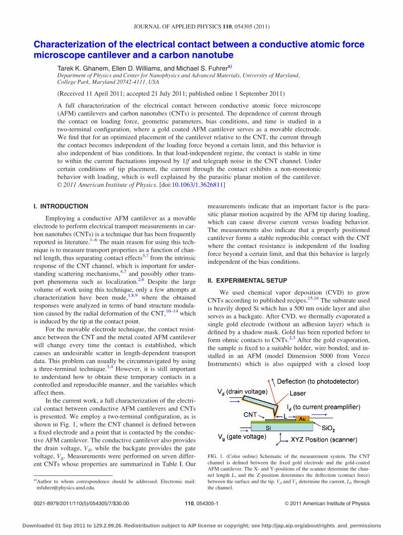
FIG. 1. (Color online) Schematic of the measurement system. The CNT
channel is defined between the fixed gold electrode and the gold-coated
AFM cantilever. The X- and Y-positions of the scanner determine the chan-
nel length L, and the Z-position determines the deflection (contact force)
between the surface and the tip. Vd and Vg determine the current, Id, through
the channel.
a)Author to whom correspondence should be addressed. Electronic mail:
0021-8979/2011/110(5)/054305/7/$30.00 VC 2011 American Institute of Physics110, 054305-1
JOURNAL OF APPLIED PHYSICS 110, 054305 (2011)
Downloaded 01 Sep 2011 to 129.2.99.26. Redistribution subject to AIP license or copyright; see http://jap.aip.org/about/rights_and_permissions
scanner (model NPXYZ100B from nPoint, Inc.). We used
two different types of AFM cantilevers in our measurements,
FESP (k¼ 2.8 N/m) and LTESP (k¼ 48 N/m), both from
Veeco Instruments. We will refer to these as ‘soft cantile-
vers,’ and ‘hard cantilevers,’ respectively. To make them
conductive, we coated the raw Si cantilevers with a 50–60
nm layer of titanium followed by 60–90 nm of gold using
thermal evaporation. The outer gold coating is what contacts
the CNTs.
The measurement procedure begins by searching, via
conventional intermittent-contact AFM imaging, for a CNT
that is contacted by the fixed gold electrode at one end. Then
the AFM scanning motion and the AC vibrations of the can-
tilever are stopped. The cantilever is positioned and brought
down to the surface such that it contacts the CNT somewhere
between its free end and the fixed electrode.
The formation of a cantilever-CNT contact can be
expected to have both electronic and mechanical aspects,
and therefore, it depends on the parameters of both the CNT
and the cantilever. The parameters related to the metal
coated AFM cantilever are its force constant, its dimensions,
and the coating metal, which, in the case of semiconducting
CNTs, determines whether the electrical contact is of the
Ohmic or Schottky barrier type.17,18 The relevant parameters
for the CNT are its type, i.e., whether it is metallic or semi-
conducting, its diameter (which determines the bandgap for
a semiconducting CNT), and its geometric orientation rela-
tive to the cantilever. We also studied the dependence of
the contact on the lateral position (i.e., the position along the
direction normal to the CNT axis) of the tip relative to the
CNT. We will discuss the dependence of the contact on these
parameters in the next sections.
III. RESULTS AND DISCUSSION
A. Conductance versus load behavior
To investigate the behavior of the contact as a function
of loading force, points along the CNTs were selected as
described in Sec. II. At each of these positions, we per-
formed a number of loading cycles where the cantilever is
lowered in successive steps of dZ¼ 2.5 nm, and we simulta-
neously recorded the Z-displacement of the scanner, deflec-
tion of the cantilever, and current passing through the CNT
device after each step, until a specified deflection setpoint
was reached. Then the same procedure was repeated with the
cantilever moving up, until the mechanical contact with the
surface was lost. We will refer to these measurements
throughout as “current-loading curves,” where “loading”
here means either loading or unloading.
At each point along the CNT, we changed the lateral
position (perpendicular to the CNT axis) of the cantilever by
a few nanometers, and repeated the measurement at each lat-
eral position. The purpose was to investigate whether there is
an optimal combination of loading force and lateral position
that would minimize the contact resistance between the can-
tilever and the CNT. One extreme of the measurement geom-
etry is when the CNT orientation is perpendicular to the long
axis of the cantilever, and therefore the lateral position is
adjusted in the X-direction, as shown in Fig. 2(a). We will
henceforth term this geometry a “perpendicular profile.” In
this geometry, we observed three distinct types of behavior
for current-loading curves. These types are shown in
Figs. 2(b) through 2(d). The cantilever deflection for these
loading cycles is also shown in Fig. 2(e).
For current-loading curves of Type-I represented by
Fig. 2(b), conduction through the CNT device starts simulta-
neously with the mechanical contact (which we define as
Z¼ 0), and the current rises quickly with more loading,
FIG. 2. (Color online) (a) Illustration of the “perpendicular profile” mea-
surement geometry, scan size is 10� 10 lm (cantilever is not drawn to
scale). The edge of the fixed gold electrode can be seen on top. (b)-(d) Cur-
rent-loading curves of Types-I, II, and III, respectively, Z¼ 0 is defined at
the onset of mechanical contact. (e) Deflection corresponding to the three
loading cycles, used to define Z¼ 0. Data in (b) through (d) are taken at the
same point on CNT D7, 19.0 lm away from the fixed gold electrode with
different lateral positions about 25 nm apart (along the X-axis), Vd¼ 0.1 V,
Vg¼� 3.0 V, and Imax¼ 0.21 lA. The cantilever used is a soft cantilever.
TABLE I. Designation, type (semiconducting or metallic), and diameter dof the CNTs studied.
CNT Type d (nm)
D1 semiconducting 2.1
D2 metallic 2.2
D3 semiconducting 3.0
D4 metallic 4.1
D5 semiconducting 1.9
D6 metallic 4.0
D7 metallic 2.0
054305-2 Ghanem, Williams, and Fuhrer J. Appl. Phys. 110, 054305 (2011)
Downloaded 01 Sep 2011 to 129.2.99.26. Redistribution subject to AIP license or copyright; see http://jap.aip.org/about/rights_and_permissions
finally reaching a load-independent value. In current-loading
curves of Type-II, represented by Fig. 2(c), the contact starts
similar to Type-I, but the current rises and then goes back to
zero with more loading, and the current may or may not
reach its maximum possible value in the middle. In current-
loading curves of Type-III, represented by Fig. 2(d), electri-
cal conduction is delayed beyond the mechanical contact,
and then starts to behave similarly to Type-I with more load-
ing. Unloading generally shows similar behavior to loading,
with hysteresis caused by adhesion. Responses which are
somewhat similar to current-loading curves of Type-I and
Type-II have been reported before in the literature.1,8,9 We
have observed these three types of behavior for all of the
CNTs we studied, whether metallic or semiconducting. This
behavior was largely independent of the cantilever force con-
stant and contact type (we obtained Schottky barrier contacts
using a tip covered only with Ti). The behavior observed
exclusively depended on the lateral position of the cantilever
relative to the CNT.
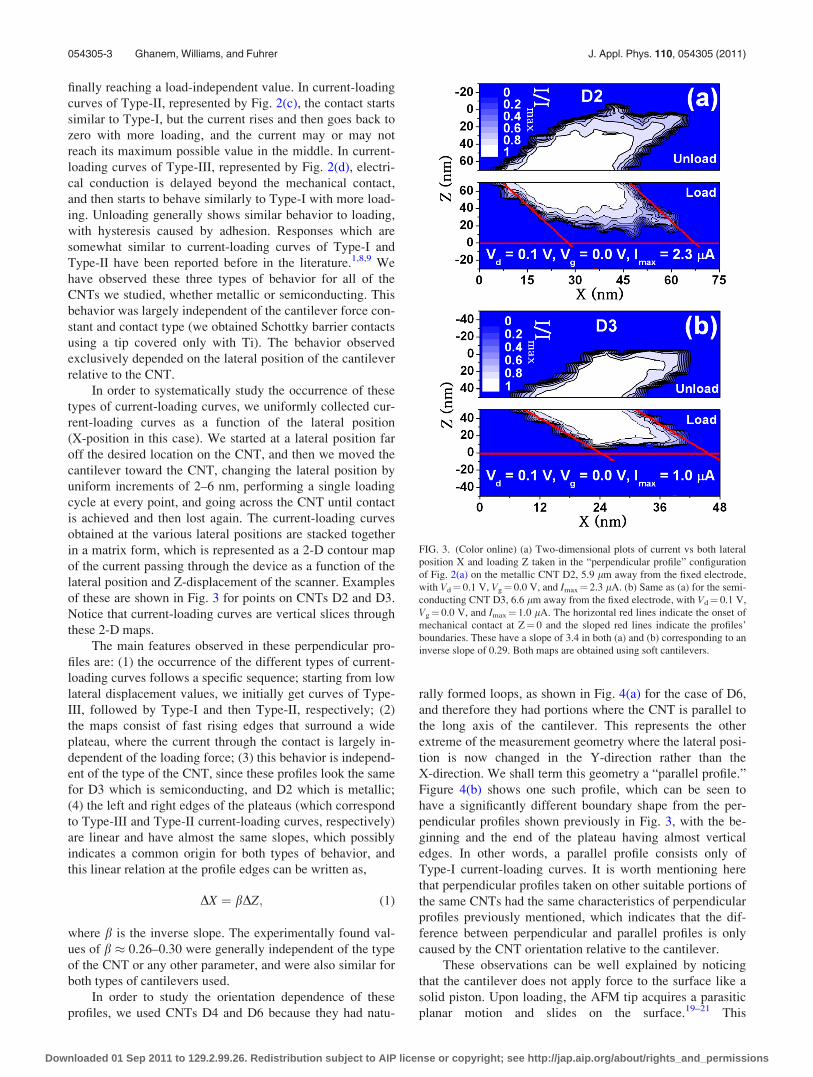
In order to systematically study the occurrence of these
types of current-loading curves, we uniformly collected cur-
rent-loading curves as a function of the lateral position
(X-position in this case). We started at a lateral position far
off the desired location on the CNT, and then we moved the
cantilever toward the CNT, changing the lateral position by
uniform increments of 2–6 nm, performing a single loading
cycle at every point, and going across the CNT until contact
is achieved and then lost again. The current-loading curves
obtained at the various lateral positions are stacked together
in a matrix form, which is represented as a 2-D contour map
of the current passing through the device as a function of the
lateral position and Z-displacement of the scanner. Examples
of these are shown in Fig. 3 for points on CNTs D2 and D3.
Notice that current-loading curves are vertical slices through
these 2-D maps.
The main features observed in these perpendicular pro-
files are: (1) the occurrence of the different types of current-
loading curves follows a specific sequence; starting from low
lateral displacement values, we initially get curves of Type-
III, followed by Type-I and then Type-II, respectively; (2)
the maps consist of fast rising edges that surround a wide
plateau, where the current through the contact is largely in-
dependent of the loading force; (3) this behavior is independ-
ent of the type of the CNT, since these profiles look the same
for D3 which is semiconducting, and D2 which is metallic;
(4) the left and right edges of the plateaus (which correspond
to Type-III and Type-II current-loading curves, respectively)
are linear and have almost the same slopes, which possibly
indicates a common origin for both types of behavior, and
this linear relation at the profile edges can be written as,
DX ¼ bDZ; (1)
where b is the inverse slope. The experimentally found val-
ues of b � 0.26–0.30 were generally independent of the type
of the CNT or any other parameter, and were also similar for
both types of cantilevers used.
In order to study the orientation dependence of these
profiles, we used CNTs D4 and D6 because they had natu-
rally formed loops, as shown in Fig. 4(a) for the case of D6,
and therefore they had portions where the CNT is parallel to
the long axis of the cantilever. This represents the other
extreme of the measurement geometry where the lateral posi-
tion is now changed in the Y-direction rather than the
X-direction. We shall term this geometry a “parallel profile.”
Figure 4(b) shows one such profile, which can be seen to
have a significantly different boundary shape from the per-
pendicular profiles shown previously in Fig. 3, with the be-
ginning and the end of the plateau having almost vertical
edges. In other words, a parallel profile consists only of
Type-I current-loading curves. It is worth mentioning here
that perpendicular profiles taken on other suitable portions of
the same CNTs had the same characteristics of perpendicular
profiles previously mentioned, which indicates that the dif-
ference between perpendicular and parallel profiles is only
caused by the CNT orientation relative to the cantilever.
These observations can be well explained by noticing
that the cantilever does not apply force to the surface like a
solid piston. Upon loading, the AFM tip acquires a parasitic
planar motion and slides on the surface.19–21 This
FIG. 3. (Color online) (a) Two-dimensional plots of current vs both lateral
position X and loading Z taken in the “perpendicular profile” configuration
of Fig. 2(a) on the metallic CNT D2, 5.9 lm away from the fixed electrode,
with Vd¼ 0.1 V, Vg¼ 0.0 V, and Imax¼ 2.3 lA. (b) Same as (a) for the semi-
conducting CNT D3, 6.6 lm away from the fixed electrode, with Vd¼ 0.1 V,
Vg¼ 0.0 V, and Imax¼ 1.0 lA. The horizontal red lines indicate the onset of
mechanical contact at Z¼ 0 and the sloped red lines indicate the profiles’
boundaries. These have a slope of 3.4 in both (a) and (b) corresponding to an
inverse slope of 0.29. Both maps are obtained using soft cantilevers.
054305-3 Ghanem, Williams, and Fuhrer J. Appl. Phys. 110, 054305 (2011)
Downloaded 01 Sep 2011 to 129.2.99.26. Redistribution subject to AIP license or copyright; see http://jap.aip.org/about/rights_and_permissions

mechanical motion can explain the observed behaviors
through the tip sliding away, or toward, the CNT. Following
Huang et al.,20 the relation between the Z-displacement of
the cantilever and the parasitic planar displacement (this dis-
placement is along the long axis of the cantilever, which is
always the X-direction in our setup) is provided by,
DX ¼ tan hþ 3ht=2Lcð ÞDZ; (2)
where h is the cantilever mounting angle, ht is the height of
the tip, and Lc is the length of the cantilever. In our setup
h¼ 12�, and both types of cantilevers used have the typical
values Lc¼ 225 lm and ht¼ 12 lm. Using these values, the
term between the brackets in Eq. (2) which represents the
inverse slope b in Eq. (1) can be found to be 0.29, which is
in good agreement with the experimentally found values of b� 0.26–0.3 for both types of cantilevers.
Now the current versus loading behavior of both profile
types can be qualitatively explained. In the perpendicular
profile configuration, Type-III current-loading curves are
produced by the tip landing too far from the CNT, and as
loading increases, it slides and contacts the CNT. Type-II
can be explained as the tip initially landing on the CNT and
as loading increases, the tip slides off the CNT and electrical
contact is lost. Finally for Type-I, the tip initially lands on
the CNT, however the parasitic planar motion corresponding
to the designated deflection setpoint is not enough to break
the contact before the deflection setpoint is reached. For the
parallel profile geometry, the cantilever slides along the axis
of the CNT, therefore the contact is never lost with more
loading and Type-I behavior is always obtained. These situa-
tions are schematically shown in Fig. 5.
It must be emphasized here that all the diverse switching
behavior reported above is of a purely mechanical origin,
and this should be taken into account before invoking any
interpretation of current versus loading behavior in terms of
material properties at the contact. This also might offer a
simpler explanation for some of the non-monotonic current-
loading behaviors reported in the literature for CNTs.8,9
B. Dependence on bias conditions
We have observed Type-I current-loading curves in all
of the loading experiments we performed on both metallic
and semiconducting CNTs, and we conclude that they are
always obtainable with the proper adjustment of the lateral
position of the cantilever. Furthermore, the current through
the CNTs in the load-independent regime was highly repro-
ducible upon breaking and remaking of the contact several
times, indicating no permanent change of the CNT at the
contact point. We therefore assume that Type-I current-load-
ing curves approximate the true loading behavior of the con-
tact. This is extremely useful when performing local
transport measurements because it means that finding the
minimum contact resistance, (Rc)min, is only a matter of
using the correct deflection setpoint such that the current is
in the load-independent regime, and finding the optimal lat-
eral position where the maximum current is achieved. Now
the local transport problem of measuring R(Vd,Vg,L,Rc),
where Rc varies randomly with L, can be effectively reduced
FIG. 4. (Color online) (a) Illustration of the “parallel profile” measurement
geometry, scan size is 10� 10 lm (cantilever not drawn to scale). (b) Two-
dimensional plot of current vs both lateral position Y and loading Z taken in
the parallel profile configuration shown in (a), the vertical boundaries indi-
cate the presence of only Type-I current-loading curves. The point where the
profile was taken is illustrated in (a), 4.8 lm from the loop junction, which
is 17.8 lm away from the fixed electrode. Vd¼ 0.1 V, Vg¼ 0.0 V, and
Imax¼ 0.7 lA. The map is obtained using a hard cantilever.
FIG. 5. (Color online) Explanation of current-loading curves. (1) Cantilever
approaching the surface, no current flow. (2) Cantilever snaps into mechani-
cal contact with the surface, with onset of current flow, except for Type-III
where the cantilever lands far to the left. (3) Cantilever slides on the surface
with loading, still maintaining contact with the CNT, or initiating contact for
the case of Type-III. (4) The cantilever keeps on sliding with more loading
and contact is maintained, except for Type-II where the cantilever initially
landed far to the right.
054305-4 Ghanem, Williams, and Fuhrer J. Appl. Phys. 110, 054305 (2011)
Downloaded 01 Sep 2011 to 129.2.99.26. Redistribution subject to AIP license or copyright; see http://jap.aip.org/about/rights_and_permissions
into R(Vd,Vg,L), with Rc now being a constant equal to
(Rc)min.
We have also verified that Type-I behavior is independent
of the bias conditions, Vd and Vg. In order to check that, we first
adjust the lateral position such that Type-I current-loading
curves are obtained, then we start a loading cycle where,
instead of measuring a single current point at constant bias con-
ditions for each increment of the Z-displacement, we sweep ei-
ther Vd or Vg while keeping the other voltage constant.
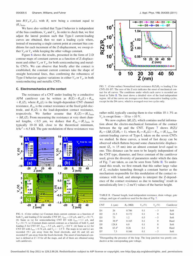
Figure 6 shows the results, presented in the form of 2-D
contour maps of constant current as a function of Z-displace-
ment and either Vd or Vg, for both semiconducting and metal-
lic CNTs. We can observe that briefly after the contact is
established, the constant current contours take the shape of
straight horizontal lines, thus confirming the robustness of
Type-I behavior against variations in either Vd or Vg, in both
semiconducting and metallic CNTs.
C. Electromechanics at the contact
The resistance of a CNT under loading by a conductive
AFM cantilever can be written as R(Z)¼Rnt(L)þRAu
þRc(Z), where Rnt(L) is the length-dependent CNT channel
resistance, RAu is the contact resistance at the fixed gold elec-
trode, and Rc(Z) is the load-dependent contact resistance,
respectively. We further assume that Rc(Z)¼ (Rc)min
þDRc(Z). From measuring the resistance at very short chan-
nel lengths, < 0.5 lm, we deduce that RAuþ (Rc)min is
typically 10-18 kX, close to the theoretical minimum,
h/4e2¼ 6.5 kX. The gate modulation of these resistances was
rather mild, typically causing them to rise within 10 6 3% as
Vg is swept from � 10 to þ10 V.
We now explore DRc(Z), which contains useful informa-
tion about the electro-mechanical formation of the contact
between the tip and the CNT. Figure 7 shows R(Z)/
R0¼ (DRc(Z)/R0þ 1), where R0¼Rnt(L)þRAuþ (Rc)min, for
current-loading curves of Type-I, taken on the seven CNTs
we studied. In these curves, a trend of fast decay can be
observed which flattens beyond some characteristic displace-
ment (Zc � 15 nm) into an almost constant level equal to
one. This distance can be seen to be largely independent of
the CNT type, diameter, and force constant of the cantilever
used, given the diversity of parameters under which the data
of Fig. 7 are taken, as can be seen from Table II. To under-
stand this result, we first remark that this rather large value
of Zc excludes tunneling through a constant barrier as the
mechanism responsible for this modulation of the contact re-
sistance with load, and attempts to interpret the Z-depend-
ence of the contact resistance as due to tunneling1 result in
unrealistically low (�2 meV) values of the barrier height.
FIG. 6. (Color online) (a) Constant drain current contours as a function of
both Vg and loading Z for metallic CNT D7. Imax¼ 2.8 lA, and Vd¼ 0.1 V.
(b) Same as (a) for semiconducting CNT D3 with Imax¼ 1.1 lA, and
Vd¼ 0.1 V. (c) Constant drain current contours as a function of both Vd and
loading Z for CNT D7. Imax¼ 5.5 lA, and Vg¼ 0.0 V. (d) Same as (c) for
CNT D3 with Imax¼ 0.74 lA, and Vg¼� 2.5 V. The maps in (a) and (c) are
recorded 19.1 lm away from the fixed electrode, and (b) and (d) are
recorded 87 lm away from the fixed electrode. The onset of mechanical con-
tact is defined at Z¼ 0 for all the maps, and all of them are obtained using
soft cantilevers.
FIG. 7. (Color online) Normalized total resistance R(Z)/R0 vs loading Z for
CNTs D1-D7. The zero of the Z-axis indicates the onset of mechanical con-
tact for all curves. The conditions under which each curve is recorded are
listed in Table II. The inset shows a detailed view of the load-independent
region. All of the curves are averages over three consecutive loading cycles,
except for the D4 curve, which is averaged over two cycles only.
TABLE II. Channel length, load-independent resistance, drain voltage, gate
voltage, and type of cantilever used for the data of Fig. 7.
CNT L (lm) R0 (MX) Vd (V) Vg (V) Cantilever
D1 26 0.786 0.1 � 3 Soft
D2 21.5 0.172 0.1 0 Soft
D3 73 1.2 0.5 � 5 Soft
D4 38.9a 0.165 0.1 0 Hard
D5 128.8 6.0 0.1 0 Soft
D6 63.4a 0.26 0.1 0 Hard
D7 7.3 0.166 0.1 � 3 Soft
aDisregarding the presence of the loop. The loop junction was poorly con-
ductive at the corresponding gate voltage.
054305-5 Ghanem, Williams, and Fuhrer J. Appl. Phys. 110, 054305 (2011)
Downloaded 01 Sep 2011 to 129.2.99.26. Redistribution subject to AIP license or copyright; see http://jap.aip.org/about/rights_and_permissions
Instead, we interpret the Z-dependence of the contact re-
sistance as due to the modulation of the barrier for carrier
injection from the tip into the CNT by the stress at the con-
tact. This stress-induced modulation of the injection barrier
could be associated with deformation of the gold film at the
tip, with some stress needed to bring a certain number of
gold grains into contact with the CNT.22 Also, some theoreti-
cal calculations predict the presence of a tunnel barrier in the
case of gold contacts to CNTs,23,24 and a dependence of this
barrier on the electrode-CNT separation within atomic-scale
distances,24,25 where this tunnel barrier becomes smaller
with a smaller metal-CNT distance, which establishes a pos-
sible route for the modulation of the contact resistance
through contact stress.
We now discuss whether radial deformation of the
CNT induced by the tip at the contact point could have
played a role in our measurements. The similar behavior
of contacts to both metallic and semiconducting CNTs
exhibited in all our measurements, and the independence
of bias conditions discussed in Sec. III B, seem to contra-
dict some theoretical expectations10–14 which predict that
semiconducting and metallic CNTs respond in a different
way to radial deformation, which could open a gap in me-
tallic CNTs, while narrowing the gap for semiconducting
CNTs.
The previous attempts to understand this problem1,8,9
have employed a Hertz contact model between a sphere repre-
senting the tip and a cylinder representing the CNT, where
the contact force between the tip and the substrate is assumed
to be entirely transmitted across the CNT. We believe this
picture is unrealistic mainly because it ignores the yielding
mechanics of the metallic coating covering the tip. It also
ignores the parasitic planar motion of the tip as it contacts the
surface previously discussed, and the inevitable presence of
asymmetries in cantilever manufacturing and mounting, or
microscopic roughness of the tip or substrate. All of these fac-
tors can cause some part of the tip to be in touch with the sub-
strate at the contact point, thus invalidating the assumption
that force is transmitted from the tip to the substrate entirely
across the CNT, which possibly leads to an overestimation of
the mechanical stress at the tip-CNT contact.
In particular, an AFM cantilever coated with a ductile
metal such as gold would acquire a rather flat profile upon
contacting the surface, which suggests that the average stress
around the CNT is mainly determined by the mechanics of
the substrate/tip contact. In this case, the maximum stress
that could be applied by the tip corresponds to the limit of a
fully plastic contact, and would be limited to about 2.2 rY,
where rY is the yield strength of the coating metal.26 For
gold, rY can have a rather wide range, 55–220 MPa, depend-
ing on preparation conditions and sample dimensions.27
Even by considering the upper limit of these values for rY,
the stress around the CNT would still be limited to about 480
MPa. This stress level is significantly lower than the theoreti-
cally expected minimum stress required for radial deforma-
tion to occur,28 estimated to be about 700 MPa for a CNT
having a diameter around 2 nm,28 which is approximately
the case for all the CNTs we studied, except for D4 and D6.
Therefore, radial deformation of these CNTs by a soft metal
such as gold is unlikely. In other words, the more rigid CNT
is more likely to cut through the more ductile gold and not
vice versa. The larger diameter CNTs, D4 and D6 (whose
diameters �4 nm), were probably multiwalled, and therefore
the minimum pressure to cause radial deformation in these is
probably higher than the value of �100 MPa predicted by
Hasegawa et al.28 for a single walled carbon CNT having
that diameter.
The assumption that radial stress on the CNT is limited
through plastic deformation of the gold coating can also
explain the similar values of the characteristic displacement
for obtaining a load-independent contact (Zc� 15 nm)
between soft and hard cantilevers, which apply nominally
different forces at the same displacement due to their differ-
ent spring constants. It is also consistent with our observation
of a large disparity in the tip diameters of soft and hard canti-
levers, which can be seen in the width of the plateau region
through measurements such as Figs. 3(a), 3(b), and 4(b), and
was further confirmed through SEM imaging of the tips after
these contact experiments were performed. We consistently
observe much larger tip diameters for hard cantilevers, sug-
gesting that the larger force for hard cantilevers at a given
displacement is spread out over a larger tip area due to plas-
ticity of the gold coating.
D. Temporal stability of the contact
Temporal stability of the contact is an important opera-
tional aspect for performing local transport measurements,
where the contact needs to be stable for at least the duration
of a typical voltage sweep. The contact becomes destabilized
through the tip sliding off the CNT, which can happen
directly through drift in the X- and Y-directions. Drift in the
Z-direction does not directly alter the contact in the load-in-
dependent regime. However, it still can indirectly destabilize
the contact through parasitic planar motion. Typically, we
found the drift to be about 0.2 nm/min for the X and Y direc-
tions, and about 0.2 nm/s for the Z direction under warm up
conditions, and dropping to less than half these values under
steady state conditions. In order to further characterize the
temporal stability of our system, we first tuned the lateral
position, such as to obtain a current-loading curve of Type-I,
and then simultaneously recorded the deflection of the canti-
lever and the current through the CNT device as a function
of time. This was done in two modes, where in the first
mode we applied feedback such that the deflection is kept
constant, and in the second mode the deflection was left to
freely drift. We found that in our system, the current was
generally stable within a margin of 6 4%, for times of 2–6
min in the first (deflection stabilized) mode, and 1–2 min
without deflection stabilization. The current fluctuations gen-
erally had a 1/f c spectrum where c � 1–1.5, and did not cor-
relate with the deflection fluctuations, which in the
frequency range studied (< 50 Hz), showed mostly a white
spectrum. These observations suggest that the sources of cur-
rent fluctuations in the load-independent regime are the 1/fand telegraph noise in the CNT channel29–31 rather than fluc-
tuations of the contact resistance between the CNT and the
movable electrode.
054305-6 Ghanem, Williams, and Fuhrer J. Appl. Phys. 110, 054305 (2011)
Downloaded 01 Sep 2011 to 129.2.99.26. Redistribution subject to AIP license or copyright; see http://jap.aip.org/about/rights_and_permissions
IV. CONCLUSION
It is possible to establish a good and reproducible electri-
cal contact between a conductive AFM cantilever and a CNT.
For an optimized placement of the tip relative to the CNT, the
contact resistance is independent of the loading force beyond
a certain limit, and this behavior is also independent of the
bias conditions, and thus is equivalent to a temporary fixed
electrode. Under certain conditions of tip placement relative
to the CNT, the current through the contact shows non-mono-
tonic behavior with loading. This behavior results largely
from the parasitic planar motion of the cantilever during load-
ing. We do not observe any clear evidence indicating a change
in the electronic properties of the CNTs caused by loading at
the contact point, and suggest that radial stress is largely lim-
ited by the plastic deformation of the soft coating metal. The
contact is stable in time to within our ability to measure, set
by the current fluctuations imposed by 1/f and telegraph noise
in the CNT channel.
ACKNOWLEDGMENTS
This work has been supported by the University of
Maryland NSF-MRSEC under Grant No. DMR 05-20471.
MRSEC Shared Experimental Facilities were used in this
work.
1P. J. de Pablo, M. T. Martınez, J. Colchero, J. Gomez-Herrero, W. K.
Maser, A. M. Benito, E. Munoz, and A. M. Baro, Adv. Mater. 12, 573
(2000).2P. J. de Pablo, C. Gomez-Navarro, J. Colchero, P. A. Serena, J. Gomez-
Herrero, and A. M. Baro, Phys. Rev. Lett. 88, 036804 (2002).3Y. Yaish, J. Y. Park, S. Rosenblatt, V. Sazonova, M. Brink, and P. L.
McEuen, Phys. Rev. Lett. 92, 046401 (2004).4J. Y. Park, S. Rosenblatt, Y. Yaish, V. Sazonova, H. Ustunel, S. Braig,
T. A. Arias, P. W. Brouwer, and P. L. McEuen, Nano Lett. 4, 517 (2004).5C. Gomez-Navarro, P. J. D. Pablo, J. Gomez-Herrero, B. Biel, F. J. Gar-
cia-Vidal, A. Rubio, and F. Flores, Nature Mater. 4, 534 (2005).
6P. Sundqvist, F. J. Garcia-Vidal, F. Flores, M. Moreno-Moreno, C.
Gomez-Navarro, J. S. Bunch, and J. Gomez-Herrero, Nano Lett. 7, 2568
(2007).7X. Zhou, J.-Y. Park, S. Huang, J. Liu, and P. L. McEuen, Phys. Rev. Lett.
95, 146805 (2005).8C. Gomez-Navarro, P. J de Pablo, and J. Gomez-Herrero, Adv. Mater. 16,
549 (2004).9C. Gomez-Navarro, J. J. Saenz, and J. Gomez-Herrero, Phys. Rev. Lett.
96, 076803 (2006).10C.-J. Park, Y.-H. Kim, and K. J. Chang, Phys. Rev. B 60, 10656 (1999).11C. Kilic, S. Ciraci, O. Gulseren, and T. Yildirim, Phys. Rev. B 62, R16345
(2000).12O. Gulseren, T. Yildirim, S. Ciraci, and C. Kilic, Phys. Rev. B 65, 155410
(2002).13Y. Umeno, T. Kitamura, and A. Kushima, Comput. Mater. Sci. 30, 283
(2004).14H. Mehrez, A. Svizhenko, M. P. Anantram, M. Elstner, and T. Frauen-
heim, Phys. Rev. B 71, 155421 (2005).15Y. Li, W. Kim, Y. Zhang, M. Rolandi, D. Wang, and H. Dai, J. Phys.
Chem. B 105, 11424 (2001).16W. Kim, H. C. Choi, M. Shim, Y. Li, D. Wang, and H. Dai, Nano Lett. 2,
703 (2002).17S. Heinze, J. Tersoff, R. Martel, V. Derycke, J. Appenzeller, and P. Avou-
ris, Phys. Rev. Lett. 89, 106801 (2002).18A. Javey, J. Guo, Q. Wang, M. Lundstrom, and H. Dai, Nature (London)
424, 654 (2003).19J. H. Hoh and A. Engel, Langmuir 9, 3310 (1993).20L. Huang, C. Meyer, and C. Prater, J. Phys.: Conf. Ser. 61, 805 (2007).21R. J. Cannara, M. J. Brukman, and R. W. Carpick, Rev. Sci. Instrum. 76,
053706 (2005).22S.-H. Ke, W. Yang, and H. U. Baranger, J. Chem. Phys. 124, 181102
(2006).23S. Dag, O. Gulseren, S. Ciraci, and T. Yildirim, Appl. Phys. Lett. 83, 3180
(2003).24B. Shan and K. Cho, Phys. Rev. B 70, 233405 (2004).25I. Deretzis and A. L. Magna, Nanotechnology 17, 5063 (2006).26J. Jamari and D. J. Schipper, J. Tribol. 128, 230 (2006).27H. D. Espinosa, B. C. Prorok, and B. Peng, J. Mech. Phys. Solids 52, 667
(2004).28M. Hasegawa and K. Nishidate, Phys. Rev. B 74, 115401 (2006).29P. G. Collins, M. S. Fuhrer, and A. Zettl, Appl. Phys. Lett. 76, 894 (2000).30F. Liu, K. L. Wang, C. Li, and C. Zhou, IEEE Trans. Nanotechnol. 5, 441
(2006).31M. Ishigami, J. H. Chen, E. D. Williams, D. Tobias, Y. F. Chen, and M. S.
Fuhrer, Appl. Phys. Lett. 88, 203116 (2006).
054305-7 Ghanem, Williams, and Fuhrer J. Appl. Phys. 110, 054305 (2011)
Downloaded 01 Sep 2011 to 129.2.99.26. Redistribution subject to AIP license or copyright; see http://jap.aip.org/about/rights_and_permissions