charge-sensitive front end circuitspoc/talks/course2 handouts.pdf · room temperature semiconductor...
TRANSCRIPT

1
Charge-Sensitive Front End Circuits
Paul O’Connor, Brookhaven National Laboratory
IEEE Nuclear Sciences Symposium/Medical Imaging Conference/Workshop on
Room Temperature Semiconductor Detectors
November 5, 2001
2
Outline
• Custom monolithic front ends– advantages– access to technology– design tools
• Low noise analog design in monolithic CMOS– preamplifier design– shaping amplifier
• Circuit examples• CMOS Scaling and Charge Sensitive Amplifier design
– noise mechanisms in scaled devices– optimum capacitive match to detector– noise, dynamic range, and power vs. scaling length

2
3
Outline
• Custom monolithic front ends– advantages– access to technology– design tools
• Low noise analog design in monolithic CMOS– preamplifier design– shaping amplifier
• Circuit examples• MOS Scaling and Charge Sensitive Amplifier design
– noise mechanisms in scaled devices– optimum capacitive match to detector– noise, dynamic range, and power vs. scaling length
4
• Can be efficiently mass-produced with excellent economy of scale:– E.g., maskset + 10 wafers ~ $100K, 1000 chips/wafer– Additional wafer ~ $5K– Incremental cost < $10/chip– Chip may have 16 – 128 channels
• Can be located close to dense detector electrode arrays– pixels, micropattern & segmented cathode designs
• Can combine functions on single chip, replacing PCB/hybrid/cable connections with lower cost on-chip connection
• Can reduce power*
Custom monolithic front ends
3
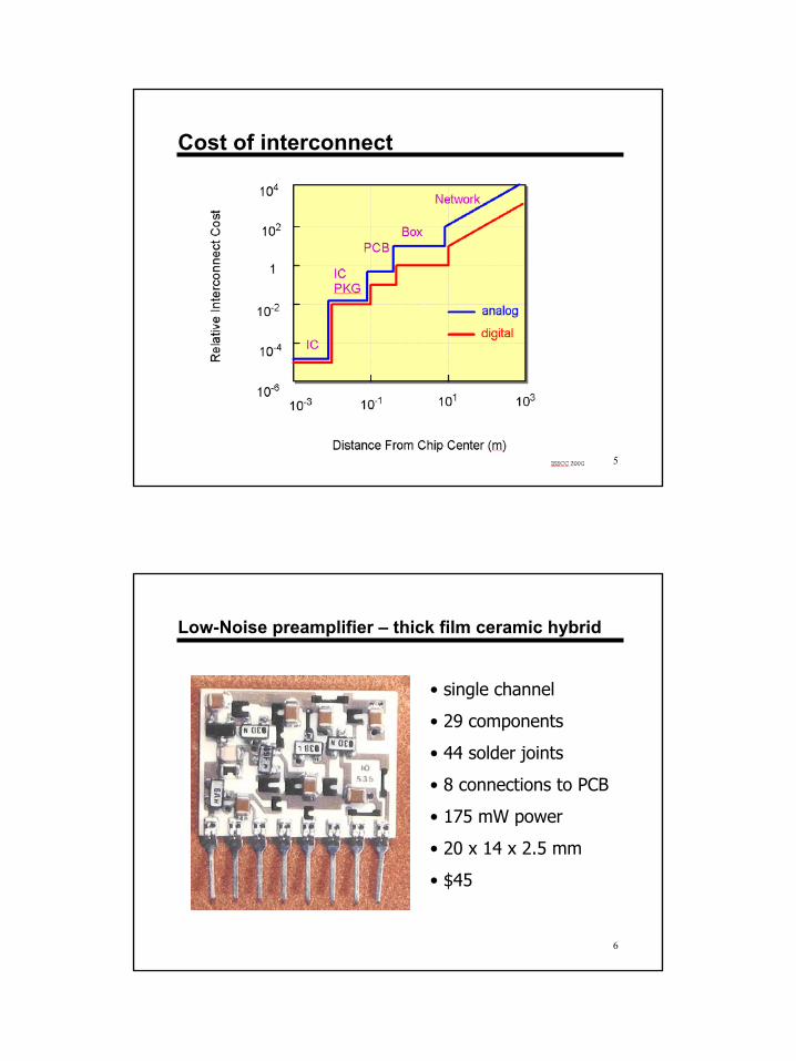
5
Cost of interconnect
6
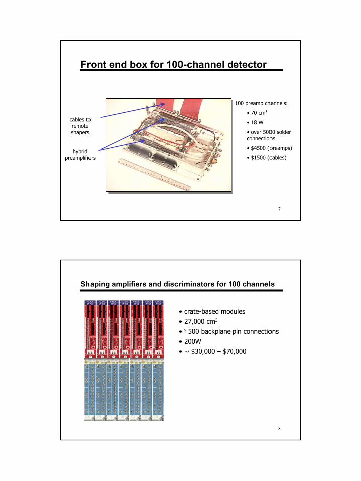
Low-Noise preamplifier – thick film ceramic hybrid
• single channel
• 29 components
• 44 solder joints
• 8 connections to PCB
• 175 mW power
• 20 x 14 x 2.5 mm
• $45
4
7
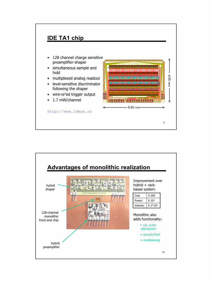
hybrid preamplifiers
100 preamp channels:
• 70 cm3
• 18 W
• over 5000 solder connections
• $4500 (preamps)
• $1500 (cables)
cables to remote shapers
Front end box for 100-channel detector
8
Shaping amplifiers and discriminators for 100 channels
• crate-based modules• 27,000 cm3
• > 500 backplane pin connections• 200W• ~ $30,000 – $70,000
5
9
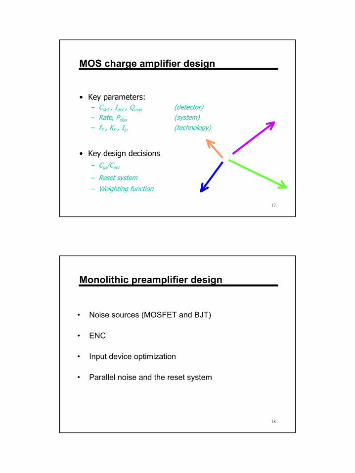
IDE TA1 chip
• 128 channel charge sensitive preamplifier-shaper
• simultaneous sample and hold
• multiplexed analog readout• level-sensitive discriminator
following the shaper• wire-or’ed trigger output• 1.7 mW/channel
http://www.ideas.no
10
Advantages of monolithic realization
hybrid preamplifier
hybrid shaper
128-channel monolithic
front end chip
Improvement over hybrid + rack-based system:
Monolithic also adds functionality:
• cal. pulse distribution
• sample/hold
• multiplexing
X 2*106Volume:
X 103Power:
X 200Cost

6
11
Custom monolithics – technology options
• Bipolar– Workhorse of “old” analog– Available from a handful of
vendors– Speed/power advantage over
CMOS (diminishing)– Low integration density
• Standard CMOS– Suitable for most analog
designs– Best for combining analog and
digital– Highest integration density– Widely available– Short life cycle (3
years/generation)• BiCMOS
– Complex process, expensive
• JFET/CMOS– JFET has low 1/f noise but slow– Unavailable commercially
• Silicon on insulator (SOI)– Modest speed advantage for digital– Drawbacks for analog
• SiGe– Complexity equivalent to BiCMOS– Extremely fast bipolar device plus
submicron CMOS– Availability increasing
• GaAs– Unsuitable for wideband analog
12
Multiproject foundry services
• Combine designs from many institutions on one maskset
• Arrange for regular runs with a variety of popular foundries
• Design support– Models– Design rules– Process monitoring
• Amortize cost of run over many users
In the U.S. Europe
MOSIS service www.mosis.org Europractice www.imec.be/europractice
Custom monolithics: technology access
multiproject wafer

7
13
CMOS layout examples
DigitalAnalog
14

8
15
Outline
• Custom monolithic front ends– advantages– access to technology– design tools
• Low noise analog design in monolithic CMOS– preamplifier design– shaping amplifier
• Circuit examples• CMOS Scaling and Charge Sensitive Amplifier design
– noise mechanisms in scaled devices– optimum capacitive match to detector– noise, dynamic range, and power vs. scaling length
16
Two types of charge sensitive amplifier
1. Charge integrating• Charge is delivered by detector in a steady, continuous manner• Quantity of interest: total charge generated over a fixed time
interval• For measuring radiation intensity• Typical output: image• Not covered in this short course
2. Event-by-event• Charge is delivered by the detector in a series of pulse-like events• For each event, measure:
- quantity of charge- time of occurrence
• Typical output: histogram
9
17
MOS charge amplifier design
• Key parameters:– Cdet , Idet , Qmax (detector)– Rate, Pdiss (system)– fT , KF , Iin (technology)
• Key design decisions– Cgs/Cdet
– Reset system
– Weighting function
18
Monolithic preamplifier design
• Noise sources (MOSFET and BJT)
• ENC
• Input device optimization
• Parallel noise and the reset system
10
19
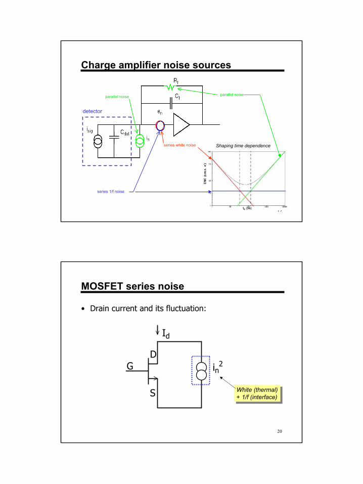
Charge amplifier noise sources
detector
series white noise
parallel noiseparallel noise
series 1/f noise
Shaping time dependence
20
• Drain current and its fluctuation:
in2
D
S
G
Id
White (thermal) + 1/f (interface)
White (thermal) + 1/f (interface)
MOSFET series noise
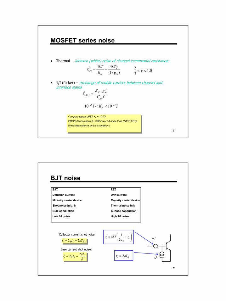
11
21
MOSFET series noise
• Thermal – Johnson (white) noise of channel incremental resistance:
• 1/f (flicker) – exchange of mobile carriers between channel and interface states
)/1(442
,meq
thn gkT
RkTi γ
== 0.132
<< γ
fCgKi
gs
mFfn
22
/1,⋅
=
J10J10 2326 −− << FK
Compare typical JFET KF ~ 10-27J
PMOS devices have 3 - 30X lower 1/f noise than NMOS FETs
Weak dependence on bias conditions.
Compare typical JFET KF ~ 10-27J
PMOS devices have 3 - 30X lower 1/f noise than NMOS FETs
Weak dependence on bias conditions.
22
BJT noiseBJT FET
Diffusion current Drift current
Minority carrier device Majority carrier device
Shot noise in IC, IB Thermal noise in ID
Bulk conduction Surface conduction
Low 1/f noise High 1/f noise
en2
in2
mCc kTgqIi 222 ==
βC
BbqIqIi 222 ==
+= b
mn r
gkTe
2142
Bn qIi 22 =
Collector current shot noise:
Base current shot noise:

12
23
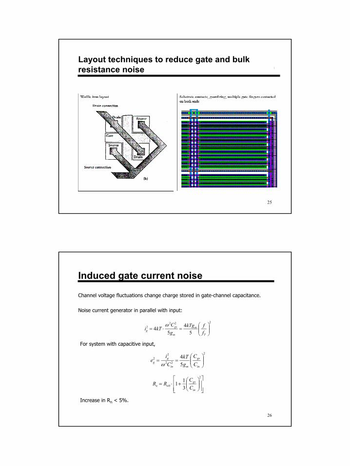
Gate resistance noise
• Polysilicon gate is resistive:– ρpoly 25 Ω/sq.
– ρsilicided poly 4 Ω/sq.
LWR polyg ⋅= ρ
22
124
nR
kTe gng ⋅
⋅=
24
Bulk resistance noise• Resistive substrate couples to the channel via the back
transconductance gmb.• Substrate resistance is distributed.
• Minimize by reverse biasing the source-substrate junction.
22
2 44 mbmb
db gWdkT
ng
nWdnkTi ββ =
⋅
⋅⋅= β = geometrical factor
13
25
Layout techniques to reduce gate and bulk resistance noise
26
Induced gate current noise
Channel voltage fluctuations change charge stored in gate-channel capacitance.
Noise current generator in parallel with input:
2222
54
54
=⋅=
T
m
m
gsg f
fkTggC
kTiω
For system with capacitive input,
2
22
22
54
==
in
gs
min
gg C
CgkT
Ci
eω
+⋅=
2
0 311
in
gsnn C
CRR
Increase in Rn < 5%.
14
27
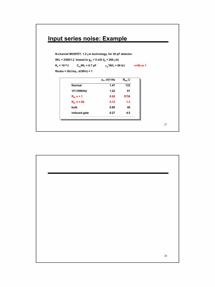
Input series noise: Example
N-channel MOSFET, 1.2 µm technology, for 20 pF detector.
W/L = 3300/1.2 biased to gm = 5 mS (ID = 200 µA)
KF = 10-24J CoxWL = 6.7 pF ρg*W/L = 69 kΩ n=66 or 1
Rsubs = 2kΩ/sq., d/(W/n) = 1
en, nV/√Hz Req, Ω
thermal 1.47 133
1/f (100kHz) 1.22 91
Rg, n = 1 9.60 5750
Rg, n = 66 0.15 1.3
bulk 0.80 40
induced gate 0.27 4.5
28
15
29
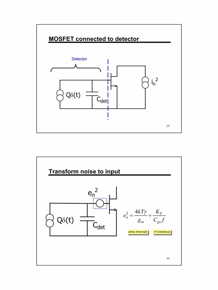
Cdet
in2
Qδ(t)
Detector
MOSFET connected to detector
30
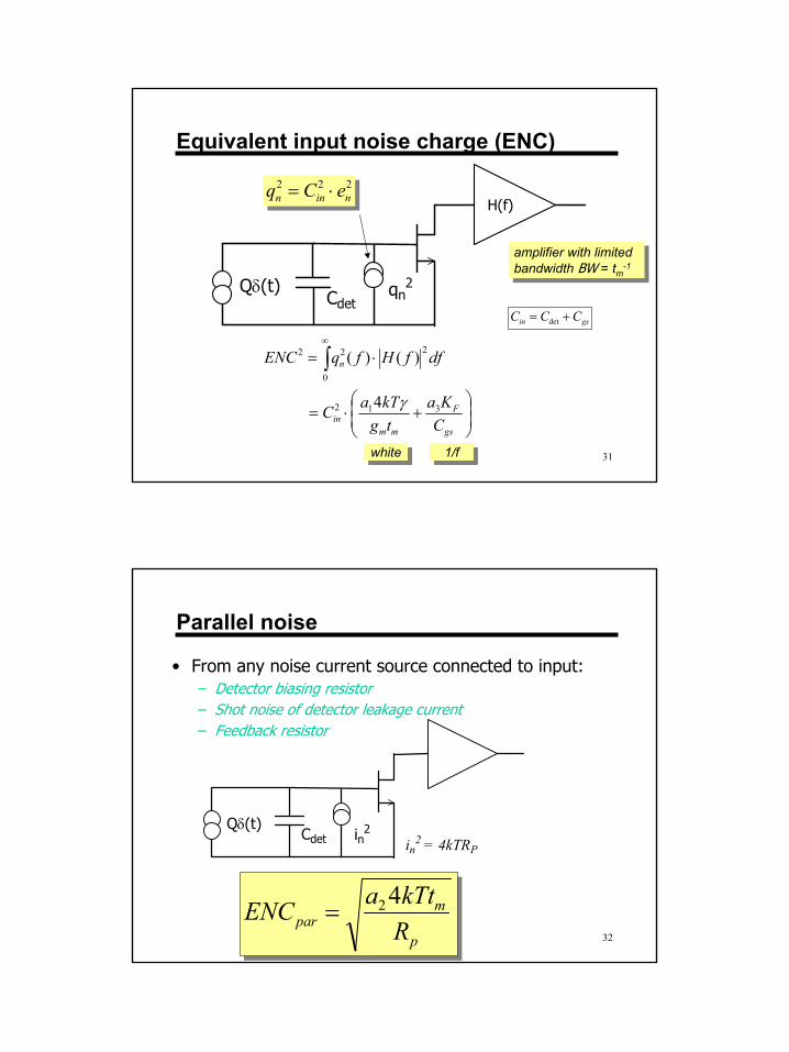
Cdet
en2
Qδ(t) fCK
gkTe
gs
F
mn +=
γ42
Transform noise to input
white (thermal)white (thermal) 1/f (interface)1/f (interface)
16
31
Cdetqn
2Qδ(t)
amplifier with limitedbandwidth BW = tm-1
amplifier with limitedbandwidth BW = tm-1
+⋅=
⋅= ∫∞
gs
F
mmin
n
CKa
tgkTaC
dffHfqENC
312
0
222
4
)()(
γ
Equivalent input noise charge (ENC)
whitewhite 1/f1/f
H(f)222ninn eCq ⋅=
gsin CCC += det
32
• From any noise current source connected to input:– Detector biasing resistor– Shot noise of detector leakage current– Feedback resistor
p
mpar R
kTtaENC 42=
CdetQδ(t)
in2 = 4kTRPin
2
Parallel noise
17
33
Sizing the input transistor for minimum series noise
IDen
CgsCdet
M1 (W,L)
M1 should have minimum L for best gm/Cgs ratio
Increasing M1 width makes en smaller while Cgs gets larger
⇒ an optimum width for M1 must exist
To calculate this optimum (see Appendix I), consider two cases:
I. The FET is biased at constant current density (ID/W = const.)
II. The FET drain current is kept constant as the width W is varied
Case I is simple and the solution is the same as that derived for JFET amplifiers in the 1950’s.
Cgs, opt = Cdet
Case II requires us to look in more detail at how the MOSFET transconductance behaves as the width (and hence the current density) varies.
( )
+
⋅⋅+=
gs
F
mmgs C
Ktg
kTCCENC γ42det
2
34
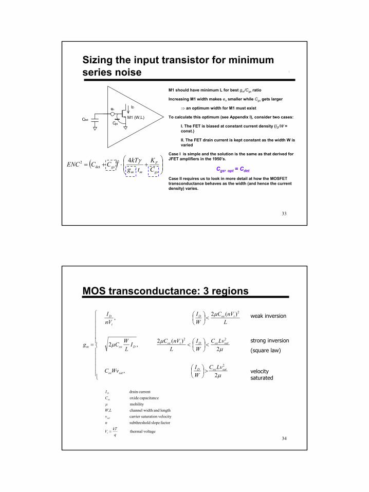
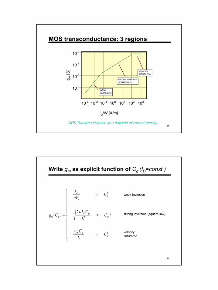
MOS transconductance: 3 regions
>
<
<
<
=
2,
2)(2,2
)(2,
2
22
2
LvCWIWvC
LvCWI
LnVCI
LWC
LnVC
WI
nVI
g
satoxDsatox
satoxDtoxDox
toxD
t
D
m
µ
µµµ
µ weak inversion
strong inversion
(square law)
velocity saturated
voltage thermal
factor slope ldsubthresho velocitysaturationcarrier
length and widthchannel mobility
ecapacitanc oxide current drain
qkTV
nvW,LµCI
t
sat
ox
D
=
18
35
MOS transconductance: 3 regions
MOS Transconductance as a function of current density
36
Write gm as explicit function of Cg (ID=const.)
∝
∝
∝
=
1
2/12
0
2
)(
ggsat
ggD
gt
D
gm
CLCv
CL
CI
CnVI
Cgµ
weak inversion
strong inversion (square law)
velocity saturated
19
37
( )mgm
g
tCgCC
ENC⋅
+=
)(
2det2 α
0)()(2
)()(
2
2detdet
2
=⋅
′+−+=
mm
mgmg
g tggCCgCC
CdENCd αα
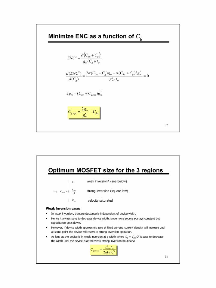
′+= moptgm gCCg )(2 ,det
Minimize ENC as a function of Cg
det,2 CggCm
moptg −
′=
38
Optimum MOSFET size for the 3 regions
⇒
=
det
det, 3
0
C
CC optg
weak inversion* (see below)
strong inversion (square law)
velocity saturated
Weak inversion case:• In weak inversion, transconductance is independent of device width.
• Hence it always pays to decrease device width, since noise source en stays constant but capacitance goes down.
• However, if device width approaches zero at fixed current, current density will increase until at some point the device will revert to strong inversion operation.
• As long as the device is in weak inversion at a width where Cg = Cdet/3, it pays to decrease the width until the device is at the weak-strong inversion boundary:
( )22min
, 2 t
Dwigopt nV
ILCµ
=
20
39
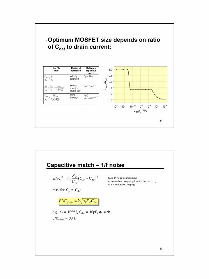
Optimum MOSFET size depends on ratio of Cdet to drain current:
10-12 10-11 10-10 10-9 10-8 10-7 10-6
Cdet/ID [F/A]
0.0
0.2
0.4
0.6
0.8
1.0
Cg,
opt/C
det
Cdet / ID ratio
Region of operation
Optimum capacitive
match
Velocity saturated
Cgs = Cdet
( )22mindet
2 236
tDsat nVL
IC
v µµ
<< Strong-inversion square-law
Cgs = Cdet / 3
Weak inversion
Cgs = Lmin
2ID/2µ(nVT)2
2det 6
satD vIC µ
<
( )22mindet
23
tD nVL
IC
µ>
40
Capacitive match – 1/f noise
min. for Cgs = Cdet:
e.g. KF = 10-24 J, Cdet = 10pF, a3 = 4:
ENCf,min = 80 e-
KF is 1/f noise coefficient (J)a3 depends on weighting function but not on tm.a3 = 4 for CR-RC shaping
det3min, 2 CKaENC Ff =
2det3
2 )( CCCKaENC gs
gs
Ff +=

21
41
• Cdet = 3 pF• tm = 1 µs• Pdiss = 1 mW• Ileak = 100 pA• Technology: 0.35 µm
NMOS
• Optimum width for series noise is a compromise between white and 1/f components
Min.
Composite noise
thermal
42
Minimum series noise
• Input MOSFET fully optimized:
• Key ingredients for low series ENC:– low Cdet
– long tm– short τel
– low KF
det,/1
det,
CKENC
tkTCENC
Foptf
m
eloptsw
≈
≈τ
mgs
el
gC / gate under the
ime transit telectron
=
=τ
22
43
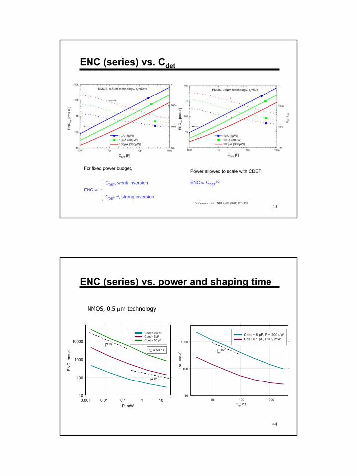
ENC (series) vs. Cdet
For fixed power budget,
CDET, weak inversionENC ∝
CDET3/4, strong inversion
Power allowed to scale with CDET:
ENC ∝ CDET1/2
De Geronimo et al. , NIM A 471 (2001) 192 - 199
44
ENC (series) vs. power and shaping time
0.001 0.01 0.1 1 10P, mW
10
100
1000
10000
ENC
, rm
s e-
Cdet = 0.5 pFCdet = 5pFCdet = 50 pF
tm = 50 ns
10 100 1000tm, ns
10
100
1000
ENC
, rm
s e-
Cdet = 5 pF, P = 200 uWCdet = 1 pF, P = 2 mW
P1/2
P1/4
tm1/2
NMOS, 0.5 µm technology

23
45
Input device optimization for BJT
Bertuccio et al. , NIM A 409 (1998) 286 - 290
βmC
mC
T tIatIkTCaENC 2
22
12 )(
+=m
ToptC qt
kTCaaI β
2
1, =
TkTCaaENC ⋅=β
21min
4series whitecollector current shot noise
series whitecollector current shot noise
parallelbase current shot noise
parallelbase current shot noise
46
MOS vs. BJT front end
• MOS is favored over BJT for low noise when
2
22
m
gs
FD t
LCKkTI
µ
>
MOSdominated noise white 38
2,BJT
MOSel
m
at β
τ>
BJTmDmm
at
CLI
Ctg βµ
2det2
det 382
>=
MOSdominated noise 1/f 21
3
,BJT
MOSF aaa
KkT β>
• MOS is favored for long tm, low Cdet, high power, and short gate length technology.
• MOS 1/f limit always superior to BJT if power budget is high enough:
24
47
48
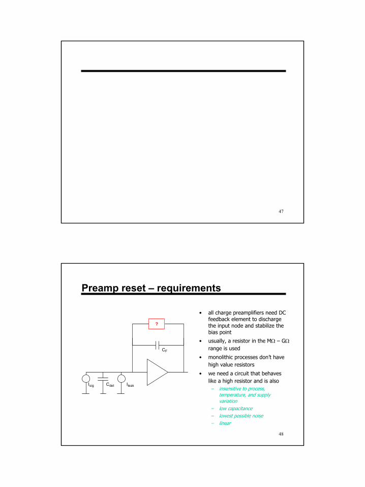
Preamp reset – requirements
• all charge preamplifiers need DC feedback element to discharge the input node and stabilize the bias point
• usually, a resistor in the MΩ – GΩrange is used
• monolithic processes don’t have high value resistors
• we need a circuit that behaves like a high resistor and is also
– insensitive to process, temperature, and supply variation
– low capacitance– lowest possible noise– linear
Cdet
CF
?
Isig Ileak

25
49
Preamplifier reset – monolithic techniques (1)
Physical resistor- always accompanied by parasitic capacitance- de-stabilizes circuit and increases noise- noise higher than 4kT/R by factor ~ RC/tm
Pulsed reset by MOS switch- sampled noise √kTCF- Qinj noise from switch control voltage- leakage current integrates on output node dVout/dt = IL/CF
50
Preamplifier reset – monolithic techniques (2)

26
51
Preamplifier reset – monolithic techniques (3)
52
• Classical– RF · CF = RC ·CC– Zero created by RC,CC cancels
pole formed by RF, CF
• IC Version– CC = N · CF– (W/L)MC = N · (W/L)MF
– Zero created by MC, CC cancels pole formed by MF, CF
– Rely on good matching characteristics of CMOS FETs and capacitors
IN
CCCF
A1 A2
RF RC
VG
IN
CC
MC
CF
MF
A1 A2
G. Gramegna, P. O’Connor, P. Rehak, S. Hart, “CMOS preamplifier for low-capacitance detectors”, NIM-A 390, May 1997, 241 – 250.
Nonlinear pole-zero compensation

27
53
Secondary noise sources in the preamp
– iB12 and iB2
2 are effectively in parallel with the input transistor
– Their contribution to input (white) thermal series noise is (gmB1/gm1)2.
– We minimize their gm w.r.t. that of M1
– gmB1,2 = √2µCoxWID/L
– use low W/L (i.e. long-gate) devices with large or degenerate with source resistor.
– Keep W/L as small as possible (thus Vgs-VT large) while keeping VDS > Vgs-VT.
– Various ways to optimize.
54
Preamplifier Design – Summary
• Optimum noise performance requires selecting, biasing, dimensioning, and laying out the input device properly.
• Bipolar transistor is favored input device for fast, low-power front ends.
• Noise scaling:
• A substantial design effort is needed to realize a low-noise, high-linearity reset system in monolithic technology.
detγβ
α
PtCENCm
∝
5.025.05.0
175.0
<<≈
<<
γβ
α

28
55
56
• Limits the bandwidth for noise• Gives controlled pulse shape appropriate for rate• Control baseline fluctuations• Bring charge-to-voltage gain to its final value• By its saturation characteristics, sets upper limit on Qin
• Feedback circuits give the most stable and precise shaping – At the expense of power dissipation– Poor tolerance of passives limits accuracy of the poles and zeros
• High-order shapers give the lowest noise for a given pulse width
Sallen-Key Lowpass
R1 R2
C1
C2
K
Bridged-T Lowpass
C1
C2
Multiple Feedback Lowpass
R3
R1 R2
C1
C2
1/(s+a) 1/(s+a)1/(s+a)
R1
R2
R3
R4
Follow-the-leader
Filter topologies
Integrated shaping amplifiers

29
57
Pulse shaping filters with real polesSimplest filter: CR-RC
CR-RCn, unipolar semiGaussian
CR2-RCn, bipolar semiGaussian
• asymmetric response
• Identical real poles• Symmetry improves with order n:
• Area-balanced• Derivative of CR-RCn
increasing n
58
Shaper Pole Positions
-6
-4
-2
0
2
4
6
-10 -8 -6 -4 -2 0
MHz
Gaussian CR2RC6
Ohkawa synthesis method (Ohkawa, NIM 138 (1976) 85-92, "Direct Syntheses of the Gaussian Filter for Nuclear Pulse Amplifiers")
For given filter order, gives closest approx. to a true Gaussian
More symmetrical than CR-RCn filter of same order for same peaking time
Noise weighting functions:
I1,complex/I1,CR-RC = 1.18 series
I2,complex/I2,CR-RC = 0.81 parallel
Complex pole approximation to Gaussian pulse

30
59
7th order complex
12th order CR-RCn
Equal peaking times, equal order
7th order complex
7th order CR-RCn
Equal 1% widths, equal order
7th order complex
7th order CR-RCn
Equal peaking times, equal 1% widths
Complex shapers -- advantages
60
Power requirements
• Fundamental limit – power per pole
• Stable, low distortion filters cannot use active element for setting pole frequency⇒ Require higher GBW amplifiers, more power
• Use topologies that realize more than one pole per amplifier• Trim time constants using digitally switched passive elements
noisesignalpeak frequency pole :
,8
0
0
=≅
⋅≥
DRt
nf
DRkTfP
m
pole
pole
31
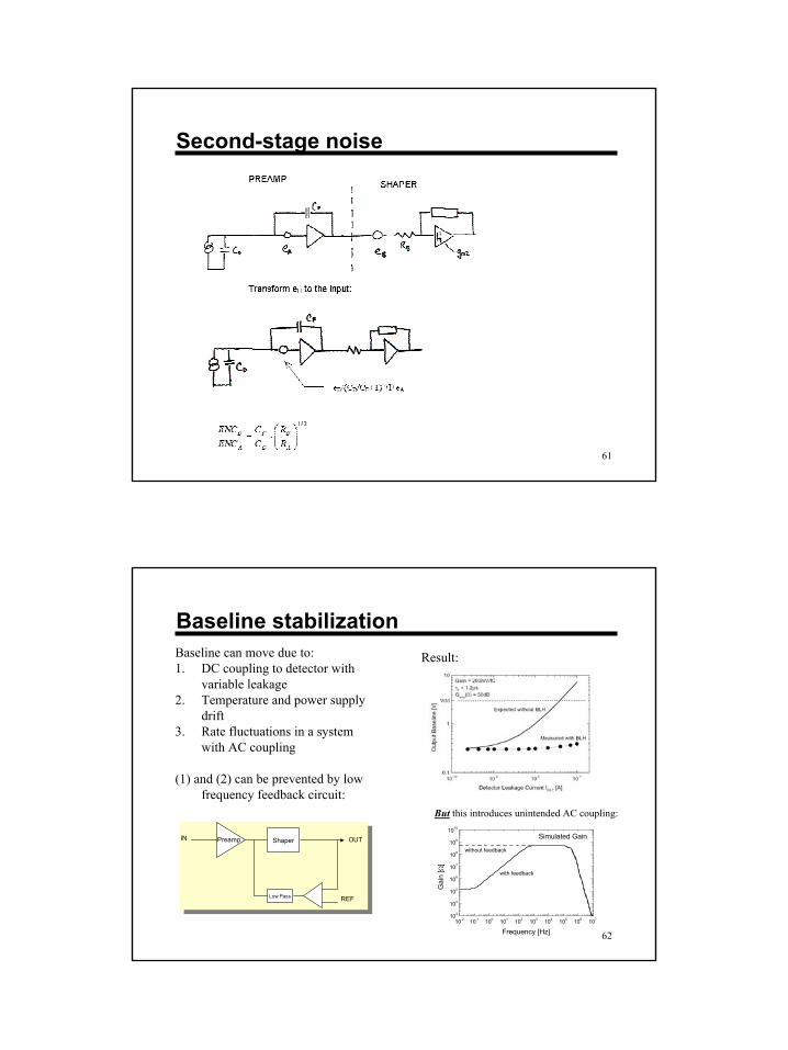
61
Second-stage noise
62
Baseline stabilization
Shaper
Low Pass
PreampIN OUT
REF
10-2 10-1 100 101 102 103 104 105 106 107103
104
105
106
107
108
109
1010
Simulated Gain
with feedback
without feedback
Gai
n [Ω
]
Frequency [Hz]
Baseline can move due to:1. DC coupling to detector with
variable leakage2. Temperature and power supply
drift3. Rate fluctuations in a system
with AC coupling
(1) and (2) can be prevented by low frequency feedback circuit:
Result:
But this introduces unintended AC coupling:

32
63
Baseline holderIntroduce a nonlinear element into the feedback loop:
After a long train of pulses the baseline stays constant:
with BLH
no BLH
64
33
65
Outline
• Custom monolithic front ends– advantages– access to technology– design tools
• Low noise analog design in monolithic CMOS– preamplifier design– shaping amplifier
• Circuit examples• CMOS Scaling and Charge Sensitive Amplifier design
– noise mechanisms in scaled devices– optimum capacitive match to detector– noise, dynamic range, and power vs. scaling length
66
Charge Amplifier based on Silicon MOSFET (1967)
V. Negro et al., “A Guarded Insulated Gate Field Effect Electrometer”, IEEE Trnas. Nucl. Sci. Feb. 1967, 135 – 142
J.B. McCaslin, “A Metal-Oxide-Semiconductor Electrometer Ionization Chamber”, UCRL-11405 (1964)
34
67
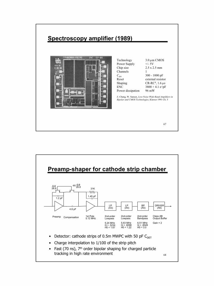
Spectroscopy amplifier (1989)
Technology 3.0 µm CMOSPower Supply +/- 5VChip size 2.5 x 2.5 mmChannels 1Cdet 300 - 1000 pFReset external resistorShaping CR-RC4, 1.6 µsENC 3800 + 4.1 e-/pFPower dissipation 96 mW
Z. Chang, W. Sansen, Low-Noise Wide-Band Amplifiers in Bipolar and CMOS Technologies, Kluwer 1991 Ch. 5
68
Preamp-shaper for cathode strip chamber
LP(A3)
Preamp Compensation 1st Pole5.12 MHz
2nd-orderLowpass
5.24 MHzQ = .5234H0 = 1.67
LP(A4)
2nd-orderLowpass
5.63 MHzQ = .6098H0 = 1.22
BP(A5)
2nd-orderBandpass
6.51 MHzQ = .8549H0 = 3.0
DRIVER(A6)
Class ABOutput Buffer
Gain = 2
1.2 pF
4.8 pF
1.45 pF
31K0.928.8
0.928.84X
• Detector: cathode strips of 0.5m MWPC with 50 pF CDET
• Charge interpolation to 1/100 of the strip pitch• Fast (70 ns), 7th order bipolar shaping for charged particle
tracking in high rate environment

35
69
200 100 0 100 200 300 4001
0.5
0
0.5
1
Time (ns)
Vou
t
Pulse Shape simulated (solid red line) and measured (blue dotted line)
0
0.5
1
1.5
2
2.5
0 200 400 600Qin (fC)
Vou
t (V
)
Simulated: ωMeasured: o
0 20 40 60 80 100 1201000
1500
2000
2500
3000
3500
Cd (pF)
ENC
(rm
s e-)
470 pF
100 ΩUNLOADED
Preamp-shaper for Cathode Strip Chamber
70
• Used with ultra-low capacitance silicon drift detector, Cdet < 0.3 pF
• Preamp only, used with external shaper
• Purpose: explore lowest noise possible with CMOS
• Reset system: MOS transistor with special bias circuit to achieve stable, > 100 GΩ equivalent resistance
Detector
Drift detector preamplifier

36
71
Drift detector preamplifier – simplified schematic
72
Drift detector & CMOS preamplifier
37
73
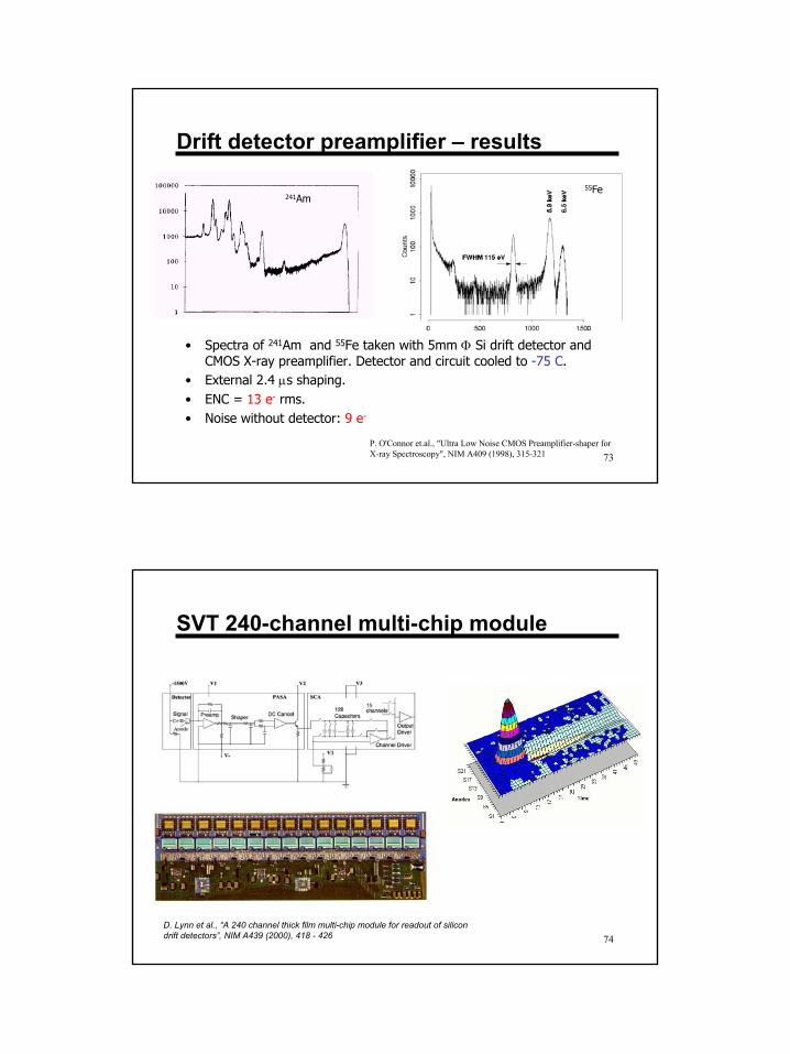
• Spectra of 241Am and 55Fe taken with 5mm Φ Si drift detector and CMOS X-ray preamplifier. Detector and circuit cooled to -75 C.
• External 2.4 µs shaping.• ENC = 13 e- rms.• Noise without detector: 9 e-
P. O'Connor et.al., "Ultra Low Noise CMOS Preamplifier-shaper for X-ray Spectroscopy", NIM A409 (1998), 315-321
241Am55Fe
Drift detector preamplifier – results
74D. Lynn et al., “A 240 channel thick film multi-chip module for readout of silicon drift detectors”, NIM A439 (2000), 418 - 426
SVT 240-channel multi-chip module

38
75
PROJECT Hi-res. Spectroscopy
RHIC – PHENIX RHIC – STAR LHC – ATLAS Industry Partnership
NSLS – HIRAX Units
DETECTOR Si drift Time Expansion Chamber
Silicon Vertex Tracker
Cathode Strip Chamber
CdZnTe gamma ray detector
Si Pixel
Function Preamp Preamp/Shaper Preamp/Shaper Preamp/Shaper Preamp/Shaper Preamp/Shaper/Counter
CDET 0.3 30 3 50 3 1.5 pF Peaking Time
2400 70 50 70 600:1200:2000:4000
500:1000:2000:4000
ns
Gain 10 2.4:12 – 10/25 40:70:90 4 30:50:100:200 750:1500 mV/fC Power 10 30 3.8 33 18 7 mW/channel ENC 10 1250 400 2000 100 24 rms electrons Dynamic Range
1250 4600 700 1900 5600
Technology CMOS 1.2 um CMOS 1.2 um Bipolar 4 GHz CMOS 0.5 um CMOS 0.5 um CMOS 0.35 um Input Transistor
PMOS 150/1.2 um
NMOS 4200/1.2 um
NPN 10 uA
NMOS 5000/0.6 um
NMOS 200/0.6 um
PMOS 400/0.4 um
Reset Scheme
Compensated PMOS, > 1GΩ
Polysilicon, 75 kΩ
Nwell, 250 kΩ
Compensated NMOS, 30 MΩ
Compensated PMOS
Compensated NMOS
No. Channels
6 8 16 24 16 32
Die Size 7.3 15 8 20 19 16 mm2
BNL Preamp/Shaper ICs, 1995 - 2001
76
• Preamplifier reset• High order filters• Programmable pulse
parameters• Circuit robustness:
– Self-biasing– Low-swing,differential I/O
– Circuits tolerant to variations in• Temperature• Process • Power supply• DC leakage current• Loading
• Preamplifier reset• High order filters• Programmable pulse
parameters• Circuit robustness:
– Self-biasing– Low-swing,differential I/O
– Circuits tolerant to variations in• Temperature• Process • Power supply• DC leakage current• Loading
Pulse vs. Temperature
0 2x10⁻⁶ 4x10⁻⁶ 6x10⁻⁶ 8x10⁻⁶
0.0
0.5
1.0
1.5
2.0Programmable Dual Stage N=24x6Cin≈1.5pF, Qdet≈10fC
Sign
al [V
]
Time [s]
Gain variation
0 2x10⁻⁶ 4x10⁻⁶ 6x10⁻⁶ 8x10-
0.0
0.5
1.0
1.5
2.0
2.5
Dual Stage N = 24x6CIN ≈ 3pFQIN ≈ 11fCGain ≈ 200mV/fCIdet ≈ 250pA ÷ 70nA
Out
put S
igna
l [V]
Time [s]0.0 3.0x10⁻⁶ 6.0x10⁻⁶ 9.0x10⁻⁶ 1.2x10⁻⁵ 1.5x10⁻⁵
0.0
0.5
1.0
1.5
2.0
2.5
Programmable Dual StageCIN ≈ 1.5pF, QDET ≈ 12fC
Cha
nnel
Out
put [
V]
Time [s]
Peaking time variation
G. De Geronimo et al., “A generation of CMOS readout ASICs for CZT detectors", IEEE Trans. Nucl. Sci. 47, Dec. 2000, 1857 - 1867
Practical amplifier considerations
Pulse vs. Ileak

39
77
78
Outline
• Custom monolithic front ends– advantages– access to technology– design tools
• Low noise analog design in monolithic CMOS– preamplifier design– shaping amplifier
• Circuit examples• CMOS Scaling and Charge Sensitive Amplifier design
– noise mechanisms in scaled devices– optimum capacitive match to detector– noise, dynamic range, and power vs. scaling length

40
79
Scaling issues
• Fundamental device noise mechanisms– Hot electron effects– New process steps effect on 1/f noise– Gate tunneling current
• Change of the current-voltage characteristics– Increase of weak inversion current– Mobility decrease– Velocity saturation– Drain conductance (device intrinsic DC gain)
• Power supply scaling
80
CMOS Scaling
• Driven by digital VLSI circuit needs
• Goals: in each generation– 2X increase in
density– 1.5X increase in
speed– Control short channel
effects– Maintain reliability
level of < 1 failure in 107 chip-hours
2b 64Kb 64Mb 2.3 mm 2 26 mm 2 198 mm 2
1960s 1980s 1990s
40048008
DRAM
Intel microprocessor
41
81
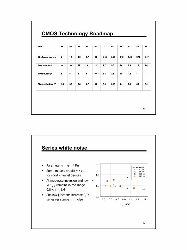
CMOS Technology Roadmap
Year 85 88 91 94 97 00 02 04 07 10 13
Min. feature size [µm] 2 1.5 1.0 0.7 0.5 0.35 0.25 0.18 0.13 0.10 0.07
Gate oxide [nm] 44 33 22 16 11 7.7 5.5 4.0 2.9 2.2 1.6
Power supply [V] 5 5 5 5 5/3.3 3.3 2.5 1.8 1.2 1 .7
Threshold voltage [V] 1.0 0.9 0.8 0.7 0.6 0.5 0.45 0.4 0.3 0.3 0.3
Year 85 88 91 94 97 00 02 04 07 10 13
Min. feature size [µm] 2 1.5 1.0 0.7 0.5 0.35 0.25 0.18 0.13 0.10 0.07
Gate oxide [nm] 44 33 22 16 11 7.7 5.5 4.0 2.9 2.2 1.6
Power supply [V] 5 5 5 5 5/3.3 3.3 2.5 1.8 1.2 1 .7
Threshold voltage [V] 1.0 0.9 0.8 0.7 0.6 0.5 0.45 0.4 0.3 0.3 0.3
YearYear 8585 8888 9191 9494 9797 0000 0202 0404 0707 1010 1313
Min. feature size [µm]Min. feature size [µm] 22 1.51.5 1.01.0 0.70.7 0.50.5 0.350.35 0.250.25 0.180.18 0.130.13 0.100.10 0.070.07
Gate oxide [nm]Gate oxide [nm] 4444 3333 2222 1616 1111 7.77.7 5.55.5 4.04.0 2.92.9 2.22.2 1.61.6
Power supply [V]Power supply [V] 55 55 55 55 5/3.35/3.3 3.33.3 2.52.5 1.81.8 1.21.2 11 .7.7
Threshold voltage [V]Threshold voltage [V] 1.01.0 0.90.9 0.80.8 0.70.7 0.60.6 0.50.5 0.450.45 0.40.4 0.30.3 0.30.3 0.30.3
82
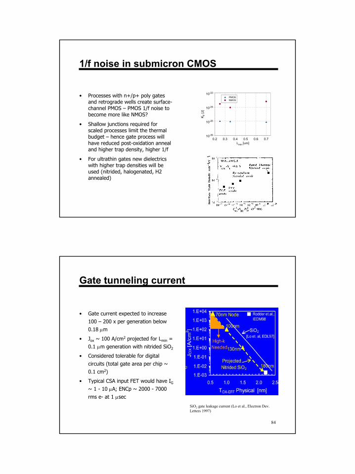
Series white noise
• Parameter γ = gm * Rn
• Some models predict γ >> 1 for short channel devices
• At moderate inversion and low VDS, γ remains in the range 0.8 < γ < 1.4
• Shallow junctions increase S/D series resistance => noise 0.3 0.5 0.7 0.9 1.1 1.3 1.5
Lmin [um]
0.5
1.0
1.5
2.0
γ
0.7 um0.5 um0.35 um0.25 um
TECHNOLOGY:
42
83
1/f noise in submicron CMOS
• Processes with n+/p+ poly gates and retrograde wells create surface-channel PMOS – PMOS 1/f noise to become more like NMOS?
• Shallow junctions required for scaled processes limit the thermal budget – hence gate process will have reduced post-oxidation anneal and higher trap density, higher 1/f
• For ultrathin gates new dielectrics with higher trap densities will be used (nitrided, halogenated, H2 annealed)
0.2 0.3 0.4 0.5 0.6 0.7Lmin [um]
10-26
10-25
10-24
10-23
K F [J
]
PMOSNMOS
84
Gate tunneling current
• Gate current expected to increase 100 – 200 x per generation below 0.18 µm
• Jox ~ 100 A/cm2 projected for Lmin = 0.1 µm generation with nitrided SiO2
• Considered tolerable for digital circuits (total gate area per chip ~ 0.1 cm2)
• Typical CSA input FET would have IG
~ 1 - 10 µA; ENCp ~ 2000 - 7000 rms e- at 1 µsec
SiO2 gate leakage current (Lo et al., Electron Dev. Letters 1997)

43
85
Departure from square-law characteristics
• Submicron devices are less often operated in strong inversion, square-law region.
• By the 0.13 mm generation, the square-law region will vanish altogether
10-3 10-2 10-1 100 101 102 103
ID/W [A/m]
10-6
10-5
10-4
10-3
10-2
g m [S
]
0.18 um0.6 um2.0 um
STRONG INVERSION(SQUARE LAW)
TECHNOLOGY:
VELOCITYSATURATION
WEAKINVERSION
86
10-12 10-11 10-10 10-9 10-8 10-7 10-6
Cdet/ID [F/A]
0.0
0.2
0.4
0.6
0.8
1.0
Cg,
opt/C
det
2.0 um0.6 um0.18 um
TECHNOLOGY:
– Drain current = constant– Ratio of Cgs to Cdet determined by Cdet/Id:
P. O’Connor, G. De Geronimo, “Prospects for Charge Sensitive Amplifiers in Scaled CMOS”, NIM-A accepted for publication
Generalized capacitive matching condition

44
87
Example – strong inversion limits
• NMOS input device
• ID = 250 µA
• 2 µm technology:
– 9.3 fF < Cdet < 26.3 pF
• 0.18 µm technology:
– 9.3 fF < Cdet < 210 fF
88
Capacitive match vs. scaling – mixed white, 1/f and parallel noise
• The contribution of thermal and 1/f changes as technology scales• Example: Cdet = 3 pF, tm = 1 µs, Pdiss = 1 mW, Ileak = 100 pA:
2 µm NMOS2 µm NMOS 0.5 µm NMOS0.5 µm NMOS 0.1 µm NMOS0.1 µm NMOS
thermal thermalthermal
thermal
45
89
Noise vs. scaling for mixed white, 1/f, and parallel noise
0.1 1.0Lmin [um]
101
102
103
ENC
min
[rm
s el
ectro
ns]
a
b
c
d
Noise vs. scaling Optimum gate width vs. scaling
4 detector scenarios for scaling study
b
a
c
0.1 1Lmin [um]
0
0.2
0.4
0.6
0.8
Cg,
opt/C
det
Cg/Cd = 1/3
d
900.1 1.0
Lmin [um]
0.01
0.1
1
10
100
Pow
er [m
W]
d
a
b
c
0.1 1.0Lmin [um]
101
102
103
ENC
min
[rm
s el
ectro
ns]
a
b
c
d
Noise vs. scaling
(power held constant)
Power vs. scaling
(noise held constant)
4 detector scenarios for scaling study
Noise and power vs. scaling

46
91
1.E+03
1.E+04
1.E+05
1.E+06
0.1 1 10
Lmin [um]
Dyn
amic
Ran
ge
a
c
Dynamic range vs. scaling
92
Active Pixel Sensor: radiation detector in standard CMOS
http://www.photobit.com

47
93
CMOS APS for particle detection/tracking
Monolithic –special assembly technology not requiredLow costLow multiple scatteringGood spatial resolution (few µm)Random accessIntegration of control and DSPRadiation tolerance (?)
Special processCollection time scales with pixel sizeCircuit architecture embryonic
94diffusion isochron“photo”
diode
metal
n+
nwell
pwell
poly
Simple monolithic active pixel
VDDRE_SEL
ROW_SEL
CO
LUM
N L
INE
48
95
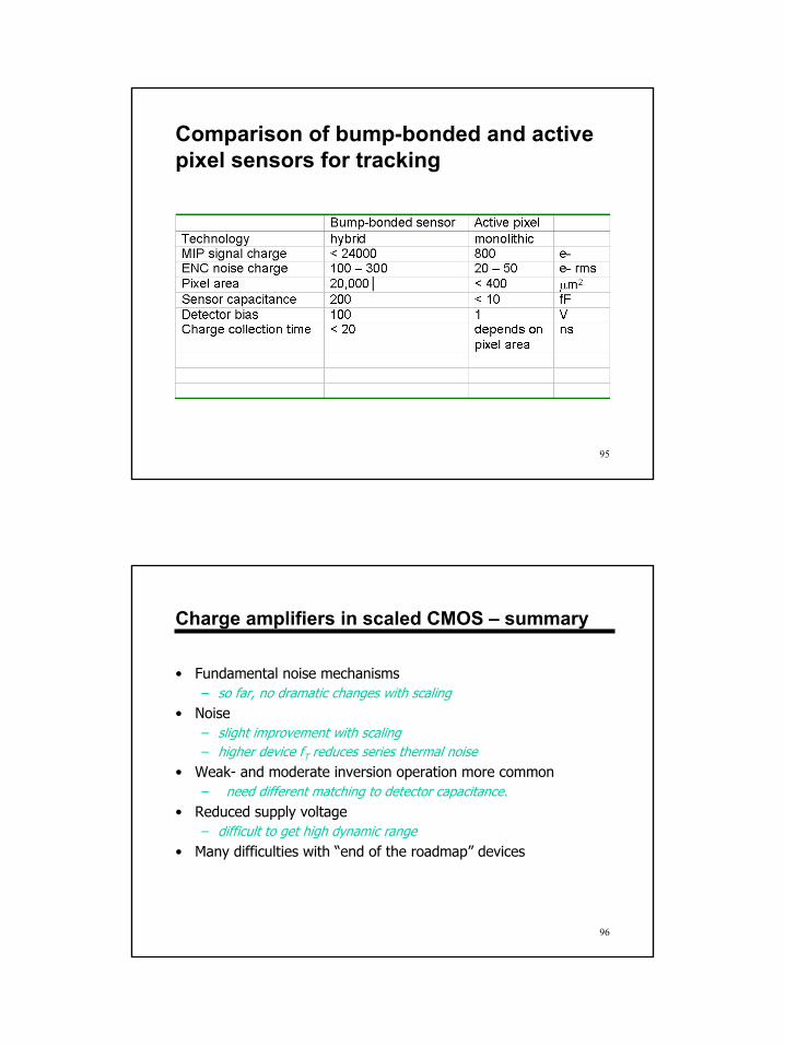
Comparison of bump-bonded and active pixel sensors for tracking
96
Charge amplifiers in scaled CMOS – summary
• Fundamental noise mechanisms– so far, no dramatic changes with scaling
• Noise– slight improvement with scaling– higher device fT reduces series thermal noise
• Weak- and moderate inversion operation more common– need different matching to detector capacitance.
• Reduced supply voltage– difficult to get high dynamic range
• Many difficulties with “end of the roadmap” devices

49
97
98
Summary and Future Directions
• Today’s monolithic technology can be used effectively for low-noise front ends.
• Technology scaling, by reducing the area and power per function, wil allow increasingly sophisticated signal processing on a single die.
• Integrated sensors will be developed for some X-ray and charged-particle tracking applications.
• Interconnecting the front end to the detector and to the rest ofthe system will continue to pose challenges.