chemical vapor deposition of thin film materials for electronic and
TRANSCRIPT
CHEMICAL VAPOR DEPOSITION OF THIN FILM
MATERIALS FOR ELECTRONIC AND
MAGNETIC APPLICATIONS
by
NING LI
TONYA M. KLEIN, COMMITTEE CHAIR
ARUNAVA GUPTA
ALAN M. LANE
SUBHADRA GUPTA
MARK L. WEAVER
A DISSERTATION
Submitted in partial fulfillment of the requirements for the
degree of Doctor of Philosophy in the Department
of Chemical and Biological Engineering
in the Graduate School of
The University of Alabama
TUSCALOOSA, ALABAMA
2011

Copyright Ning Li 2011
ALL RIGHTS RESERVED

ii
ABSTRACT
Chemical vapor deposition (CVD) has been employed to pursue high quality thin film
growth for four different materials with excellent electronic or magnetic properties for certain
device applications. The relationship between CVD processing conditions and various thin film
properties has been systematically studied.
Plasma enhanced atomic layer deposition (PEALD) is a special type of CVD technique
and can be used for the deposition of very thin (few nanometers) and highly conformal thin films.
PEALD of hafnium nitride (HfN) thin film is studied by using tetrakis (dimethylamido) hafnium
(IV) (TDMAH) and hydrogen plasma. Prior to thin film deposition, TDMAH adsorption and
reaction on hydrogenated Si(100) surface has been investigated by in-situ ATR-FTIR. It has been
found that between 100˚C and 150˚C surface adsorbed TDMAH molecules start to decompose
based on the β-hydride elimination mechanism. The decomposition species on the surface has
been found hard to desorb at 150˚C, which can contaminate the thin film if the purging/pumping
time is insufficient. Uniform and moderately conductive HfNxCy films are deposited on
hydrogen terminated Si(100) and thermally grown SiO2 (on Si) substrates by PEALD process.
The dependence of thin film resistivity on plasma power is found to be related to the change of
surface chemical composition. In vacuo XPS depth profile analysis showed the existence of
hafnium carbide phase, which to a certain degree can improve the film conductivity.
Direct liquid injection chemical vapor deposition (DLI-CVD) has been utilized for
epitaxial growth of nickel ferrite (NiFe2O4), lithium ferrite (LiFe5O8) and barium titanate

iii
(BaTiO3) films on various lattice match substrates. For the deposition of nickel ferrite, anhydrous
Ni(acac)2 and Fe(acac)3 (acac = acetylacetonate) are used as precursor sources dissolved in N,N-
dimethyl formamide (DMF) for the DLI vaporizer system. Epitaxial nickel ferrite films of
stoichiometric composition are obtained in the temperature range of 500-800 ºC on both
MgO(100) and MgAl2O4(100). Film morphology is found to be dependent on the deposition
temperature with atomically smooth films being obtained for deposition temperature of 600 and
700 ºC. Magnetic measurements reveal an increase in the saturation magnetization for the films
with increasing growth temperature, which correlates well with the trend for improved epitaxial
growth. Nickel ferrite films deposited on MgAl2O4 (100) at 800ºC exhibit saturation
magnetization very close to the bulk value of 300 emu/cm3. Out-of-plane FMR measurement
shows the narrowest FMR line width of ~160 Oe for films deposited at 600˚C. For lithium ferrite
deposition, anhydrous Li(acac) and Fe(acac)3 are dissolved in DMF in a molar ratio of 1:5.
Epitaxial growth of lithium ferrite films on MgO(100) are observed in the temperature range of
500˚C to 800˚C. The as grown films show increasing saturation magnetization with increasing
deposition temperature due to the improved degree of crystal texture. For barium titanate thin
film deposition, Ba(hfa)2•tetraglyme and Ti(thd)2(OPri)2 are dissolved in toluene in a molar ratio
of 1:1. Epitaxial growth of barium titanate on MgO(100) has been found at the temperature of
750˚C. Film with a thickness of ~500 nm has a relatively large roughness of ~20 nm. Small
amount of F elements, which exists in Ba-F bonds, has been detected in the thin film by XPS.

iv
DEDICATION
This dissertation is dedicated to everyone who helped me and guided me through the
trials and tribulations of creating this manuscript. In particular, my family and close friends who
stood by me throughout the time taken to complete this masterpiece.

v
LIST OF ABBREVIATIONS AND SYMBOLS
a, b, c, Lattice parameters
AFM Atomic force microscopy
AGM Alternating gradient magnetometer
ALD Atomic layer deposition
at% Atomic percentage
a.u. Arbitrary units
B Magnetic induction
BDE Bond dissociation energy
BTO Barium titanate (BaTiO3)
C Light speed or capacitance
CVD Chemical vapor deposition
d Lattice plane spacing
D Diffusivity
δ Conductivity or boundary layer
DI Deionized water
DOE Design of experiments
DRAM Dynamic random access memory
E Energy or electric field
EDX Energy dispersive X-ray spectroscopy
EF Fermi energy

vi
φ In-plane tilt angle of X-ray diffraction measurement
FET Field effect transistor
FMR Ferromagnetic resonance
g Effective g factor
GPC Growth per cycle
γ Geromagnetic ratio
GMR Giant magnetoresistance
HC Coercivity field
h Planck constant
[h k l] Miller indices for a direction indexed by h along x axis, k along y axis, and l
along z axis
(h k l) Miller indices for a plane normal to the [h k l] direction
IC Integrated circuit
λ Light wavelength
LFO Lithium ferrite (LiFe5O8)
LPCVD Low pressure CVD
M Magnetization
MS Saturation magnetization
MBE Molecular beam epitaxy
MOCVD Metal organic chemical vapor deposition
MR Magnetoresistance
MRAM Magnetic random access memory
μB Bohr magneton

vii
NFO Nickel ferrite (NiFe2O4)
ω Angular frequency or angle in transverse X-ray diffraction measurement
P Polarization
PECVD/ALD Plasma enhanced chemical vapor depostion/atomic layer deposition
PLD Pulsed laser deposition
ψ Longitudinal tilting angle in X-ray diffraction measurement
RF Radio frequency
RMS Root mean square
σ Photoelectric cross section
θ Angle
s, p, d, f electron subshells
SEM Scanning electron microscopy
T Temperature
Tc Curie temperature
TDMAH Tetrakis (dimethylamido) hafnium
TEM Transmission electron microscopy
TMR Tunneling magnetoresistance
VSM Vibrating sample magnetometer
UV Ultraviolet light
XPS X-ray photoelectron spectroscopy
XRD X-ray diffraction
XRR X-ray reflectivity
x, y, z Cartesian coordination
viii
ACKNOWLEDGMENTS
It is my pleasure to have this opportunity to express my sincere appreciation to everyone
who gave me help to my research and life during my Ph. D. period. The most important person is
my advisor Dr. Tonya M. Klein, who guided me into the field of chemical vapor deposition of
solid thin film materials. From the basic knowledge of vacuum system design and maintenance
to theoretical understanding of thin film growth behavior, I have been greatly benefited from her
professional guidance and advising. I would like to express deep respects and great thanks for
her patient teaching, invaluable support, and kind trust and encouragement in the past 5 years. I
would like to thank my co-advisor Dr. Arunava Gupta, who directed me into the world of
magnetic/microwave thin film growth and characterization, which greatly improved my
understanding of the relationship between thin film processing conditions and thin film physical
properties. Under his support, I have the opportunity to access various cutting-edge thin film
characterization techniques/equipments. From him, I have learned a lot on the correct research
attitude and the efficient way of analyzing and solving problems.
I would like to thank my committee members: Dr. Alan Lane, Dr. Subhadra Gupta and
Dr. Mark Weaver, who have greatly helped me on certain sample characterization, experimental
equipments and results interpretation. By taking their courses and discussing with them, I have
got a lot of inspirations and learnt how to keep a correct track on my research. Their professional
experience in both materials science and chemical engineering always help me to figure out the
best solutions in my research.

ix
I would also like to express my sincere thanks to Dr. Heath Turner, Dr. Gary Mankey,
Dr. Tim Mewes and Dr. Shane Street. Their kind teaching and help on modeling software,
vacuum equipment and certain film characterization techniques are essential for my research to
run smoothly and efficiently.
I would like to thank all of my lab mates and group members from both Dr. Klein and Dr.
Gupta's group: Dr. Jinwen Wang, Dr. Gihan Kwon, Dr. Kejing Li, Shilpa Dubey, Dr. Yu-Hsiang
A. Wang, Dr. Dipanjan Mazumdar, Dr. Jianxing Ma, Dr. Ningzhong Bao, Dr. Liming Shen, Dr.
Majit Pathak, Xing zhong, Xueyu Zhang, Ziyou Zhou, Cihat Boyraz, Xiaoyan Zhang, and
Mehmet Yurtisigi. It's always my pleasure to work with them and share experimental
experiences with them. The discussion with them greatly broadened my understanding in
materials related knowledge in physics and chemistry.
I would like to thank Mr. John Hawkins from MINT center, Mr. Rich Martens, Mr.
Johnny Goodwin and Mr. Robert Holler from the center of Central Analytical Facility. They
have helped me on learning film characterization techniques and troubleshooting hardware
problems.
Finally, I would like to thank all of my family members, especially my wife, for their
continuous love and support.

x
CONTENTS
ABSTRACT .................................................................................................................................... ii
DEDICATION ............................................................................................................................... iv
LIST OF ABBREVIATIONS AND SYMBOLS ........................................................................... v
ACKNOWLEDGMENTS ........................................................................................................... viii
LIST OF TABLES ....................................................................................................................... xiv
LIST OF FIGURES ...................................................................................................................... xv
CHAPTER 1. INTRODUCTION ................................................................................................... 1
1.1 Chemical Vapor Deposition (CVD) ...................................................................................... 2
1.1.1 Introduction .................................................................................................................... 2
1.1.2 Atomic Layer Deposition (ALD) ................................................................................... 6
1.1.3 Direct Liquid Injection Chemical Vapor Deposition (DLICVD) ................................... 8
1.2 Thin Film Growth and Characterization ............................................................................. 10
1.2.1 Gas Kinetics .................................................................................................................. 10
1.2.2 Thin film growth in a CVD process ............................................................................. 12
1.2.3 Thin Film Characterization ........................................................................................... 17
1.2.3.1 Attenuated Total Reflectance Fourier Transform Infrared Spectroscopy (ATR-
FTIR) ................................................................................................................................. 18
1.2.3.2 X-ray Photoelectron Spectroscopy (XPS) ............................................................. 21

xi
1.2.3.3 X-ray Diffraction (XRD) ....................................................................................... 24
1.2.3.4 Atomic Force Microscopy (AFM) ......................................................................... 26
1.2.3.5 Ferromagnetic Resonance (FMR) .......................................................................... 28
1.3 Thin Film Application in Electronic and Magnetic Devices ............................................... 30
1.3.1 Metal Oxide Field Effect Transistor (MOSFET) ......................................................... 30
1.3.2 Ferrite-Ferroelectric Layered Heterostructures ............................................................ 33
CHAPTER 2. LITERATURE REVIEW ...................................................................................... 35
2.1 Hafnium Nitride (HfN) ........................................................................................................ 35
2.1.1 Physical Properties and Potential Applications ............................................................ 35
2.1.2 Review of HfN Thin Film Growth ............................................................................... 36
2.2 Spinel ferrite: Nickel Ferrite and Lithium Ferrite ............................................................... 39
2.2.1 Physical Properties and Potential Applications ............................................................ 39
2.2.2 Review of thin film growth methods ............................................................................ 41
2.3 Barium Titanate (BaTiO3) ................................................................................................... 44
2.3.1 Physical Properties and Potential Applications ............................................................ 44
2.3.2 Review of thin film growth methods ............................................................................ 45
CHAPTER 3. PLASMA ENHANCED ATOMIC LAYER DEPOSITION OF HAFNIUM
NITRIDE FILMS .......................................................................................................................... 48
3.1 Introduction ......................................................................................................................... 48
3.2 Tetrakis (Dimethylamido) Hafnium (IV) (TDMAH) Adsorption and Reaction on
Hydrogenated Si(100) Surface .................................................................................................. 49

xii
3.2.1 Introduction .................................................................................................................. 49
3.2.2 Experimental Details .................................................................................................... 50
3.2.3 Results and Discussion ................................................................................................. 53
3.3 Plasma Enhanced Atomic Layer Deposition of HfN Films ................................................ 60
3.3.1 Introduction .................................................................................................................. 60
3.3.2 Experimental Details .................................................................................................... 60
3.3.3 Results and Discussion ................................................................................................. 64
3.4 Conclusion ........................................................................................................................... 71
CHAPTER 4. DIRECT LIQUID INJECTION CHEMICAL VAPOR DEPOSITION OF
FERRIMAGNETIC NICKEL FERRITE AND LITHIUM FERRITE FILMS ............................ 72
4.1 Introduction ......................................................................................................................... 72
4.2 DLI-CVD Growth of NiFe2O4 Films .................................................................................. 73
4.2.1 Experimental Details .................................................................................................... 75
4.2.2 Results and Discussion ................................................................................................. 78
4.2.2.1 Thin Film Growth on MgAl2O4 (100) and MgO (100) ......................................... 78
4.2.2.1.1 Oxygen Effect on Film Morphology ............................................................... 78
4.2.2.1.2 Thin Film Growth Mode ................................................................................. 80
4.2.2.1.3 Physical properties .......................................................................................... 84
4.2.2.2 Thin Film Growth on MgO(111), STO(100), PMN-PT(100) and PZN-PT(100) . 96
4.3 DLI-CVD Growth of LiFe5O8 Films ................................................................................. 100
4.4 Conclusion ......................................................................................................................... 104

xiii
CHAPTER 5. DIRECT LIQUID INJECTION CHEMICAL VAPOR DEPOSITION OF
FERROELECTRIC BARIUM TITANATE FILMS .................................................................. 106
5.1 Introduction ....................................................................................................................... 106
5.2 Experimental Details ......................................................................................................... 107
5.3 Results and Discussion ...................................................................................................... 109
5.4 Conclusion ......................................................................................................................... 113
CHAPTER 6. CONCLUSION AND FUTURE WORK ............................................................ 114
6.1 Conclusion ......................................................................................................................... 114
6.1.1 PEALD of HfN thin films .......................................................................................... 114
6.1.2 DLI-CVD of nickel ferrite and lithium ferrite films................................................... 115
6.1.3 DLI-CVD of barium titanate films ............................................................................. 117
6.2 Future work ....................................................................................................................... 117
REFERENCES ........................................................................................................................... 119
APPENDIX A: LabVIEW PROGRAM FOR PEALD AUTOMATIC PROCESS ................... 128
APPENDIX B: TDMAH MOLECULAR STRUCTUR OPTIMIZATION AND IR
FREQUENCY CALCULATION ............................................................................................... 130
xiv
LIST OF TABLES
Table 1. Hafnium amide precursors and their properties...............................................................38
Table 2. In vacuo XPS results of thin film surface chemical composition at different
experimental conditions..................................................................................................67
Table 3. Chemical composition change with depth of analysis.....................................................69
Table 4. Typical processing conditions for DLI CVD of epitaxial NiFe2O4 films........................79
Table 5. Characteristics of nickel ferrite films deposited at different substrate temperatures.......84
Table 6. Structural and magnetic properties of nickel ferrite films deposited at
different temperatures....................................................................................................98
Table 7. Typical vaporization and processing conditions for DLI CVD of epitaxial
LiFe5O8 films.................................................................................................................106
xv
LIST OF FIGURES
Fig. 1. Schematic of a typical CVD system with a horizontal tube reactor.....................................3
Fig. 2. A typical ALD cycle with oxidation reaction.....................................................................7
Fig. 3. Schematic of a typical direct liquid injection vaporization system....................................10
Fig. 4. Schematic of multiple reflection ART-FTIR spectroscopy................................................20
Fig. 5. Schematic of photoelectron generation process.................................................................21
Fig. 6. Geometric derivation of Bragg's law..................................................................................24
Fig. 7. Schematic of X-ray diffractometer for thin film crystal structure analysis........................25
Fig. 8. Main components of atomic force microscopy system......................................................27
Fig. 9. Magnetic dipole moment precessing about a static magnetic field....................................28
Fig. 10. Schematic of a n-channel MOSFET.................................................................................31
Fig. 11. ME coupling in a ferrite-ferroelectric layered structure...................................................34
Fig. 12. Unit cell of HfN crystal with cubic structure...................................................................35
Fig. 13. (a) Id-Vg and (b) Id-Vd characteristics of an n-MOSFET using HfN-HfO2 gate stack
with EOT 1.18 nm.........................................................................................................................36
Fig. 14. A cross sectional scanning electron micrograph of uniform Hf3N4 thin film coating
by ALD on a high aspect ratio trench structure (0.17 μm × 0.3 μm × 7.3 μm).............................38
Fig. 15. Representation of a spinel structure..................................................................................39
Fig. 16. Temperature dependence of FMR line width of bulk lithium ferrite single crystal
in ordered phase (FMR measurement at two frequencies: 12.3 and 19.41 GHz)..........................41
Fig. 17. FMR measurement (9.07 GHz, perpendicular) of lithium ferrite film grown by
LPE method on Mg(In,Ga)2O4 (111) substrate. Presence of inhomogeneity in the film is

xvi
indicated by the complex FMR curve............................................................................................42
Fig. 18. Schematic of a previously reported DLI-CVD system for nickel ferrite growth.............43
Fig. 19. Unit cell of perovskite BaTiO3 crystal.............................................................................45
Fig. 20. Schematic of a β-diketonate precursor. R' and R'' represent the same or different
alkyl groups....................................................................................................................................46
Fig. 21. Molecular structure of TDMAH.......................................................................................49
Fig. 22. Experimental setup of the in-situ ATR-FTIR...................................................................50
Fig. 23. Experimental and theoretical modeled IR spectrum of TDMAH.....................................54
Fig. 24. IR spectra of TDMAH adsorption on hydrogenated Si(100) at different Ts....................54
Fig. 25. Integrated C-H stretching area change with TDMAH (a) adsorption and (b)
desorption time at different substrate temperatures.......................................................................56
Fig. 26. Change of ratio of peak 2770 cm-1
to the whole C-H stretching area in the period of
adsorption and desorption at different substrate temperatures......................................................58
Fig. 27. Surface Si-H bonds change with TDMAH adsorption and desorption at different
crystal temperatures......................................................................................................................59
Fig. 28. Surface OH group showing up in the desorption/pumping process (150˚C)..................59
Fig. 29. Schematic of the plasma enhanced atomic layer deposition system................................61
Fig. 30. ALD/CVD thin film deposition cluster coupled with in vacuo XPS...............................61
Fig. 31. LabVIEW program for the control of PEALD process....................................................63
Fig. 32. Synchronized reactants and plasma pulsing sequence in PEALD experiments...............63
Fig. 33. The effect of purging time on oxygen incorporation........................................................65
Fig. 34. XPS depth profile analysis of (a) Hf4f (b) N1s and (c) C1s in an as deposited
HfNxCy thin film. Sample prepared at 250˚C, 0.15 torr, 100W.....................................................66
Fig. 35. (a)Cross sectional view of HfNxCy on SiO2/Si (b)HRTEM images of HfNxCy-SiO2
and SiO2-Si interfaces (c) surface topography by AFM, RMS roughness is 0.8nm......................69
Fig. 36. X-ray reflectivity measurement of the as-deposited HfNxCy films at different plasma
powers. The number of cycles are 200, 200, and 300 for 50, 100, and 150W, respectively..69
xvii
Fig. 37. (a) Plasma power effect on thin film growth rate and resistivity (b) Plasma power
effect on chemical states of surface Hf..........................................................................................70
Fig. 38. Experimental set-up of DLI-CVD system for the growth of nickel ferrite films.............75
Fig. 39. The effect of oxygen flow rate on thin film surface morphology observed using field
emission scanning electron microscopy. (a) Without oxygen flow, film of porous structure is
formed; (b) particulates formation under high oxygen flow rate...................................................78
Fig. 40. Cross-sectional view by field emission scanning electron microscopy; (a) nickel
ferrite on MgAl2O4 (100) deposited at 500~800˚C; (b) nickel ferrite on MgO(100) deposited
at 500~800˚C; (c) Magnified view of nickel ferrite on MgAl2O4 deposited at 600˚C,
the 5 × 5 μm2 AFM image shows the film surface RMS roughness of ~0.3 nm; (d) Magnified
and tilted (10˚) view of nickel ferrite on MgO(100) deposited at 500˚C with RMS roughness
of ~30 nm.......................................................................................................................................84
Fig. 41. XRD patterns for NiFe2O4 films deposited on MgAl2O4 (100) at 500, 600, 700 and
800˚C. Peaks with (*) symbol are from MgAl2O4 (h00)...............................................................86
Fig. 42. (a) Rocking curves of NiFe2O4 (400) diffraction from films deposited at
different temperatures. The FWHM are 0.47, 0.46, 0.36 and 0.23 for the 500, 600, 700 and
800ºC deposited samples, respectively. (b) φ scan for the {220} diffractions of both
NiFe2O4 film and MgAl2O4 (100) substrate (deposited at 600ºC).................................................86
Fig. 43. Polarized Raman spectra of NiFe2O4 single crystal and NiFe2O4 films on
MgAl2O4 substrate obtained at room temperature with 633 nm excitation with various
exact scattering configurations......................................................................................................87
Fig. 44. Electron diffraction pattern of nickel ferrite film grown on MgAl2O4 substrate at
600˚C. (a) diffraction pattern from the nickel ferrite film only; (b) diffraction pattern from
both the film and the substrate.......................................................................................................88
Fig. 45. Bright field TEM image of nickel ferrite on MgAl2O4 deposited under 600˚C. The
image is taken under two beam conditions with g = <-1-10>.......................................................89
Fig. 46. (a) HRTEM image of the interface between nickel ferrite film and MgAl2O4
substrate; (b) Fourier transform of the area in the red box of the HRTEM image, the as left
lattice fringes are from {040} planes...........................................................................................89
Fig. 47. AGM hysteresis loops for nickel ferrite films deposited at 500˚C and 800˚C. The
upper-left inset shows the dependence of the saturation magnetization on deposition
temperature; the lower-right inset shows the dependence of the coercivity on
deposition temperature.................................................................................................................91
Fig. 48. FMR resonance field under different microwave frequencies and crystal orientations
as measured for the nickel ferrite sample deposited at 600˚C. (5 mm × 5 mm, ~780 nm)...........92

xviii
Fig. 49. Ferromagnetic resonance curve of nickel ferrite films deposited on MgAl2O4
substrate at different growth temperatures. (Sample size 5 × 5 mm, thickness 650~780 nm)
The inset shows the profile of FMR line width with thin film growth temperature......................94
Fig. 50. In plane FMR curves measured at different angles of the sample to the static
magnetic field. The inset shows the line width value vs. in plane angle.......................................95
Fig. 51. In-plane and out-of-plane FMR of nickel ferrite film deposited on MgAl2O4 at 600˚...96
Fig. 52. XRD θ-2θ scan of nickel ferrite films grown on MgO(111) at different Ts..................97
Fig. 53. ϕ-scan of nickel ferrite film grown on MgO(111) at 700˚C. {400} and {200} planes
from the film and substrate were scanned respectively...............................................................98
Fig. 54. Atomic force microscopy images of nickel ferrite films grown on MgO(111)
substrate at different temperatures. All the images were scanned in a range of 5 μm by 5 μm.
The RMS roughness for films deposited at 500˚C, 600˚C, 700˚C and 800˚C are 27 nm,
89 nm, 2.7 nm and 3.5 nm respectively.......................................................................................98
Fig. 55. Epitaxial growth of nickel ferrite films on SrTiO3 (100), PMN-PT (100) and
PZN-PT(100) substrates at 600˚C measured by XRD θ-2θ scan. Peaks with * are from
(h00) reflections of the underlying substrates.............................................................................99
Fig. 56. X-ray diffraction θ-2θ characterization of lithium ferrite films deposited on (a) MgO
(100) and (b) MgAl2O4 (100) substrate at different temperatures...............................................102
Fig. 57. In plane FMR measurement of lithium ferrite film grown on MgO(100)
substrate at 600˚C. (The microwave frequency is 9.5 GHz, the sample size is 5 mm by 5mm
and film thickness is ~550 nm)....................................................................................................103
Fig. 58. X-ray diffraction characterization of as deposited nickel ferrite film under 750 ˚C.
(a) θ-2θ scan of as deposited BTO film on MgO(100) (b) ω-scan of BTO(200)
(c) φ-scan of {101} and {202} planes of film and substrate respectively..................................110
Fig. 59. (a) Cross sectional and (b) Surface view of BaTiO3 film on MgO; inlet shows the
10 by 10 μm AFM image with RMS ~20 nm..............................................................................111
Fig. 60. Fluorine peak is present in the XPS spectrum of as deposited barium titanate film .....112
Fig. 61. LabVIEW block diagram for PC control of automatic PEALD process........................129
Fig. 62. 3D view of TDMAH molecular structure optimized by DFT method...........................131
1
CHAPTER 1. INTRODUCTION
Thin films of electronic and magnetic materials have been applied in various high
technology devices and are continuing to be developed for use in next generation technologies.
Microelectronics, data storage, photovoltaics, and microwave devices are few examples where
electronic and magnetic thin films can play a key role. By using these thin film materials, not
only can the volume of devices be minimized but also some desirable properties can manifest,
which are unobtainable in bulk materials. For most practical applications, electronic and/or
magnetic thin films are coupled into multilayer structures, whose interfaces can generate
unprecedented phenomena and behave as completely new and engineered materials. Metal oxide
semiconductor field effect transistor (MOSFET),[1] giant magneto-resistance (GMR),[2]
tunneling magneto-resistance (TMR) [3] and magneto electric effect (ME),[4] all of which exist
in multilayer thin film structures, have been widely investigated and are still attracting lots of
research attention. To realize the as-expected physical characteristics in devices mentioned above,
the thin film deposition process is apparently a very important step. Different techniques have
been developed in the past, including vapor phase methods such as RF/DC magnetron sputtering,
pulsed laser deposition, thermal/E-beam evaporation, molecular beam epitaxy, and chemical
vapor deposition as well as liquid phase methods such as painting, spin-spray plating, chemical
bath deposition, and liquid phase epitaxy. Compared to the latter methods, vapor phase methods
have much wider processing window for substrate material type and deposition temperature and
can generate thin films with better quality. Among the vapor phase methods, Chemical vapor
deposition has several advantages over others, such as large area deposition, relatively high

2
growth rate, good step coverage and better control of stoichiometry. In this dissertation work,
chemical vapor deposition of thin films of hafnium nitride (HfN), Nickel ferrite (NiFe2O4),
Lithium ferrite (LiFe5O8) and Barium titanate (BaTiO3) are investigated.
As a chapter of introduction, the chemical vapor deposition technique itself will be
demonstrated first from the basic concepts to various applications. Next, thin film growth
mechanism with regard to chemical vapor deposition and different thin film characterization
methods will be reviewed. At last, the physical principles of electronic/magnetic thin film
applications in two specific devices, MOSFET and ME layered heterostructure, will be
introduced.
1.1 Chemical Vapor Deposition (CVD)
1.1.1 Introduction
Chemical vapor deposition (CVD), as indicated by the name, is a thin film deposition
technique which employs one or more vapor phase chemical reactants to react with and nucleate
on the thermal heated solid substrate surface and thus achieving continuous growth of solid film
materials. A typical CVD process includes chemical precursor source (gas, liquid or solid), gas
transport line, thin film growth chamber with a shower head for uniform dispersion of gas phase
chemicals and a thermal heated susceptor where the substrate (wafer) is placed, and the exhaust
system usually composed of various vacuum pumps and chemical trapping equipment. A
schematic diagram of a simple thermal CVD system as described above is showed in Fig.1 below.
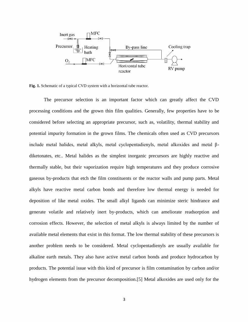
3
Fig. 1. Schematic of a typical CVD system with a horizontal tube reactor.
The precursor selection is an important factor which can greatly affect the CVD
processing conditions and the grown thin film qualities. Generally, few properties have to be
considered before selecting an appropriate precursor, such as, volatility, thermal stability and
potential impurity formation in the grown films. The chemicals often used as CVD precursors
include metal halides, metal alkyls, metal cyclopentadienyls, metal alkoxides and metal β-
diketonates, etc.. Metal halides as the simplest inorganic precursors are highly reactive and
thermally stable, but their vaporization require high temperatures and they produce corrosive
gaseous by-products that etch the film constituents or the reactor walls and pump parts. Metal
alkyls have reactive metal carbon bonds and therefore low thermal energy is needed for
deposition of like metal oxides. The small alkyl ligands can minimize steric hindrance and
generate volatile and relatively inert by-products, which can ameliorate readsorption and
corrosion effects. However, the selection of metal alkyls is always limited by the number of
available metal elements that exist in this format. The low thermal stability of these precursors is
another problem needs to be considered. Metal cyclopentadienyls are usually available for
alkaline earth metals. They also have active metal carbon bonds and produce hydrocarbon by
products. The potential issue with this kind of precursor is film contamination by carbon and/or
hydrogen elements from the precursor decomposition.[5] Metal alkoxides are used only for the

4
growth of thin film oxides due to the highly strong metal oxygen bond. Generally, low
temperature decomposition can generate the desired oxide. Metal β-diketonates also have a
strong metal oxygen bond. The oxidant used is usually ozone instead of oxygen or water vapor.
A marked issue with these precursors is the effect of steric hindrance, which might leave
unoccupied surface sites and decrease the grown film density. Metal alkylamides have relatively
high volatility and active metal nitrogen bonds for reaction with oxidants. It has been found in
certain chemical vapor deposition research that this kind of precursors would show some
'readsorption' behavior and little information is known about the reaction by-products.[5] All the
precursors mentioned above have their own advantages and disadvantages. To make the best
selection, all the precursor properties have to be considered comprehensively. As mentioned
earlier, the selection of precursor is also dependent on the specific type of CVD technique. The
following few paragraphs will introduce the basic classifications.
The CVD technique can be classified into different types due to different standards of
classification. For example, based on the operation pressure, it can be divided into low pressure
CVD (LPCVD), ultrahigh vacuum CVD (UHVCVD) and atmospheric CVD (APCVD). It's
apparent CVD technique can be operated in an environment with a much wider pressure window
than PVD methods, which are often operated under ultrahigh vacuum conditions, for example,
thermal/e-beam evaporation and molecular beam epitaxy. Usually, the lower the system pressure,
the less contamination issues plague thin film growth. However, the decreased pressure is
accompanied with a lower film grow rate. Another way of classification of the CVD technique is
based on different energy types applied to overcome the activation energy barriers of breaking
bonds, such as, thermal CVD, electron beam CVD,[6] laser CVD and plasma enhanced CVD
(PECVD). Among these, PECVD has been extensively studied in the past, especially for thin
5
film growth on thermally sensitive substrates. The reason is that energetic species (electrons,
ions and free radicals) generated in a plasma can activate certain decomposition or surface
reaction processes at a fairly low substrate temperature. Apart from the classical types of CVD
techniques mentioned above, two special types of CVD techniques which are directly related to
the research work of this dissertation is introduced below.
A special type of CVD technique is named atomic layer deposition (ALD). The
difference of ALD from classic CVD is that the exposure of the substrate surface to different
reactive precursors is in a sequential mode and separated from each other by inert gas purging or
vacuum pumping. An essential feature for ALD process is the self saturation behavior of surface
adsorbing species. In this way, the thin film growth can be controlled with atomic accuracy in
terms of thin film thickness and chemical stoichiometry. More details about this technique will
be introduced in 1.1.2.
An important historical concern with CVD is the availability of both volatile and
thermally stable chemical precursors. The development of novel CVD related precursors itself is
always an active area of research for chemists. Another way to conquer this limitation is to
develop high efficiency vaporization system, which can generate high quality vapor phase by
employing the simple chemicals. Classical CVD technique coupled with a vaporization system is
so called direct liquid injection CVD (DLICVD). More information about this technique will be
illustrated in 1.1.3.
As a chemical reaction process, CVD can be carried out in different reactor geometries,
which might affect the pattern of gas fluid flow and thus induce different effects in thin film
growth. The three generic reactor designs are axisymmetric, tube and batch. The axisymmetric

6
one can uniformly deliver precursor species onto the substrate surface. The tube reactor (Fig.1)
has higher processing capacity than the axisymmetric one, but the precursor concentration
decreasing (due to decomposition or deposition) as the gas fluid flows downstream might result
in different thin film growth rates at different tube lengths. The batch reactor has the highest
processing capacity. Since there is usually no bulk convection through the space between wafers,
the mass transfer behavior is always in the form of diffusion. For this reactor, the thin film
growth has to be reaction rate controlled to get uniform deposition, which means the diffusion
rate of gas precursors has to be much faster than the surface reaction rate.[7] It's also noteworthy
that temperature uniformity is essential to get uniform thin films in this mode because the
reaction rate is exponentially dependent on substrate temperature.
Different types of materials including metals, ceramics and semiconductors and materials
with different crystallographic features, such as, polycrystalline, single crystalline and
amorphous can be deposited by CVD technique. Apart from the planar thin film growth, CVD
has also been extensively studied for the growth of 3D nanostructures (nanowires, nanotubes,
etc). CVD has been seen as a standard film growth technique in the semiconductor industry for
manufacturing integrated circuits (IC) components for a long time. Due to the mature
engineering design of CVD equipment, this technique is also now a prevalent tool in other
applications, such as, high speed cutting tools, flat panel displays and photovoltaics.
1.1.2 Atomic Layer Deposition (ALD)
Atomic layer deposition (ALD) as mentioned previously is a chemical vapor deposition
technique based on self-terminating gas solid reactions. A typical ALD process consists of
repeating deposition cycles and each cycle includes four basic steps. These steps are, in sequence,
substrate exposure to gas phase chemical precursor, deposition chamber purging with inert gas or
7
simply evacuating with vacuum pump, substrate exposure to the gas phase oxidant or reductant
chemicals, and the last step of purging the deposition chamber with inert gas. A schematic
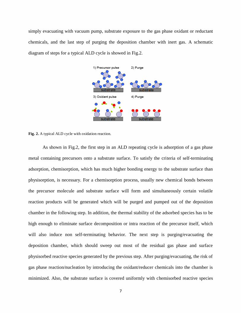
diagram of steps for a typical ALD cycle is showed in Fig.2.
Fig. 2. A typical ALD cycle with oxidation reaction.
As shown in Fig.2, the first step in an ALD repeating cycle is adsorption of a gas phase
metal containing precursors onto a substrate surface. To satisfy the criteria of self-terminating
adsorption, chemisorption, which has much higher bonding energy to the substrate surface than
physisorption, is necessary. For a chemisorption process, usually new chemical bonds between
the precursor molecule and substrate surface will form and simultaneously certain volatile
reaction products will be generated which will be purged and pumped out of the deposition
chamber in the following step. In addition, the thermal stability of the adsorbed species has to be
high enough to eliminate surface decomposition or intra reaction of the precursor itself, which
will also induce non self-terminating behavior. The next step is purging/evacuating the
deposition chamber, which should sweep out most of the residual gas phase and surface
physisorbed reactive species generated by the previous step. After purging/evacuating, the risk of
gas phase reaction/nucleation by introducing the oxidant/reducer chemicals into the chamber is
minimized. Also, the substrate surface is covered uniformly with chemisorbed reactive species
8
for the next reaction step as shown in Fig.2. It has been found that the surface coverage after this
step is usually a fraction of a monolayer, which is due to the effect of steric hindrance of the
ligands and thus certain surface reactive sites will not be covered. The third step is to introduce
oxidant/reducer chemicals into the deposition chamber to react with the active sites of the
previously covered surface. This step is mainly to oxidize or reduce the previously adsorbed
surface by substituting the surface organic ligands with new reactive bonds for the reaction with
precursor molecules of the next cycle. Usually this new formed surface has the same chemical
bonds as the bare substrate surface. The last step is to purge/evacuate the chamber to get rid of
the reactive oxidants/reducers and after this step the substrate is ready to start a new cycle of
deposition.
ALD has few advantages such as digital thickness control at the atomic level, perfect 3D
conformality, large area thickness uniformity, low defect density, possibility of low temperature
deposition (RT~400˚C), and atomically smooth topography. The main disadvantage of the ALD
method is its low growth rate, which is usually less than one atomic layer per cycle. This low
growth rate has limited ALD method mainly to very thin layers deposition, such as the gate
dielectric layer in the MOSFET structure, which is only 2 or 3 nanometers thickness.[8]
1.1.3 Direct Liquid Injection Chemical Vapor Deposition (DLICVD)
CVD technique coupled with various liquid injection/vaporization equipment is usually
defined as direct liquid injection CVD (DLICVD), in which the precursor source is in the state of
liquid solution and injected into the vaporization equipment to generate vapor for the CVD
reaction. By using DLICVD, all the precursors can be prepared as a single source, i.e. dissolving
them (liquid or solid) into an appropriate solvent. After injection into the vaporizer, these
precursors can be vaporized simultaneously and therefore the molar ratio between different
9
precursors would be the same as the corresponding mixing ratio in the solution.[9] Except for
this easy control of element composition, the liquid flow rate can be also controlled simply and
accurately by employing certain liquid mass flow controllers. Compared to the traditional
vaporization techniques, such as bubbler or crucible (for liquid or solid precursors), the mass flux
of precursors entering the CVD chamber is much more reproducible. Another advantage is that
keeping the liquid source at room temperature can minimize the problem of precursor
degradation, which usually happens at elevated temperatures. This method opens up the CVD
process to a larger possibility of precursor chemicals and allows for the deposition of materials
that are very difficult to deposit by conventional vapor transportation. DLICVD has been
successfully applied to the deposition of oxides such as Ba(Sr,Ti)O3, Pb(ZrTi)O3, ZrO2 and
La2O3.[10]
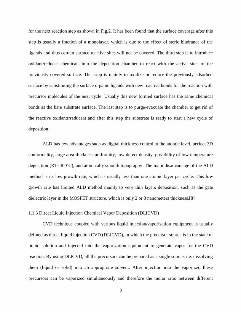
The main goal of vaporizer design is to realize fast, smooth and gentle vaporization.
Usually the liquid precursor is broken into very small droplets (few microns size) first and then
thermally heated by certain hot medium. Either an ultrasonic nozzle or pressurized spraying
technology can be used to break/atomize the injected liquid, which can greatly increase the liquid
surface area and make the vaporization process easier and faster. The thermal heating of the as
generated droplets can be from a hot surface or carrier gas. Generally, the carrier gas, as a
heating medium, can minimize the thermal decomposition effect. A schematic diagram of a DLI
vaporizer using carrier gas as a heating medium is showed in Fig.3 below.

10
Fig. 3. Schematic of a typical direct liquid injection vaporization system.
1.2 Thin Film Growth and Characterization
Thin film growth by chemical vapor deposition is a very complex process including bulk
transportation of gaseous fluid flow, gas phase and surface diffusion, homogeneous and
heterogeneous chemical reaction and film material nucleation. The variation of each of these
processes can to a certain degree result in the change of thin film growth behavior and properties
of the as-grown thin films. The introduction of CVD thin film growth mechanism here will
include most of these physical and chemical processes from the gas phase precursor entering the
reaction chamber to the solid thin film growth on the substrates.
1.2.1 Gas Kinetics
To understand the gas phase kinetic behavior of the precursor molecules in the CVD
chamber, basic concepts of gas kinetics based on statistical mechanics are briefly introduced first.
The statistical distribution of velocities of gas phase molecules at thermal equilibrium has been
well described by the Maxwell-Boltzmann equation:[11]
dN dc
N 4 c2
m
2 kBT 32
exp 1
2mc2
kBT (1.1)
11
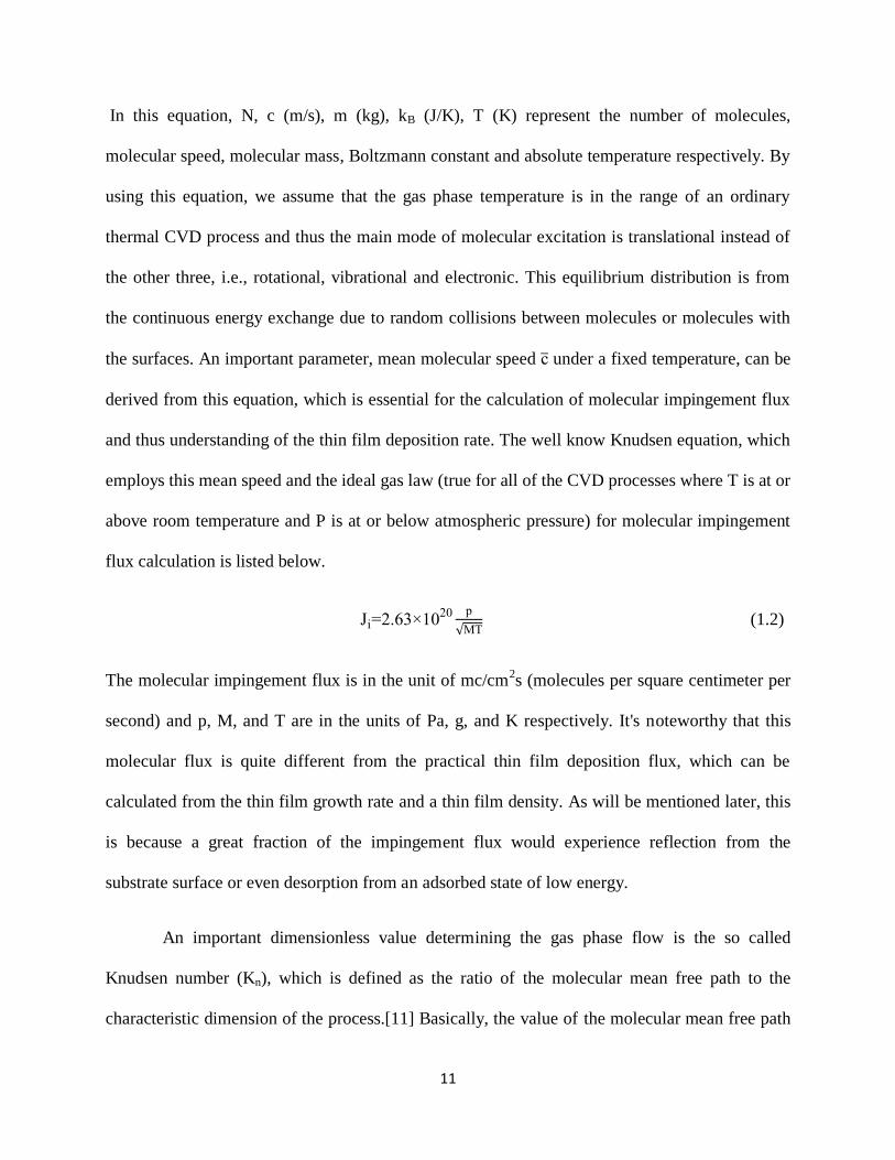
In this equation, N, c (m/s), m (kg), kB (J/K), T (K) represent the number of molecules,
molecular speed, molecular mass, Boltzmann constant and absolute temperature respectively. By
using this equation, we assume that the gas phase temperature is in the range of an ordinary
thermal CVD process and thus the main mode of molecular excitation is translational instead of
the other three, i.e., rotational, vibrational and electronic. This equilibrium distribution is from
the continuous energy exchange due to random collisions between molecules or molecules with
the surfaces. An important parameter, mean molecular speed c under a fixed temperature, can be
derived from this equation, which is essential for the calculation of molecular impingement flux
and thus understanding of the thin film deposition rate. The well know Knudsen equation, which
employs this mean speed and the ideal gas law (true for all of the CVD processes where T is at or
above room temperature and P is at or below atmospheric pressure) for molecular impingement
flux calculation is listed below.
Ji 2.63×10²⁰ p
MT (1.2)
The molecular impingement flux is in the unit of mc/cm2s (molecules per square centimeter per
second) and p, M, and T are in the units of Pa, g, and K respectively. It's noteworthy that this
molecular flux is quite different from the practical thin film deposition flux, which can be
calculated from the thin film growth rate and a thin film density. As will be mentioned later, this
is because a great fraction of the impingement flux would experience reflection from the
substrate surface or even desorption from an adsorbed state of low energy.
An important dimensionless value determining the gas phase flow is the so called
Knudsen number (Kn), which is defined as the ratio of the molecular mean free path to the
characteristic dimension of the process.[11] Basically, the value of the molecular mean free path
12
is predominantly dependent on system pressure unless the temperature is extremely high. The
characteristic dimension, for example, in a CVD process, can be the tube diameter for a tube
reactor. When Kn>1, the process is in high vacuum or molecular flow regime, where the
interactions between molecules are greatly minimized/eliminated. Most physical vapor
deposition methods are operated in this regime to minimize contamination effects. However, the
line-of-sight deposition characteristic makes it difficult to get conformal thin film growth on high
aspect ratio 3D structures. When Kn<0.01, the process is in the viscous fluid flow regime and this
is also the regime of typical CVD processes.
1.2.2 Thin film growth in a CVD process
In a CVD process, convection is the primary way by which bulk gas flow transfer from
the entering shower head to the vicinity of substrate surface. The driving force for this
convection, also known as forced convection, is a pressure gradient. A local convection behavior
due to the buoyancy of gases close to a hot surface is known as free convection, which can often
induce circulating flow patterns and affect the uniformity of as grown thin films. This
phenomenon is mainly related to the reactor shape and gas flow pattern and can thus be
minimized by adjusting certain geometry or gas flow parameters. Generally, the flow pattern
resulting from forced convection can change from laminar flow to turbulent flow and this can be
well determined by the dimensionless Renolds number (Re). Nevertheless, for CVD processes,
due to the normal operation conditions, the flow pattern is nearly always in laminar flow
mode.[11] For such a flow pattern (laminar) in a horizontal tube CVD reactor, the gas velocity
decreases from the tube center to the walls by the force of viscous friction and give rise to a
parabolic velocity distribution. However, more complicated velocity profiles can be induced by
abrupt changes in flow path or by a steep T gradient. When the bulk gas flow across the
13
susceptor, the flow pattern can be distorted to a certain degree at the beginning, but shortly it will
restore to a balanced laminar flow between the susceptor/substrate and the tube wall. This effect
should not affect the thin film growth considering the small influence on the diffusion behavior
in the stationary boundary layer right above the substrate surface. In an axisymmetric CVD
reactor, the flow pattern is more complicated due to the velocity change in both axial and radial
directions when flowing onto the substrate surface. The velocity boundary layer thicknesses are
never going to be much smaller than the susceptor radius under any reasonable flow
conditions.[7]
After the bulk convection delivers the gaseous precursors to the vicinity of the substrate
surface, the convective transport will change to diffusive behavior in a stagnant boundary layer
due to a no-slip boundary condition (velocity at the wall is zero) and viscous friction. The mass
transfer through this layer is driven by the concentration gradient from the bulk gas phase to the
substrate surface where the thin film forming reaction consumes incoming species. The diffusion
kinetics is illustrated by Fick's law, which relates the mass diffusion flux to the concentration
gradient and a diffusivity constant. This diffusivity constant is dependent on certain gas kinetic
parameters introduced earlier, i.e., the mean molecular speed ( ) and mean free path. Considering
the relative kinetics of this diffusion step and the following surface reaction, either of them can
be a rate control step for the thin film growth. A simple model for the understanding of the
control mode is introduced here. Assuming steady-state CVD thin film growth and negligible
desorption/reevaporation, the diffusing species A moving from the bulk gas phase ( nb) to the
growing surface (n0) possesses a diffusivity constant of D and encounters a boundary layer
thickness of δ. According to Fick's law, we can obtain
14
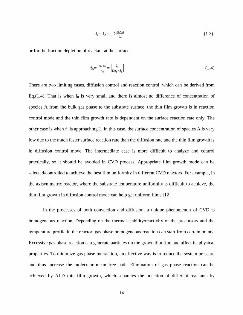
Jr JA -Dnb-n0
δn (1.3)
or for the fraction depletion of reactant at the surface,
f0 nb-n0
nb
Jr
Dnb δn (1.4)
There are two limiting cases, diffusion control and reaction control, which can be derived from
Eq.(1.4). That is when f0 is very small and there is almost no difference of concentration of
species A from the bulk gas phase to the substrate surface, the thin film growth is in reaction
control mode and the thin film growth rate is dependent on the surface reaction rate only. The
other case is when f0 is approaching 1. In this case, the surface concentration of species A is very
low due to the much faster surface reaction rate than the diffusion rate and the thin film growth is
in diffusion control mode. The intermediate case is more difficult to analyze and control
practically, so it should be avoided in CVD process. Appropriate film growth mode can be
selected/controlled to achieve the best film uniformity in different CVD reactors. For example, in
the axisymmetric reactor, where the substrate temperature uniformity is difficult to achieve, the
thin film growth in diffusion control mode can help get uniform films.[12]
In the processes of both convection and diffusion, a unique phenomenon of CVD is
homogeneous reaction. Depending on the thermal stability/reactivity of the precursors and the
temperature profile in the reactor, gas phase homogeneous reaction can start from certain points.
Excessive gas phase reaction can generate particles on the grown thin film and affect its physical
properties. To minimize gas phase interaction, an effective way is to reduce the system pressure
and thus increase the molecular mean free path. Elimination of gas phase reaction can be
achieved by ALD thin film growth, which separates the injection of different reactants by

15
purging the reactor with inert gas. In ALD process, the film forming reactions happens only on
the substrate surface.[13]
The interaction of impinging gas phase molecules with the substrate surface in thin film
deposition is similar to those have been well studied in heterogeneous catalysis. As the
impinging molecules get close to the surface (atomic distance), attractive force due to dipole
interaction between the molecules and the surface bonds can pull the precursor molecules further
onto the surface until a potential well is reached. The as-trapped molecules is in the state of
physisorption and has a relatively weak interaction (Van der Waals force) with the surface. The
fraction of physisorbed molecules in the impinging flux is defined by the trapping probability, δ.
These physisorbed species can either desorb from the surface or move through the surface sites
by surface diffusion. Both of these processes need to surpass certain activation barriers and the
latter process is usually more favorable. The surface diffusion behavior can help the precursors
find each other, find the most active sites, or find epitaxial sites. The physisorbed precursors,
after surface diffusion, can go further to react with the active surface sites by forming new bonds
and/or release certain volatile by-products. These newly formed bonds constitute the basis for
thin film growth. The as-formed surface species is in the state of chemisorption, which has much
stronger bonds than the previous physisorption state. The fraction of chemisorbed molecules in
the impinging flux is defined as chemisorption reaction probability, δ. The chemisorbed species
can also go back to the physisorption state by surface reversal reaction. Due to the desorption
behavior of both physisorption and chemisorption, a more practical parameter called a sticking
coefficient is used to denote the fraction of the arriving vapor that remains adsorbed for the
duration of the experiment. The degree of these surface processes can vary dramatically due to
different surface bonding environments and/or substrate temperatures.[11,14] For example, the

16
surface passivation with certain inert bonds can greatly increase the activation barrier for
chemisorption reaction and thus make thin film deposition difficult.
Nucleation of thin film materials on the substrate surface is driven towards the
minimization of total surface energy, i.e., the sum of the surface energy terms from the as formed
film surface (γf), the interface (γi) and the substrate surface (γs) should be minimized. When the
interfacial bonding is so strong that the resulting small interfacial energy satisfy Eqa. (1.5), the as
(1.5)
grown film material will wet the substrate surface to minimize total surface energy and exhibit
2D layer by layer growth, which is also known as Frank-van der Merwe growth. If the interfacial
bonding is insufficient to hold Eqa. (1.5), the film material will not wet the substrate but instead
form 3D islands, which is known as the Volmer-Weber growth mode. The third growth mode is
Stranski-Krastanov, for which the growth changes from layer to island after a monolayer or two
due to the change in the energy situation with successive monolayer.[11] It's noteworthy that all
of the growth modes above are based on the assumption of sufficient surface diffusion. That is to
say there has to be reasonable surface diffusion rate to get the thermal equilibrium state.
Therefore, it's possible to achieve preferred surface topography by tuning the surface diffusion
kinetics, which is dependent on the substrate temperature. For example, by lowing the substrate
temperature, the island mode growth can be suppressed because of insufficient surface diffusion
to reach the thermodynamic equilibrium and the surface topography can become smoother.
When the substrate temperature is too low to have any surface diffusion behavior, the film
growth is in 'quenched mode', that is the adsorbing species will stay at where they land. For this
case, usually a columnar film structure can be formed and the surface roughness results from
17
statistical roughening. For epitaxy, one more parameter, lattice mismatch is also important for
determining the film growth mode.[15] The lattice mismatch (f) is defined as below,
f af -as as (1.6)
where af and as represent the atomic spacings along some direction in the film and substrate
crystal, respectively. When the thermal expansion coefficients of the two materials are different,
f becomes a function of T and this will also contribute to the temperature dependence of thin film
growth mode or surface topography development.[16,17] For example, at certain high growth
temperatures, due to the difference of thermal expansion, the lattice mismatch becomes large
enough to induce much larger interfacial energy (γi) and thus inequality Eqa. (1.5) will fail and
the thin film growth will change to 3D island mode.
1.2.3 Thin Film Characterization
Thin film characterization includes in situ monitoring of thin film growth behavior and
post deposition measurement of various film properties. The in situ monitoring of thin film
growth can provide continuous updated information such as chemical composition, crystal
structure, surface topography, film thickness, and optical properties, etc.. For instance, reflection
high energy electron diffraction (RHEED) can be used to detect surface crystallographic
information in epitaxy. The RHEED pattern is an instantaneous reflection of the arrangement of
atoms on a thin film surface.[18] Other in situ monitoring tools, such as attenuated total
reflectance Fourier transform infrared spectroscopy (ATR-FTIR), ellipsometry, quartz crystal
microbalance (QCM) are also widely used. Post deposition measurement has a much wider
window of option of analysis techniques. For example, for the chemical composition analysis, X-
ray photoelectron spectroscopy (XPS), Auger electron spectroscopy (AES), Energy dispersive X-
18
ray spectroscopy (EDS), Wavelength dispersive X-ray spectroscopy (WDS), Rutherford
backscattering spectrometry (RBS) can all serve for this purpose. All of these techniques are
nondestructive and can provide both qualitative and quantitative chemical information. For these
techniques, irradiation of the sample with X-ray, electron beam or ion beams are needed to
generate the characteristic signals of each element in the thin film for detection. To differentiate
these techniques, XPS and AES are much more surface sensitive than the others and can give
better quantitative results for small elements such as C, N and O. EDS, WDS, and RBS have
much larger detection depth and usually used for thick films or bulk material analysis. A
common limitation of these techniques is that they cannot detect the smallest elements such as H,
He and/or Li, which might be an important information for certain practical applications.
Secondary ion mass spectrometry (SIMS), another chemical composition analysis technique,
instead can detect all the elements from H to U and it possesses the highest detection limit
compared to other techniques. However, these advantages is compromised by the character of
destructive analysis. Other thin film properties, such as crystal structures can be characterized by
diffraction techniques employing X-ray, electron or neutron beam, surface morphology can be
characterized by Atomic force microscopy (AFM) or Scanning tunneling microscopy (STM) and
magnetic properties can be characterized by Vibrating sample magnetometer (VSM), Alternating
gradient magnetometer (AGM) and Ferromagnetic resonance (FMR). Few representative
techniques, including both in situ monitoring and post deposition characterization, which are
directly related to this dissertation research will be briefly introduced below.
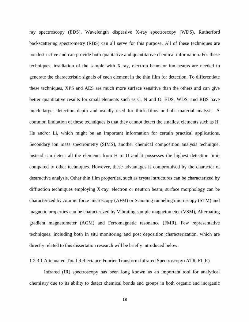
1.2.3.1 Attenuated Total Reflectance Fourier Transform Infrared Spectroscopy (ATR-FTIR)
Infrared (IR) spectroscopy has been long known as an important tool for analytical
chemistry due to its ability to detect chemical bonds and groups in both organic and inorganic

19
samples. The IR absorption behavior is related to the various mechanical vibrational modes in
molecules. A classical vibrational frequency formula for a diatomic molecule containing two
atoms with mass m1 and m2 is illustrated as Eqa.(1.7). In this equation, ν and F represent the
vibrational frequency and the force constant respectively. The number of vibration modes in a
ν 1
2 F
1
m1+
1
m2 (1.7)
molecular system with N atoms is determined by the number of internal degree of freedom,
which means for linear molecules the number of vibration modes is 3N-5 and for nonlinear
molecules the number is 3N-6.[19] Among these vibration modes, usually some of them might
be not IR active and this is determined by the IR selection rule. This rule is that the electric
dipole moment of the molecule must change during vibration in order for a particular vibration
mode to be detected by IR absorption. For example, the 1388 cm-1
symmetric stretch mode for
carbon dioxide gas cannot be detected by IR spectroscopy, while the 2349 cm-1
asymmetric
stretch mode is IR active. A special phenomenon for IR spectroscopy worth to be remembered is
that if a vibration mode of frequency ν is detected then its overtones 2ν, 3ν might also be
detected by IR absorption.[20]
ATR-FTIR is the conjunction of ATR sampling technique into the traditional FTIR
instrument. By doing so, certain samples can be measured more conveniently without complex
sample preparation and moreover it enables the in situ monitoring of certain thin film growth
behavior. For example, the precursor adsorption, reaction with substrate surface and the initial
thin film nucleation can be detected instantaneously without affecting the processing conditions.
ATR technique is based on the principle of total reflection, which happens when the light wave
transmitted from a high refractive index medium into a low refractive index medium and the
20
incidence angle is larger than certain critical angle. For ATR-FTIR, the high refractive index
medium is the optical crystal and the low refractive index medium is the sample, which is in
close proximity to the crystal surface. When the IR light is totally reflected at the internal crystal
surface, a part of this IR wave called the evanescent wave can penetrate through the surface and
interact with the sample at the external surface of the crystal. The penetration depth can be as
deep as a few microns, and is dependent on the frequency of the IR light, the optical properties of
the ATR crystal and the properties of the sample.[21] A schematic of the multiple reflection
ART-FTIR spectroscopy is showed in Fig.4 below.
Fig. 4. Schematic of multiple reflection ART-FTIR spectroscopy.
Different materials can be used as the ATR crystal, such as silicon, germanium, zinc
selenide (ZnSe) and zinc surfide (ZnS). Among these materials, ZnSe has the broadest IR
transmittance window (20000~700 cm-1
), but the hardness and IR useful temperature is low
compared to the others. Silicon is usually the substrate material for microelectronic thin films
deposition. Although the IR transmittance range is narrower (9500~1500 cm-1
), most useful
vibration modes are included in this range, such as C-H, Si-H, O-H, etc.. Therefore, it's a very
useful tool for the surface adsorption and reaction analysis of certain metal organic precursors on
a silicon surface.

21
1.2.3.2 X-ray Photoelectron Spectroscopy (XPS)
XPS is a technique for surface chemical composition analysis. The basic principle is
irradiating the sample surface in vacuum by soft X-rays, such as Mg Kα (1253.6 ev), Al Kα
(1486.6 ev) and monochromatic Al Kα (1486.7 ev), and analyzing the kinetic energies of
generated photoelectrons by a spectrometer. A schematic of the photoelectron generation process
is showed in Fig. 5.
Fig. 5. Schematic of photoelectron generation process.
Based on the energy level of the X-rays used, core level electrons instead of valence
electrons are knocked out of the atomic orbital as shown in Fig.5. The kinetic energy of the as
detected electrons can be an indication of the identity of the element from which the electrons
originate. This is based on the equation of energy conservation during the photoelectric effect,
which is given by:
KE hν-BE-ϕs (1.8)
where hν is the energy of the photon, BE is the binding energy of the atomic orbital from which
the electron originates, and ϕs is the spectrometer work function. Because of the difference in
binding energies for electrons at different atomic orbitals, for each element, there is a unique
XPS energy spectrum. An XPS spectrum is usually plotted in the form of number of electrons
versus the kinetic or binding energy of the as-detected electrons. Besides the sharp peaks
22
representing those characteristic photoelectrons, a continuous background of electrons is also
present in the spectrum. These background signals are mainly from the energy loss electrons due
to inelastic scattering effect when they escape from the sample. Although the as used X-rays can
penetrate as deep as few microns into the sample, the as generated photoelectrons can just travel
through tens of angstroms distance in the material without losing energy. Therefore, the XPS is
very surface sensitive and only chemical information of tens of angstroms beneath the sample
surface can be characterized. Depth profile XPS analysis can be done by using ion gun etching,
but the energetic bombarding ions can also induce chemical changes to the sample surface.
Angle resolved XPS is another way to get information of chemical composition distribution with
depth. Depending on the take-off angle, more signal could be collected either from the surface or
the sublayer.[22] However, the range of probing depth is still limited to the range of tens of
angstroms. Auger lines are often present in the XPS spectra too, which is from the process of
Auger electron ejection that releases the excessive energy in the excited ion left after
photoelectron emission. These lines can also be important for the interpretation of XPS spectra.
The p, d, f levels become split upon ionization, leading to vacancies in the p1/2, p3/2, d3/2, d5/2, f5/2,
and f7/2. The spin-orbit splitting ratio is 1:2 for p levels, 2:3 for d levels and 3:4 for f levels. [23]
Either qualitative or quantitative results could be achieved by XPS analysis. A main issue
for chemical state identification is the charging effect for insulating samples. Surface deficiency
of electrons could make the surface a little positive charged and thus lower the kinetic energy of
the as detected electrons. Usually this charging effect is in a balanced steady state during
measurement and all the peaks in the XPS spectra shift a few electron volts to a higher binding
energy position. Neutralizer (electron flooding) can be used to minimize this charging effect, but
since it's always hard to determine the degree of charging, more flooding electrons could make

23
the surface negative charged. Another way is to shift the peaks based on the adventitious C
(284.8 ev), which is always present on the sample surface after air exposure. For a homogeneous
sample, the number of photoelectrons per second in a specific spectra peak is given by:[22]
I nf θyλAT (1.9)
where n is the number of element per cm3 of the sample, f is the x-ray flux in photons/cm
2-sec,
is the photoelectric cross-section for the atomic orbital of interest in cm2, θ is an angular
efficiency factor for the instrumental arrangement based on the angle between the photon path
and detected electrons, y is the efficiency in the photoelectric process for formation of
photoelectrons of the normal photoelectron energy, λ is the mean free path of the photoelectrons
in the sample, A is the area of the sample from which photoelectrons are detected, and T is the
detection efficiency for electrons emitted from the sample. If we define f θyλAT as the atomic
sensitivity factor, S. The ratio of surface concentration between two elements can be express as
below.
n1
n2
I1 S1
I2 S2 (1.10)
For any spectrometer, it's possible to develop a set of relative values of S for all of the elements.
Multiple sets of values may be necessary for instruments with multiple x-ray sources at different
angles relative to the analyzer. A general expression for determining the atom fraction of any
constituent in a sample, Cx, can be written as:
Cx nx
ni
Ix Sx
Ii Si (1.11)

24
1.2.3.3 X-ray Diffraction (XRD)
X-ray diffraction is a classic technique for crystal structure characterization. X-rays that
can be used to probe the material structures in atomic scale (few angstroms) have wavelengths in
the same order. They usually possess much larger energies than those used for XPS analysis and
are thus called hard X-rays. Generation of these X-rays starts from the bombardment of anode
source materials, such as Cu, Co, Ag, Cr, or Fe etc., with a focused high energy (tens to hundreds
of keV) electron beam. When electrons strike these materials, they are decelerated and a
continuous spectrum of X-ray is emitted known as Bremsstrahlung radiation. High energy
electrons can also knock inner shell electrons out of the atoms and leave vacancies in those shells.
When an outer shell electron falls into the inner shell to fill the vacancy, the excessive energies
left will be relieved by emission of characteristic X-ray photons. The as emitted X-ray possess
the energy (wavelength) characteristic of the shell energy gap of atoms of the source material.
For example, Cu Kα X-ray frequently used in XRD measurement has a wavelength of ~1.5418Å
(~8.04 keV) and Kα here represents the X-ray originating from the action of filling up a vacancy
in K shell by a L shell electron.
nλ 2d sin θ (1.12)
Fig. 6. Geometric derivation of Bragg's law.

25
X-ray diffraction behavior on crystalline materials is vividly described by Bragg's law
(1.12), which clearly illustrates the relationship between X-ray wavelength (λ), lattice parameter
(d) and the diffraction angle (θ). The geometric derivation of Bragg's law is showed in Fig.6. The
difference of path length between the two diffracted X-ray beams determines the interference
situation, e.g., a constructive interference will happen when this difference is an integral number
multiple of the X-ray wavelength. By using this equation, accurate lattice parameters can be
determined by measuring the diffraction angle with a fixed X-ray wavelength. Typical XRD
instruments for thin film analysis have a configuration as showed Fig.7. Usually the incident
beam from the X-ray tube is fixed and the goniometer and detector move in θ(ω) and 2θ angles
and keep in a reflection geometry. The in-plane (ϕ) and out-of-plane tilting angles (ψ) enable the
instrument to do texture and pole figure analysis which can greatly improve understanding of the
crystalline quality, especially for epitaxial thin films.[24]
Fig. 7. Schematic of X-ray diffractometer for thin film crystal structure analysis.
The rocking curve, which is obtained from scanning the angle of ω at a fixed diffraction
angle (2θ), provides valuable information about the out-plane texture of epitaxial films. For non
epitaxial films, more than one lattice plane could be parallel with the thin film surface and

26
exhibit diffraction peaks in the normal θ-2θ scan. The ratio of peaks height is a way to indicate
the degree of growth at preferential orientation. ϕ-scan is a way to characterize the in-plane
texture of epitaxial films, in which a diffraction plane not parallel with the film surface is tilted to
the diffraction position. For example, for films with cubic structure and (001) plane parallel to
the film surface, planes of (101), (011), ( 01), (0 ) can be characterized by ϕ-scan to indicate
the in-plane texture. The as-scanned peak, either from ω-scan or ϕ-scan, provide the texture
information by the peak width, full width at half maximum (FWHM). Generally the narrower the
peak, the better the film epitaxial quality.
Epitaxial films are usually strained as a result of lattice mismatch and/or difference in
thermal expansion coefficient between the film and substrate. For films with cubic structure, the
strain effect could make the structure slightly tetragonal. The calculation of both in-plane (a) and
out-of-plane (c) lattice parameters is thus important to understand this behavior.
sin2θ A h2+k2 +Bl2+C 10sin22θ
1
sinθ+
1
θ (1.13)
For cubic/tetragonal structure, Cohen's method,[25,26] Eqa.(1.13), has been proved to be
accurate and reliable, where θ is the diffraction angle, λ is the X-ray wavelength, and A, B and C
are , and a constant, respectively. By measurements of Bragg angles for various
(hkl) planes, one can determine coefficients A, B and C by least square fitting.
1.2.3.4 Atomic Force Microscopy (AFM)
AFM is tool for nanoscale surface imaging, measuring and manipulating, which was
invented in the early 1980s by scientists from IBM.[27] Different from its precursor, scanning
tunneling microscopy (STM), which requires certain degree of surface conductivity of the
sample, AFM can measure both conductive and insulating materials. AFM has been widely used

27
in thin film surface characterization. The basic working principle of AFM is based on the
distance dependency of interatomic forces. As shown in Fig.8, when a sharp tip is brought into
proximity of the sample surface, the interatomic forces (attractive or repulsive) deflect the tip
attached cantilever up or down. This deflection is detected by a reflected laser beam system and
with the tip raster scanning the surface the instantaneous deflection signal is used by a feedback
loop to tune the vertical position of the cantilever or the sample stage to keep a constant force
(deflection) between the tip and the sample surface. The as generated AFM image illustrates the
surface height profile (topography) for a scanned area of the sample surface.
Fig. 8. Main components of atomic force microscopy system.
AFM can operate in different modes, such as contact mode and tapping mode, to meet the
specific requirements of the sample being measured. Contact mode is also called static mode, in
which the tip is brought so close to the surface and only repelling interatomic forces exist. In this
mode, the potential issue of surface or tip degradation with continuous scanning limits its
application to certain soft samples. Tapping mode, however, can avoid this issue by oscillating
the cantilever in its resonant frequency. The resonance amplitude dependent on the surface
height is usually kept constant for AFM scanning. Based on the tip radius of curvature

28
(nanometers to tens of nanometers), AFM can generate images with resolution of sub nanometer,
which is higher than scanning electron microscopy (SEM) and comparable to transmission
electron microscopy (TEM). Therefore, for very smooth thin film, which has surface RMS
roughness below one nanometer, AFM is a preferred option due to its resolution capability and
much easier sample preparation than TEM. Also, AFM can operate in air or even liquid
environment, which makes it very versatile surface imaging technique. However, AFM has its
own limitations such as the small imaging dimension (tens of microns) and slow imaging speed
(few minutes to take one image).
1.2.3.5 Ferromagnetic Resonance (FMR)
FMR spectroscopy is a technique to probe the magnetization in ferromagnetic (or
ferrimagnetic) materials. Different from nuclear magnetic resonance (NMR), the as-detected
magnetic moments is from the exchange coupled unpaired electrons. Nowadays, it has been
recognized as a standard tool for probing spin waves and spin dynamics.[28]
Fig. 9. Magnetic dipole moment precessing about a static magnetic field.
The FMR phenomenon arises from the precessional motion of magnetization (Fig.9) in a
ferromagnetic/ferrimagnetic material which is in a static magnetic field. Usually the magnetic

29
field is strong enough to saturate the sample. To minimize the system potential energy, the
magnetization will be aligned with the direction of the static magnetic field. When a microwave
field is applied in the plane perpendicular to the static magnetic field. The magnetization will
precess around the equilibrium direction. The classical equation of motion of magnetization (M )
is showed as eqa.(1.14). It's noteworthy that this equation is for an ideal case, where no damping
effect of the precessional motion is considered and this is actually not true for practical
ferromagnetic materials.
dM dt γ M ×H (1.14)
In this equation, γ is the gyromagnetic ratio (2.8 MHz G), H is the total magnetic field applied on
the magnetization including both internal and external fields, such as the static magnetic field,
microwave field and the demagnetizing field. Due to the time varying microwave field
(h ejωt)with frequency ω, there exists a induced time varying magnetization (m ejωt) with the same
frequency. If we neglect the effect of anisotropy, magnetostriction and exchange interaction, the
internal static field is equal to the external applied static field (H 0). When solving the equation of
motion for m , there is a singularity when ω γH 0 and this is the condition of ferromagnetic
resonance based on the assumptions above.[29] For practical ferromagnetic/ferrimagnetic sample,
especially thin film samples, the resonance condition will be different due to various
contributions to the internal magnetic field.
In a typical FMR setup, a resonant cavity and electromagnets are used to exert the
orthogonal static and microwave fields on the sample. The intensity of the microwave signal
after the cavity is detected to determine the absorption behavior. When the precessional
frequency of the sample being measured is equal to the fixed frequency of the resonant cavity the

30
strongest absorption of microwave signal is observed and that is the ferromagnetic resonance
phenomenon. Either the frequency or static magnetic field could be swept to observe the
resonance and get the FMR spectrum. The line width of the as achieved FMR curve is an
indication of the resonance damping behavior, which represents the degree of microwave loss.
Usually narrow line width is preferred for low microwave loss devices. The FMR damping
behavior is sensitive and directly related to many factors of the thin film material such as crystal
defects, chemical inhomogeneity, surface roughness and interface diffusion, etc..[30-32]
Therefore, It's analysis is quite useful for certain thin film device applications.
1.3 Thin Film Application in Electronic and Magnetic Devices
1.3.1 Metal Oxide Field Effect Transistor (MOSFET)
MOSFET is a type of transistor mostly used in integrated circuits (IC) for amplifying or
switching electronic signals. A n-type MOSFET structure is showed in Fig.10. By applying
voltage on the gate electrode, which is separated from the semiconductor body by a thin
insulating oxide layer, an electric field is generated through the oxide layer and affects the
distribution of charged carriers in the interface between the oxide layer and the semiconductor
body. For this n-type MOSFET, the semiconductor body is doped into p type and the source and
drain regions are doped into n type. When a positive voltage is applied on the gate electrode, the
as generated electric field will repel the positive holes away from the layer right below the oxide
and a conducting n-type channel (inversion layer) will be formed between the source and drain.
Therefore, by adjusting the gate voltage, the current through source and drain can be turned on or
off. The onset of strong inversion is defined in terms of a threshold voltage Vth being applied to
the gate electrode relative to the other terminals. In order to assure that the induced inversion
channel extends all the way from source to drain, it is essential that the MOSFET gate structure

31
either overlaps slightly or aligns with the edges of these contacts (self-alignment process). Self-
alignment is preferable since it minimizes the parasitic gate-source and gate-drain
capacitances.[33]
Fig. 10. Schematic of a n-channel MOSFET.
There are three operation modes for practical MOSFET devices. The first one is called
subthreshold mode and it happens when the gate source voltage VGS is lower than Vth. Under this
situation, due to the Boltzmann distribution of electron energies, there are still some high energy
electrons that can flow through the channel and results in a leakage current. This current has
been found exponentially dependent on the value of VGS. When VGS>Vth and the drain-source
VDS voltage is less than the value of VGS-Vth, the MOSFET is in the linear mode. In this mode,
the conducting channel is created for current flow from drain to source and the MOSFET
operates like a resistor. The current is almost linearly dependent on VDS under a fixed gate
voltage. By changing the gate voltage, the resistivity of the conducting channel is changed too.
The third mode is saturation mode when VGS>Vth and VDS>(VGS-Vth). In this mode, the transistor
is in its constant current region and is switched fully on. The onset of this mode is also known as

32
pinch-off to indicate the lack of a channel region near the drain. The drain current is now weakly
dependent upon the drain voltage and controlled primarily by the gate source voltage (VGS).
In the past few decades, the continuous scaling down of the MOSFET in size has
revolutionized the development of the microelectronic industry. The channel length of the
MOSFET structure has been shrinked from microns to tens of nanometers. At this scale, a lot
more functionalities can be realized in a same size wafer and meanwhile the cost of fabrication
can be decreased. However, with this scaling down, few operational problems have been found.
For example, the voltage applied to the gate has to be reduced to maintain reliability. To
maintain performance, the threshold voltage needs to be reduced too. With the reduced Vth, the
transistor cannot be switched from completely off to completely on with the limited voltage
swing available. Subthreshold voltage can thus consume as much as half of the total power
consumption. Another problem is with the gate oxide layer: as the thickness of this layer going
down to few atomic layers, the electron tunneling effect occurs and makes the power
consumption even higher. High-k materials (such as hafnium silicate or oxide) have been
developed to replace the traditional oxide material since the layer can be made thicker while
maintaining the same capacitance.[34-36] To work with these new high-k materials, the
properties of the gate electrode materials have to be considered as well. The traditional gate
electrode material polysilicon, for example, when coupled with a very thin (~1 nm) dielectric
layer, a phenomenon observed is poly depletion, where a depletion layer is formed in the
polysilicon layer next to the dielectric layer when the transistor is in the inversion. To avoid this
problem, metal gate materials such as tantalum carbide, tantalum nitride and titanium nitride can
be used with high-k dielectrics.[37-39]
33
1.3.2 Ferrite-Ferroelectric Layered Heterostructures
Ferrites (spinel, garnet or hexaferrite structure) have been long known as microwave
materials due to their high permeability and resistivity. When used in tunable microwave devices,
such as band-pass filters, phase shifters, or resonators, the microwave propagation behavior in
these materials could be changed by variation of a bias dc magnetic field. This is because of the
change of the permeability of the ferrites resulting from the changing bias magnetic field. This
magnetic tuning is possible over a very wide frequency range, but it is slow and is associated
with large power consumption. Another way of microwave tuning is using ferroelectric materials,
in which electric field can be used to tune the dielectric constant of the materials and thus change
their microwave properties. The tuning by electric field is fast and energy efficient, but usually
the tunable frequency range is very narrow. A combination of ferrite and ferroelectric materials
into composite or layered structures could provide the possibility of simultaneous magnetic and
electric tuning.[40-43] This dual tuning allows the high efficiency of magnetic tuning and the
high speed and low power requirements of electric tuning to be combined. For the work of this
dissertation, only layered structure is introduced here.
Studies on layered ferrite-ferroelectric structures have showed great importance for both
fundamental understanding of high frequency magnetoelectric (ME) effect and various
microwave applications. Two types of layered structures have been investigated. The first one is
ME coupling in bonded bilayers, in which the deformation (strain) of the ferroelectric layer due
to applied electric field results in a magnetic property change of the ferrite layer. Basically, this
strain effect could change the internal magnetic field and thus generate shift of the ferromagnetic
resonance (FMR) field. The degree of coupling depends on both the piezoelectric and
magnetoelastic constants of the ferrite and ferroelectric material being used. The other type of

34
coupling is from unbound ferrite-ferroelectric bilayers, in which hybrid spin-electromagnetic
oscillations and waves are formed.[44,45] Strong ME coupling behavior has been found in both
type of structures.
Fig. 11. ME coupling in a ferrite-ferroelectric layered structure. Reproduced with permission from ref. [46].
The degree of ME coupling effect is usually measured by the shift of FMR resonance
curve. Fig.11 showed the ME effect in a unbound ferrite-ferroelectric bilayer structure.[46] The
as used ferrite material is barium hexaferrite (BaM, BaFe12O19) and the ferroelectric materials is
barium strontium titanate (BSTO, (Ba,Sr)TiO3). At a fixed resonance frequency (60 GHz), a
FMR shift of 6 Oe is observed by applying 29 V voltage to the BSTO layer.
To improve the ME coupling effect, high quality materials are essential for both ferrite
and ferroelectric layers. Different thin film deposition methods have been investigated for the
preparation of either the magnetic or the ferroelectric layer. However, to get both high quality
and relatively thick (few microns to tens of microns) layers is still challenging.

35
CHAPTER 2. LITERATURE REVIEW
Chemical vapor deposition of several electronic/magnetic thin film materials, i.e.,
Hafnium nitride (HfN), Nickel ferrite(NiFe2O4), Lithium ferrite (LiFe5O8), and Barium titanate
(BaTiO3) has been investigated in this dissertation work. All these materials in thin film format
exhibit certain attractive properties and can be promising material candidates for various high
technology devices. In this chapter, a literature review of the physical properties, potential
applications, and various previously reported thin film growth methods for each material is
presented and especially the development of CVD related studies are emphasized.
2.1 Hafnium Nitride (HfN)
2.1.1 Physical Properties and Potential Applications
Hafnium nitride (HfN), a transition metal nitride, has a rock salt structure with lattice
constant of ~4.53Å (Fig.12). It possesses various superior properties, such as, low bulk resistivity
(33µΩ∙cm), high melting point (3380˚C), high hardness and density, low work function (~4.8ev)
and good chemical inertness [47-49]. Because of these excellent properties, HfN can be used as
protective coatings on high speed cutting tools, field emission cathode, and gate electrode and
Fig. 12. Unit cell of HfN crystal with cubic structure.

36
diffusion barrier material in microelectronic devices[50-52], for instance, the potential
application of HfN as a gate electrode material in the metal–oxide–semiconductor field-effect
transistor (MOSFET). It has been well known that the substitution of traditional gate oxide SiO2
with high-k material HfO2 can dramatically accelerate the scaling down of size of MOSFETs.
However, coupling HfO2 with conventional gate electrode layer (poly silicon) will generate
issues like boron penetration and the formation of a low-k interfacial layer, which will affect the
performance of the whole device.[53] HfN can be a good candidate to replace poly silicon to
work with HfO2 as a gate stack due to its excellent properties mentioned above. It has been found
that equivalent oxide thickness (EOT) of HfO2-HfN gate stack can be scaled down to less than 1
nm with excellent leakage and long term reliability even after 1000˚C post metal annealing.
Fig.13 below shows the well behaved electrical characteristics (Id-Vg, Id-Vd) of the n-MOSFET
with an excellent subthreshold slope of 78 mV/dec. The as-used HfN film was deposited by DC
magnetron sputtering of a Hf target in mixed Ar+N2 gas ambient. [52]
Fig. 13. (a) Id-Vg and (b) Id-Vd characteristics of an n-MOSFET using HfN-HfO2 gate stack with EOT 1.18 nm.
Reproduced with permission from ref. [52].
2.1.2 Review of HfN Thin Film Growth
Different methods of HfN thin film deposition have been investigated in the past few
decades. Physical vapor deposition methods such as RF/DC magnetron sputtering [54-58],

37
pulsed laser deposition [59], nitrogen ion implantation [60] and nitrogen ion beam assisted
evaporation [61] have been reported. However, the poor step coverage which comes intrinsically
with PVD methods makes it not appropriate for certain microelectronic applications.
Comparatively, CVD methods have the advantages of larger area deposition, better step coverage
and better control of morphology and stoichiometry over PVD methods. In the development of
CVD deposition of HfN thin films, the introduction of tetrakis (dialkylamido) hafnium (IV)
complexes [62] as hafnium precursors is an important step. The representative precursors and
their vapor pressures are showed in table 1.
Table 1. Hafnium amide precursors and their properties.[63]
Precursor Chemical formula Melting
point (˚C)
Temp
(0.1 torr) (˚C)
Temp (1 torr)
(˚C)
Tetrakis (dimethylamido)
hafnium Hf(N(CH3)2)4 30 48 75
Tetrakis
(ethylmethylamido)
hafnium
Hf(N(CH3)(C2H5))4 liquid 83 113
Tetrakis (diethylamido)
hafnium Hf(N(C2H5)2)4 liquid 96 126
Most of the following studies are based on these metal organic precursors due to their
higher chemical reactivity than hafnium chloride, which needs a very high temperature (>1000˚C)
to react with N2/H2 to form HfN [64]. The CVD reaction of tetrakis (dialkylamido) hafnium (IV)
with ammonia was first studied but resulted in the formation of the insulating phase, Hf3N4,
instead of the conductive phase, HfN [62,65,66]. Highly conformal Hf3N4 films have been
successfully deposited on high aspect ratio surface features, as shown in Fig.14, by ALD method
using tetrakis (dialkylamido) hafnium and ammonia.

38
Fig. 14. A cross sectional scanning electron micrograph of uniform Hf3N4 thin film coating by ALD on a high aspect
ratio trench structure (0.17 μm × 0.3 μm × 7.3 μm). Reproduced with permission from [67].
To improve conductivity of the as deposited thin films, the effect of post rapid thermal
annealing [68] and Ar+ ion milling [69] have been studied. Both of these methods work to a
certain degree by improving the ratio of Hf to N. To satisfy the oxidation state change of
hafnium element from the precursor (+IV) to the product (+III), utilization of a stronger reducing
agent of N,N-dimethylhydrazine (H2NN(CH3)2) has been proposed and studied [70]. In spite of
the formation of relatively pure HfN thin films, the high reaction temperature (600~800˚C) and
the use of a toxic reactant severely limit its application. By employing hydrogen plasma as
reducing agent, two groups have investigated the atomic layer deposition of HfN thin films with
tetrakis (dimethylamido) hafnium (TDMAH) and tetrakis (ethylmethylamido) hafnium (TEMAH)
respectively [71,72]. In these studies, the hafnium precursors played the role of both a Hf and a
N source. It was found that the incorporation of carbon in the phase of hafnium carbide can
improve the thin film conductivity to a certain degree. In our research, a systematic study on both
CVD and ALD methods by using TDMAH and hydrogen plasma will be carried out. Potential
issues and corresponding reaction mechanisms with these methods will be analyzed and
proposed according to our experimental results.

39
2.2 Spinel ferrite: Nickel Ferrite and Lithium Ferrite
2.2.1 Physical Properties and Potential Applications
Nickel ferrite (NiFe2O4) and lithium ferrite (LiFe5O8) belong to the family of
ferrimagnetic ferrites, which possess both high permeability and resistivity.[73] In terms of
crystal structure, NiFe2O4 and LiFe5O8 are both spinel structure. In a spinel (AB2O4) structure,
the unit cell consists of eight formula units and the 8 A2+
and 16 B3+
cations are distributed in the
interstices of the 32 close packed oxygen anions (Fig.15). If all of the 8 A2+
occupy tetrahedral
sites and all of the 16 B3+
occupy octahedral sites then the structure is called normal spinel; If all
of the 8 A2+
and 8 B3+
occupy octahedral sites and 8 B3+
occupy tetrahedral sites, the structure is
called inverse spinel.
Fig. 15. Representation of a spinel structure. Adapted from ref. [73].
Usually, NiFe2O4 and LiFe5O8 both exist in inverse spinel structure at room temperature
and their formulas can be written as Fe3+
[Ni2+
Fe3+
]O4 and Fe3+
[Li+
0.5Fe3+
1.5]O4 respectively.
According to the Néel model, the ferrimagnetism of these ferrite materials comes from a
mechanism of superexchange, in which different magnetic cation occupied sublattices are
antialigned with each other in the presence of an external magnetic field and thus imbalance in
the number of antialigned sublattices results in net magnetism.

40
In spite of the same spinel structure, nickel ferrite and lithium ferrite have their own
crystal parameters and physical properties due to different elements present in the materials.
Nickel ferrite has a lattice constant of 8.340 Å, saturation magnetization of ~3200 G (room
temperature) and Néel temperature of 585 ˚C. The effect of cation distribution and addition of
different divalent cations (Zn2+
, Cu2+
, Mn2+
) on its magnetic properties have been widely
investigated in the past.[74,75] This material is microwave lossy due to the orbital state of Ni2+
, a
relaxing ion. Lithium ferrite exists in two states: ordered and disordered state. In the ordered
phase, the lithium and ferric ions are ordered in a 1:3 molar ratio in the octahedral sites of the
cubic structure. The disordered phase of lithium ferrite has a disordered face centered cubic
structure where the lithium and ferric ions are randomly located in the octahedral interstices. The
disordered phase is produced with quenching from high temperatures as it is formed and
prevalent in the temperature range of 750~1000 ˚C. This is due to the relative diffusion rates of
the ions in the cubic lattice. Slow cooling allows redistribution and ordering of the ions in the
cubic lattice and provides the condition for reversion to ordered phase. The lattice parameters for
the ordered and disordered phase are 8.337 Å and 8.333 Å, respectively. Lithium ferrite has a
saturation magnetization of 3750G (room temperature) and Néel temperature of ~620 ˚C, which
are both higher than that of nickel ferrite. A unique feature of lithium ferrite among those spinel
ferrites is its low microwave loss, which is indicated by its extremely narrow FMR line width of
less than 10 G at room temperature, as showed in Fig.16. It's much lower than the value of nickel
ferrite (40~80G) and comparable to that of yttrium iron garnet (Y3Fe5O8). This is because only S
state Fe3+
ions present in this material. Another advantage of lithium ferrite is its low cost
compared to YIG. However, its practical application is still limited by the challenges of high
quality material preparation, especially for thin films. Also, for microwave applications, both

41
nickel ferrite and lithium ferrite are usually used only in low frequency bands (C or X band) and
external magnets are needed to magnetically bias the material due to their intrinsic small cubic
anisotropy.
Fig. 16. Temperature dependence of FMR line width of bulk lithium ferrite single crystal in ordered phase (FMR
measurement at two frequencies: 12.3 and 19.41 GHz). Reproduced with permission from ref. [76].
Nowadays, the potential application of thin films of these ferrite materials in next
generation technologies, such as monolithic microwave integrated circuits (MMIC) and
multiferroic heterostructures, has made them very attractive.[73,77,78] Considering the
requirements of planar, smaller, weigh less and low loss for these microwave applications, much
research attention has been attracted to the high quality thin film ferrites deposition.
2.2.2 Review of thin film growth methods
Different growth techniques for these ferrite films have been developed and investigated
in the past few decades, such as chemical vapor transport,[79,80] chemical vapor deposition,[81-
87] sputtering,[88-91] liquid phase epitaxy,[92-95] spin-spray plating,[96,97] and pulsed laser
deposition.[98-104] However, the achievement of both high quality (structural, morphological,
magnetic and microwave properties) and thick (1-10 micron range) epitaxial films for microwave
device applications remains challenging.[105,106] For instance, pulsed laser deposition of spinel

42
ferrites has been investigated extensively due to the relative ease of stoichiometry control.[98-
104] Nevertheless, potential issues such as small deposition area and poor thin film conformality
have limited its use mostly to laboratory research. Low growth rate is another bottleneck for
commercially viable device grade spinel ferrites for microwave applications. Liquid phase
epitaxy, which can provide film growth rates as high as tens of microns per hour, is another
promising method that has been widely studied. As a high temperature growth technique,
challenges such as poor surface morphology (hillock growth) and chemical inhomogeneities due
to interdiffusion between substrate and thin film, which can greatly influence thin film magnetic
properties, are still unresolved (Fig.17). [107,93]
Fig. 17. FMR measurement (9.07 GHz, perpendicular) of lithium ferrite film grown by LPE method on
Mg(In,Ga)2O4 (111) substrate. Presence of inhomogeneity in the film is indicated by the complex FMR curve.
Reproduced with permission from ref. [93].
The use of CVD for nickel ferrite film deposition has been limited by the availability of
appropriate metal precursors having both high volatility and thermal stability. Early work
(~1960s) investigated the use of solid metal halide precursors. But the high temperature (>700˚C)
required to vaporize these precursors and the formation of corrosive hydrogen halides hampered
further development.[81,82] More volatile metal acetylacetonate precursors for nickel ferrite
deposition, (Ni(acac)2 and Fe(acac)3), have been utilized in subsequent studies.[108,109]
Der
ivat
ive
of
pow
er a
bso
rpti
on
8600 8700 8800 8900
Applied magnetic filed (Oe)

43
However, using traditional vaporization methods (bubbler or crucible), accurate control of vapor
concentrations for the two components in order to obtain stoichiometric films is difficult, often
resulting in unwanted impurity phases such as Fe2O3 or NiO.[108] Precursor oligormerization
(e.g., [Ni(acac)2]3) and weak thermal stability above 200˚C are two additional drawbacks of this
approach.[109] To the best of our knowledge, no research has been reported for lithium ferrite
thin film deposition by using CVD technique with any metal organic precursors so far.
Fig. 18. Schematic diagram of a previous reported DLI-CVD system for nickel ferrite growth. Reproduced with
permission from ref. [83].
The direct liquid injection (DLI) technique, which can generate vapor from a liquid
solution source at relatively low temperatures (< 200°C), has in recent years been successfully
utilized for a number of metal-organic chemical vapor deposition processes.[110-112] DLI-CVD
is a particularly useful method for multi-component systems as several precursors can be
dissolved in the same solution and the relative delivery rates of precursors are defined by the
solution composition. There are only a couple of reports in the literature on DLI-CVD of nickel
ferrite, e.g., using metal thd (thd = 2,2,6,6-tetramethyl-3,5-heptanedionato) precursors.[83,85] In
spite of reported polycrystalline/epitaxial growth of nickel ferrite on different substrates (Si(100)
and MgO(100)), the as-deposited thin film characteristics (morphology and magnetic properties)
are far from satisfactory as compared to bulk nickel ferrite. One of the DLI-CVD experimental

44
systems is showed in Fig.18.[83] As one can see, the simple syringe injection and hot plate flash
vaporization has potential issues such as poor control of liquid injection rate and thermal
decomposition of metal organic precursors by direct contact with the hot metallic surface. The
properties of the films are greatly influenced by the specific vaporization procedure, the selection
of metal organic precursors, solvent and substrate material, and especially processing conditions
(temperature, pressure, etc.). In this dissertation, we report the epitaxial growth of both nickel
ferrite and lithium ferrite films on various substrates by DLI-CVD using a commercial
vaporization technique. Optimization of the DLI parameters, thin film growth mechanism,
relationship between CVD processing conditions and thin film qualities will be investigated.
2.3 Barium Titanate (BaTiO3)
2.3.1 Physical Properties and Potential Applications
Barium titanate (BaTiO3) has a classical perovskite crystal structure with formula of
ABO3, in which A and B represent cations of different size. In the structure of barium titanate,
the larger Ba2+
cations and O2-
anions form a face-centered cubic (FCC) lattice and the smaller
Ti4+
cation occupies the octahedral site (cubic center). Unit cell of perovskite barium titanate is
shown in Fig.19. Barium titanate is a piezoelectric material. Above its curie temperature of
120˚C, barium titanate exists in cubic phase and shows paraelectric effect. While below 120˚C
(>5˚C), it transits to tetragonal phase (a 3.992Å, c 4.032Å at 20˚C) resulting from a tiny
distortion of the Ti4+
included octahedron. The coupling of these distorted octahedra in the
crystal gives rise to large spontaneous polarization and thus barium titanate exhibits ferroelectric
characteristic.[113]

45
Fig. 19. Unit cell of perovskite BaTiO3 crystal.
Due to its ferroelectric property and high dielectric constant, barium titanate has been
recognized as a very useful material for certain cutting edge technologies, such as thin film
capacitors, magnetoelectric heterostructures, and non-volatile ferroelectric random access
memory (FeRAM) devices.[114] Besides, the desirable nonlinear optical properties of BaTiO3
make it attractive for a variety of electro-optic and optical storage device applications.[115]
2.3.2 Review of thin film growth methods
Thin film deposition of BaTiO3 has been investigated using different methods, such as
RF sputtering,[116-119] evaporation,[120,121] pulsed laser deposition,[122-125] molecular
beam epitaxy,[126] sol-gel[127] and chemical vapor deposition.[128-140] The achievement of
single crystal, high quality, and good surface morphology has always been the goal for most
deposition methods in order to fulfill the requirement of practical devices. Epitaxial growth of
BaTiO3 thin films has been found in both physical and chemical vapor deposition methods on
different substrates, such as MgO,[117,122,130,135,136,138] TiO2,[123] SrTiO3,[116,136]
LaAlO3,[115,131,136] and NdGaO3.[131] Chemical vapor deposition, as mentioned previously,
has several advantages over physical vapor deposition. Studies on CVD of BaTiO3 thin films
have been reported since early 1990s. Its development has been based on the progress of
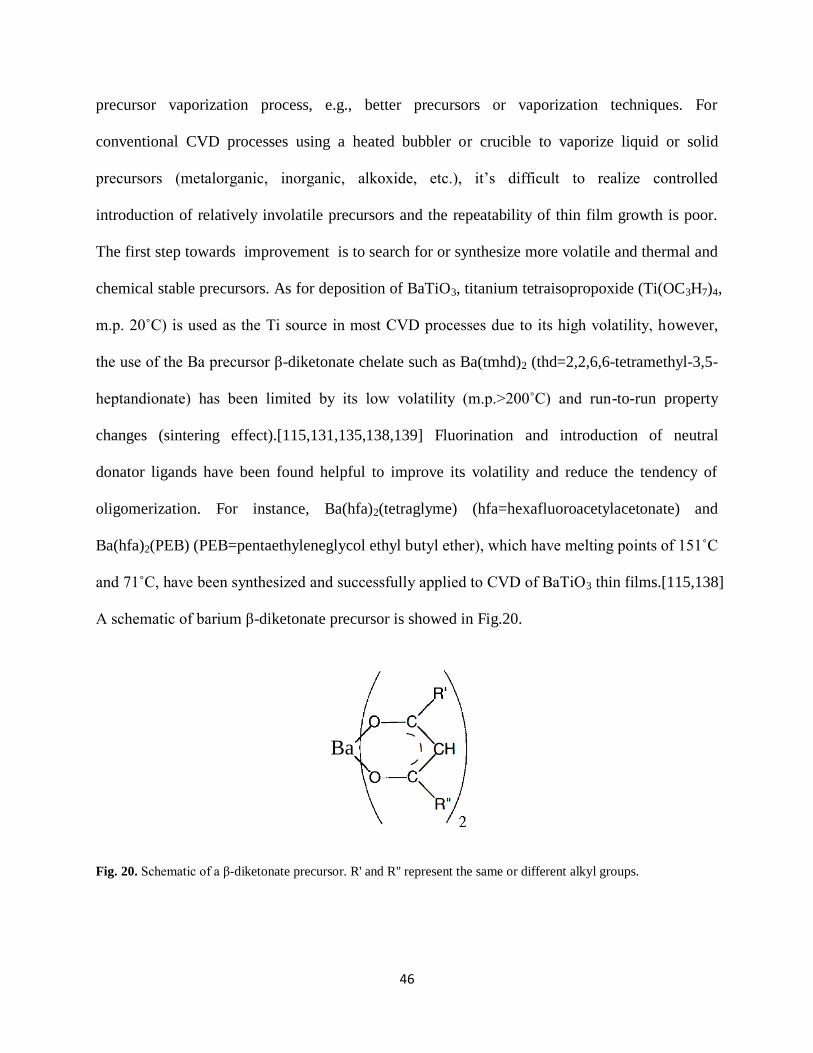
46
precursor vaporization process, e.g., better precursors or vaporization techniques. For
conventional CVD processes using a heated bubbler or crucible to vaporize liquid or solid
precursors (metalorganic, inorganic, alkoxide, etc.), it’s difficult to realize controlled
introduction of relatively involatile precursors and the repeatability of thin film growth is poor.
The first step towards improvement is to search for or synthesize more volatile and thermal and
chemical stable precursors. As for deposition of BaTiO3, titanium tetraisopropoxide (Ti(OC3H7)4,
m.p. 20˚C) is used as the Ti source in most CVD processes due to its high volatility, however,
the use of the Ba precursor β-diketonate chelate such as Ba(tmhd)2 (thd=2,2,6,6-tetramethyl-3,5-
heptandionate) has been limited by its low volatility (m.p.>200˚C) and run-to-run property
changes (sintering effect).[115,131,135,138,139] Fluorination and introduction of neutral
donator ligands have been found helpful to improve its volatility and reduce the tendency of
oligomerization. For instance, Ba(hfa)2(tetraglyme) (hfa=hexafluoroacetylacetonate) and
Ba(hfa)2(PEB) (PEB=pentaethyleneglycol ethyl butyl ether), which have melting points of 151˚C
and 71˚C, have been synthesized and successfully applied to CVD of BaTiO3 thin films.[115,138]
A schematic of barium β-diketonate precursor is showed in Fig.20.
Fig. 20. Schematic of a β-diketonate precursor. R' and R'' represent the same or different alkyl groups.
Ba
47
Another way to break through the limitation of vaporization is the technique of direct
liquid injection, in which the precursor containing the liquid source is injected into a vaporizer
and is volatilized there before it’s delivered into the CVD reactor by a carrier gas. In this way,
the vaporization temperature can be dramatically decreased and the introduction of precursor can
be accurately controlled by a sensitive liquid flow meter. A couple of studies have been reported
based on this technique in CVD of BaTiO3 or (Ba,Sr)TiO3 thin films.[114,136,141] The reported
results show that this can be a very promising technique for the deposition of high quality and
thick BaTiO3 films. Considering the desirability of thick (tens of microns) and high quality
ferroelectric films in the study of magnetoelectric coupling effects in layered
heterostructures,[142] our research on CVD of BaTiO3 films will take advantage of the direct
liquid injection technique.

48
CHAPTER 3. PLASMA ENHANCED ATOMIC LAYER DEPOSITION OF HAFNIUM
NITRIDE FILMS
3.1 Introduction
Chemical vapor deposition of HfN can make films of high conformality and thus provide
the possibility of fabricating high aspect ratio microelectronic structures. One of the challenges
for this method is the selection of appropriate chemicals. Hafnium amide precursors have been
successfully used in the deposition of HfO2, Hf3N4 and HfN by reacting with oxygen (O2),
ammonia (NH3) and dimethyl hydrazine (H2NN(CH3)2) respectively.[63,67,70] For the
deposition of HfN using dimethyl hydrazine, usually a high substrate temperature (600˚C~800˚C)
is needed to initiate the reaction, which is not appropriate for certain thermal sensitive materials
used in the microelectronic devices. Hydrogen plasma which has much higher reactivity than
hydrazine can be used in low temperature plasma enhanced ALD process of HfN thin
films.[71,72] In this chapter, the hafnium precursor tetrakis (dimethylamido) hafnium (IV)
(TDMAH) used for thin film growth is studied first, i.e., in-situ monitoring of adsorption and
reaction behavior of TDMAH on hydrogenated Si(100) by ATR-FTIR. It's important to
understand the thermal decomposition and surface adsorption behavior of this precursor for ALD
thin film growth, because it is directly related to the film contamination and interfacial bonding
information.[143] PEALD of HfN thin film growth by using TDMAH and hydrogen plasma is
studied. The as-deposited thin films were characterized by XPS, AFM, XRD, SEM and TEM to
study the chemical composition, surface morphology and crystal structure information. Thin film

49
resistivity was measured by four point probe and its dependency on plasma power has been
investigated.
3.2 Tetrakis (Dimethylamido) Hafnium (IV) (TDMAH) Adsorption and Reaction on
Hydrogenated Si(100) Surface
3.2.1 Introduction
TDMAH is in the form of colorless to pale yellow crystal at room temperature, which has
a melting point of around 30˚C and a vapor pressure of around 0.1 torr at 48˚C. This material is
moisture sensitive and should be handled in low temperature and/or inert environment. Its
molecular structure is showed in Fig.21.
Fig. 21. Molecular structure of TDMAH.
One of the important concerns for ALD precursors is their thermal stability. If the
precursors decompose in the process of transporting to the substrate surface or on the substrate
surface, it's likely to induce continuous thin film growth and break the rule of self-terminating
adsorption. It's noteworthy that the kinetics of thermal decomposition also has to be considered,
if the degree of decomposition is negligible in the ALD cycle time range, it should not be a big
issue to affect the thin film growth.[8] Another concern for the ALD precursors is the surface
reactivity, i.e., the activation barrier for interfacial bond formation between the precursor and the
surface dangling bonds has to be low enough to allow film growth. In-situ ATR-FTIR is one
efficient way to achieve all of these information through monitoring the surface adsorption and
reaction behavior of precursor molecules. TDMAH has been widely used in ALD of HfO2, but

50
the initial surface chemistry for thin film growth is rarely investigated.[144] In this section, the
temperature dependence of TDMAH adsorption, desorption and thermal decomposition on
hydrogenated Si(100) surface is studied. Besides, Density Functional Theory (DFT) is used to
calculate the IR spectrum of intact TDMAH molecule to help interpret the experimental IR
results.
3.2.2 Experimental Details
The in-situ ATR-FTIR experimental setup is showed in Fig.22. The TDMAH (99%)
precursor was bought from STREM Chemicals and used without any further purification. Before
the in-situ ATR-FTIR experiment, the TDMAH in liquid phase was characterized by a 'liquid
drop' experiment, in which the TDMAH precursor was directly loaded onto the crystal surface
and measured by ATR-FTIR. For the TDMAH adsorption experiment TDMAH was loaded into
a quartz tube bubbler. All the loading processes were in a nitrogen purged glove bag to minimize
reaction/contamination with oxygen or water vapor.
Fig. 22. Experimental setup of the in-situ ATR-FTIR.
51
In a typical in-situ ATR-FTIR experiment, the bubbler with loaded TDMAH was kept in
an oil bath at 60˚C. Around 20 min of stabilization is needed before introduction of the gas phase
precursor into the ATR cell. No carrier gas was used in the experiments. The ATR cell, as shown
in the bottom of Fig.22, uses a trapezoidal shaped crystal for enhanced surface sensitivity via
multiple internal reflections of the IR beam along the long parallel faces of the crystal. The front
face of the crystal is exposed to the precursor, while the IR beam enters and exits from the
angled faces of the crystal from below. In the experiment, Si (100) crystals (Ge or ZnSe crystal
for liquid drop experiment) with 45 degree bevels were mounted in a custom built flow through
cell. With a crystal size of 50×10×2mm, the incident IR beam internally reflects 13 times off the
TDMAH-adsorbed face before it reaches the DTGS (deuterated triglycine sulfate) detector
(within NicoletTM
4700 FTIR device). The sealing of the ATR cell uses a custom made Kalrez
gasket between the cell frame and the crystal surface edges. The cell was roughly pumped
(Rotary vane pump, Edwards RV3F) to a base pressure of about 5 mtorr. The crystal temperature
could be controlled up to 250 ºC, with the limitation from excited Si phonon modes resulting in
reduced transparency of the crystal. Before each experiment, the gas delivering lines and the
ATR cell were heated to around 100˚C and purged with ultra high purity N2 for 1 hour to
minimize the water vapor concentration in the system. Once the valve between the bubbler and
the ATR cell was opened, TDMAH started flowing into the ATR cell, the computer controlled
IR spectra taking was simultaneously started. In this flowing mode, the surface adsorption and
reaction behavior were instantaneously monitored. All the IR data were taken in the IR range of
400~4000 cm-1
and averaged over 16 scans with a resolution of 4 cm-1
, which took 22 seconds
for each spectrum. The IR spectra taking was preset into an automatic mode, in which the FTIR
will take one spectrum by one spectrum until the preset number (30) of spectra was reached. A

52
delay time of 2 seconds between spectrum taking was also set. The TDMAH adsorption was
monitored in the flowing mode (valve open) for the time range of 15 IR spectra (~6 min). After
that, the bubbler valve was closed, when the ATR cell was still under pumping, the automatic IR
spectra taking was still running one by one to monitor the surface desorption/reaction process
until the preset number of spectra is reached. The first 15 spectra taken in the flowing mode are
used to simulate the precursor pulse step in an practical ALD cycle, and the second 15 spectra in
the pumping mode were used to simulate the purging step in an ALD cycle. These ATR-FTIR
experiments were carried out under different crystal temperatures from room temperature to
250˚C. In each experiment, a spectrum of the bare crystal was taken before the TDMAH vapor
was introduced into the ATR cell and used for background subtraction.
The as used Si(100) ATR crystal was prepared to hydrogenated silicon surface by the
procedures below:
1. Sequentially ultra sonication by organic solvents acetone and methanol (2 min each).
2. Rinse with DI water for 2 min.
3. Cleaning with a 1:1:5 solution of NH4OH+H2O2+DI H2O at 80˚C for 10 min to remove the
organic contaminants.
4. Soaking in diluted BOE (buffered oxide etch, NH4F:HF = 10:1, BOE:DI water = 1:5) for 20 s
to remove the oxide layer.
5. Cleaning with a 1:1:6 solution of HCl+H2O2+DI H2O at 80˚C for 10 min to remove metallic
(ionic) contaminants.
6. Repeat step 4.
7. Rinse with DI water for 10 min.

53
8. Blowing dry with ultra high purity N2.
TDMAH molecular modeling and bond dissociation energy (BDE) calculation were
carried out by Density Functional Theory (DFT) coupled in Gaussian 03 software. The
calculations were performed at the DFT level with the hybrid gradient-corrected B3LYP
exchange-correlation functional. The geometry optimizations and frequency calculations were
done with the 6-31+G(d,p) basis set for the first row atoms and the LanL2DZ relativistic
effective core potential (RECP) basis set for the Hf atom, All energies were corrected with the
zero point energies (ZPE). The software and computing resources are from Alabama
Supercomputer Authority.
3.2.3 Results and Discussion
The TDMAH precursor was first characterized by ATR-FTIR in a 'liquid drop'
experiment. Few drops of liquid TDMAH were loaded onto a Ge(100) ATR crystal in a nitrogen
glove bag and the IR spectrum was taken under room temperature. The as taken IR spectrum is
showed in Fig.23 (bottom). Since Ge (100) ATR crystal has a wider IR transmittance window
than Si(100) at room temperature, vibrational modes as low as 700 cm-1
can be observed. The top
spectrum is from DFT molecular modeling of a TDMAH free molecule. The molecular structure
of TDMAH is fully optimized before the frequency calculation. As one can see, the experimental
and theoretical results match very well in spite of a small shift of the peak positions. One
possible reason is that the experimental measurement is for the liquid phase TDMAH and the
inter molecular interaction could thus influence the electronic structure of the molecules. All the
peaks have been identified by considering the theoretical results and certain previous
experimental IR studies on transition metal amides.[145,146] Bond dissociation energies of Hf-N
and N-C bonds in the TDMAH molecule have been calculated to be 78.4 Kcal/mol and 69.7

54
Kcal/mol respectively. The stronger Hf-N bond makes it thermodynamically possible for the
deposition of HfN without any extra N source.
Fig. 23. Experimental and theoretical modeled IR spectrum of TDMAH.
In-situ monitoring of TDMAH adsorption on hydrogenated Si(100) surface is carried out
at different substrate temperatures. Fig.24 shows the IR spectra after 2 min TDMAH adsorption
at different crystal temperatures in the flowing mode.
Fig. 24. IR spectra of TDMAH adsorption on hydrogenated Si(100) at different temperatures.

55
The spectrum taken at room temperature is the same as that observed in the liquid drop
experiment, which indicates the physisorption and homogeneous condensation behavior of
TDMAH at room temperature. With increasing substrate temperature, apparent changes
happened both in the C-H stretching region and the ~1600 cm-1
region. The decreasing peak
intensity of 2770 cm-1
, which represents one of the C-H stretching modes that influenced by the
lone pair electrons on N, indicates bond dissociation in the intact TDMAH molecules.[147] The
peaks at 1591 cm-1
and 1639 cm-1
starts at 100˚C and becomes much stronger at 150˚C should be
attributed to bonds in certain TDMAH decomposition products. Based on certain IR research on
transition metal amides (Ti, Zr, V, Nb), we tentatively assign the peaks to Hf-H and N=C
stretching modes, which come from the decomposition mechanism of β-hydride
elimination(Eq.(3.1)).[148] It's obvious that the decomposition of surface adsorbed TDMAH on
hydrogenated Si(100) starts at temperatures between 100 to 150˚C in our measurement time
range.
(3.1)
The adsorption and desorption behavior of TDMAH on hydrogenated Si(100) surface
were also analyzed quantitatively. The change of integrated area of C-H stretching modes
(2700~3000 cm-1
) with time is showed in Fig.25. For both adsorption and desorption period, at
different substrate temperatures, the change of C-H stretching intensity with time shows different
profile. At 100˚C, most TDMAH molecules are intact in the experimental time range (6 min) and
the adsorption is in physisorption regime, where the molecules are trapped on the surface by
weak Van der Waals force. This weak adsorption is indicated by the fast desorption (large

56
negative slope) behavior in the pumping mode Fig.25 (b). Noteworthy, in the adsorption mode,
the curve doesn't saturate even after 6 min, which should be explained by the multilayer
physisorption behavior. Adsorption at 150˚C shows even sharper increase of C-H stretching
signal. As seen in Fig.24, the strong decomposition signals observed at 150˚C indicated presence
of great amounts of decomposition products, which also include certain alkyl groups. Therefore,
the sharp increasing behavior should be contributed to the accumulation of both intact TDMAH
and thermal decomposition products. As one can see for the desorption profile of 150˚C
experiment, its desorption rate is much slower than that at 100˚C. This might be because of the
Fig. 25. Integrated C-H stretching area change with TDMAH (a) adsorption and (b) desorption time at different
substrate temperatures.
57
slow kinetics of the desorption of the decomposition products from the surface. For practical
ALD experiments at this temperature, long purging/pumping time is necessary to remove these
species to minimize thin film contamination. At high temperatures (200˚C and 250˚C), the
increased desorption rate of certain decomposition products with increasing temperature makes
the adsorption behavior close to self-termination with a slight increasing trend. However, the
self-terminating C-H containing adsorbates might result from a balance of TDMAH adsorption
and decomposition products desorption rates and cannot represent a self-terminating thin film
growth.
As mentioned earlier, the peak of 2770 cm-1
has been recognized as an indication of the
existence of intact TDMAH molecules on the surface. This C-H stretching mode has a frequency
much lower than the normal C-H stretching modes found in alkyl groups and is usually observed
in transition metal alkyl amides. The ratio of this peak to the whole C-H stretching region is
monitored in the adsorption/desorption period and showed in Fig.26. As one can see in this
figure, in the adsorption mode, left region of the vertical blue line, the ratio of peak 2770 cm-1
is
decreasing with increasing adsorption temperature, which indicates more TDMAH
decomposition at higher deposition temperatures. In the desorption region, right of the vertical
blue line, the as adsorbed species can keep in the same chemical format for certain time range
and this time range is decreasing with increasing temperature, which can be explained by
increased decomposition kinetics at higher temperatures. The long tail of the 150 ˚C desorption
behavior might be attributed to the existence of large amounts of adsorbed TDMAH
decomposition products. Interesting phenomenon has been observed for the 100 ˚C desorption,
as showed in Fig.26, the desorption was composed of two steps (flat regions), which indicates

58
the existence of both physisorbed and small amount of chemisorbed TDMAH molecules on the
surface.
Fig. 26. Change of ratio of peak 2770 cm-1
to the whole C-H stretching area in the period of adsorption and
desorption at different substrate temperatures.
The profile of Si-H bonds changing on the ATR silicon crystal surface in the period of
TDMAH adsorption and desorption at different crystal temperatures is showed in Fig.27. As one
can see, at 100˚C, there is almost no change of surface Si-H bonds in the adsorption and
desorption process. Starting from 150˚C, the introduction of TDMAH induced apparent
subtraction of surface Si-H bonds and after stopping TDMAH flow the surface Si-H bonds kept
in a stable level. Sufficient thermal energy is achieved above 150˚C for the reaction between
TDMAH and Si-H bonds to happen. The stable Si-H bonds after TDMAH introduction indicates
that the thermal energy itself can not break these bonds. The reaction of surface Si-H bonds with
the thermally activated (or decomposed) TDMAH molecules is the main way for surface bonds
subtraction.[149]
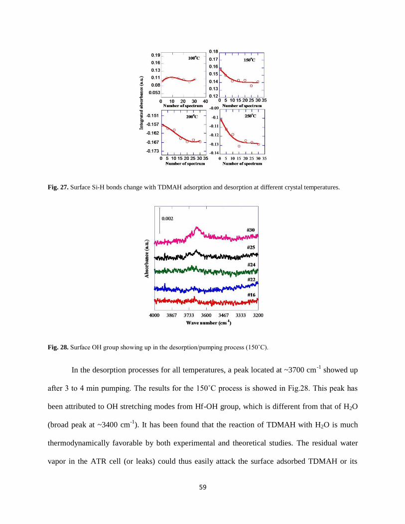
59
Fig. 27. Surface Si-H bonds change with TDMAH adsorption and desorption at different crystal temperatures.
Fig. 28. Surface OH group showing up in the desorption pumping process (150˚C).
In the desorption processes for all temperatures, a peak located at ~3700 cm-1
showed up
after 3 to 4 min pumping. The results for the 150˚C process is showed in Fig.28. This peak has
been attributed to OH stretching modes from Hf-OH group, which is different from that of H2O
(broad peak at ~3400 cm-1
). It has been found that the reaction of TDMAH with H2O is much
thermodynamically favorable by both experimental and theoretical studies. The residual water
vapor in the ATR cell (or leaks) could thus easily attack the surface adsorbed TDMAH or its

60
decomposition products (Hf-H) and generate Hf-OH groups on the surface. This might not be a
big effect in the deposition of HfO2, but it will disastrous and definitely contaminate the
deposition of Hf3N4 or HfN films.
3.3 Plasma Enhanced Atomic Layer Deposition of HfN Films
3.3.1 Introduction
HfN thin film has showed excellent properties for being used as the gate electrode
material to work with HfO2 (gate dielectric layer) in the MOSFET structure. PEALD of high
quality HfN thin film at low substrate temperatures would be an greatly preferred process for
practical fabrication. Previous studies on PEALD of HfN by using hafnium amides and hydrogen
plasma has reported the incorporation of C elements in the as deposited thin films. However, the
related thin film growth chemistry is rarely investigated. In this dissertation research, aside from
the surface chemistry study of TDMAH precursor by ATR-FTIR, in-vacuo XPS is also used to
study the as grown thin film surface. These work can provide a clear picture of the HfN thin film
growth chemistry and its relation to thin film physical properties.
3.3.2 Experimental Details
Hafnium nitride (HfN) thin film deposition on hydrogen terminated Si(100) and
thermally grown SiO2 (on Si) substrates was carried out in a home built plasma enhanced atomic
layer deposition (PEALD) system (Fig.29). This PEALD chamber is a part of a ALD/CVD thin
film deposition cluster and connected to a in vacuo XPS system by vacuum gate valves, as
showed in Fig.30.

61
Fig. 29. Schematic of the plasma enhanced atomic layer deposition system.
Fig. 30. ALD/CVD thin film deposition cluster coupled with in vacuo X-ray photoelectron spectroscopy.
Tetrakis (dimethylamido) hafnium (Hf(N(CH3)2)4, 99% ) purchased from STREM
Chemicals Inc. was used as the metal organic precursor without any further purification. The n-
type Si(100) wafer with native oxide was cleaned by standard RCA procedure and then dipped
into a diluted BOE (NH4F:HF=10:1) solution for 20 s to remove the surface oxide and passivate
the surface with Si-H bonds. Then the Si wafer was rinsed by DI water for 10 min and blowing

62
dried by ultra high purity N2 gas. The as prepared hydrogen terminated Si(100) wafer was loaded
into the reaction chamber for thin film deposition or underwent further thermal oxidation in a
tube furnace (Lindberg) to form a SiO2 layer with thickness of 100 nm to 120 nm. In a typical
PEALD reaction, the bubbler filled with TDMAH was heated to 60˚C by an oil bath heater and
the TDMAH delivery line from the bubbler to the reaction chamber was heated to around 75˚C
to minimize precursor vapor condensation on the tubing walls. Hydrogen gas is introduced into
the reaction chamber by passing through a quartz tube where it is ionized into hydrogen plasma.
As shown in Fig.29, the quartz tube is wrapped by a copper solenoid, which is connected to the
RF power generator (coupled with matching network). In our case, 13.56 MHz RF power is used
to generate inductively coupled plasma (ICP) in the quartz tube. Since the generation of plasma
is out of the reaction zone, the effect of substrate surface bombardment by powerful ions can be
minimized. The introduction of TDMAH and hydrogen plasma was separated by flowing inert
gas (Ar) between them. A typical ALD cycle is composed of the following four sequential steps:
5s TDMAH vapor, 35s Ar purging, 25s hydrogen plasma, 5s Ar purging. The pulsing of the
reactants and inert gas and the pulsing of the plasma are synchronized in a self written LabVIEW
program (Fig.31). Through serial communication (RS232/RS485) with a PC, the RF power
generator and a programmable relay controlling all the pneumatically controlled valves can be
controlled simultaneously by this LabVIEW program. In this way, the plasma was turned on
exactly at the time range of hydrogen pulse through the quartz tube, as shown in Fig.32.

63
Fig. 31. LabVIEW program for the control of PEALD process.
Fig. 32. Synchronized reactants and plasma pulsing sequence in PEALD experiments.
The reaction chamber is coated with Si3N4 (PECVD using He diluted SiH4 and N2 plasma)
to minimize the effect of out gassing. The base pressure of the reaction chamber is pumped to
around 5×10⁻⁸
torr by a turbo molecular pump (Pfeiffer). In the deposition process, the chamber
is pumped by a rotary vane vacuum pump (Leybold) and the system pressure is automatically
controlled by a MKS throttle valve.
The as deposited thin films were characterized by an in vacuo XPS system (APEX,
Physical Electronics Inc.), which was connected to the deposition chamber through a gate valve,
as showed in Fig.30. The vacuum pressure of sample transfer path is below 10-7
torr. The

64
pressure for XPS analysis is around 5×10⁻⁹
torr. The as used X-ray is Mg Kα (1253.6 eV) with a
power of 100W (15kV). The sample analysis area is 6×6 mm2. The pass energy of the electron
spectrometer is set to 100 eV for survey spectra and 25 eV for high resolution spectra. Depth
profile analysis was also carried out in this XPS system by using a 5kV Ar+ ion gun and the
etching area was set to the same as the analysis area. A nominal etching rate of 1 nm/min is
achieved under our experimental conditions. The thin film cross section were characterized by
field emission scanning electron microscopy (JEOL 7000) and transmission electron microscopy
(TECNAI F20). The FESEM was operated at accelerating voltage of 20 kV with a spot size of 8
and working distance of 10 mm. High resolution TEM picture of the thin film interface was
taken under field emission gun voltage of 200 kV. Zone axis of [100] was taken for the single
crystal Si substrate. Thin film surface topography was studied by atomic force microscopy
(Nanoscope IV, Digital Instruments). The AFM was operated in tapping mode using AFM tips of
NSC15/AIBS (MikroMasch) with tip radius of curvature of around ~10 nm, force constant of
~40 N/m and resonance frequency of ~325 kHz. Crystallographic information was studied by X-
ray diffractometer (X’pert, Philips) and thin film thickness by X-ray reflectivity. The thin film
sheet resistance was measured by a four point probe.
3.3.3 Results and Discussion
Incorporation of oxygen has been found in the PEALD deposited thin films in spite of the
low system base pressure (~10-8
torr), chamber wall coating with Si3N4 and the pre-sputtering of
substrate with hydrogen plasma. Considering the small air contamination effect for an in-vacuo
XPS analysis, the oxygen has been attributed to the residual oxidants (H2O/O2) in the deposition
ambient which can react with TDMAH and be buried into the film. One factor has been found to
affect the degree of oxygen incorporation is the inert gas purging time after TDMAH pulse. By
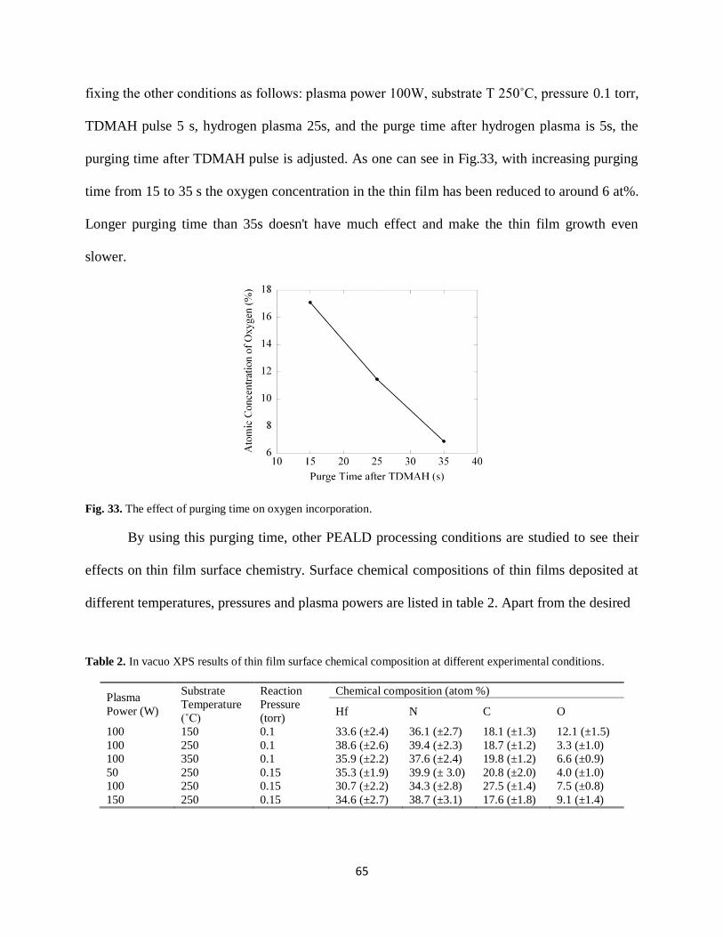
65
fixing the other conditions as follows: plasma power 100W, substrate T 250˚C, pressure 0.1 torr,
TDMAH pulse 5 s, hydrogen plasma 25s, and the purge time after hydrogen plasma is 5s, the
purging time after TDMAH pulse is adjusted. As one can see in Fig.33, with increasing purging
time from 15 to 35 s the oxygen concentration in the thin film has been reduced to around 6 at%.
Longer purging time than 35s doesn't have much effect and make the thin film growth even
slower.
Fig. 33. The effect of purging time on oxygen incorporation.
By using this purging time, other PEALD processing conditions are studied to see their
effects on thin film surface chemistry. Surface chemical compositions of thin films deposited at
different temperatures, pressures and plasma powers are listed in table 2. Apart from the desired
Table 2. In vacuo XPS results of thin film surface chemical composition at different experimental conditions.
Plasma
Power (W)
Substrate
Temperature
(˚C)
Reaction
Pressure
(torr)
Chemical composition (atom %)
Hf N C O
100 150 0.1 33.6 (±2.4) 36.1 (±2.7) 18.1 (±1.3) 12.1 (±1.5)
100 250 0.1 38.6 (±2.6) 39.4 (±2.3) 18.7 (±1.2) 3.3 (±1.0)
100 350 0.1 35.9 (±2.2) 37.6 (±2.4) 19.8 (±1.2) 6.6 (±0.9)
50 250 0.15 35.3 (±1.9) 39.9 (± 3.0) 20.8 (±2.0) 4.0 (±1.0)
100 250 0.15 30.7 (±2.2) 34.3 (±2.8) 27.5 (±1.4) 7.5 (±0.8)
150 250 0.15 34.6 (±2.7) 38.7 (±3.1) 17.6 (±1.8) 9.1 (±1.4)

66
Hf and N elements, incorporation of C and O on the thin film surface is also found. Similar
results have been reported by other groups, which were attributed to contamination from sample
air exposure.[71,72] This explanation is apparently unconvincing considering that the same
phenomena happened in our in-vacuo XPS analysis. To better understand the chemistry
happening in the ALD process, an XPS depth profile analysis was carried out using a 5kV Ar+
ion gun. The XPS spectra and quantitative chemical composition changing with etching depth
are shown in Fig.34 and table 3, respectively.
Fig. 34. XPS depth profile analysis of (a) Hf4f (b) N1s and (c) C1s in an as deposited HfNxCy thin film. Sample
prepared at 250˚C, 0.15 torr, 100W.

67
Table 3. Chemical composition change with depth of analysis.
Atomic concentration (at%)
Hf N C O
Surface 30.0 35.8 25.7 8.4
Intermediate 36.5 36.5 19.2 7.9
Bulk 49.3 31.7 14.3 4.6
In the spectra and table above, ‘surface’ means XPS analysis without any etching,
‘intermediate’ represents a very thin layer (2~3nm) measured immediately after surface etching
and before the constant bulk properties, and ‘bulk’ means most of the thin film thickness where
no (or very small) qualitative or quantitative chemical changes can be detected. Fig.34(c) shows
a large C 1s peak from thin film surface analysis, which indicates more than 20 at% C. The
position of this C 1s peak is at 286.1 ev, which is different from the C 1s signal of adventitious
hydrocarbon (284.8ev). This result further rules out the possibility of air contamination. This
carbon signal probably comes from the N-C bonds, which exist in complexes of TDMAH
incomplete decomposition products. This assignment was supported by the existence of the left
shoulder on N 1s peak in Fig.34(b), which represents N in an organic matrix. With Ar+ ion
etching, the chemical state change of C 1s peak shows a clear trend from organic carbon (N-C,
286.1ev) to metal carbide (Hf-C, 282.3ev). Meanwhile, the peak shoulder on N 1s disappeared
gradually. Although the existence of hafnium carbide phase was reported as a natural phase
produced by PEALD reaction in the bulk, the possibility of chemical state change due to ion
sputtering could not be ruled out. Apart from the disappearance of N-C groups due to ion etching,
another obvious change is the shape and position of Hf 4f peak. The height ratio between the two
spin orbit splitting peaks of Hf 4f5/2 and Hf4f7/2 increases with sputtering time until the bulk
properties are obtained. It has been reported in certain XPS studies of hafnium nitride thin film
that Hf4f5/2 has relatively stronger intensity than Hf4f7/2 due to the enhancement effect of N 2s.
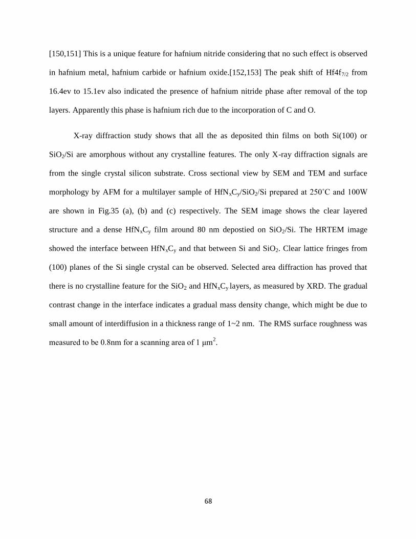
68
[150,151] This is a unique feature for hafnium nitride considering that no such effect is observed
in hafnium metal, hafnium carbide or hafnium oxide.[152,153] The peak shift of Hf4f7/2 from
16.4ev to 15.1ev also indicated the presence of hafnium nitride phase after removal of the top
layers. Apparently this phase is hafnium rich due to the incorporation of C and O.
X-ray diffraction study shows that all the as deposited thin films on both Si(100) or
SiO2/Si are amorphous without any crystalline features. The only X-ray diffraction signals are
from the single crystal silicon substrate. Cross sectional view by SEM and TEM and surface
morphology by AFM for a multilayer sample of HfNxCy/SiO2 Si prepared at 250˚C and 100W
are shown in Fig.35 (a), (b) and (c) respectively. The SEM image shows the clear layered
structure and a dense HfNxCy film around 80 nm depostied on SiO2/Si. The HRTEM image
showed the interface between HfNxCy and that between Si and SiO2. Clear lattice fringes from
(100) planes of the Si single crystal can be observed. Selected area diffraction has proved that
there is no crystalline feature for the SiO2 and HfNxCy layers, as measured by XRD. The gradual
contrast change in the interface indicates a gradual mass density change, which might be due to
small amount of interdiffusion in a thickness range of 1~2 nm. The RMS surface roughness was
measured to be 0.8nm for a scanning area of 1 μm2.

69
Fig. 35. (a)Cross sectional view of HfNxCy on SiO2/Si (b)HRTEM images of the HfNxCy-SiO2 and SiO2-Si
interfaces (c) surface topography by AFM, RMS roughness is 0.8nm.
Fig. 36. X-ray reflectivity measurement of the as deposited HfNxCy films at different plasma powers. The ALD
cycles of deposition are 200, 200, and 300 for 50W, 100W, and 150W, respectively.
X-ray reflectivity (XRR) results of the as deposited thin films under different plasma
powers are showed in Fig.36. The thin film thickness is fitted by using the Philips WinGixa
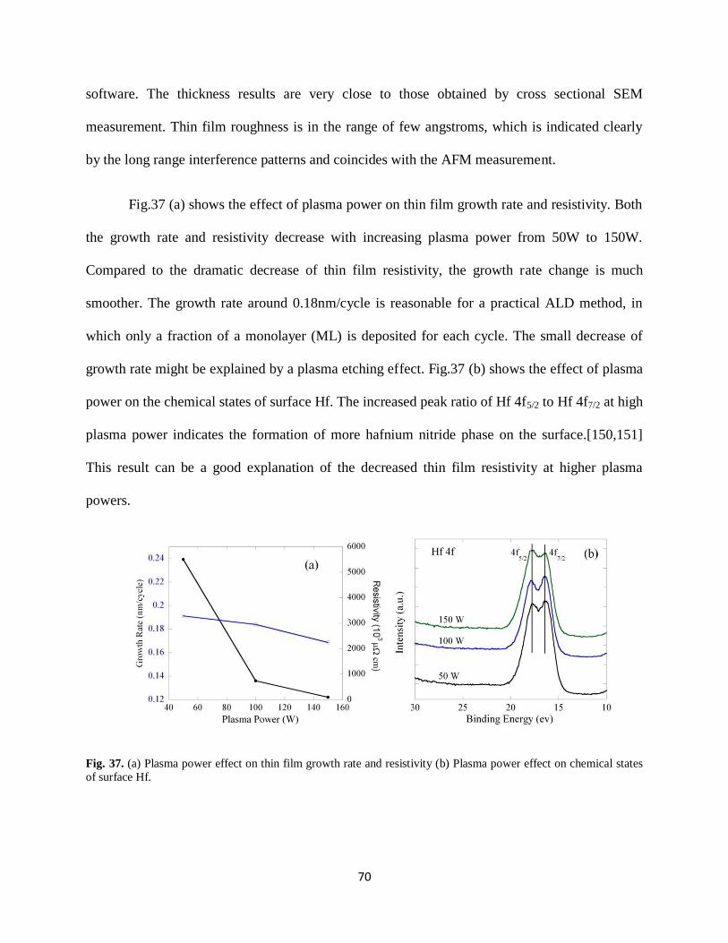
70
software. The thickness results are very close to those obtained by cross sectional SEM
measurement. Thin film roughness is in the range of few angstroms, which is indicated clearly
by the long range interference patterns and coincides with the AFM measurement.
Fig.37 (a) shows the effect of plasma power on thin film growth rate and resistivity. Both
the growth rate and resistivity decrease with increasing plasma power from 50W to 150W.
Compared to the dramatic decrease of thin film resistivity, the growth rate change is much
smoother. The growth rate around 0.18nm/cycle is reasonable for a practical ALD method, in
which only a fraction of a monolayer (ML) is deposited for each cycle. The small decrease of
growth rate might be explained by a plasma etching effect. Fig.37 (b) shows the effect of plasma
power on the chemical states of surface Hf. The increased peak ratio of Hf 4f5/2 to Hf 4f7/2 at high
plasma power indicates the formation of more hafnium nitride phase on the surface.[150,151]
This result can be a good explanation of the decreased thin film resistivity at higher plasma
powers.
Fig. 37. (a) Plasma power effect on thin film growth rate and resistivity (b) Plasma power effect on chemical states
of surface Hf.
71
3.4 Conclusion
In summary, TDMAH adsorption and reaction on hydrogenated Si(100) surface has been
investigated by in-situ ATR-FTIR experiments. It has been found that for temperatures below
100˚C, physisorption is the main mode of TDMAH adsorb onto the crystal surface and no
obvious surface Si-H bonds breaking. These physisorbed TDMAH molecules can be pumped
away easily. At temperatures between 100˚C and 150˚C, surface adsorbed TDMAH molecules
start to decompose and newly emerging IR peaks at 1591 cm-1
and 1639 cm-1
were assigned to
N=C and Hf-H vibrational mode respectively based on a β-hydride elimination mechanism. The
decomposition species on the surface has been found hard to desorb at low temperatures, which
can contaminate the thin film growth if the purging/pumping time is not long enough. The
surface Si-H bonds subtraction has been found for adsorption above 150˚C and it's closely
related to the TDMAH decomposition behavior.
Hafnium nitride thin film deposition by PEALD using TDMAH and hydrogen plasma has
been investigated. Uniform and moderately conductive HfNxCy thin films were deposited on
Si(100) and SiO2 substrates. A thin surface layer (2~3nm) containing both hafnium nitride and
organic complexes of TDMAH decomposition has been found by in vacuo XPS analysis. Depth
profile analysis by XPS indicated the existence of hafnium carbide phase in the bulk. Thin film
resistivity is greatly affected by the level of hydrogen plasma power, in which higher plasma
power results in lower thin film resistivity. In spite of this tunability of resistivity by plasma
power, carbon incorporation is still a big issue for this PEALD method. Therefore, more
appropriate reducing agent or nitrogen source is probably needed to get pure HfN thin film by
CVD/ALD method.

72
CHAPTER 4. DIRECT LIQUID INJECTION CHEMICAL VAPOR DEPOSITION OF
FERRIMAGNETIC NICKEL FERRITE AND LITHIUM FERRITE FILMS
4.1 Introduction
Nickel ferrite (NiFe2O4) and lithium ferrite (LiFe5O8) thin film growth by DLI-CVD
technique is reported in this chapter. The achievement of both high quality and thick spinel
ferrite thin film materials is particularly essential for the fundamental research of ME
(magnetoelectric) effect in ferrite-ferroelectric bi-layer structures and practical application in
dual tunable microwave devices.[40,41] DLI-CVD technique has the potential capability of
fulfilling these requirements. To achieve these objectives, the main research work includes
material selection (precursor, solvent, and substrate), processing condition optimization
(vaporization and CVD process) and thin film characterization (structural, morphological, and
magnetic properties). More results have been obtained for nickel ferrite thin film deposition.
Effect of the CVD growth conditions on the thin film physical properties is studied. Possible
reaction mechanisms and thin film growth modes have been proposed upon experimental results.
Single crystal quality and thin film defects are characterized by various techniques, including
XRD, polarized Raman and TEM. Great emphasis is focused on FMR properties of the as grown
nickel ferrite films, which directly related to its microwave applications. Nickel ferrite thin film
growth on various piezoelectric substrates are also investigated. For the lithium ferrite thin film
growth, certain preliminary results have been obtained.

73
4.2 DLI-CVD Growth of NiFe2O4 Films
Nickel ferrite (NiFe2O4) is a well known insulating and high permeability magnetic
material that is commonly used in transformer cores and microwave applications.[73] It
possesses a spinel (Fd 3 m) structure (a = 0.834 nm) with the tetrahedral A sites occupied by half
of the Fe3+
cations, whereas the remaining Fe3+
and Ni2+
cations are distributed over the
octahedral B sites (Fig.15). Recently, much attention has been attracted to the growth of epitaxial
spinel ferrite thin films for magnetoelectric applications and monolithic microwave integrated
circuits (MMIC).[43,77] For instance, the magnetoelectric effect in magnetic/ferroelectric
heterostructures is promising for tunable microwave devices, such as filters and phase shifters,
offering much faster tuning response and lower power consumption.[46]
As mentioned in chapter 2, a wide variety of thin film growth techniques have been
developed and investigated in the past for nickel ferrite (and with divalent cation substitutions).
However, the achievement of both high quality (structural, morphological, magnetic and
microwave properties) and thick (1-10 micron range) epitaxial films for microwave device
applications remains challenging.[73,78] Chemical Vapor Deposition (CVD) offers a number of
advantages over other deposition methods, but its use for nickel ferrite film deposition has been
limited by the low volatility and thermal stability of available chemical precursors. The direct
liquid injection (DLI) technique, which can generate vapor from a liquid solution source at
relatively low temperatures, has in recent years been successfully utilized for a number of metal-
organic chemical vapor deposition processes.[110-112] DLI-CVD is a particularly useful method
for multi-component systems as several precursors can be dissolved in the same solution and the
relative delivery rates of precursors are defined by the solution composition. Thin film growth
rate can be extremely high due to the possible high rate of precursor introduction into the thin

74
film growth region. The properties of the films are greatly influenced by the specific
vaporization procedure, the selection of metal organic precursors, solvent and substrate material,
and especially processing conditions (temperature, pressure, etc.). In this chapter, we report the
epitaxial growth of relatively thick nickel ferrite films on various substrates using the DLI-CVD
technique.
Various challenges for epitaxial growth of complex magnetic oxides (e.g., ferrites) by
CVD methods are to be expected. The first consideration is the reactivity of metal organic
precursors, which has to be optimal for decomposition and film growth on the substrate surface
but avoid gas phase reactions/nucleation. Moreover, the decomposition temperature ranges of the
individual precursors should be sufficiently close to help retain the cation ratio of the solution
source in the thin film. For growth on a lattice-matched substrate, the temperature has to be
sufficiently high to provide adequate surface diffusion of the adsorbing species for epitaxial film
growth and yet maintain a smooth surface morphology.
In this work, anhydrous Ni(acac)2 and Fe(acac)3 (acac is an abbreviation for
acetylacetonate) in the molar ratio of 1:2 are dissolved in N, N-dimethyl formamide (DMF) to
form the precursor solution. DMF acts as a solvent and can simultaneously minimize
intermolecular association by coordinating with the metal ions.[154,155] A Brooks Instrument
DLI 200 Vaporizer system is used, which vaporizes the liquids using a heated inert gas instead of
a hot metallic surface. This approach enables more gentle vaporization of the solution source
with minimal thermal decomposition of the precursors. MgAl2O4 (100) and MgO (100)
substrates with cubic normal spinel (a = 0.808 nm) and fcc (2a = 0.842 nm) structure,
respectively, are used for systematic study of film growth due to their close lattice match with
nickel ferrite (lattice mismatch of 3% and 1%, respectively).[81,101,102] Deposition on other

75
substrates such as MgO(111), and piezoelectric SrTiO3(100), PMN-PT (Pb(Mg1/3Nb2/3)O3-
PbTiO3) (100), and PZN-PT (Pb(Zn1/3Nb2/3)O3-PbTiO3) (100) is also investigated under certain
experimental conditions.
4.2.1 Experimental Details
Nickel ferrite films are deposited on MgAl2O4 (100) and MgO (100) substrates in a
horizontal 1.5 inch diameter quartz tube furnace. The DLI-CVD experimental set-up is shown in
Fig.38.
Fig. 38. Experimental set-up of DLI-CVD system for the growth of nickel ferrite films.
As shown in Fig.38, The CVD reactor is a three zone low pressure quartz tube furnace.
The tube reactor, with a diameter of 1.5 in. and length of 50 in., was pumped down to the
reaction pressure (12 Torr) by a rotary vane vacuum pump (Leybold, Trivac). Ni (acac)2 (98%)
and Fe(acac)3 (99%), bought from Sigma-Aldrich, were used as metal organic precursors without
any further purification. These precursors were dissolved in N, N-dimethyl formamide (DMF) in
a molar ratio of 1:2 as the source for liquid injection. Ultrahigh purity He (20 psi) was used to
pressurize the liquid flow from solution container to the vaporizer. The flow rate of the liquid
76
solution was accurately controlled by a Brooks Quantim liquid MFC (10 g/h, full range)
connected to the DLI200 vaporizer system. Ultrahigh purity argon gas was used as the carrier gas,
which served both as the vaporization medium and the delivery gas. The liquid vaporization
process is accelerated by a sequential input of mechanical and thermal energy. At the vaporizer
inlet, where the liquid and carrier gas flow intersect, is an atomizer, which breaks up the entering
fluid into fine droplets (2~5μm) because of a large pressure drop. Efficient heat and mass
transport between the fine droplets and the preheated carrier gas (Ar) results in the metal-organic
precursors being homogenously entrained in the solvent vapor and carried into the reactor
without premature decomposition. Ultrahigh purity oxygen was used as the oxidant. Atomically
polished single crystals such as MgAl2O4 (100) and MgO (100) of dimensions
5mm×5mm×0.5mm from CrysTec Gmbh were used as substrates. Before loading into the reactor,
the substrates were ultrasonically cleaned sequentially in acetone and isopropanol and then blow
dried with N2. The vaporizer system was cleaned with pure DMF solvent after each run. Typical
processing conditions are summarized in Table 4.
Table 4. Typical processing conditions for DLI CVD of epitaxial NiFe2O4 films.
Substrate MgAl2O4 (100) / MgO (100)
Reaction pressure (Torr) 12
Growth temperature (˚C) 500-800
Concentration of solution (Fe(acac)3, mol/L) 0.067
Solution flow rate (g/hr) 6
Ar carrier gas flow rate (sccm) 300
Vaporizer temperature (˚C) 175
Oxygen flow rate (sccm) 300
Prior to investigation of the CVD process conditions, we optimized the vaporizer
operation parameters (including precursor solution injection rate, carrier gas (Argon) flow rate,
vaporizer temperature, inlet and outlet pressures) by inspecting the surface morphology and

77
chemical composition of nickel ferrite film grown at 600˚C. As a starting point, we chose the
vaporizer temperature based on the thermal properties of the solvent and precursors (b.p. of DMF
153˚C, m.p. of Ni(acac)2 230˚C, m.p. of Fe(acac)3 184˚C). Other physical properties of the
solvent (e.g., density, viscosity and heat of vaporization) are also important in choosing the
carrier gas and liquid flow rates, and vaporizer pressure. All the vaporizer parameters have to be
tuned for optimal flow of the precursors into the CVD reactor without decomposition. Deviations
from the optimized parameters, such as in the vaporizer temperature or liquid flow rate, results in
a rough film surface and/or changes in stoichiometry from the desired composition. This can be
attributed to an inadequate vaporization process due to precursor(s) decomposition, condensation
on tubing walls, or the presence of insufficiently vaporized droplets/clusters. In this paper, if not
specified, all the vaporizer operations are fixed at these optimized values (Table 4).
The film morphology was characterized by both FE-SEM (JEOL-7000) and AFM (Vecco
Nanoscope-IV). The JEOL-7000 FE-SEM system was also equipped with an EDX (Oxford
Instruments) measurement system for chemical composition analysis. For the FE-SEM and EDX
characterization, operating conditions were as follows: accelerating voltage 20 KV, beam spot
size 8, and working distance 10 mm. All the samples were attached to the sample holder by
carbon tape and no metallic coatings on the sample surfaces were deposited. For the AFM
characterization, ultra sharp non-contact silicon cantilevers (MikroMasch, NSC15/AIBS) with a
typical probe tip radius of ~10nm and resonant frequency of ~325 kHz were used in tapping
mode. Transmission electron microscopy was used to characterize the crystal structure and
defects. XRD (Philips X’pert Pro) was used to investigate crystallographic properties of the as-
deposited films. Cu Kα radiation was used as the X-ray source. All the samples were
characterized under similar experimental conditions (with a nickel filter and 0.5˚ divergence slit

78
size). For the rocking curve analysis, 2θ was fixed at the NiFe2O4 (400) diffraction angle while
scanning ω. The Raman spectra of NiFe2O4 single crystal and NiFe2O4/MAO films were
measured under nominally identical conditions using a T64000 (Jobin Yvon) spectrometer
equipped with a microscope and a liquid nitrogen cooled CCD detector. The 633 nm laser line of
a He-Ne laser was used for excitation. The magnetic properties were studied using an AGM
(PMC, Micromag-2900) system with a magnetic field scan to 16 kOe. The four edges and
backside of each sample were polished by sandpaper before the AGM measurements.
4.2.2 Results and Discussion
4.2.2.1 Thin Film Growth on MgAl2O4 (100) and MgO (100)
4.2.2.1.1 Oxygen Effect on Film Morphology
Fig. 39. The effect of oxygen flow rate on thin film surface morphology observed using field emission scanning
electron microscopy. (a) Without oxygen flow, film of porous structure is formed; (b) particulates formation under
high oxygen flow rate.
Unlike typical CVD reactions where metal-organic precursors are the only reactant
species, DLI-CVD involves the combustion of a large concentration of organic solvent vapor. In
our case, the consumption of oxygen by DMF (flash point 58˚C) has to be considered. To
investigate the effect of oxygen flow on the thin film growth, we carried out two control

79
experiments at a deposition temperature of 700˚C on both MgAl2O4 (100) and MgO (100)
substrates. The first experiment involves film growth without any oxygen flow (just the argon
carrier gas). Film growth by thermal decomposition of the metal chelate precursors occurs in the
absence of oxygen.[108] However, as can be seen from the SEM micrograph image in Fig.39 (a),
the as-deposited film shows a very porous structure. EDX (Energy Dispersive X-ray
Spectroscopy) analysis reveals the presence of a significant excess of Fe than in stoichiometric
nickel ferrite, along with trace amounts of carbon (< 2%). The porous structure is likely related
to incomplete decomposition together with the slow kinetics of the surface reaction and/or
desorption of the by-products. Based on thermal stability studies of the precursors, the
preferential incorporation of iron may be attributed to the lower thermal stability of Fe(acac)3
than Ni(acac)2.[156-158] The effect of high oxygen flow rate, double of what is needed for
growth of smooth and stoichiometric films (Table 4), is studied in the second control experiment.
As shown in Fig.39(b), a relatively smooth and dense film is obtained. The correct chemical
composition (Ni:Fe = 1:2) is obtained under this condition. However, small particles (10-100 nm
range) are observed on the film surface. The particulate formation can be attributed to gas phase
nucleation, which is a common and undesirable feature in CVD reactions, especially at high
reaction pressures. Particulates buried in the film during growth can result in crystalline defects
and thus influence the physical properties. It is noteworthy that the film growth rate does not
increase with the increased oxygen flow rate. Comparing the results of these two experiments,
the oxygen flow influences the thin film growth kinetics and helps balance the deposition rates of
Ni and Fe. It is likely that more of lower molecular weight volatile products, such as CO2, are
generated in the presence of oxygen and thus minimize the problem of blocked surface
adsorption sites. Based on mass spectrometry studies Igumenov et al. [159] suggest that the

80
oxygen does not participate in the formation of the oxide phase during thermal decomposition of
metal β-deketonates. Instead, its role is primarily to oxidize the organic fragments to form
smaller molecular weight products and thus avoid carbon incorporation in the film. This is
consistent with our observations from the above control experiments. Earlier mass spectrometry
studies have shown that thermal decomposition of Ni(acac)2 results in the formation of methane
in addition to acetone and carbon dioxide formed with Fe(acac)3.[156] In the presence of oxygen,
the preferential consumption of methane can drive the reaction equilibrium towards thermal
decomposition and thus increase the rate of Ni incorporation into the film. Moreover, enhanced
surface reaction kinetics in the presence of oxygen can alter the film growth mode to a mass
transfer limited process where the incorporation rate of Ni and Fe is actually dependent on their
diffusion rates through the gas-phase boundary layer above the surface as discussed later.
4.2.2.1.2 Thin Film Growth Mode
Table 5. Characteristics of nickel ferrite films deposited at different substrate temperatures.
Substrate temperature (˚C) Growth rate (μm hr) RMS roughness (nm) Ni:Fe atomic ratio
MgAl2O4 MgO MgAl2O4 MgO MgAl2O4 MgO
500 0.65 1.10 0.17 30.0 1:2.02 1:2.06
600 0.75 0.64 0.23 0.14 1:2.09 1:2.10
700 0.62 0.56 0.34 0.16 1:2.08 1:2.09
800 0.68 0.80 18.8 22.0 1:2.01 1:1.99
We have grown nickel ferrite films on MgAl2O4 (100) and MgO (100) at temperatures
ranging from 500˚C to 800˚C under optimized vaporization conditions and oxygen flow rate. The
corresponding film growth rates, surface roughness (RMS), and chemical compositions are listed
in Table 5. The film growth rate does not show a clear trend with increasing temperature.

81
However, there is sizeable run-to-run growth rate variation for films grown at a specific
temperature, particularly at higher deposition temperatures (up to 8%). The growth rate is
sensitive to the position of the substrate in the reaction zone. This is likely related to the
temperature and precursor concentration distribution in our hot wall tube reactor, which can be
approximated by a plug flow reactor (PFR). From the vaporizer gas outlet to the substrate surface,
the tube temperature gradually increases to the reaction zone temperature due to thermal
conductance while the precursor concentration decreases because of thermal decomposition and
deposition on the surrounding tube wall. The highest growth rate can be achieved over a
particular region of the reactor because of a favorable combination of temperature and precursor
concentration. By inspecting the color of the tube walls after each experiment, we found that
most of the deposition occurs in a small volume (tube length of ~2 inch) close to the entrance of
the reaction zone.
To better understand the effect of precursor concentration in the solvent on the film
growth rate, both half and double of the original concentration of the precursor solution (listed in
Table 4) were employed for growth at a substrate temperature of 600˚C, with all the other
process conditions held constant. The film growth increases almost linearly with increasing
concentration (0.39, 0.75, and 1.42 μm hr respectively). The film deposited with lower
concentration of precursors does not show any obvious change in surface roughness and
chemical composition. However, the enhanced growth rate obtained for deposition with the
higher concentration is compromised by increased surface roughness and an Fe rich
stoichiometry. From a mass-transfer limited assumption, it is possible that the increased
concentrations of Ni and Fe species in the hydrodynamic boundary layer affect their relative
diffusion rates,[85] however, mass transfer limitations are not easily determined in this set-up
82
because vapor velocity cannot be changed independent of pressure. Further insight is gained by
the importance of substrate position and tilt on thickness uniformity, and the relatively weak
temperature dependence of growth rate which suggest mass-transfer limited deposition. In either
the mass transfer or reaction limited scenario, film growth rate is dominated by the precursor
concentration distribution, and thus the consumption of precursors by deposition on the tube wall
is a primary reason for the variability in film growth rate. In spite of these growth rate variations,
the chemical composition and surface morphology are well reproduced from run-to-run for
different deposition temperatures.
EDX analysis indicates chemically pure NiFe2O4 films without any detectable
contamination. The ratio of nickel to iron, as shown in Table 5, is close to stoichiometric for
different deposition temperatures. The film surface roughness has been characterized by cross-
sectional Scanning Electron Microscopy (SEM) and Atomic Force Microscopy (AFM), and
show different trends for depositions on MgAl2O4 and MgO substrates. These trends can be
observed in Fig.40(a) and (b), which show the cross-sectional view of nickel ferrite films
deposited at different temperatures on both substrates. At 600˚C and 700˚C, films grown on both
MgAl2O4 and MgO exhibit an atomically smooth surface. Fig.40(c) shows the cross-section
SEM view of a 0.78 μm thick NiFe2O4 film on MgAl2O4 substrate deposited at 600˚C. The inset
is a 5μm x 5μm AFM image of the surface of the same sample, exhibiting a RMS roughness of
~0.3 nm. In our experiments, smooth (RMS < 0.5 nm) and dense (without voids or detectable
grain structure) films are formed for samples deposited between 600˚C and 700˚C on both
MgAl2O4 and MgO substrates. However, films thicker than 0.5 μm on MgO display surface
cracks. This is probably due to the large interfacial tensile stress resulting from a combination of
lattice mismatch (2aMgO = 0.842 nm, aNiFe2O4 = 0.834 nm) and thermal expansion difference

83
(αMgO = 1.0×10⁻⁵
K-1
, αNiFe2O4 = 1.34×10⁻⁵
K-1
). A detailed analysis of stress development between
nickel ferrite film and MgO substrate during CVD growth has been reported by Fitzgerald et
al.[82] Careful examination of the surface cracks in our films with FE-SEM (Field Emission
Scanning Electron Microscopy) interestingly reveals bent fractured rectangular lamina pointing
out of the surface consisting of both the nickel ferrite film and a layer of the MgO substrate. The
MgO layer thickness is about the same of that of the nickel ferrite film. It appears that the
residual interfacial stress is sufficiently large to fracture the MgO crystal but not the interfacial
bond between the film and MgO. Apart from the extremely large tensile stress build-up, it is
speculated that the crystalline defects generated by the Mg diffusion into nickel ferrite films can
also weaken the strength of MgO crystal. Surface cracks in nickel ferrite films on MgO (100)
substrate have previously been observed in films grown using pulsed laser deposition,[101] but
no details are provided regarding their formation mechanism.
As can be seen in Fig.40(a) and (b), films grown on both MgAl2O4 and MgO exhibit
increased surface roughness of ~20 nm for the highest deposition temperature of 800˚C. No
surface cracks are observed on MgO substrate for this deposition temperature probably due to
relaxation of the interfacial stress by the increased roughness. As for the low temperature
deposition at 500˚C, growth on the two substrates shows completely different morphology.
Nickel ferrite films on MgAl2O4 display similar morphology as those deposited at 600 and 700˚C,
but films on MgO show voided columnar structure (Fig.40(d)), as expected for low temperature
epitaxial growth due to limited surface diffusion. Apparently, for nickel ferrite growth at 500˚C,
the MgAl2O4 (100) surface provides larger surface diffusivity than the MgO (100) surface.

84
Fig. 40. Cross-sectional view by field emission scanning electron microscopy; (a) nickel ferrite on MgAl2O4 (100)
deposited at 500~800˚C; (b) nickel ferrite on MgO(100) deposited at 500~800˚C; (c) Magnified view of nickel
ferrite on MgAl2O4 deposited at 600˚C, the 5 × 5 μm2 AFM image shows the film surface RMS roughness of ~0.3
nm; (d) Magnified and tilted (10˚) view of nickel ferrite on MgO(100) deposited at 500˚C with RMS roughness of
~30 nm.
4.2.2.1.3 Physical properties
Due to the formation of surface cracks in films on MgO (100) substrates that complicate
analysis of film properties, we focus here on results for growth on MgAl2O4 (100) substrates.
The crystalline structure of the as-deposited films has been analyzed using an X-ray
diffractometer (Philips X’pert Pro, Cu Kα source). As shown in Fig.41, all the films deposited
between 500˚C to 800˚C exhibit a pure spinel phase with the (h00) planes parallel to the film
surface. The calculated out-of-plane lattice parameters are 0.833, 0.834, 0.834, and 0.831 nm for
films grown at 500, 600, 700 and 800˚C, respectively. The films grown at 500-700˚C have lattice

85
parameters close to that of the bulk (0.834 nm). This is not surprising considering that the films
are relatively thick (> 0.5 μm) and completely relaxed, despite the lattice mismatch with the
substrate (~3%). However, the out-of-plane lattice parameter of the film grown at 800˚C is lower
than that in the bulk, which indicates the presence of a tensile stress. A stress model for
heteroepitaxial magnetic oxide films has been proposed by Besser et al.[160] Depending on the
film thickness, the lattice mismatch between the overgrowing film and substrate at the growth
temperature cannot withstand the elastic deformation and the stress will be relieved by formation
of misfit dislocations at the interface. In this case, assuming elastic behavior for the film, the
residual stress after cooling the sample to room temperature is proportional to the difference in
the thermal expansion coefficient between the film and substrate and is not related to the bulk
lattice parameters. The residual tensile stress of films deposited at 800˚C can be explained well
by this model considering that NiFe2O4 has a larger thermal expansion coefficient than
MgAl2O4(αMgAl2O4 = 9.5×10⁻⁶
K-1
).
Rocking curve (ω-scan) analysis of NiFe2O4 (400) diffraction is used to characterize the
degree of film texture (Fig.42(a)). The measured FWHM (Full Width at Half Maximum)
decreases from 0.47˚ to 0.23˚ with increasing growth temperature (FWHM value of MgAl2O4
substrate is ~ 0.02˚). A similar trend in the FWHM has been observed in PLD grown NiFe2O4
films on MgAl2O4 substrates.[102] For films grown on MgO substrates, the FWHM is
significantly lower (e.g., 0.03° for film grown at 600°C), likely because of the closer lattice
match than MgAl2O4. We have examined the in-plane texture from φ scans of the NiFe2O4 {220}
planes. Fig. 42(b) shows the φ scan results of both the NiFe2O4 film and MgAl2O4 substrate
(deposited at 600˚C). The four 90˚ spaced diffraction peaks clearly illustrate the four-fold
symmetry of the spinel structure. The coincidence of these four peaks with the {220} peaks from

86
the MgAl2O4 substrate confirms cube-on-cube epitaxial growth. The φ scan FWHM values are
0.99˚ and 0.06˚ for the NiFe2O4 film and the MgAl2O4 substrate, respectively.
Fig. 41. XRD patterns for NiFe2O4 films deposited on MgAl2O4 (100) at 500, 600, 700 and 800˚C. Peaks with (*)
symbol are from MgAl2O4 (h00).
Fig. 42. (a) Rocking curves of NiFe2O4 (400) diffraction from films deposited at different temperatures. The FWHM
are 0.47, 0.46, 0.36 and 0.23 for the 500, 600, 700 and 800ºC deposited samples, respectively. (b) φ scan for the
{220} diffractions of both NiFe2O4 film and MgAl2O4 (100) substrate (deposited at 600ºC).
Epitaxial film growth has been further confirmed using polarized Raman spectroscopy
measurements. The comparison of the polarized Raman spectra of NiFe2O4 films growth at three
different temperatures on MgAl2O4 substrate with those of a bulk NiFe2O4 single crystal is
shown in Fig.43. The first and second letters in the notations XX, XY, X’X’, and X’Y’ indicate
the polarization of the incident and scattered light, respectively, along the pseudo cubic X||[100],

87
Y||[010], X'||[110], or Y'||[-110] directions. These spectra provide further evidence that the films
are epitaxial and of single crystal quality. Indeed, except for negligible differences in the peak
positions and relative intensities, the corresponding spectra of the films and the crystal are
practically identical. It is worth mentioning here that the number of Raman lines and their
polarization properties differs significantly from what is expected for the Fd 3 m structure.
According to recent reports,[161,162] this is explained by the fact that at a microscopic level
Ni2+
and Fe3+
are not randomly distributed, but ordered at the octahedral sites.
Fig. 43. Polarized Raman spectra of NiFe2O4 single crystal and NiFe2O4 films on MgAl2O4 substrate obtained at
room temperature with 633 nm excitation with various exact scattering configurations. Courtesy of Dr. M. N. Iliev
from University of Houston for taking the Raman data.
Transmission electron microscopy is used to analyze the as deposited nickel ferrite films
on MgAl2O4 (100) substrate. Electron diffraction patterns for the films deposited at 600˚C is
showed in Fig.44. The diffraction pattern is taken along the zone axis <001> and spots from
various lattice planes of spinel nickel ferrite film have been indexed in Fig.44(a). The four fold
symmetry single crystal structure has been clearly demonstrated by the as shown diffraction

88
pattern. Fig.44(b) has diffraction spots from both the film and the MgAl2O4 substrate. For lattice
planes with small miller indices the spots from the film and the substrate overlap with each other,
while for those with larger indices the separation of two spots can be observed.
Fig. 44. Electron diffraction pattern of nickel ferrite film grown on MgAl2O4 substrate at 600˚C. (a) diffraction
pattern from the nickel ferrite film only; (b) diffraction pattern from both the film and the substrate. Zone axis of
<001> was selected for both diffraction patterns. Courtesy of Dr. R Datta for taking the electron diffraction data.
Diffraction contrast TEM images of the sample mentioned above under two beam
conditions have been obtained and are showed in Fig.45. The sample was tilted to make (-1-10)
the strongest diffraction spot. In this bright field TEM image, certain threading dislocations can
be clearly observed. These defects are probably from the strain relaxation process with thin film
growth. As we have found in the XRD measurement that the nickel ferrite films are fully relaxed
under these experimental conditions. HRTEM image of the interface between nickel ferrite and

89
MgAl2O4 substrate is showed in Fig.46. Lattice fringes could be clearly seen from both {220}
and {040} planes. The dark area might be from antiphase boundaries as has been reported by R.
Datta, et. al..[163] The area in the red box of Fig.46(a) is Fourier filtered to exhibit the
diffraction information only from the {040} planes. Break of periodicities has been found and
marked with red circles in Fig.46(b). The lattice mismatch and difference of thermal expansion
coefficients could both contribute to the presence of irregular lattice planes at the interface of
thin film growth.
Fig. 45. Bright field TEM image of nickel ferrite on MgAl2O4 deposited under 600˚C. The image is taken under two
beam conditions with g = <-1-10>. Courtesy of Dr. R Datta for taking the TEM image.
Fig. 46. (a) HRTEM image of the interface between nickel ferrite film and MgAl2O4 substrate; (b) Fourier transform
of the area in the red box of the HRTEM image, the as left lattice fringes are from {040} planes. Courtesy of Dr. R
Datta for taking the HRTEM images.

90
We have used an AGM (Alternating Gradient Magnetometer) to measure the room
temperature magnetic properties of the as-deposited films on MgAl2O4 substrate. The saturation
magnetization values are 257, 261, 284 and 299 emu/cm3 for films grown at 500, 600, 700 and
800˚C, respectively. In spite of the increased surface roughness of the sample grown at 800˚C, its
saturation magnetization value is very close to the bulk value of 300 emu/cm3. This may be
attributed to the increased degree of texture with increasing deposition temperature, as indicated
by the results of the ω scan. Fig.47 shows the hysteresis loops of samples deposited at 500˚C and
800˚C, with an increase in saturation moment observed for the film grown at the higher
temperature.
Variations in the values of the saturation magnetization and coercivity versus deposition
temperature are plotted as insets in Fig.47. While the saturation moment increases steadily with
increasing deposition temperature to approach the bulk value, the film coercivity initially
increases and then decreases with increasing deposition temperature. Various factors can
contribute to the change of coercivity, such as stoichiometry deviation, cation ordering, strain
and grain size. Among these, grain boundaries can act as pinning sites for magnetic domain

91
Fig. 47. AGM hysteresis loops for nickel ferrite films deposited at 500˚C and 800˚C. The upper-left inset shows the
dependence of the saturation magnetization on deposition temperature; the lower-right inset shows the dependence
of the coercivity on deposition temperature.
walls. In the multi-domain regime, small grain size and large wall density can result in large
coercivity.[164,165] It is likely that the increase in grain size with increased deposition
temperature from 600˚C and 800˚C results in films of decreasing coercivity. However, the
decreased coercivity for the 500˚C sample may have a different origin, including possible
changes in cation ordering at low deposition temperatures.[101]
The as deposited nickel ferrite films on MgAl2O4 (100) under different temperatures are
characterized by a coplanar waveguide (CPW) FMR system (400 MHz~40 GHz). The FMR
resonance conditions under different microwave frequencies and crystal orientations (to the static
magnetic field) are measured first. The results for the 600˚C deposited sample is showed in
Fig.48. As one can see, the linear dependence of the resonance frequency on resonance field for
different crystal orientations, which indicates the excitation of the uniform FMR mode.[166] The
shift between lines is due to the change of effective internal field, which can be contributed by
demagnetizing field, magnetocrystalline anisotropy or strain effect. The theoretical modeling of
resonance conditions for spinel ferrite in thin film format have been proposed by using the
equation of motion of magnetization (eq.1.14) and assuming effective demagnetizing fields. The
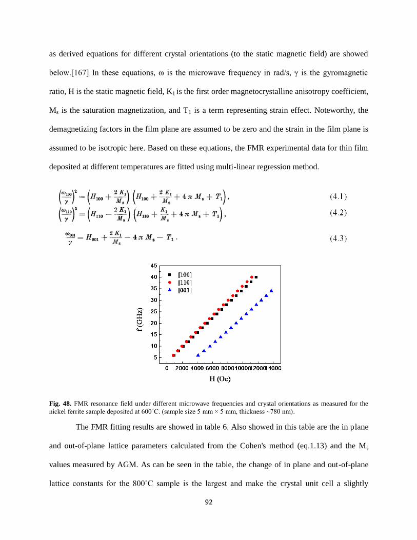
92
as derived equations for different crystal orientations (to the static magnetic field) are showed
below.[167] In these equations, ω is the microwave frequency in rad s, γ is the gyromagnetic
ratio, H is the static magnetic field, K1 is the first order magnetocrystalline anisotropy coefficient,
Ms is the saturation magnetization, and T1 is a term representing strain effect. Noteworthy, the
demagnetizing factors in the film plane are assumed to be zero and the strain in the film plane is
assumed to be isotropic here. Based on these equations, the FMR experimental data for thin film
deposited at different temperatures are fitted using multi-linear regression method.
Fig. 48. FMR resonance field under different microwave frequencies and crystal orientations as measured for the
nickel ferrite sample deposited at 600˚C. (sample size 5 mm × 5 mm, thickness ~780 nm).
The FMR fitting results are showed in table 6. Also showed in this table are the in plane
and out-of-plane lattice parameters calculated from the Cohen's method (eq.1.13) and the Ms
values measured by AGM. As can be seen in the table, the change of in plane and out-of-plane
lattice constants for the 800˚C sample is the largest and make the crystal unit cell a slightly

93
tetragonal shape, which indicates the existence of large tensile stress thin the film. This apparent
strain phenomenon will affect the internal magnetic field and thus change the resonance field.
The much smaller T1 term of 800 ˚C than those of other temperatures coincides with this strain
effect very well. Another behavior is the increasing magnetocrystalline anisotropy field (
)
with increasing deposition temperature, which might be attributed to the increased single crystal
quality of the as deposited thin films. The as listed spectroscopic splitting g factor (also known as
Landé g factor) has a relationship with the gyromagnetic ratio:
, in which and are
Bohr magneton and reduced Planck constant, respectively. The values of as calculated g factor
are slightly greater than 2, which has been also reported for experimental measurement of other
ferrite materials.[168]
Table 6. Structural and magnetic properties of nickel ferrite films deposited at different temperatures.
Structural and magnetic parameters Growth temperature (˚C)
500 600 700 800
In-plane lattice parameter a (Å) 8.354±0.002 8.346±0.002 8.348±0.003 8.366±0.001
Out-of-plane lattice parameter c (Å) 8.338±0.001 8.343±0.001 8.342±0.001 8.318±0.001
Saturation magnetization 4 MS (G) 3230 3280 3569 3757
g factor 2.24±0.003 2.27±0.01 2.28±0.009 2.28±0.03
2K1/MS (G) -75±15 -228±46 -272±38 -328±111
4 Meff (G) 2348±14 2560±46 2883±38 889±108
The line width of FMR resonance curve represents the degree of microwave loss which is
an important concern for practical microwave device application. Nickel ferrite films deposited
on MgAl2O4 at different temperatures were characterized by in plane FMR (static magnetic field
pointing at [100] direction) at microwave frequency of 9.5 GHz. The as measured thin film
thickness is in the range of (650~780 nm). As one can see in Fig.49, the FMR line width of film

94
deposited at 600˚C is the lowest. One important factor contributing to single crystal thin film
FMR line width is the surface roughness. This is probably the reason why films deposited at
higher temperatures show larger FMR linewidth. Another possible reason is interface diffusion
of Mg element from the substrate to the film at higher temperatures. Effect of chemical
impurities on FMR line width of ferrite materials has been widely investigated.[169,170] It's
noteworthy that the increased single crystal quality at higher temperatures is compromised by the
decreased FMR performance. Thin film deposited at 500˚C also shows larger FMR line width
than that of 600˚C. This might be attributed to the low single crystal quality and different ion
distribution in nickel ferrite lattice structure resulted from limited surface diffusion behavior at
low temperatures.
Fig. 49. Ferromagnetic resonance curve of nickel ferrite films deposited on MgAl2O4 substrate at different growth
temperatures. (Sample size 5 mm × 5 mm, thickness 650~780 nm) The inset shows the profile of FMR line width
with thin film growth temperature.
Due to the smallest FMR line width of films deposited at 600˚C, angle and frequency
dependence FMR behavior of film deposited at this temperature is characterized. The angle
dependence of in plane FMR line width measured at 9.5 GHz shows four-fold symmetry (Fig.50),
which coincides with the cubic structure of nickel ferrite as measured by XRD ϕ scan. In this

95
measurement, 0 degree represents the static magnetic field pointing at the [100] direction of the
single crystal. The in-plane cubic anisotropy can be clearly observed by the shift of the resonance
field at different orientations with the easier axis pointing at [110] direction. This is reasonable
considering that the easy axis is in the [111] direction in a bulk nickel ferrite single crystal.
Fig. 50. In plane FMR curves measured at different angles of the sample to the static magnetic field. The inset
shows the line width value vs. in plane angle.
The in plane and out-of-plane FMR curves are showed in Fig.51. As can be seen, both the
resonance field and the FMR line width have a big difference between the in plane and out-of-
plane measurement. The shift of the resonance field to a much higher position for the out-of-
plane measurement indicates the presence of a large magnetic anisotropy with easy axis parallel
to the thin film surface. The decreasing FMR line width from 752 to 160 Oe can be attributed to
the decreased two magnon scattering effect for the out-of-plane measurement.[171] It has been
proved that the coupling effect between the uniform FMR mode and degenerate spin waves is
angle dependent for thin film materials. More specifically, when the magnetic field is parallel to
the thin film surface, there are a large number of spin wave states which are degenerate with the
uniform mode and a significant contribution to the two magnon scattering line width is possible.
When the magnetic field is perpendicular to the thin film surface, there are essentially no spin
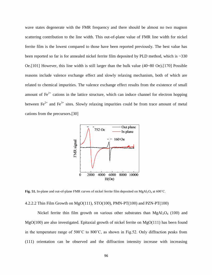
96
wave states degenerate with the FMR frequency and there should be almost no two magnon
scattering contribution to the line width. This out-of-plane value of FMR line width for nickel
ferrite film is the lowest compared to those have been reported previously. The best value has
been reported so far is for annealed nickel ferrite film deposited by PLD method, which is ~330
Oe.[101] However, this line width is still larger than the bulk value (40~80 Oe).[170] Possible
reasons include valence exchange effect and slowly relaxing mechanism, both of which are
related to chemical impurities. The valence exchange effect results from the existence of small
amount of Fe2+
cations in the lattice structure, which can induce channel for electron hopping
between Fe2+
and Fe3+
sites. Slowly relaxing impurities could be from trace amount of metal
cations from the precursors.[30]
Fig. 51. In-plane and out-of-plane FMR curves of nickel ferrite film deposited on MgAl2O4 at 600˚C.
4.2.2.2 Thin Film Growth on MgO(111), STO(100), PMN-PT(100) and PZN-PT(100)
Nickel ferrite thin film growth on various other substrates than MgAl2O4 (100) and
MgO(100) are also investigated. Epitaxial growth of nickel ferrite on MgO(111) has been found
in the temperature range of 500˚C to 800˚C, as shown in Fig.52. Only diffraction peaks from
(111) orientation can be observed and the diffraction intensity increase with increasing

97
deposition temperature. High resolution XRD measurement has showed that the as deposited thin
films have out-of-plane lattice parameters slightly smaller than the bulk value, which indicates
the existence of tensile stress in the thin films. This tensile stress is much smaller than those from
films grown on MgO (100) substrates and therefore no surface cracking has been observed for
films as thick as 1 micron. ω-scan and ϕ-scan have been carried out to characterize the out-of-
plane and in plane texture of the as deposited thin films. The FWHM values of the ω-scan of thin
films deposited at different temperatures are in the range of 0.6 to 0.7 and show decreasing trend
with increasing deposition temperature. Fig.53 shows the ϕ-scan result of nickel ferrite thin film
deposited on MgO(111) at 700˚C. The {400} and {200} planes of the nickel ferrite film and the
MgO substrate were scanned in plane. The three 120˚ separated peaks indicate the three-fold
symmetry of the (111) orientation and the match between those from film and substrate
represents the epitaxial growth.
Fig. 52. X-ray diffraction θ-2θ scan of nickel ferrite films grown on MgO(111) substrate at different temperatures.
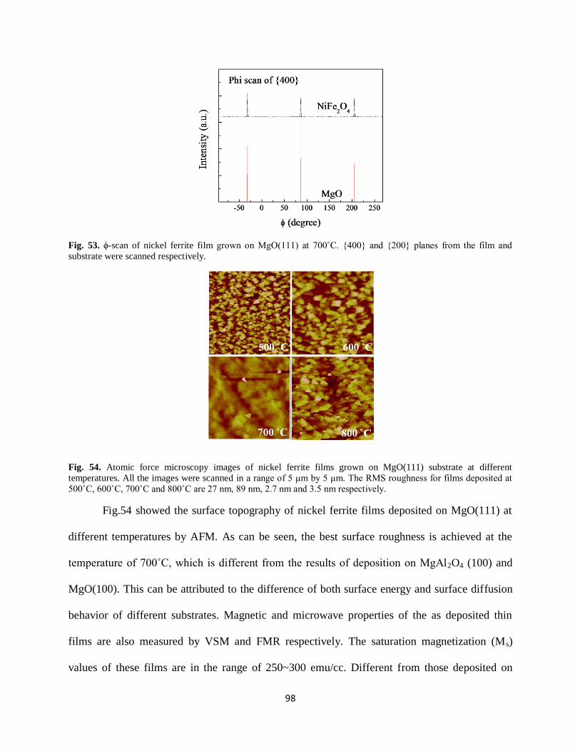
98
Fig. 53. ϕ-scan of nickel ferrite film grown on MgO(111) at 700˚C. {400} and {200} planes from the film and
substrate were scanned respectively.
Fig. 54. Atomic force microscopy images of nickel ferrite films grown on MgO(111) substrate at different
temperatures. All the images were scanned in a range of 5 μm by 5 μm. The RMS roughness for films deposited at
500˚C, 600˚C, 700˚C and 800˚C are 27 nm, 89 nm, 2.7 nm and 3.5 nm respectively.
Fig.54 showed the surface topography of nickel ferrite films deposited on MgO(111) at
different temperatures by AFM. As can be seen, the best surface roughness is achieved at the
temperature of 700˚C, which is different from the results of deposition on MgAl2O4 (100) and
MgO(100). This can be attributed to the difference of both surface energy and surface diffusion
behavior of different substrates. Magnetic and microwave properties of the as deposited thin
films are also measured by VSM and FMR respectively. The saturation magnetization (Ms)
values of these films are in the range of 250~300 emu/cc. Different from those deposited on

99
MgAl2O4, the Ms value decrease with increasing deposition temperature, which might result from
interface diffusion of Mg elements at high temperatures. The in plane FMR line width of these
films range from 900 to 1100 Oe showing decreasing trend with increasing temperature. The
improved surface roughness at high temperatures might contribute to the smaller FMR line width.
Annealing of these as deposited films at 1000˚C in air for certain time range (2 and 4 hrs) has
also been carried out to monitor the FMR line width change. All the films after annealing show
increased FMR line width, which is different from those reported results of PLD deposited nickel
ferrite films on MgO(111) substrate.[101]
Fig. 55. Epitaxial growth of nickel ferrite films on SrTiO3 (100), PMN-PT (100) and PZN-PT(100) substrates at
600˚C measured by XRD θ-2θ scan. Peaks with * are from (h00) reflections of the underlying substrates.
Nickel ferrite thin film growth on piezoelectric (ferroelectric) substrates SrTiO3 (100),
PMN-PT (100) and PZN-PT (100) are also investigated. All of these materials have a perovskite
structure with lattice constants of 3.905, 4.023, and 4.06 (for ideal cubic phase). The
corresponding lattice mismatch of nickel ferrite to these substrates are 6.4%, 3.5% and 2.5%,
respectively. DLICVD of nickel ferrite on these substrates have been carried out at 600˚C.
Epitaxial growth of nickel ferrite films has been observed, as shown in Fig.55. Film growth rate
around 700 nm/hr is achieved by using the same vaporizer conditions as deposition on MgAl2O4.

100
Surface roughness characterized by AFM showed much smoother growth on SrTiO3 (~1 nm)
than those on PMN-PT and PZNPT (~20 nm). Considering the similar atomic flat substrate
surface and film thickness, these difference of film surface roughness should be attributed to
different thin film growth mode due to different substrate surface energies. In-plane FMR
measurement (9.5 GHz) of nickel ferrite films deposited on these piezoelectric substrates show
FMR line width in the range of 800 to 1000 Oe. While the out-of-plane FMR curves are greatly
distorted, which indicates more defects/inhomogeneities in the as deposited thin films.
4.3 DLI-CVD Growth of LiFe5O8 Films
Lithium ferrite has the same inverse spinel structure as nickel ferrite, but it possesses a
much narrower FMR line width, which indicates very small microwave loss behavior. So far,
most of the reported lithium ferrite thin film deposition are based on physical vapor deposition
methods or liquid phase epitaxy.[89,93] No reports has been found by using metal organic
chemical vapor deposition technique. Our research on DLI-CVD of lithium ferrite films is novel
and can contribute to the understanding of thin film growth mechanism and proper processing
conditions.
In our research, Li(acac) and Fe(acac)3 are used as the metal organic precursors, both of
which are dissolved in DMF solvent in a molar ratio of 1:5. Typical vaporization and processing
conditions are listed in table 7. Most of the conditions are the same as those used for deposition
of nickel ferrite except for the concentration of the precursor solution. Thin film deposition on
MgAl2O4 (100) and MgO (100) are investigated in the temperature range of 500˚C to 800˚C. The
results of XRD characterization of as deposited films are showed in Fig.56. The results indicate
that epitaxial growth of lithium ferrite on MgO (100) can be obtained at all of the four
temperatures. Only (h00) reflections from lithium ferrite have been observed. As showed in

101
Fig.56(a), the (400) reflection peaks from lithium ferrite show doublet due to nonmonochromatic
X-ray (Cu Kα1 and Cu Kα2). With increasing deposition temperature, the peak shifts to lower 2θ
angles, which indicates an increasing out-of-plane lattice constant. The dashed line in the plot
marks where the bulk crystal value is. These results illustrate that with increasing deposition
temperature the stress in the as deposited films changes from tensile to compressive. This
phenomenon is resulted from both the effect of lattice mismatch and difference of thermal
expansion coefficient. Different from growth on MgO, films grown on MgAl2O4 do not show
any crystalline features at 500˚C and 600˚C as shown in Fig.56 (b). This is probably because of
the larger lattice mismatch between lithium ferrite and MgAl2O4. At higher temperatures, 700˚C
and 800˚C, weak diffraction peaks can be observed. However, peaks other than the epitaxial
orientation (h00) are also found in the deposition at 800˚C.
Table 7. Typical vaporization and processing conditions for DLI CVD of epitaxial LiFe5O8 films.
Substrate MgAl2O4 (100) / MgO (100)
Reaction pressure (Torr) 10
Growth temperature (˚C) 500-800
Concentration (Fe(acac)3, mol/L) 0.084
Concentration (Li(acac), mol/L) 0.0168
Solution flow rate (g/hr) 6
Ar carrier gas flow rate (sccm) 300
Vaporizer temperature (˚C) 175
Oxygen flow rate (sccm) 300

102
Fig. 56. X-ray diffraction θ-2θ characterization of lithium ferrite films deposited on (a) MgO (100) and (b) MgAl2O4
(100) substrate at different temperatures.
Surface morphology of the as deposited films on both substrates at different temperatures
are characterized by AFM. Films grown on MgO(100) show smooth surface with RMS values
around 1~2 nm. However, slight surface cracking is found for the films deposited at 500˚C,
which possess a relatively large tensile stress. It has been reported that CVD grown complex
oxide films likely exhibit surface cracking/crazing phenomenon when grown with a tensile
stress.[160] Films grown on MgAl2O4(100) show much larger surface roughness (~30 nm) and
there is no obvious temperature dependence. This result is quite different from the nickel ferrite
thin film growth, which is not so sensitive to the under lying substrate.
Due to the poor crystallinity and surface roughness, films grown on MgAl2O4 show
extremely low magnetic moment and wide and weak FMR curves. While films grown on
MgO(100) exhibit much better magnetic and microwave properties of lithium ferrite and are
introduced below. FMR measurement is sensitive to surface and bulk defects/inhomogeneities of
the thin film as introduced previously. In our work, only films deposited at 600˚C show
symmetric FMR curves and give the narrowest line width, as shown in Fig.57. As one can see in
this figure, the in plane FMR line width at 9.5 GHz is 368 Oe, which is much smaller than the

103
value of nickel ferrite films we have achieved. However, this value is still much larger than that
of the bulk crystal of lithium ferrite (< 10 Oe). Crystal defects and chemical inhomogeneities can
be the main reason for this large line width. Out-of-plane FMR measurement at the same
microwave frequency instead show very weak FMR signal and greatly distorted FMR curve,
which also indicates the presence of crystal defects or chemical inhomogeneities.
Fig. 57. In plane FMR measurement of lithium ferrite film grown on MgO(100) substrate at 600˚C. (The microwave
frequency is 9.5 GHz, the sample size is 5 mm by 5mm and film thickness is ~550 nm).
The saturation magnetization (Ms) of lithium ferrite films deposited on MgO(100) shows
increasing trend with increasing deposition temperature. This can be attributed to the increased
crystal quality of the films grown at higher temperatures. Similar to nickel ferrite films, FWHM
of the ω-scan decrease with increasing deposition temperature, which illustrates the increasing
single crystal quality. The Ms value for films deposited at 600˚C is around 200 emu cc, which is
much lower than the bulk value (350 emu/cc). The achievement of high Ms value has to be
compromised by a wider FMR line width.

104
4.4 Conclusion
In summary, we have used direct liquid injection-chemical vapor deposition (DLI-CVD)
for the growth of high quality epitaxial NiFe2O4 films on MgAl2O4 (100), MgO (100) and few
piezoelectric substrates. Anhydrous Ni(acac)2 and Fe(acac)3 precursor sources are dissolved in
DMF and vaporized under optimum conditions to generate stoichiometric concentration of the
cations in the gas phase for the CVD reaction. Appropriate oxygen flow with the precursors is
important both for improving the film morphology and also to obtain stoichiometric deposition.
Under our experimental conditions, film growth rate has been found in the range of 0.6-1.1
um/hr and can be further increased by increasing the solution concentration or liquid flow rate.
However, the vaporizer process condition and the oxygen flow rate also need to be adjusted to
maintain the desired film morphology and stoichiometry. Under optimized vaporization
conditions, the film morphology is dependent on the deposition temperature because of changes
in the surface diffusion behavior. In the temperature range of 600˚C to 700˚C, relatively thick
epitaxial NiFe2O4 films, which are extremely smooth and exhibit excellent magnetic properties,
have been deposited on both MgAl2O4 (100) and MgO (100) substrates. However, macroscopic
cracks develop on MgO after deposition and cool down, likely because of high residual tensile
stress. The increased saturation magnetization with increasing deposition temperature can be
attributed to improved crystalline quality, which is verified from X-ray diffraction and polarized
Raman measurements. The difference between in plane and out-of-plane FMR line width
measured at 9.5 GHz indicates the presence of two magnon scattering effect which is related to
crystal defects or chemical inhomogeneities in the films. FMR line width as low as ~160 Oe has
been achieved for out-of-plane measurement of nickel ferrite films deposited at 600˚C, which is
quite close to the value of bulk crystal.

105
DLI-CVD growth of lithium ferrite is investigated by using Li(acac) and Fe(acac)3 as the
metal organic precursors. Different from the deposition of nickel ferrite, lithium ferrite films
grown on MgAl2O4(100) are much rougher and do not show any crystalline features for
deposition at 500˚C and 600˚C. Spinel crystalline phases have been found for the deposition at
700˚C and 800˚C. However, more than one orientation are present for deposition at 800˚C.
Comparatively, lithium ferrite films deposited on MgO(100) exhibits single crystal quality and
much smoother surface for the deposition temperature range of 500˚C to 800˚C. The smaller
lattice mismatch between MgO and Nickel ferrite can be the principal reason. The narrowest in
plane FMR line width ~368 Oe has been found for the films deposited at 600˚C. With suitable
optimization of the vaporization and film deposition conditions, excellent quality ferrite films
can be grown at a relatively high rate using DLI-CVD.

106
CHAPTER 5. DIRECT LIQUID INJECTION CHEMICAL VAPOR DEPOSITION OF
FERROELECTRIC BARIUM TITANATE FILMS
5.1 Introduction
As previously introduced, barium titanate (BaTiO3) possesses excellent properties (high
dielectric constants, ferroelectric, optoelectronic, etc.,) for application in certain advanced
electronic devices, and great efforts have been dedicated to the deposition of high quality single
crystal barium titanate thin films in the past decades.[113-115] Among these studies, chemical
vapor deposition is uniquely preferred due to its capability of large area and conformal
deposition. One challenge for CVD growth of barium titanate thin film is the availability of
volatile and thermally stable barium precursor. The use of metal organic β-diketonate barium
precursor Ba(thd)2 {bis(2,2,6,6-tetramethyl-3,5-heptanedionato) barium (II)} has been widely
studied in CVD method, but the high temperature (~250˚C) needed to vaporize the solid
precursor would result in precursor degradation (sintering effect) and thus affect run to run
repeatability.[135,138,139] Besides, the precise control of rate of introduction of barium
precursor into the reaction chamber is almost impossible. In this chapter, DLICVD technique as
used in the deposition of nickel ferrite is used for deposition of barium titanate films. For this
technique, by dissolving metal organic precursors into an appropriate solvent, few advantages
can be achieved over direct vaporization of the solid phase precursors. For example, low
vaporization temperature, accurate control of liquid flow rate, and minimization of precursor
oligomerization effect, etc.. In our work, Ba(hfa)2•tetraglyme {Ba(C5HF6O2)•(C10H22O5)} and
Ti(thd)2(OPri)2 {Ti(C11H19O2)2(C3H7O)2} are dissolved in toluene as the precursor source. The
107
vaporization and CVD processing conditions are both studied to examine their effects on the as
grown thin film quality. Chemical composition, surface and bulk morphology and
crystallographic information of the as grown thin films are characterized to monitor the thin film
quality. Preliminary results of epitaxial growth of barium titanate thin film on MgO (100)
substrate have been achieved and are reported in this chapter.
5.2 Experimental Details
In this work, the same DLI-CVD system as used for the deposition of nickel ferrite is
used for the deposition of barium titanate, as shown in Fig.38. Ba(hfa)2•tetraglyme (m.p. 153˚C)
and Ti(thd)2(OPri)2 (m.p. ~180˚C) are used as metal organic precursors. The Ba precursor is
synthesized from Ba(OH)2•8H2O following the method reported by Malandrino, et. al., [172] and
the Ti precursor is bought from Sigma-Aldrich and used without any further purification. Both
precursors are dissolved in Toluene (C6H5CH3, b.p. 110.6˚C) in a molar ratio of 1:1. Atomically
polished MgO (100) single crystal (a=4.21Å, 5mm×5mm×0.5mm) from CrysTec Gmbh is used
as the substrate and ultrasonically cleaned sequentially by acetone and isopropanol before loaded
into the CVD reactor. Processing conditions for a typical reaction are substrate temperature 750
˚C, precursor concentration 0.1 M, precursor flow rate 6 g/hr, vaporizer temperature 150 ˚C,
reaction pressure 10 torr, carrier gas (Ar) flow rate 250 sccm and oxygen flow rate 300 sccm. It
is important that the oxygen flow is bubbled through water in this case to eliminate formation of
a BaF2 phase (F eliminated by forming HF). The connection tubing from the vaporizer to the
CVD reaction chamber is wrapped by heating tapes and heated to ~10 ˚C above the vaporizer
temperature to avoid vapor condensation on the tubing walls. The oxygen (research grade) gas is
preheated to a temperature close to the vaporizer temperature before it's delivered into the
reaction chamber to minimize its effect on the vapor quality (gas phase condensation). The
108
reaction zone of the tube furnace is heated to the reaction temperature in a heating rate of ~15
˚C/min and stabilized at the deposition temperature for ~30 min before CVD reaction. The
vaporize is preheated to the designated temperature with carrier gas flow and stabilize for ~30
min. When the liquid precursor source is introduced into the vaporizer, its first directed into the
exhaust by passing through the by-pass line, as shown in Fig.38. The vaporization process is
stabilized for ~15 min before the valve to the reaction chamber is opened, from when the CVD
reaction is started. A cooling trap with liquid nitrogen is used to trap the organic solvent or
reaction by products to minimize contamination of pump oil (rotary vane vacuum pump). The as
deposited thin film characterization by various techniques are introduced below.
Chemical composition of the as deposited films are characterized by both XPS and EDX.
For the XPS (PHI/APEX) measurement, non-monochromatic Al Kα (1486.6 eV) X-ray is used to
irradiate the sample surface. Analysis area around 2 mm by 2 mm is selected by setting the
appropriate electron entrance and exit slit size of the hemispherical electron spectrometer. For a
typical XPS measurement, the X-ray beam power is set to 100W, the electron pass energy is set
to 100 eV for a survey measurement and 25 eV for a high resolution measurement, and the
electron take off angle is set to 45˚. The EDX detector is installed in a SEM system (JEOL/7000).
A typical EDX measurement has electron beam energy of 20 KV, spot size of 8 and working
distance of 10 mm. Measurements from few areas are averaged to get the final composition
results. XRD (Philips X’pert Pro) is used to investigate crystallographic properties of the as-
deposited films. Cu Kα (1.5418 Å) radiation is used as the X-ray source. All the samples are
characterized under similar experimental conditions (with a nickel filter and 0.5˚ divergence slit
size). For the rocking curve analysis, 2θ was fixed at the NiFe2O4 (200) diffraction angle of
barium titanate while scanning ω. For the SEM characterization, electron beam conditions are
109
the same as those mentioned for EDX measurement. All the samples are attached to the sample
holder by carbon tape and no metallic coatings on the sample surfaces are deposited. For the
AFM (Digital instruments/ Nanoscope IV) characterization, ultra sharp non-contact silicon
cantilevers (MikroMasch, NSC15/AIBS) with a typical probe tip radius of ~10nm and resonant
frequency of ~325 kHz are used in tapping mode.
5.3 Results and Discussion
The vaporization conditions of our DLI vaporizer for the specific precursor solution,
Ba(hfa)2•tetraglyme and Ti(thd)2(OPri)2 in toluene, are optimized by checking the as deposited
thin film quality. It has been found that the liquid flow rate, carrier gas flow rate, and vaporizer
pressure and temperature work together to give high quality vapor phase. When the precursor
source solution is not properly vaporized, large deviation of thin film stoichiometry or surface
morphology could be observed. An optimized combination of vaporization conditions has been
listed in the experimental details (5.2) and preliminary results of epitaxial barium titanate thin
film growth under these vaporization conditions are showed below.
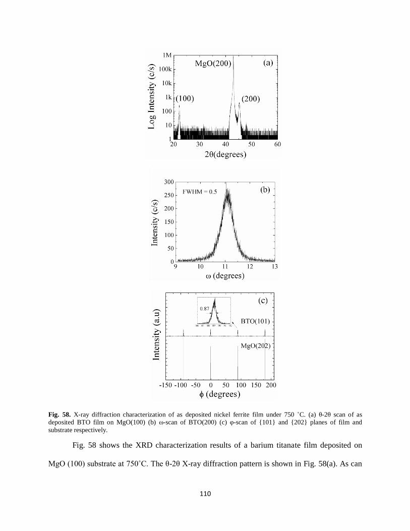
110
Fig. 58. X-ray diffraction characterization of as deposited nickel ferrite film under 750 ˚C. (a) θ-2θ scan of as
deposited BTO film on MgO(100) (b) ω-scan of BTO(200) (c) φ-scan of {101} and {202} planes of film and
substrate respectively.
Fig. 58 shows the XRD characterization results of a barium titanate film deposited on
MgO (100) substrate at 750˚C. The θ-2θ X-ray diffraction pattern is shown in Fig. 58(a). As can

111
be seen, the film grows with single orientation in the normal direction, since X-ray spectrum of
BTO film shows only reflections from (h00) crystallographic planes the same as those of MgO
substrate. According to this X-ray data, the out-of-plane lattice constant of BTO film is found to
be 4.007Å, which is a value between a and c lattice constants (a =3.992Å, c =4.032Å) of BTO
crystal at room temperature.[111] It’s impossible to identify the thin film growth in a or c
orientation based on this result. Moreover, the peak shift can be also attributed to the interfacial
stress. Out-of-plane and in plane texture of this sample are examined by ω and φ scan as shown
in Fig.58 (b) and (c). The measured FWHM (full-width-at-half-maximum) value of ω-scan of
BTO(200) is 0.5˚, which is about in the middle of those have been reported (0.23~0.9).
[117,130,138,139] The φ-scan of {101} planes of both BTO film and MgO substrate shows the
four coincidently 90˚ separated peaks. This result illustrated the four fold symmetry of both the
BTO and MgO lattice. Meanwhile, the coincidence of peaks positions indicate a cube on cube
epitaxial relationship.
Fig. 59. (a) Cross sectional view of BaTiO3 on MgO by SEM (b) Surface view of BaTiO3 film on MgO; inlet shows
a 10 μm by 10 μm AFM image of the same surface with RMS roughness around 20 nm.
Cross sectional and surface morphology of the as deposited BaTiO3 film on MgO has
been characterized by SEM and AFM. As seen in Fig. 59(a), the cross section of a ~0.5 μm thick
(1 hour deposition) BaTiO3 film on MgO substrate presents certain defects, especially at the

112
interface. This phenomenon probably results from island mode film growth at a high deposition
temperature. Chemical composition of this film is characterized by the Energy Dispersive X-ray
spectroscopy (EDX) equipped in the SEM system. The ratio of Ba to Ti is quite close to 1:1 as
expected. No F or C element has been detected by this technique. The oxygen concentration is
not considered due to external signals from the MgO substrate. The surface morphology of
BaTiO3 films are both studied by SEM and AFM, as shown in Fig. 59(b). The AFM measured
grain size is around ~1 μm and RMS roughness is ~20nm.
Fig. 60. Fluorine peak is present in the XPS spectrum of as deposited barium titanate thin film surface.
The thin film surface is also characterized by XPS, as shown in Fig.60. Except for the Ba,
Ti, and O elements, F (~4 at%) is also detected. The C peak is from adventitious carbon of air
contamination (284.8 eV). Different from EDX, which has a detection thickness around 1~2 μm,
XPS is a surface sensitive technique (few nm detection thickness) and much more sensitive to
small elements like F. High resolution scan of the F peak has showed the peak position is at
~684.7 eV, which indicates the existence of metal fluoride bond. In this case, it's probably Ba-F
bond.[129] Besides, this value is a little higher than the reported value of 684.3 eV for F 1s in
pure BaF2, which can be attributed to the different chemical environment.[173] Although the

113
XRD characterization has showed pure BaTiO3 phase, F elements can still exist in the film in
amorphous phase and affect thin film physical property.
5.4 Conclusion
Epitaxial growth of BaTiO3 films on MgO (100) substrate has been obtained by DLI-
CVD technique. Good single crystal quality has been illustrated by the results of ω and ϕ-scan.
Thin film growth rate of ~0.5 μm hr is achieved under our experimental conditions. Surface and
cross sectional morphology characterization shows large surface roughness and interface voids,
which can be contributed to the island mode thin film growth. Incorporation of small amount of
F elements in the thin film has been verified by XPS analysis. Instead of forming crystalline
BaF2 phase, the F elements bonds to the Ba ions in amorphous state.
Although we have obtained epitaxial growth of BTO films, few issues related to thin film
quality still need to be improved, such as the film morphology, growth rate, and chemical
contamination. Either optimizing CVD processing conditions or selecting more appropriate Ba
precursor is believed to be capable of improving these issues in certain degree.

114
CHAPTER 6. CONCLUSION AND FUTURE WORK
6.1 Conclusion
Chemical vapor deposition (CVD) of thin film materials with excellent electronic or
magnetic properties has been investigated in this dissertation. Specific CVD techniques including
plasma enhanced atomic layer deposition (PEALD) and direct liquid injection CVD (DLI-CVD)
have been employed based on the requirements of practical thin film application. The essential
work consists of chemical precursor selection and characterization, CVD processing, and thin
film characterization. The results of thin film characterization could provide important
information for the optimization of CVD processing conditions and thus in turn to improve the
thin film quality. The results of PEALD of hafnium nitride (HfN), DLI-CVD of nickel ferrite
(NiFe2O4), lithium ferrite (LiFe5O8), and barium titanate (BaTiO3) are summarized below.
6.1.1 PEALD of HfN thin films
Tetrakis (dimethylamido) hafnium (IV) (TDMAH) is used as the metal organic precursor
for PEALD of HfN thin film. Its adsorption and reaction on hydrogenated Si(100) surface has
been investigated by in-situ ATR-FTIR. It has been found that for temperatures below 100˚C,
physisorption is the main mode of TDMAH adsorbing onto the crystal surface and no obvious
surface Si-H bonds breaking. These physisorbed TDMAH molecules have weak bonding energy
to the surface and easy to desorb. At temperatures between 100˚C and 150˚C, surface adsorbed
TDMAH molecules start to decompose and newly emerging IR peaks at 1591 cm-1
and 1639 cm-
1 are assigned to N=C and Hf-H vibrational mode respectively based on a β-hydride elimination
mechanism. The decomposition species on the surface has been found hard to desorb at 150˚C,
115
which can contaminate the thin film growth if the purging/pumping time is not long enough. The
surface Si-H bonds subtraction has been found for adsorption above 150˚C and it is closely
related to the TDMAH decomposition behavior.
Hafnium nitride thin film deposition by PEALD using TDMAH and hydrogen plasma has
been investigated. Uniform and moderately conductive HfNxCy thin films were deposited on
Si(100) and SiO2 substrates. A thin surface layer (2~3 nm) containing both hafnium nitride and
organic complexes of TDMAH decomposition has been found by in vacuo XPS analysis. Depth
profile analysis by XPS indicated the existence of hafnium carbide phase in the bulk. Thin film
resistivity is greatly affected by the level of hydrogen plasma power, in which higher plasma
power results in lower thin film resistivity. In spite of this tunability of resistivity by plasma
power, carbon incorporation is still an issue for this PEALD method.
6.1.2 DLI-CVD of nickel ferrite and lithium ferrite films
We have used DLI-CVD technique for the growth of high quality epitaxial NiFe2O4 films
on MgAl2O4 (100), MgO (100), MgO (111) and few piezoelectric substrates. Anhydrous
Ni(acac)2 and Fe(acac)3 precursor sources are dissolved in DMF and vaporized under optimum
conditions to generate stoichiometric concentration of the cations in the gas phase for the CVD
reaction. Appropriate oxygen flow with the precursors is important both for improving the film
morphology and also to obtain stoichiometric deposition. Under our experimental conditions,
film growth rate has been found in the range of 0.6-1.1 um/hr and can be further increased by
increasing the solution concentration or liquid flow rate. However, the vaporizer process
condition and the oxygen flow rate also need to be adjusted to maintain the desired film
morphology and stoichiometry. Under optimized vaporization conditions, the film morphology is
dependent on the deposition temperature because of changes in the surface diffusion behavior. In

116
the temperature range of 600˚C to 700˚C, relatively thick epitaxial NiFe2O4 films, which are
extremely smooth and exhibit excellent magnetic properties, have been deposited on both
MgAl2O4 (100) and MgO (100) substrates. However, macroscopic cracks develop on MgO after
deposition and cool down, likely because of high residual tensile stress. The increased saturation
magnetization with increasing deposition temperature can be attributed to improved crystalline
quality, which is verified from X-ray diffraction and polarized Raman measurements. The
difference between in plane and out-of-plane FMR line width measured at 9.5 GHz indicates the
presence of two magnon scattering effect which is related to crystal defects or chemical
inhomogeneities in the films. FMR line width as low as ~160 Oe has been achieved for out-of-
plane measurement of nickel ferrite films deposited at 600˚C, which is quite close to the value of
bulk crystal.
DLI-CVD growth of lithium ferrite is investigated by using Li(acac) and Fe(acac)3 as the
metal organic precursors. Different from the deposition of nickel ferrite, lithium ferrite films
grown on MgAl2O4(100) are much rougher and do not show any crystalline features for
deposition at 500˚C and 600˚C. Spinel crystalline phases have been found for the deposition at
700˚C and 800˚C. However, more than one orientation are present for deposition at 800˚C.
Comparatively, lithium ferrite films deposited on MgO(100) exhibits single crystal quality and
much smoother surface for the deposition temperature range of 500˚C to 800˚C. The smaller
lattice mismatch between MgO and Nickel ferrite can be the principal reason. The narrowest in
plane FMR line width ~368 Oe has been found for the films deposited at 600˚C. With suitable
optimization of the vaporization and film deposition conditions, excellent quality ferrite films
can be grown at a relatively high rate using DLI-CVD.

117
6.1.3 DLI-CVD of barium titanate films
Epitaxial growth of BaTiO3 films on MgO (100) substrate has been obtained by DLI-
CVD technique. Good single crystal quality has been illustrated by the results of ω and ϕ-scan.
Thin film growth rate of ~0.5 μm hr is achieved under our experimental conditions. Surface and
cross sectional morphology characterization shows large surface roughness and interface voids,
which can be contributed to the island mode thin film growth. Incorporation of small amount of
F elements in the thin film has been verified by XPS analysis. Instead of forming crystalline
BaF2 phase, the F elements bonds to the Ba ions in amorphous state.
6.2 Future work
PEALD of HfN by using TDMAH and hydrogen plasma has been limited by thin film
contamination from incorporation of C. In spite of the increased conductivity of thin films
deposited at high plasma powers, the C concentration is not affected much by the plasma power.
This is directly related to the chemical reaction mechanisms between TDMAH and hydrogen
plasma. To improve the as deposited thin film quality, substrates with smaller lattice mismatch
can be selected, such as MgO(100) (7%). To improve the thin film purity, more appropriate
reducing agent than hydrogen plasma should be selected. Dimethyl hydrazine (H2NN(CH3)2),
which has been successfully used in thermal CVD of HfN thin films, might be a good candidate
for this PEALD experiment to replace hydrogen.[70] Potential advantages include: low plasma
power is needed to break the weak N=N bond and the -NH2 group is more readily to react with
the central Hf atom and work as an external N source.[174]
Single crystalline spinel ferrite films, including nickel ferrite and lithium ferrite, have
been successfully deposited on certain small lattice match substrates by DLI-CVD method. For
nickel ferrite deposition, more work can be focused on the deposition on piezoelectric substrates,

118
such as PMN-PT and PZN-PT. CVD processing conditions can be tuned to optimize the physical
properties of as deposited films and thus provide high quality films for the fundamental research
in ferrite-ferroelectric layered heterostructures. A MgO buffer layer can be grown on these
piezoelectric substrates to minimize the lattice mismatch and improve thin film morphology. For
lithium ferrite thin film growth, substrate with spinel structure and smaller lattice mismatch, such
as MgGa2O4 (a=8.28 Å, 0.6%)[175] and CoGa2O4 (a=8.32 Å, 0.1%)[176] can be tried for thin
film growth. The goal is to achieve both high saturation magnetization and narrow FMR line
width.
For the deposition of barium titanate by DLI-CVD technique, incorporation of F in the
thin film from the fluorinated Ba precursor has been found. One way to improve is to use
stronger oxidizing agent such as ozone (O3) or hydrogen peroxide (H2O2). The other way is to
employ new Ba precursors without F elements in the molecule. For example, Ba(thd)2
{bis(2,2,6,6-tetramethyl-3,5-heptanedionato) barium (II)} or its polyether adduct can be tried.
However, due to its low volatility, the vaporizer conditions have to be tuned accordingly.

119
REFERENCES
[1]. M. Leong, B. Doris, J. Kedzierski, K. Rim, M. Yang, Science 2004, 306, 2057.
[2]. M. N. Baibich, J. M. Broto, A. Fert, F. Nguyen Van Dau, F. Petroff, P. Eitenne, G. Creuzet,
A. Friederich, J. Chazelas, Phys. Rev. Lett. 1988, 61, 2472.
[3]. J. S. Moodera, G. X. Miao, T. S. Santos, Physics Today 2010, 63, 46.
[4]. W. Eerenstein, N. D. Mathur, J. F. Scott, Nature 2006, 442, 759.
[5]. F. Zaera, J. Mater. Chem. 2008, 18, 3521.
[6]. D. Beaulieu, Y. Ding, Z. L. Wang, W. J. Lackey, J. Vac. Sci. Technol. B 2005, 23, 2151.
[7]. K. F. Jensen, Annu. Rev. Fluid Mech. 1991, 23, 197.
[8]. S. M. George, Chem. Rev. 2010, 110, 111.
[9]. Z. Li, R. G. Gordon, V. Pallem, H. Li, D. V. Shenai, Chem. Mater. 2010, 22, 3060.
[10]. M.-K. Song, S.-W. Kang, S.-W. Rhee, Thin Solid Films 2004, 450, 272.
[11]. Thin Film Deposition: Principles and Practice (D. L. Smith), McGraw-Hill, Inc., New York
1995.
[12]. Chemical Vapor Deposition: Principles and Applications (M.-L. Hitchman, K.-F. Jensen),
Academic Press, London 1993.
[13]. M. Leskelä, M. Ritala, Thin Solid Films 2002, 409, 138.
[14]. K. R. Bray, G. N. Parsons, Phys. Rev. B 2001, 65, 035311.
[15]. B. Daudin, F. Widmann, G. Feuillet, Y. Samson, M. Arlery, J. L. Rouvière, Phys. Rev. B
1997, 56, R7069.
[16]. M. T. Currie, S. B. Samavedam, T. A. Langdo, C. W. Leitz, E. A. Fitzgerald, Appl. Phys. Lett.
1998, 72, 1718.
[17]. R. N. Jacobs, J. Markunas, J. Pellegrino, L. A. Almeida, M. Groenert, M. Jaime-Vasquez, N.
Mahadik, C. Andrews, S. B. Qadri, J. Cryst. Growth 2008, 310, 2960.

120
[18]. L. S.-J. Peng, X. X. Xi, B. H. Moeckly, S. P. Alpay, Appl. Phys. Lett. 2003, 83, 4592.
[19]. Introduction to Infrared and Raman Spectroscopy (N. B. Colthup, L. H. Daly, S. E.
Wiberley), Academic Press, New York 1990.
[20]. Infrared Characterization for Microelectronics (W. S. Lau), World Scientific, New Jersey
1999.
[21]. Internal Reflection Spectroscopy (N. J. Harrick), John Wiley & Sons, New York 1967.
[22]. P. J. Cumpson, J. Electron Spectrosc. Relat. Phenom. 1995, 73, 25.
[23]. Handbook of X-ray Photoelectron Spectroscopy (J. F. Moulder, W. F. Stickle, P. E. Sobol, K.
D. Bomben), Physical Electronics 1995.
[24]. Thin Film Analysis by X-ray Scattering (Mario Berkholz), WILEY-VCH Verlag GmbH& Co.
KGaA, WeinHeim 2006.
[25]. M. U. Cohen, Rev. Sci. Instrum. 1935, 6, 68.
[26]. S. Okamoto, O. Kitakami, Y. Shimada, J. Magn. Magn. Mater. 2000, 208, 102.
[27]. G. Binnig, C. F. Quate, C. Gerber, Phys. Rev. Lett. 1986, 56, 930.
[28]. Spin Waves: Theory and Applications (D. D. Stancil, A. Prabhakar), Springer, New York
2009.
[29]. M. P.-Horvath, J. Magn. Magn. Mater. 2000, 215-216, 171.
[30]. Ferromagnetic-Relaxation Theory (Marshall Sparks), McGraw-Hill, New York 1964.
[31]. B. K. Kuanr, R. E. Camley, Z. Celinski, J. Appl. Phys. 2004, 95, 6610.
[32]. S. J. Yuan, L. Wang, R. Shan, S. M. Zhou, Appl. Phys. A 2004, 79, 701.
[33]. CMOS: Circuit Design, Layout, and Simulation (R. J. Baker), Wiley& Sons Inc., Hoboken,
New Jersey 2010.
[34]. J. Aarik, A. Aidla, H. Mändar, T. Uustare, K. Kukli, M. Schuisky, Appl. Surf. Sci. 2001, 173,
15.
[35]. H. Kato, T. Nango, T. Miyagawa, T. Katagiri, K. S. Seol, Y. Ohki, J. Appl. Phys. 2002, 92,
1106.
[36]. M.-H. Cho, Y. S. Roh, C. N. Whang, K. Jeong, S. W. Nahm, D. -H. Ko, J. H. Lee, N. I. Lee,
K. Fujihara, Appl. Phys. Lett. 2002, 81, 472.
121
[37]. F. Fillot, T. Morel, S. Minoret, I. Matko, S. Maîtrejean, B. Guillaumot, B. Chenevier, T.
Billon, Microelectron. Eng. 2005, 82, 248.
[38]. J. K. Schaeffer, S. B. Samavedam, D. C. Gilmer, V. Dhandapani, P. J. Tobin, J. Mogab, B. -
Y. Nguyen, B. E. White, Jr., S. Dakshina-Murthy, R. S. Rai, Z. -X. Jiang, R. Martin, M. V.
Raymond, M. Zavala, L. B. La, J. A. Smith, R. Garcia, D. Roan, M. Kottke, R. B. Gregory, J.
Vac. Sci. Technol. B 2003, 21, 11.
[39]. Y. T. Hou, F. Y. Yen, P. F. Hsu, V. S. Chang, P. S. Lim, C. L. Hung, L. G. Yao, J. C. Jiang,
H. J. Lin, Y. Jin, S. M. Jang, H. J. Tao, S. C. Chen, M. S. Liang, Electron Device Meeting,
IEDM Technical Digest. IEEE international 2005, 5-5, 31.
[40]. Q. X. Jia, J. R. Groves, P. Arendt, Y. Fan, A. T. Findikoglu, S. R. Foltyn, H. Jiang, F. A.
Miranda, Appl. Phys. Lett. 1999, 74, 1564.
[41]. W. J. Kim, W. Chang, S. B. Qadri, H. D. Wu, J. M. Pond, S. W. Kirchoefer, H. S. Newman,
D. B. Chrisey, J. S. Horwitz, Appl. Phys. A 2000, 71, 7.
[42]. V. E. Demidov, B. A. Kalinikos, P. Edenhofer, J. Appl. Phys. 2002, 91, 10007.
[43]. A. A. Semenov, S. F. Karmanenko, V. E. Demidov, B. A. Kalinikos, Appl. Phys. Lett. 2006,
88, 033503.
[44]. A. A. Semenov, S. F. Karmanenko, B. A. Kalinikos, A. N. Slavin, G. Srinivasan, J. V.
Mantese, Integr. Ferroelectr. 2005, 75, 199.
[45]. A. S. Tatarenko, A. B. Ustinov, G. Srinivasan, V. M. Petrov, M. I. Bichurin, J. Appl. Phys.
2010, 108, 063923.
[46]. Y. -Y. Song, J. Das, P. Krivosik, N. Mo, C. E. Patton, Appl. Phys. Lett. 2009, 94, 182505.
[47]. S. Shinkai, K. Sasaki, Jpn. J. Appl. Phys. 1999, 38, 2097.
[48]. Y. Gotoh, M. Liao, H. Tsuji, J. Ishikawa, Jpn. J. Appl. Phys. 2003, 42, L778.
[49]. R. Fujii, Y. Gotoh, M. Y. Liao, H. Tsuji, J. Ishikawa, Vacuum 2006, 80, 832.
[50]. M. H. Staia, D. G. Bhat, E. S. Puchi-Cabrera, J. Bost, Wear 2006 261, 540.
[51]. J. J. Oakes, Thin Solid Films 107 (1983) 159.
[52]. H. Y. Yu, J. F. Kang, C. Ren, J. D. Chen, Y. T. Hou, C. Shen, M. F. Li, D. S. H. Chan, K. L.
Bera, C. H. Tung, D.-L. Kwong, IEEE Elec. Dev. Lett. 2004, 25, 70.
[53]. R. Nowak, C.L. Li, Thin Solid Films 1997, 305, 297.

122
[54]. B. O. Johansson, J. –E. Sundgren, U. Helmersson, M.K. Hibbs, Appl. Phys. Lett. 1984, 44,
670.
[55]. P. R. Aron, A. Grill, Thin Solid Films 1982, 96, 87.
[56]. M. Y. Liao, Y. Gotoh, H. Tsuji, J. Ishikawa, J. Vac. Sci. Technol. A 2004, 22, 214.
[57]. L. Yuan, G. Fang, C. Li, M. Wang, N. Liu, L. Ai, Y. Cheng, H. Gao, X. Zhao, Appl. Surf. Sci.
2007, 253, 8538.
[58]. Y. Gotoh, M.Y. Liao, H. Tsuji, J. Ishikawa, Jpn. J. Appl. Phys. 2003, 42, L778.
[59]. R. A. Araujo, X. Zhang, H. Wang, J. Electron. Mater. 2008, 37, 1828.
[60]. A. Arranz, Surf. Sci. 2004, 563, 1.
[61]. K. Volz, M. Kiuchi, W. Ensinger, Surf. Coat. Technol. 1999, 120-121, 353.
[62]. R. Fix, R.G. Gordon, D.M. Hoffman, Chem. Mater. 1991, 3, 1138.
[63]. D. M. Hausmann, E. Kim, J. Becker, R. G. Gordon, Chem. Mater. 2002, 14, 4350.
[64]. H. Itoh, K. Kato, K. Sugiyama, J. Mater. Sci. 1986, 21, 751.
[65]. D. M. Hoffman, Polyhedron 1994, 13, 1169.
[66]. J. H. Jang, T. J. Park, J. H. Kim, K. D. Na, W. Y. Park, M. Kim, C. S. Hwang, J.
Electrochem. Soc. 2009, 156, H76.
[67]. J. S. Becker, E. Kim, R. G. Gordon, Chem. Mater. 2004, 16, 3497.
[68]. W. Wang, T. Nabatame, Y. Shimogaki, Microelectron. Eng. 2008, 85, 320.
[69]. W. Wang, T. Nabatame, Y. Shimogaki, Jpn, J. Appl. Phys. 2004, 43, L1445.
[70]. Y. Kim, A. Baunemann, H. Parala, A. Devi, R.A. Fischer, Chem. Vap. Deposition 2005,
11, 294.
[71]. E. J. Kim, D. H. Kim, Electrochem. Solid State Lett. 2006, 9, C123.
[72]. S. Consiglio, W. Zeng, N. Berliner, E.T. Eisenbraun, J. Electrochem. Soc. 2008, 155, H196.
[73]. V. G. Harris, A. Geiler, Y. Chen, S. D. Yoon, M. Wu, A. Yang, Z. Chen, P. He, P. V. Parimi,
X. Zuo, C. E. Patton, M. Abe, O. Acher, C. Vittoria, J. Magn. Magn. Mater. 2009, 321, 2035.
[74]. C. N. Chinnasamy, A. Narayanasamy, N. Ponpandian, K. Chattopadhyay, K. Shinoda, B.
123
Jeyadevan, K. Tohji, K. Nakatsuka, I. Nakatani, Phys. Rev. B 2001, 63, 184108.
[75]. E. Rezlesku, L. Sachelarie, P. D. Popa, N. Rezlesku, IEEE Trans. Magn. 2000, 36, 3962.
[76]. W. G. Nilsen, R. L. Comstock, J. P. Remeika, J. Appl. Phys. 1966, 37, 1224.
[77]. M. I. Bichurin, V. M. Petrov, G. Srinivasan, Phys. Rev. B. 2003, 68, 054402.
[78]. M. Pardavi-Horvath, J. Magn. Magn. Mater. 2000, 215-216, 171.
[79]. P. Gibart, M. Robbins, A. B. Kane, J. Cryst. Growth 1974, 24, 166.
[80]. J. ŠıмšоѵÁ, Czech. J. Phys. B. 1970, 20, 727.
[81]. J. E. Mee, G. R. Pulliam, J. L. Archer, P. J. Besser, IEEE Trans. Magn. 1969, 5, 717.
[82]. A. G. Fitzgerald, R. Engin, Thin Solid Films 1974, 20, 317.
[83]. P. A. Lane, P. J. Wright, M. J. Crosbie, A. D. Pitt, C. L. Reeves, B. Cockayne, A. C. Jones, T.
J. Leedham, J. Cryst. Growth 1998, 192, 423.
[84]. A. G. Fitzgerald, J. Mat. Sci. 1987, 22, 1887.
[85]. J. F. Roeder, S. M. Bilodeau, R. J. Carl, T. H. Baum, P. C. Vanbuskirk, R. R. Woolcott, A. I.
Kingon, Mat. Res. Soc. Symp. Proc. 1997, 474, 21.
[86]. E. J. Donahue, D. M. Schleich, J. Appl. Phys. 1992, 71, 6013.
[87]. S. Pignard, H. Vincent, J. P. Sénateur, Thin Solid Films 1999, 350, 119.
[88]. J. Lee, B. Lee, S. Joo, IEEE Trans. Magn. 1999, 35, 3415.
[89]. P. Samarasekara, F. J. Cadieu, Chin. J. Phys. 2001, 39, 635.
[90]. E. Suzuki, Y. Hoshi, M. Naoe, J. Appl. Phys. 1998, 83, 6250.
[91]. S. Capraro, J. P. Chatelon, H. Joisten, M. Le Berre, B. Bayard, D. Barbier, J. J. Rousseau, J.
Appl. Phys. 2003, 93, 9898.
[92]. J. M. Robertson, M. Jansen, B. Hoekstra, P. F. Bongers, J. Cryst. Growth 1977, 41, 29.
[93]. H. L. Glass, J. H. W. Liaw, Mat. Res. Bul. 1978, 13, 353.
[94]. S. D. Yoon, C. Vittoria, J. Appl. Phys. 2003, 93, 8597.
[95]. S. D. Yoon, C. Vittoria, J. Magn. Magn. Mater. 2004, 272-276, e1833.

124
[96]. J. D. Adam, S. V. Krishnaswamy, S. H. Talisa, K. C. Yoo, J. Magn. Magn. Mater. 1990, 83,
419.
[97]. J. L. Deschanvres, M. Langlet, J. C. Joubert, J. Magn. Magn. Mater. 1990, 83, 437.
[98]. J. M. Phillips, R. B. Vandover, E. M. Gyorgy, J. H. Marshall, Mat. Res. Soc. Symp. Proc.
1994, 317, 589.
[99]. P. Samarasekara, R. Rani, F. J. Cadieu, S. A. Shaheen, J. Appl. Phys. 1996, 79, 5425.
[100]. M. T. Johnson, P. G. Kotula, C. B. Carter, J. Cryst. Growth 1999, 206, 299.
[101]. C. N. Chinnasamy, S. D. Yoon, A. Yang, A. Baraskar, C. Vitorria, V. G. Harris, J. Appl.
Phys. 2007, 101, 09M517.
[102]. J. X. Ma, D. Mazumdar, G. Kim, H. Sato, N. Z. Bao, A. Gupta, J. Appl. Phys. 2010, 108,
063917.
[103]. Y. -Y. Song, M. S. Grinolds, P. Krivosik, C. E. Patton, J. Appl. Phys. 2005, 97, 103516.
[104]. Z. Chen, A. Yang, A. Gieler, V. G. Harris, C. Vittoria, P. R. Ohodnicki, K. Y. Goh, M. E.
McHenry, Z. Cai, T. L. Goodrich, K. S. Ziemer, Appl. Phys. Lett. 2007, 91, 182505.
[105]. V. G. Harris, A. Geiler, Y. Chen, S. D. Yoon, M. Wu, A. Yang, Z. Chen, P. He, P. V. Parimi,
X. Zuo, C. E. Patton, M. Abe, O. Acher, C. Vittoria, J. Magn. Magn. Mater. 2009, 321, 2035.
[106]. M. P.-Horvath, J. Magn. Magn. Mater. 2000, 215-216, 171.
[107]. J. M. Robertson, J. P. M. Damen, H. A. Algra, IEEE Trans. Magn. 1979, 15, 1870.
[108]. H. Itoh, T. Takeda, S. Naka, J. Mater. Sci. 1986, 21, 3677.
[109]. L. B.-Dor, R. Druilhe, P. Gibart, J. Cryst. Growth, 1974, 24/25, 172.
[110]. M. K. Song, S. W. Kang, S. W. Rhee, Thin Solid Films 2004, 450, 272.
[111]. J. Zhao, V. Fuflyigin, P. E. Norris, L. Bouthilette, C. Woods, J. Mater. Chem. 1997, 7, 933.
[112]. Z. Li, R. G. Gordon, V. Pallem, H. Li, D. V. Shenai, Chem. Mater, 2010, 22, 3060.
[113]. A. F. Devonshire, Phil. Mag. 1949, 40, 1040.
[114]. J. F. Roeder, S. M. Bilodeau, R. J. Carl, T. H. Baum, P. C. Vanbuskirk, R. R. Woolcott, A. I.
Kingon, Mat. Res. Soc. Symp. Proc. 1997, 474, 21.
[115]. L. A. Wills, B. W. Wessels, D. S. Richeson, T. J. Marks, Appl. Phys. Lett. 1992, 60, 41.

125
[116]. M. Matsuoka, K. Hoshino, K. Ono, J. Appl. Phys. 1994, 76, 1768.
[117]. S. Kim, S. Hishita, Y. M. Kang, S. Baik, J. Appl. Phys. 1995, 78, 5604.
[118]. S. Kim, S. Hishita, J. Mater. Res. 1997, 12, 1152.
[119]. T. Pencheva, M. Nenkov, Vacuum, 1997, 48, 43.
[120]. K. Iijima, T. Terashima, K. Yamamoto, K. Hirata, Y. Bando, Appl. Phys. Lett. 1990, 56, 527.
[121]. R. E. Avila, J. V. Caballero, V. M. Fuenzalida, I. Eisele, Thin Solid Films, 1999, 348, 44.
[122]. M. G. Norton, C. Scarfone, J. Li, C. B. Carter, J. W. Mayer, J. Mater. Res. 1991, 6, 2022.
[123]. M. B. Lee, M. Kawasaki, M. Yoshimoto, B. K. Moon, H. Ishiwara, H. Koinuma, Jpn. J. Appl.
Phys. 1995, 34, 808.
[124]. G. M. Davis, M. C. Gower, Appl. Phys. Lett. 1989, 55, 112.
[125]. D. Y. Kim, S. G. Lee, Y. K. Park, S. J. Park, Mater. Lett. 1999, 40, 146.
[126]. T. L. Goodrich, Z. Cai, M. D. Losego, J. -P. Maria, L. F. Kourkoutis, D. A. Muller, K. S.
Ziemer, J. Vac. Sci. Technol. B 2008, 26, 1110.
[127]. H. Kumazawa, K. Masuda, Thin Solid Films 1999, 353, 144.
[128]. B. S. Kwak, K. Zhang, E. P. Boyd, A. Erbil, B. J. Wilkens, J. Appl. Phys. 1991, 69, 767.
[129]. E. J. Donahue, D. M. Schleich, Mat. Res. Bull. 1991, 26, 1119.
[130]. H. Nakazawa, H. Yamane, T. Hirai, Jpn. J. Appl. Phys. 1991, 30, 2200.
[131]. C. S. Chern, J. Zhao, L. Luo, P. Lu, Y. Q. Li, P. Norris, B. Kear, F. Cosandey, C. J. Maggiore,
B. Gallois, B. J. Wilkens, Appl. Phys. Lett. 1992, 60, 1144.
[132]. P. C. Van Buskirk, R. Gardiner, P. S. Kirlin, S. Nutt, J. Mater. Res. 1992, 7, 542.
[133]. T. W. Kim, M. Jung, Y. S. Yoon, W. N. Kang, H. S. Shin, S. S. Yom, J. Y. Lee, Solid State
Commun. 1993, 86, 565.
[134]. D. L. Kaiser, M. D. Vaudin, G. Gillen, C. -S. Hwang, L. H. Robins, L. D. Rotter, J. Cryst.
Growth, 1994, 137, 136.
[135]. D. L. Kaiser, M. D. Vaudin, L. D. Rotter, Z. L. Wang, J. P. Cline, C. S. Hwang, R. B.
Marinenko, J. G. Gillen, Appl. Phys. Lett. 1995, 66, 2801.
126
[136]. J. Zhao, V. Fuflyigin, F. Wang, P. E. Norris, C. Woods, J. Mater. Chem. 1997, 7, 933.
[137]. J. Zeng, H. Wang, M. Wang, S. Shang, Z. Wang, C. Lin, Thin Solid Films 1998, 322, 104.
[138]. A. R. Teren, J. A. Belot, T. J. Marks, B. W. Wessels, Chem. Vap. Deposition 2000, 6, 175.
[139]. A. M. Dhote, A. L. Meier, D. J. Towner, B. W. Wessels, J. Ni, T. J. Marks, J. Vac. Sci.
Technol. B 2005, 23, 1674.
[140]. A. R. Meier, F. Niu, B. W. Wessels, J. Cryst. Growth 2006, 294, 401.
[141]. J. -H. Lee, S. -W. Rhee, J. Electrochem. Soc. 1999, 146, 3783.
[142]. M. I. Bichurin, V. M. Petrov, G. Srinivasan, Phys. Rev. B. 2003, 68, 054402.
[143]. K. Li, S. Li, N. Li, D. A. Dixon, T. M. Klein, J. Phys. Chem. C 2010, 114, 14061.
[144]. C. L. Platt, N. Li, K. Li, T. M. Klein, Thin Solid Films 2010, 518, 4081.
[145]. J. P. A. M. Driessen, J. Schoonman, K. F. Jensen, J. Electrochem. Soc. 2001, 148, G178.
[146]. L. H. Dubois, B. R. Zegarski, G. S. Girolami, J. Electrochem. Soc. 1992, 139, 3603.
[147]. H. D. Thomas, K. Chen, N. L. Allinger, J. Am. Chem. Soc. 1994, 116, 5887.
[148]. J. N. Musher, R. G. Gordon, J. Mater. Res. 1996, 11, 989.
[149]. M. J. Kelly, J. H. Han, C. B. Musgrave, G. N. Parsons, Chem. Mater. 2005, 17, 5305.
[150]. A. J. Perry, L. Schlapbach, Solid State Commun. 1985, 56, 837.
[151]. A. J. Perry, L. Schlapbach, W. D. Sproul, Solid State Commun. 1987, 62, 23.
[152]. G. R. Gruzalski, D. M. Zehner, Phys. Rev. B 1990, 42, 2768.
[153]. B. H. Lee, L. Kang, R. Nieh, W. -J. Qi, J. C. Lee, Appl. Phys. Lett. 2000, 76, 1926.
[154]. M. Devillers, O. Dupuis, A. Janosi, J. P. Soumillion, Appl. Surf. Sci. 1994, 81, 83.
[155]. P. A. Williams, A. C. Jones, J. F. Bickley, A. Steiner, H. O. Davies, T. J. Leedham, S. A.
Impey, J. Garcia, S. Allen, A. Rougier, A. Blyr, J. Mater. Chem. 2001, 11, 2329.
[156]. J. V. Hoene, R. G. Charles, W. M. Hickam, J. Phys. Chem. 1958, 62, 1098.
[157]. B. Pal, M. Sharon, Thin Solid Films 2000, 379, 83.

127
[158]. R. Molina, G. Poncelet, J. Phys. Chem. B 1999, 103, 11290.
[159]. I. K. Igumenov, A. E. Turgambaeva, P. P. Semyannikov, J. Phys. IV 2001, 11, Pr3-505.
[160]. P. J. Besser, J. E. Mee, P. E. Elkins, D. M. Heinz, Mat. Res. Bull. 1971, 6, 1111.
[161]. V. G. Ivanov, M. V. Abrashev, M. N. Iliev, M. I. Aroyo, Phys. Rev. B 2010, 82, 024104.
[162]. M. N. Iliev, D. Mazumdar, J. X. Ma, A. Gupta, F. Rigato and J. Fontcuberta, Phys. Rev. B ,
2011, 83, 014108.
[163]. R. Datta, S. Kanuri, S. V. Karthik, D. Mazumdar, J. X. Ma, A. Gupta, Appl. Phys. Lett. 2010,
97, 071907.
[164]. D. Gangaware, R. Woolcott, A. I. Kingon, J. F. Roeder, T. H. Baum, Mat. Res. Soc. Symp.
Proc. 1999, 574, 169.
[165]. M. Desai, S. Prasad, N. Venkataramani, I. Samajdar, A. K. Nigam, N. Keller, R. Krishnan, E.
M. B.-Saitovitch, B. R. Pujada, A. Rossi, J. Appl. Phys. 2002, 91, 7592.
[166]. C. Kittel, Phys. Rev. 1948, 73, 155.
[167]. J. MACHÁČKOVÁ, Phys. Stat. Sol. 1968, 26, 435.
[168]. C. Kittel, J. Phys. Radium 1951, 12, 291.
[169]. P. E. Seiden, Phys. Rev. 1964, 133, A728.
[170]. L. Torres, M. Zazo, J. Iňiguez, J. M. Munoz, IEEE Trans. Magn. 1993, 29, 3434.
[171]. M. J. Hurben, C. E. Patton, J. Appl. Phys. 1998, 83, 4344.
[172]. G. Malandrino, F. Castelli, I. L. Fragalà, Inorg. Chim. Acta 1994, 224, 203.
[173]. Y. Wu, J. T. Mayer, E. Garfunkel, T. E. Madey, Langmuir 1994, 10, 1482.
[174]. Y. Xu, C. B. Musgrave, Chem. Phys. Lett. 2005, 407, 272.
[175]. G. Katz, R. Roy, J. Cryst. Growth 1970, 6, 221.
[176]. W. E. Kramer, A. M. Stewart, R. H. Hopkins, J. Cryst. Growth 1985, 73, 329.
128
APPENDIX A: LabVIEW PROGRAM FOR PEALD AUTOMATIC PROCESS

129
Fig. 61. LabVIEW block diagram for PC control of automatic PEALD process.
Plasma enhanced atomic layer deposition (PEALD) of HfN thin films is carried out in a
home built ALD system. The alternative introduction of processing gases and pulse of plasma
power are synchronized by a self written PC controlled LabVIEW program, as shown in Fig. 61.
The main equipments used and their communication parameters are listed below.
1. RF power generator (Advanced Energy Industries, Inc. RF series 10/25 with frequency
of 13.56 MHz and maximum power of 550 W)
RS232 communication interface: Baud rate 9600; Date bits 8; Stop bit 1; Parity No.
2. Programmable relay for gas pulsing (OMRON Electronics/ZEN)
2-wire RS485 interface: Baud rate 9600; Date bits 7; Stop bit 2; Parity Even.
3. Pressure measurement and control (MKS 146)
RS232 interface (DE-9 cable): Baud rate 9600; Date bits 7; Stop bit 1; Parity Even.
130
APPENDIX B: TDMAH MOLECULAR STRUCTUR OPTIMIZATION AND IR
FREQUENCY CALCULATION
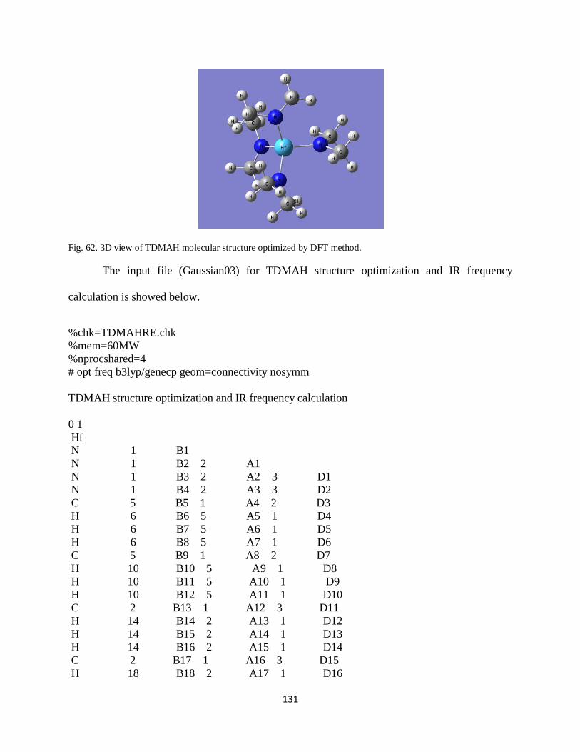
131
Fig. 62. 3D view of TDMAH molecular structure optimized by DFT method.
The input file (Gaussian03) for TDMAH structure optimization and IR frequency
calculation is showed below.
%chk=TDMAHRE.chk
%mem=60MW
%nprocshared=4
# opt freq b3lyp/genecp geom=connectivity nosymm
TDMAH structure optimization and IR frequency calculation
0 1
Hf
N 1 B1
N 1 B2 2 A1
N 1 B3 2 A2 3 D1
N 1 B4 2 A3 3 D2
C 5 B5 1 A4 2 D3
H 6 B6 5 A5 1 D4
H 6 B7 5 A6 1 D5
H 6 B8 5 A7 1 D6
C 5 B9 1 A8 2 D7
H 10 B10 5 A9 1 D8
H 10 B11 5 A10 1 D9
H 10 B12 5 A11 1 D10
C 2 B13 1 A12 3 D11
H 14 B14 2 A13 1 D12
H 14 B15 2 A14 1 D13
H 14 B16 2 A15 1 D14
C 2 B17 1 A16 3 D15
H 18 B18 2 A17 1 D16

132
H 18 B19 2 A18 1 D17
H 18 B20 2 A19 1 D18
C 4 B21 1 A20 2 D19
H 22 B22 4 A21 1 D20
H 22 B23 4 A22 1 D21
H 22 B24 4 A23 1 D22
C 4 B25 1 A24 2 D23
H 26 B26 4 A25 1 D24
H 26 B27 4 A26 1 D25
H 26 B28 4 A27 1 D26
C 3 B29 1 A28 2 D27
H 30 B30 3 A29 1 D28
H 30 B31 3 A30 1 D29
H 30 B32 3 A31 1 D30
C 3 B33 1 A32 2 D31
H 34 B34 3 A33 1 D32
H 34 B35 3 A34 1 D33
H 34 B36 3 A35 1 D34
B1 2.14000000
B2 2.14000000
B3 2.14000000
B4 2.14000000
B5 1.47000000
B6 1.07000000
B7 1.07000000
B8 1.07000000
B9 1.47000000
B10 1.07000000
B11 1.07000000
B12 1.07000000
B13 1.47000000
B14 1.07000000
B15 1.07000000
B16 1.07000000
B17 1.47000000
B18 1.07000000
B19 1.07000000
B20 1.07000000
B21 1.47000000
B22 1.07000000
B23 1.07000000
B24 1.07000000
B25 1.47000000
B26 1.07000000
B27 1.07000000
A11 109.47123134
A12 109.47120255
A13 109.47120255
A14 109.47120255
A15 109.47123134
A16 109.47120255
A17 109.47120255
A18 109.47120255
A19 109.47123134
A20 109.47120255
A21 109.47120255
A22 109.47120255
A23 109.47123134
A24 109.47120255
A25 109.47120255
A26 109.47120255
A27 109.47123134
A28 109.47120255
A29 109.47120255
A30 109.47120255
A31 109.47123134
A32 109.47120255
A33 109.47120255
A34 109.47120255
A35 109.47123134
D1 119.99998297
D2 -120.00003407
D3 -59.67581539
D4 179.42741141
D5 -60.57257380
D6 59.42741881
D7 60.32419940
D8 59.78081838
D9 179.78083317
133
B28 1.07000000
B29 1.47000000
B30 1.07000000
B31 1.07000000
B32 1.07000000
B33 1.47000000
B34 1.07000000
B35 1.07000000
B36 1.07000000
A1 109.47121829
A2 109.47123134
A3 109.47121829
A4 109.47120255
A5 109.47120255
A6 109.47120255
A7 109.47123134
A8 109.47120255
A9 109.47120255
A10 109.47120255
D22 57.63966610
D23 53.51145130
D24 66.14384390
D25 -173.85614130
D26 -53.85614870
D27 -119.99798461
D28 67.09960684
D29 -172.90037837
D30 -52.90038577
D31 120.00200060
D32 65.84469999
D33 -174.15528521
D34 -54.15529261
Hf 0
LANL2DZ
****
H C N 0
6-31+G(d,p)
****
Hf 0
LANL2DZ
D3 -59.67581539
D4 179.42741141
D5 -60.57257380
D6 59.42741881
D7 60.32419940
D8 59.78081838
D9 179.78083317
D10 -60.21917422
D11 59.88892443
D12 69.90242347
D13 -170.09756173
D14 -50.09756913
D15 -60.11109036
D16 -179.68318452
D17 -59.68316972
D18 60.31682288
D19 173.51146610
D20 177.63965870
D21 -62.36032651