chemical vapor deposition thin films as biopassivation
TRANSCRIPT

Chemical Vapor Deposition Thin Films asBiopassivation Coatings and Directly Patternable Dielectrics
by
Hilton G. Pryce Lewis
M.S. in Chemical Engineering PracticeMassachusetts Institute of Technology, 1998
B. Sc. Eng. (Chemical)University of Natal, South Africa, 1995
Submitted to the Department of Chemical Engineeringin Partial Fulfillment of the Requirements for the Degree of
DOCTOR OF PHILOSOPHY IN CHEMICAL ENGINEERINGAT THE
MASSACHUSETTS INSTITUTE OF TECHNOLOGY
June 2001
© 2001 Massachusetts Institute of Technology. All rights reserved.
Signature of Author ............ ...... ........................................Department of Chemical Engineering
April 27, 2001
C ertified by .............................. .. ....... .... ......... . .... ..
~~~~/ ~Karen K. GleasonProfessor of Chemical Engineering
, Thesis Supervisor
Accepted by ......... ...............................Robert E. Cohen
St. Laurent lrotessor ot nemical EngmeermgChairman, Committee for Graduate Students
tuiiHiVES

Chemical Vapor Deposition Thin Films asBiopassivation Coatings and Directly Patternable Dielectrics
by
Hilton Gavin Pryce Lewis
Submitted to the Department of Chemical Engineeringon April 27, 2001 in Partial Fulfillment of the
Requirements for the Degree ofDoctor of Philosophy in Chemical Engineering
ABSTRACT
Organosilicon thin films deposited by pulsed plasma-enhanced chemical vapordeposition (PPECVD) and hot-filament chemical vapor deposition (HFCVD) wereinvestigated as potential biopassivation coatings for neural probes. It was found thatorganosilicon films from identical precursors differ in structure according to the methodof deposition. For films produced from the cyclic siloxane precursor,hexamethylcyclotrisiloxane, pulsed plasma excitation reduced crosslink density overcontinuous excitation and produced flexible films resistant to prolonged saline soaktesting. Deposition via a thermal process, HFCVD, allowed films of novel organosiliconstructure to be formed from both hexamethylcyclotrisiloxane and its eight-memberedanalog, octamethylcyclotetrasiloxane. Characterization of these films was accomplished,and the effect of filament temperature on the chemical structure was elucidated. Silicon-silicon bonding and the retention of ring structures from the precursor was observed inHFCVD organosilicon films using Micro-Raman spectroscopy.
A direct dielectric patterning process was proposed for semiconductor manufacturing.In this process, a dielectric material is patterned directly and developed without theneed for a sacrificial photoresist layer. HFCVD fluorocarbon films are underconsideration as low-dielectric constant interlayer dielectrics, and direct patterning ofthese materials was demonstrated using e-beam irradiation and supercritical CO2development. The use of a gas-phase initiator species for HFCVD of fluorocarbon thinfilms was also demonstrated. Initiation enhanced deposition rates significantly andprovided a means of selectively end-capping polymer chains present in the filmstructure.
Thesis Supervisor: Karen K. GleasonTitle: Professor of Chemical Engineering
2

For Mom and Dad
3

Acknowledgments
I dedicate this work to Mom and Dad. I would be nowhere without theirunconditional love and support. They have always been role models for me inhow to inspire and encourage selflessly; pulling rather than pushing. I want tothank them for everything they have given me, and tell them I love them. I alsowant to acknowledge my family back in South Africa: Jord, Trish, Sue, Ray,Cameron, Dylan, Judith, Sonny, and - of course - Ang in jolly old England. Littledid I know five years could be so happy and sad at the same time. Also, to thememory of Gaga and Granny; I'm so glad I got to share in your lives for most ofmine. Love you lots, miss you more.
It has been the utmost privilege for me to have worked closely with myadvisor, Karen, during my time here. I made a very, very good choice, and it'stough to believe now that I almost wrote off the whole Ph.D. thing. Yourguidance, diplomacy, and friendship is much appreciated, and will hopefullycontinue for many years to come. A stellar advisor begets a stellar researchgroup, and I want to acknowledge the many witty, brilliant, sour, garrulous,overly fastidious, laconic, and plain old friendly personalities that have passedthrough the group over the years. Keep 'em coming! I want to especially thankKen for many years of lengthy and enlightening conversation (animated on mypart, incisive on his) and friendship. Many more to come, I hope. I'd also like tothank my "summer students", Tom and Jeff, who I credit with advancing myaccomplishments in two giant leaps. Finally, I'd like to thank Todd Bailey for hiswarm interaction and fantastic parties!
Many friends have been made (and a few lost, unfortunately) during mytime in Boston. Thanks to all those people who made my Ph.D. such fun. Specialthanks to Inge and Bruno - you intimidating Europeans! You make things somuch brighter and sunnier, and I relish the years we have together both in thepast and to come. And, yes, Inge; Wendy and I will still talk to you...
My degree is in two parts: BW and AW. I am sure that everything I wroteafter meeting you, Wendy, is that much more eloquent and cheery. I had to go along way, and wait a long time, but I found you. Now we sit back and enjoy theride. I love you, and can't wait for our new life together.
Finally, I want to acknowledge my Lord, Jesus Christ. Thank You for allthat You've given me.
"But they that wait upon the Lord shall renew their strength; they shallmount up with wings as eagles; they shall run, and not be weary; they shallwalk, and not faint." Isaiah 40:31.
4
Table of Contents
Abstract 2Dedication 3Acknowledgments 4List of Figures 7List of Tables 12List of Notations 13
CHAPTER 1 14Introduction
1.1 Chemical Vapor Deposition (CVD) 151.2 Biopassivation Coatings 181.3 Directly Patternable Dielectrics 231.4 Scope of Thesis 251.5 References 25
CHAPTER 2 30Pulsed-PECVD Films from D3 for Use as Insulating Biomaterials
2.1 Abstract 312.2 Introduction 322.3 Experimental 342.4 Results and Discussion 352.5 Conclusions 462.6 References 47
CHAPTER 3 50HFCVD of Organosilicon Thin Films from D3 and D4
3.1 Abstract 513.2 Introduction 523.3 Experimental 533.4 Results and Discussion 543.5 Conclusions 753.6 References 75
CHAPTER 4 79E-Beam Patterning of HFCVD Fluorocarbon Films Using Supercritical CO2 as Developer
4.1 Abstract 804.2 Introduction 814.3 Experimental 824.4 Results and Discussion 834.5 Conclusion 864.6 References 86
5

CHAPTER 5 88Perfluorooctane Sulfonyl Fluoride as an Initiator in HFCVD of Fluorocarbon Thin Films
5.1 Abstract 895.2 Introduction 905.3 Experimental 915.4 Results and Discussion 925.5 Conclusions 995.6 References 99
CHAPTER 6 101Hot-Wire Deposition of Organosilicon and Fluorocarbon Thin Films
6.1 Abstract 1026.2 Introduction 1036.3 Experimental 1036.4 Results and Discussion 1056.5 Conclusions 1096.6 References 109
CHAPTER 7 111Conclusions and Future Work
7.1 Conclusions 1127.2 Future Work 1147.3 References 114
APPENDIX A 115Reactor Design and Construction
A.1 Description 116A.2 Main Chamber CAD Drawings 118A.3 Bottom Plate CAD Drawing 121A.4 Reactor Lid CAD Drawings 121A.5 Rear Flange CAD Drawings 123
APPENDIX B 124Additive Precursors Used in Combination with HFPO HFCVD
B.1 List of Additive Precursors 125B.2 Deposition Rates with Additive Precursors 125B.3 New Chemistries Possible Using HFCVD with Dual Precursors 126
6

List of Figures
CHAPTER ONE
Figure 1-1. Schematic of a typical parallel-plate PECVD system.
Figure 1-2. Potential problem areas in the protection of implantable integrated circuitsby tnin layers of insulating hiomaterials.
Figure 1-3. Direct dielectric patterning scheme.
CHAPTER TWO
Figure 2-1.
Figure 2-2.
Figure 2-3.
Figure 2-4.
Figure 2-5.
Figure 2-6.
Figure 2-7.
Optical micrographs showing 750 m loops of 3-mil copper wire coatedwith D pulsed-PECVD film at (a) CW, (b) 10/60, (c) 50/300, and (d)100/600. Film thickness is (a) 19 m, (b) 9 um, (c) 12 m, and (d) 13 pm.Film deposited at 100/600 shows the most flexibility.
Coating on a University of Michigan probe deposited at 50/300, showingcvnformity of coating. Film is 20 pgm at the thickest point.
FTIR spectra of (a) pulsed-PECVD film deposited at 100/600, and (b)PDMS secondary standard. Absorption spectra of pulsed-PECVD filmnhas been normalized to standard thickness of 1,500 A.
FTIR spectral region from 600 cm-' to 1,500 cm-' for CW, 100/600 and10/400 films. Respective duty cycles are 100%, 14% and 2.4%.
FTIR spectral region from 3,050 cm-' to 2,800 cm-' for CW, 100/600 and10/400 films, showing CHx correlated absorptions.
Possible crosslinking and/or branching nodes present in PECVD films.Non-branching M and D groups are shown for reference. Nodes of Type Iinvolve only oxygen, while nodes of Type H involve both oxygen atomsand methylene groups.
Reaction pathways for the production of polymerization precursors fromD 3.
CHAPTER THREE
Figure 3-1.
Figure 3-2.
Arrhenius plot of D3 and D4 films produced by HFCVD. Straight lineswere fitted by regression.
FTIR spectra of a. D3 PECVD film deposited under continuous-waveexcitation, and b. D3 HFCVD film deposited at 1000°C.
7

Figure 3-3.
Figure 3-4.
FTIR spectra of D3 HFCVD films deposited at filament temperatures of a.860°C, b. 000°C, and c. 100°C.
FTIR spectra of D 4 HFCVD films deposited at filament temperatures of a.800°C, b. 900°C, and c. 1000°C.
Figure 3-5.
Figure 3-6.
Figure 3-7.
Figure 3-8.
Figure 3-9.
Micro-Raman spectra of a. D3, b. D4, c. PDMS, d.deposited at a filament temperature of 1000°C, and e.deposited at a filament temperature of 1100°C.
Micro-Raman spectra of D3 HFCVD filmstemperatures of 860°C, 1000°C, and I 100(C.
Micro-Raman spectra of D4 HFCVD filmstemperatures of 800°C, 900°C, and 1000°C.
D4 HFCVD filmD3 HFCVD film
deposited
deposited
29Si Solid-State CP-MAS NMR spectra of D3 HFCVD filmfilament temperatures of 860°C, 1000°C, and 1100°C.
29Si Solid-State CP-MAS NMR spectra of D4 HFCVD filmfilament temperatures of 800°C, 900°C, and 1000°C.
at filament
at filament
deposited at
deposited at
Figure 3-10.
Figure 3-11.
Atomic force micrograph of D4 HFCVD film deposited at a filamenttemperature of 900°C. RMS roughness over image area is 1.1 nm. RMSroughness of bare silicon is 0.53 nm.
Reaction pathways for the production of polymerization precursor speciesin D3 and D4 HFCVD.
CHAPTER FOUR
Figure 4-1.
Figure 4-2.
Figure 4-3.
FTIR spectra of hot-filament CVD fluorocarbon films fromshowing the change in -OH and -COOH content as a result ofprocess conditions. OH/CF2 ratios were estimated by integratingof each absorption stretch in the FTIR spectra.
HFPO,varying
the area
Contrast curves of samples 3, 4, 6, and 7, showing e-beam sensitivityfollowing SCF CO2 development. Sample 4 developed completely inpositive-tone.
AFM image of 1.0 gtm lines/spaces in sample 5. Left image is a top-downview, right plot is a cross-section through the line shown at left.
CHAPTER FIVE
8

Figure 5-1.
Figure 5-2.
Figure 5-3.
Figure 5-4.
Deposition rates of HFCVD fluorocarbon films from PFOSF and HFPO.showing the effect of a. adding PFOSF, and b. changing filamenttemperature. Trend lines in Figure 5-la are included for visualclarification. Figure 5-lb shows data for PFOSF/HFPO ratios greater than0.07, and is plotted in Arrhenius form. Regression fits illustrate kineticregimes above and below -470°C.
Nuclear Magnetic Resonance (NMR) spectra of a. HFCVD film from theprecursors HFPO and PFOSF, b. HFCVD film from the precursor HFPOwith no PFOSF, and c. bulk PTFE. Concentrations of CF3, CF2, and CFare shown in mol %.
Atomic Force micrographs showing the effect of filament temperature onthe morphology of HFCVD films from HFPO and PFOSF. Films weredeposited at a PFOSF/HFPO ratio of 0.145 and filament temperatures of a.435°C, b. 510°C, and c. 580°C. RMS roughnesses are also shown.
Proposed polymerization mechanism for HFCVD using HFPO andPFOSF.
CHAPTER SIX
Figure 6-1.
Figure 6-2.
Figure 6-3.
Figure 6-4.
Figure 6-5.
Figure 6-6.
Figure 6-7.
Schematic of the HWCVD Chamber. Showing gas inlet through uppershowerhead, pyrolysis on square filament array, and deposition onto awafer substrate resting on the bottom electrode. Gas pump out is towardthe back side of the chamber.
Solid state 9F NMR of HWCVD fluorocarbon film (bottom) and PTFE(top).
FTIR of HWCVD fluorocarbon film (bottom) and PTFE (top).
Reactions for the pyrolysis of HFPO and polymerization ofdifluorocarbene.
FTIR of HWCVD organosilicon film (top) and PDMS (bottom).
HWCVD fluorocarbon low dielectric constant film directly patterned at1.0 (left) and 0.25 (right) micron resolution.
Scanning electron micrograph of HWCVD porous fluorocarbon film at theedge of the silicon wafer substrate (bottom right). The tilt angle makes itpossible to observe both the surface morphology (top left) and porositythrough the thickness of the layer.
CHAPTER SEVEN
9
__

Figure 7-1. Compositional space available from CVD of organosilicon andfluorocarbon materials, as derived from 29Si and 9F NMR. This workfillkdi in the top row of the matrix, and furthered our understanding offluorocarbon HFCVD chemistry.
APPENDIX
Figure A-1.
Figure A-2.
Figure A-3.
Figure A-4.
Figure A-5.
Figure A-6.
Figure A-7.
Figure A-8.
Figure A-9.
Figure A-10.
Figure A-l 1.
Figure
Figure
Figure
Figure
A-12.
A-13.
A-14.
A-15.
A
Photographs of the dual-mode CVD reactor system known as Pumpkin.
Front and rear view of chamber, showing feed port and pumping port.
Top view of chamber, showing lid design, and filament orientation forHFCVD.
Side view of chamber, showing water-cooled stage, pumping port andaccess door.
Front view of chamber design.
Front vie of chamber design, rotated 30 ° clockwise as observed fromabove.
Front view of chamber design, rotated 60° clockwise as observed fromabove.
Front view of chamber design, rotated 90° clockwise as observed fromabove.
Top view of chamber design, showing position of ports.
Assembly view of main chamber design.
Side cutaway view of original design of bottom plate. Note that coppertubing was replaced with a stainless steel reservoir -in. deep with inletand outlet tubing in final construction.
Side view of reactor lid, showing /4-in. VCR and NW 16 ports.
Side cutaway view of reactor lid, showing 1/2-in. o-ring port and NW16ports.
Top view of reactor lid, showing all ports.
Top and side views of rear flange.
10

APPENDIX B
Figure B-1.
Figure B-2.
Typical deposition rates obtained using HFPO with secondary precursorspecies.
Cls XPS spectra showing high surface concentrations of terminal CH 3
groups in PTFE films.
11

List of Tables
CHAPTER ONE
Table 1-1. Previous investigations of CW PECVD with organosilicon monomers.
CHAPTER TWO
Table 2-1.
Table 2-2.
Table 2-3.
CHAPTER
Table 3-1.
Table 3-2.
Table 3-3.
Table 3-4.
Table 3-5.
CHAPTER
Table 4-1.
CHAPTER
Table 6-1.
CHAPTER
Table 7-1.
APPENDIX
Table B-1.
Results of wire coatings on 3-mil copper wire deposited from D3 usingpulsed-PECVD.
Results of saline soak testing of pulsed-PECVD films deposited under avariety of pulse conditions.
FTIR assignments from the literature.
THREE
FTIR assignments from the literature.
Raman assignments from the literature.
Raman siloxane symmetric stretching mode (SSM) assignments forvarious chemical environments.
29Si NMR structures and chemical shifts commonly observed inorganosilicon CVD films.
XPS elemental ratios for HFCVD films from D 3 and D4.
FOUR
Deposition conditions for CVD films that showed sensitivity to e-beamexposure.
SIX
Typical process conditions for HWCVD.
SEVEN
Silicon bonding environments in PPECVD and HFCVD organosiliconfilms.
'B
IPrecursors used in combination with HFPO HFCVD.
12

List of Notations
K dielectric constantAFM atomic force microscopyCP cross polarizationCP-MAS cross polarization with magic angle spinningCVD chemical vapor depositionCW continuous-wave plasma-enhanced chemical vapor depositionD3 hexamethylcyclotrisiloxaneD4 octamethylcyclotetrasiloxaneEBDW e-beam direct write lithographyEPL e-beam projection lithographyESH environment, safety and healthESR electron spin resonance spectroscopyFTIR Fourier transform infrared spectroscopyHFCVD hot-filament chemical vapor depositionHFPO hexafluoropropylene oxideHMDSO hexamethyldisiloxaneIC integrated circuitILD interlayer dielectricITRS International Technology Roadmap for SemiconductorsMAS magic angle spinningMW molecular weightNMR nuclear magnetic resonanceOM optical microscopyOSG organosilicate glassPDMS polydimethylsiloxanePECVD plasma enhanced chemical vapor depositionPFOSF perfluorooctane sulfonyl fluoridePPECVD pulsed plasma enhanced chemical vapor depositionPTFE poly(tetrafluoroethylene)RF radio-frequencySCF supercritical fluidSEM scanning electron microscopeTMS tetramethylsilaneUV ultravioletVTMS vinyltrimethylsilaneXPS x-ray photoelectron spectroscopy
13

CHAPTER IIntroduction
14
X h
= Z- - 1 1---- L-'c---
I
I
iI
I
1;
I;,1,

1.1 Chemical Vapor Deposition (CVD)
CVD is a vacuum technology capable of producing thin, pinhole-free films on
substrates of complex geometry.1-3 In conventional, or thermal, CVD deposition takes
place on a heated susceptor and substrate and the technique is most often used to produce
inorganic materials such as SiO2. Only in a few cases is it possible to produce organic
thin films, due to their poor thermal stability and adsorption-dominated kinetics.3 For
organic materials, a CVD process is required in which reactive species are generated in
the gas phase and film growth proceeds via recombination on a cooled substrate. The
method of activation to produce film growth precursors is thus a key differentiator in
CVD of these types of materials. In this work, we have used both electrical (PECVD and
PPECVD) and thermal activation (HFCVD).
Plasma-Enhanced Chemical Vapor Deposition (PECVD)
PECVD involves the formation of thin films on surfaces from a vapor phase
precursor under the influence of a plasma (or glow discharge).4 " The plasma is a
partially ionized gas usually formed by exposing a gaseous precursor to an electrical field
at low pressure (<10 Torr). It consists of electrons, ions, free radicals, molecules in
excited states, and photons of various energies. Plasmas used for etching and deposition,
generally called "cold plasmas", are in a non-equilibrium state wherein the temperature of
the electrons is much higher than that of the gas molecules. As a result, the temperature
of the gas molecules is close to ambient and plasma chemistry can occur without thermal
degradation of reactants and products. Plasma polymerization is a specific type of plasma
chemistry which involves reactions between plasma species, between plasma and surface
species, and between surface species. Reactive species are generated in the plasma by
electron impact collisions, and thus overcome kinetic limitations that may exist in
thermally activated processes. This allows monomers to be used that would not
polymerize under conditions of conventional molecular addition polymerization, such as
saturated alkanes or benzene. Plasma films are deposited on surfaces contacting the
plasma of a precursor gas in the form of a thin film and/or powder. The discharge also
supplies energetic radiation (e.g. positive ions and photons) that bombards surfaces
exposed to the plasma. This alters the surface chemistry during deposition, and can result
15

in competitive ablation or etching of the growing film. Using PECVD, ultrathin, pinhole-
free films that are highly coherent and adherent to a variety of substrates may be prepared
from monomers not polymerizable by conventional means. Films are generally
chemically inert, insoluble, mechanically tough, thermally stable and have been used or
considered for a wide variety of electrical 12 16, optical 1' 1 7 -2 2 and biomedical6 9' 23-37
applications, and as permselective membranes 24' 38 42 and protective coatings 20.43-45
POWER SUPPLY
Powewith
Substrate
Viewport
GroundecElectrode
Water In - Water Out - Ground
Figure 1-1. Schematic of a typical parallel-plate PECVD system.
A typical parallel plate plasma reactor system is shown in Figure 1-1. It consists
of a deposition chamber with two electrodes located parallel to each other, a power
generator, an impedance matching network and a vacuum pumping system. Radio-
frequency (RF) power of 13.56 MHz is supplied to the top, or powered, electrode from an
RF generator via the impedance matching network. The purpose of the matching network
is to balance the impedance of the generator with that of the discharge, thereby
maximizing power transfer to the discharge. In PECVD, substrates are usually placed on
the bottom electrode, which is grounded and cooled. Discharge is normally confined to
the space between the two electrodes. The primary process variables of consideration are
the flow rate of the precursor gas, system pressure, RF discharge power and substrate
temperature. The flow rate of feed gas and the system pressure determine the residence
time of the monomer in the reactor. System pressure also determines the mean free path
16

length of species in the plasma, while the discharge power affects the degree of ionization
in the plasma and the extent of monomer fragmentation. Substrate temperature affects
adsorption and desorption kinetics and surface mobility of precursor species on the
substrate surface.
Unlike conventional polymers, plasma films often have only limited polymeric
character, and tend to form irregular three-dimensional crosslinked networks. UV
irradiation and ion bombardment of the growing film, as well as the mechanism of
plasma film growth itself, can result in the formation of trapped free radicals, or dangling
bonds, in the film46-4 8. Upon exposure to atmosphere, these dangling bonds are oxidized,
leading to concomitant changes in film structure and properties. This aging characteristic
of plasma films makes them undesirable for use in some applications, particularly where
electrical insulation is a requirement. The effect of ion bombardment is also to increase
the crosslink density in plasma films, which often results in brittle, inflexible films.
Pulsed Plasma-Enhanced Chemical Vapor Deposition (PPECVD)
A promising method that has been applied in an effort to reduce dangling bond
concentrations and crosslinking in plasma films is pulsed-PECVD, or PPECVD.-24 37 4649-
62 In this technique, RF excitation is modulated on and off. When the RF power is on,
both ions and reactive neutrals are produced in the gas phase. However, ions often have
much shorter lifetimes than neutrals and the ratio of neutrals to ions increases during the
period when RF power is off. 51' 52,54,63 '65 Film deposition from reactive neutrals will thus
be favored and the decrease in ion bombardment during the off period is anticipated to
lead to a reduction in the number of dangling bonds and crosslinks.
Investigation of PPECVD using fluorocarbon precursors has been shown to
produce flexible, conformal fluorocarbon films with reduced dangling bond concentration
and lower crosslink density as compared to films obtained using continuous-
PECVD 55 58'60 '6 1. One of the goals of this project was to extend the PPECVD technique to
organosilicon precursors, specifically the cyclic siloxane hexamethylcyclotrisiloxane
(D 3). Coatings produced in this way were to be evaluated as potential encapsulant
materials for biopassivation of neural probe devices.
17

Hot-Filament CVD (HFCVD)
In contrast to PECVD and PPECVD, HFCVD (also called pyrolytic CVD)
generates reactive species through thermal activation at a hot surface - typically a heated
wire. HFCVD has been used extensively in the deposition of diamond thin films66 6 7, but
has only recently been extended to polymer systems by our group.6061' 68,69 The substrate
is cooled as in PECVD, but the lack of ion bombardment, UV, and electron irradiation in
the non-plasma environment alters the chemistry of the growth process and limits the
number of reaction pathways available for film growth. This makes it possible, for
instance, to produce films that are spectroscopically indistinguishable from PTFE
(commonly known as Teflon TM).60 6 1'68 Using the same precursor, hexafluoropropylene
oxide (HFPO), in a PECVD process results in films in which carbon is present in a
variety of bonding environments ranging from CF3 to completely defluorinated
quaternary carbon. 48 53' 58.6070
Much work has been done in characterizing fluorocarbon films produced using
this method and understanding the chemistry of the HFCVD process with HFPO.60 '61'68'71 -
73 At the start of this project, however, only preliminary work had been done in extending
the HFCVD technique to organosilicon precursors. 69 One of the primary goals of this
work was thus to elucidate the chemistry of the process and rigorously characterize these
organosilicon materials. In particular, we wanted to compare and contrast organosilicon
materials deposited from similar precursors using PPECVD and HFCVD
1.2 Biopassivation Coatings
Challenges for the Encapsulation of Implantable Devices
When a foreign object contacts blood or tissue fluids in the environment of the
body, it is the surface of the object that the fluids first encounter. The immediate
physiological response after exposure is usually the adsorption of biomolecules,
particularly proteins. The chemical composition, topology, and morphology of this
surface is thus extremely important in mediating the biologic response of the body to
implantable devices of any kind. A coating of a biocompatible material on a biomedical
device is a powerful method for altering the surface properties of the device without
changing the bulk properties. Such a material can also serve to insulate and protect the
18
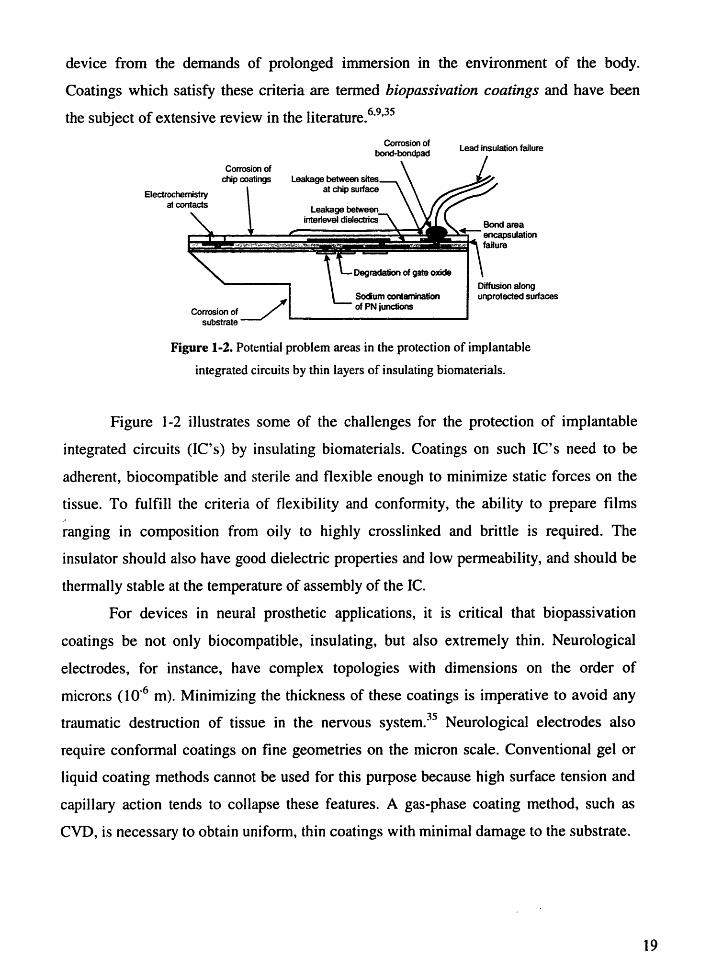
device from the demands of prolonged immersion in the environment of the body.
Coatings which satisfy these criteria are termed biopassivation coatings and have been
the subject of extensive review in the literature.6 ' 9' 3 5
Corrosion ofhnnrho nnrl Lead insulation failure
Electrocheiat co
SUOSIrale
Figure 1-2. Potential problem areas in the protection of implantable
integrated circuits by thin layers of insulating biomaterials.
Figure 1-2 illustrates some of the challenges for the protection of implantable
integrated circuits (IC's) by insulating biomaterials. Coatings on such IC's need to be
adherent, biocompatible and sterile and flexible enough to minimize static forces on the
tissue. To fulfill the criteria of flexibility and conformity, the ability to prepare films
ranging in composition from oily to highly crosslinked and brittle is required. The
insulator should also have good dielectric properties and low permeability, and should be
thermally stable at the temperature of assembly of the IC.
For devices in neural prosthetic applications, it is critical that biopassivation
coatings be not only biocompatible, insulating, but also extremely thin. Neurological
electrodes, for instance, have complex topologies with dimensions on the order of
microns (10-6 m). Minimizing the thickness of these coatings is imperative to avoid any
traumatic destruction of tissue in the nervous system. Neurological electrodes also
require conformal coatings on fine geometries on the micron scale. Conventional gel or
liquid coating methods cannot be used for this purpose because high surface tension and
capillary action tends to collapse these features. A gas-phase coating method, such as
CVD, is necessary to obtain uniform, thin coatings with minimal damage to the substrate.
19

Organosilicon Thin Films as Biopassivation Coatings
Both PPECVD and HFCVD show promise as methods to tailor the composition
of films to meet the foregoing criteria. In particular, organosilicon thin films deposited
using these techniques are exciting candidates for biopassivation coatings. Previous work
has confirmed their suitability as biocompatible materials.
Chawla investigated plasma-deposited films of D 3 and D 4 on Celgard®-2400 and
Silastic® membranes and evaluated the adhesion of platelets and leucocytes using an in
vitro loop25 and an ex vivo shunt system with a canine model2 5 29. It was determined that
the number of platelets and leukocytes adhering to the silicone coated samples were less
than on the untreated controls. Ishikawa et al. examined a number of organosilicon
monomers, including D3, and found that the number of platelets adhering to coated glass
slides and the ATP released from these platelets in a human blood in vitro system was 10-
30% less than the uncoated slides31. Hasirci investigated the deposition of HMDSO on
activated charcoal, used in hemoperfusion, by PECVD. It was found that the silicone
coating significantly reduced damage from the charcoal granules to platelets, erthrocytes
and leucocytes in sheep's blood, without substantially reducing the absorptive capacity of
the charcoal 32. Cannon et al. detail the synthesis of a fine neurological electrode
consisting of W-26 at.% Re wire coated with plasma-polymerized HMDSN. No in vivo
biocompatibility and stability studies were reported, and some problems were
experienced obtaining smooth pinhole-free coverage of the substrate27 . No subsequent
work on this topic has been published by this group. More recently, Nichols reported the
synthesis of a novel polymeric material, Plasmalene®, as an hermetic coating on wire
substrates. The polymer coatings were deposited by vacuum processes which included
PECVD and thermal vapor deposition of methane and xylylene 7 4. Finally, Lin et al. have
coated the inner surface of low-density polyethylene (LDPE) tubing with plasma-
polymerized HMDSO and ammonia for possible use as an artificial blood vessel34.
20

Table 1-1. Previous investigations of CW PECVD with organosilicon monomers.
Precursor Structural Formula Ref.cH,
Tetramethylsilane I 75-78,C-- S--CH,(TMS) H I
CH3
CH,Vinyltrimethylsilane C17.46.77.79
HexaCethyldisiloxane H--CH =CH,(VTMS) CH,
(HMDSO) HCi --CH, CH,
CH3 C1 CHOI
Tetramethyl- 1,3-bis(chloromethyl)-disiloxane I I 82
CH, CH,
(CH),OH (CH),OH
Tetramethyl- 1 ,3-bis(hydroxylbutyl)-disiloxane I I 82H3C--- O--Si--CH3I I
CH, CH,
(CH,),NH, (CH3 NH,
Tetramethyl- 1,3-bis(amino propyl)disiloxane I I 82H30 - Si - - Si - CH.
CH, CH,
CH=CH CH CH,
Divinyltetramethyldisiloxane i I 87,91H,C -i- 0-- -- cH,
CH. CH,
CH, H,
Hexamethylcyclotrisiloxane 0 oSi 24.25,29.92-94
(D3) H,C I I CH,
CH, / \
CH,
' H3C S \ -H 3
Octamethylcyclotetrasiloxane . j-o CH 12,24.78,87.89,93,94
(D4) H
CH3 ?Lf' CH 3
CH3
CCH H2C-HZCFJ
2,4,6-Tris (3,3,3-trifluoropropyl) methyl S 75.95
cyclotrisiloxane H3C I I-
CF,HCH, CH,CHFCF
CH3 CH,
Hexamethyldisilazane I I 27,75,76,91.94,96HC --SI-- NH--Si-- CH3
C__ C'_ _
Wr6bel and Wertheimer give an excellent overview of the literature on plasma
deposition of organosilicon materials' 3. CW PECVD has been investigated using a wide
variety of monomers. Table 1-1 lists some of this work. In contrast, PPECVD has been
investigated by only a few workers and in limited detail24' 25' 29 46'97, and no previous work
using a technique like HFCVD has been reported for any organosilicon precursors. Using
21

PPECVD, Yasuda et al. tested the monomers hexamethyldisilane (HMDS),
tetramethyldisiloxane (TMDSO), hexamethyldisiloxane (HMDSO) and
divinyltetramethyldisiloxane (DVTMDSO) with a 0. ms on/ 0.9ms off pulse program in
an electrodeless inductively-coupled plasma reactor. Results from electron spin resonance
(ESR) spectroscopy indicated that the concentration of trapped free radicals in pulsed
plasma polymers was significantly lower than that in continuous plasma polymers for all
of the organosilicon monomers.46 In other work using PPECVD, Chawla used
hexamethylcyclotrisiloxane (D 3) and octamethylcyclotetrasiloxane (D 4) to prepare
silicone coated membranes for possible use as blood oxygenators. Though it is not clearly
described in his publications, Chawla used 30W pulsed RF power of 66ms on/66 ms off
in a capacitively-coupled tubular reactor. According to Sipehia, this duty cycle was
chosen to prevent excessive crosslinking in the film 98. None of these publications,
however, analyzed the effect of the duty cycle on the structure and properties of the films.
Only Panchalingam et al. used vinyltrimethylsilane (VTMS) to investigate the effect of
systematic variations in the duty cycle on the chemistry and deposition rates of pulsed
plasma films. Hence, there was considerable scope for further investigation in using
PPECVD to produce organosilicon films with desirable and tunable properties.
The goal of this portion of the project was thus to investigate deposition of
organosilicon thin films by PPECVD and HFCVD, with particular application to the
coating of neurological electrodes and other implantable devices. It was desired to obtain
films that had properties superior to their CW-PECVD counterparts, such as high
deposition rates (>1000 A/min), polymeric structure, low defect density, resistance to
prolonged immersion in solution, and flexibility sufficient to resist cracking under stress.
Examples of defects included non-uniformities in the film such as columnar structures,
included contaminant particles, high dangling bond concentrations and excessive
crosslinking. Thermal stability, good adhesion, and uniformity over non-planar substrates
were also desirable properties. It was also important to understand the structure-property-
processing relationship in the CVD process, and to determine the importance and effect
of process variables on film chemistry.
22

1.3 Directly Patternable Dielectrics
Thin films produced by HFCVD and PPECVD also show promise as materials
capable of undergoing patterning by lithographic means.76 '91 99 'I In this portion of the
project, we consider the use of fluorocarbon and organosilicon films deposited by
HFCVD for producing nanometer-scale features in microelectronics manufacture. Both
fluorine- and silicon- containing polymeric materials are under consideration as
candidates in next-generation patterning technologies, such as 157 nm photolithography
and e-beam projection lithography (EPL, e.g. SCALPEL, PREVAIL).'07, 109 Their
transparency makes them ideal resist candidates for 157-nm lithography' 0 7, and their low
dielectric constant makes them strong contenders as interconnect materials'4.
Direct Dielectric Patterning Process
0 0
00 .0 BS.5 ..
*6 - I
dielectricdeposition
spin-onimaging layer
selectivei rrad iation
development inaqueous base
dielectricpatterning
imaginglayer strip
*L11,'1 wet chemistry elimina
cvd of piatternabledietectric layer
ted
selectiveirradiation
I1d in" wet chemistry eliminated
developrment insupercritical CO,(SC F CO,)
Figure 1-3. Direct dielectric patterning scheme.
The objective of this work - a collaboration between MIT and Cornell University
- is thus to merge the role of resist and low-k dielectric. Specifically, we propose a direct
dielectric patterning process in which a material is deposited by CVD, exposed, and
developed using no wet chemistry, as illustrated in Figure 1-3.
23

In this process, an irradiation-sensitive CVD film is exposed using e-beam or a
157-nm source, and developed using supercritical CO2 as a dry developing medium. The
patterned film then serves as a low-k interconnect material. This technology would
greatly simplify future device manufacture by reducing the number of steps involved in
patterning. Supercritical CO2 also offers many processing advantages over wet
development, including improved resolution and the prevention of pattern collapse.1 °
This is due to its good selectivity, high diffusivity, and low surface tension. Furthermore,
in conventional photolithographic patterning, the photoresist is applied using liquid spin-
on techniques. This results in significant quantities of waste materials and exposes
workers to hazardous volatile organic compounds (VOCs). Development is accomplished
in aqueous base and presents similar potential hazards. The process outlined in Figure 1-3
thus also offers many environment, safety, and health (ESH) benefits over conventional
processing.
HFCVD Fluorocarbon Thin Films as Directly Patternable Dielectrics
After an initial screening of organosilicon and fluorocarbon candidate materials
produced by both PPECVD and HFCVD, efforts were concentrated on patterning of
PTFE-like films deposited by HFCVD from the precursor HFPO.60 6 1'6 8 PTFE has the
lowest dielectric constant of any bulk material (k-2.0), and is under consideration as a
interlayer dielectric (ILD) to replace SiO 2 in semiconductor manufacture. It is highly
transparent at 157-nm' 05, but insoluble in the aqueous developers currently used. In
collaboration with Cornell University, e-beam exposure was used to induce molecular
contrast in films produced by HFCVD, and development was tested using supercritical
CO2. The goal was not only to show successful proof-of-concept of the process scheme
illustrated in Figure 1-3, but also to deepen our understanding of the HFCVD process
through the use of secondary precursors supplementary to the primary precursor, HFPO.
One particular additive, perfluorooctane sulfonyl fluoride (PFOSF), allowed us to
demonstrate initiation in the HFCVD process in an manner analogous to that observed in
classical polymer chemistry. The successful use of an initiator species is a novel result,
and suggests that many conventional polymer techniques may have application in the
HFCVD method.
24

1.4 Scope of Thesis
Chapter 2 describes the PPECVD of organosilicon films from D3 for use as
biopassivation coatings.
Chapter 3 describes the HFCVD of organosilicon films from D 3 and D4 ,
including extensive characterization of the structure and chemistry of these films.
Chapter 4 describes the successful use of e-beam exposure and supercritical CO2
development to pattern fluorocarbon films from the HFCVD of HFPO.
Chapter 5 describes the use of an initiator molecule, PFOSF, to alter the
deposition chemistry of HFCVD from HFPO.
Chapter 6 gives an overview of the progress made in using HFCVD to produce
fluorocarbon and organosilicon thin films.
1.5 References
. W. E. Mutter, US Patent No. 3,319,311 (1967).
2. K. F. Jensen, in Microelectronics Processing: Chemical Engineering Aspects, D. W. Hess and K.
F. Jensen, Editors, p. 377, American Chemical Society, Washington, DC (1989).
3. A. Kubono and N. Okui, Prog. Polym. Sci., 19, 389 (1994).
4. B. N. Chapman, Glow Discharge Processes, Wiley and Sons, Inc., New York, (1980).
5. H. V. Boenig, Plasma Science and Technology, Cornell U. P., Ithaca, New York, (1982).
6. W. R. Gombotz and A. S. Hoffman, Crit. Rev. Biocompat., 4, 1 (1987).
7. D. W. Hess and D. B. Graves, in Microelectronics Processing: Chemical Engineering Aspects, D.
W. Hess and K. F. Jensen, Editors, p. 377, American Chemical Society, Washington, DC (1989).
8. R. d'Agostino, Ed. Plasma Deposition, Treatment, and Etching of Polymers, Academic Press, San
Diego, CA (1990).
9. B. D. Ratner, A. Chilkoti, and G. P. Lopez, in Plasma Deposition, Treatment, and Etching of
Polymers, R. d'Agostino, Editor, p. 463, Academic Press, San Diego, CA (1990).
10. F. F. Shi, J. Macromol. Sci. - Rev. Macromol. Chem. Phys. , C36, 795 (1996).
II. L. Martinu and D. Poitras, J. Vac. Sci. Technol. A, 18, 2619 (2000).
12. Z. Ogumi, Y. Uchimoto, and Z. Takehara, J. Electrochlem. Soc., 136, 625 (1989).
13. A. M. Wr6bel and M. R. Wertheimer, in Plasma Deposition, Treatment, and Etching of Polymers,
R. d'Agostino, Editor, p. 163, Academic Press, San Diego, CA (1990).
14. W. W. Lee and P. S. Ho, MRS Bulletin, 22, 19 (1997).
15. M. J. Loboda, Microelect. Eng., 50, 15 (2000).
25
16. L. Peters, Semicond Int., 23, 108 (2000).
17. P. K. Tien, G. Smolinsky, and R. J. Martin, Appl. Opt., 11, 637 (1972).
18. P. K. Tien, Rev. Mod Phys., 49, 361 (1977).
19. T. Wydeven, Appl. Opt., 16, 717 (1977).
20. E. Zehender, B. Blaich, H. Stein, and K. Kerner, US Patent No. 4,085,248 (1978).
21. R. M. Kubacki, US Patent No. 4,096,315 (1978).
22. T. J. Wydeven and J. R. Hollahan, US Patent No. 4,137,365 (1979).
23. D. E. Ocumpaugh and H. L. Lee, in Biomedical Polymers, p. 101, Marcel Dekker, New York
(1971).
24. A. S. Chawla, Artif. Organs, 3, 92 (1979).
25. A. S. Chawla, Trans. Am. Soc. Artif. Intern. Organs, XXV, 287 (1979).
26. G. Akovali and M. Y. Boliik, Polym. Prepr., 21, 59 (1980).
27. J. G. Cannon, R. O. Dillon, R. F. Bunshah, P. H. Crandall, and A. M. Dymond, J. Biomed. Mater.
Res., 14, 279 (1980).
28. A. R. Ozdural, J. Hameed, M. Y. Boluk, and E. Piskin, ASAIO J., 3, 1980 (1980).
29. A. S. Chawla, Biomaterials, 2, 83 (1981).
30. A. S. Chawla and R. Sipehia, J. Biomed. Mater. Res., 18, 537 (1984).
31. Y. Ishikawa, S. Sasakawa, M. Takase, Y. Iriyama, and Y. Osada, Makromol. Chem., Rapid
Commun., 6, 495 (1985).
32. N. Hasirci, J. Appl. Polym. Sci., 34, 2457 (1987).
33. V. Panchalingam, B. Poon, H.-H. Huo, C. R. Savage, R. B. Timmons, and R. C. Eberhart, J.
Biomater. Sci. Polym. Edn., 5, 131 (1993).
34. J.-C. Lin and S. L. Cooper, J. Appl. Polym. Sci., Appl. Polym. Symp., 54, 157 (1994).
35. M. F. Nichols, Cr;t. Rev. Biomed. Eng., 22, 39 (1994).
36. L. Caburet, K. Asfardjani, O. Dessaux, P. Goudmand, and C. Jama, US Patent No. 5,576,068
(1996).
37. H. G. Pryce Lewis, D. J. Edell, and K. K. Gleason, Chem Mater., 12, 3488 (2000).
38. 0. Gorbig, S. Nehlsen, and J. Miiller, J. Membr. Sci. , 138, 115 (1998).
39. J. Sakata and M. Yamamoto, J. Appl. Polym. Sci., Appl. Polym. Symp., 42, 339 (1988).
40. H. Matsuyama, T. Shiraishi, and M. Teramoto, J. Appl. Polym. Sci., 54, 1665 (1994).
41. S. Roualdes, N. Hovnanian, A. van der Lee, J. Sanchez, and J. Durand, J. Phys. IV France, 9,
1147(1999).
42. R. K. Sadhir and Z. N. Sanjana, J. Mater. Sci., 26, 4261 (1991).
43. E. Knut and W. Zultzke, US Patent No. 4,762,730 (1988).
44. F. Verzaro and D. Ferry, US Patent No. 5,569,497 (1996).
45. R. H. Petrmichl, B. J. Knapp, F. M. Kimock, and B. K. Daniels, US Patent No. 5,618,619 (1997).
46. H. Yasuda and T. Hsu, J. Polym. Sci., Polym. Chem. Ed., 15, 81 (1977).
26

47. A. M. Wr6bel and G. Czeremuszkin, Thin Solid Films, 216, 203 (1992).
48. C. B. Labelle, S. J. Limb, and K. K. Gleason, J. Appl. Phys., 82, 1784 (1997).
49. K. Nakajima, A. T. Bell, and M. Shen, J. AppL Polym. Sci., 23, 2627 (1979).
50. J. W. Vinzant, M. Shen, and A. T. Bell, Am. Chem. Soc., Plasma Polym. , 108, 79 (1979).
51. A. Kono, M. Haverlag, G. M. W. Kroesen, and F. J. de Hoog, J. Appl. Phys., 70, 2939 (1991).
52. S. Samukawa and S. Furuoya, Appl. Phys. Lett., 63, 2044 (1993).
53. C. R. Savage, R. B3. Timmons, and J. W. Lin, in Adv. Chem. Ser., 236, p. 745, American Chemical
Society, Washington, DC (1993).
54. P. Jiang, D. J. Economou, and C. B. Shin, Plasma Chem. Plasma Process., 15, 383 (1995).
55. S. J. Limb, K. K. Gleason, D. J. Edell, and E. F. Gleason, J. Vac. Sci. Technol. A, 15, 1814 (1997).
56. N. M. Mackie, N. F. Dalleska, D. G. Castner, and E. R. Fisher, Chem. Mater., 9, 349 (1997).
57. L. M. Han, R. B. Timmons, D. Bogdal, and J. Pielichowski, Chem. Mater., 10, 1422 (1998).
58. K. K. S. Lau and K. K. Gleason, J. Phys. Chem. B, 102, 5977 (1998).
59. C. B. Labelle and K. K. Gleason, J. Vac. Sci. Technol. A, 17, 445 (1999).
60. S. J. Limb, K. K. S. Lau, D. J. Edell, E. F. Gleason, and K. K. Gleason, Plasmas Polym., 4, 21
(1999).
61. K. K. S. Lau and K. K. Gleason, J. Fluorine Chem., 104, 119 (2000).
62. E. J. Winder and K. K. Gleason, J. Appl. Polym. Sci., 78, 842 (2000).
63. S. G. Hansen, G. Luckman, and S. D. Colson, Appl. Phys. Lett., 53, 1588 (1988).
64. A. Bouchoule and P. Ranson, J. Vac. Sci. Technol. A, 9, 317 (1991).
65. L. J. Overzet, B. A. Smith, J. Kleber, and S. K. Kanakasabapathy, Jpn. J. Appl. Phys., 36, 2443
(1997).
66. C. Wolden, S. Mitra, and K. K. Gleason, J. Appl. Phys., 72, 3750 (1992).
67. G. H. Song, C. Sun, R. F. Huang, and L. S. Wen, J. Vac. Sci. Technol. A, 18, 860 (2000).
68. S. J. Limb, C. B. Labelle, K. K. Gleason, D. J. Edell, and E. F. Gleason, Appl. Phys. Lett., 68,
2810 (1996).
69. M. C. Kwan and K. K. Gleason, CVD, 3, 299 (1997).
70. C. I. Butoi, N. M. Mackie, J. L. Barnd, E. R. Fisher, L. J. Gamble, and D. G. Castner, Chem.
Mater., 11, 862 (1999).
71. K. K. S. Lau, J. A. Caulfield, and K. K. Gleason, Chem. Mater., 12, 3032 (2000).
72. K. K. S. Lau, K. K. Gleason, and B. L, Trout, J. Chem. Phys., 113, 4103 (2000).
73. K. K. S. Lau, J. A. Caulfield, and K. K. Gleason, J. Vac. Sci. Technol. A, 18, 2404 (2000).
74. M. F. Nichols, Biomned. Sci. Instrum., 29, 77 (1993).
75. P. Favia, R. d'Agostino, and F. Fracassi, Pure Appl. Chem., 66, 1373 (1994).
76. M. W. Horn, S. W. Pang, and M. Rothschild, J. Vac. Sci. Technol. B, 8, 1493 (1990).
77. N. Inagaki and M. Taki, J. Appl. Polym. Sci., 27, 4337 (1982).
78. I. Tajima and M. Yamamoto, J. Polym. Sci., A, Polym. Chem., 25, 1737 (1987).
27

47. A. M. Wr6bel and G. Czeremuszkin, Thin Solid Films, 216, 203 (1992).
48. C. B. Labelle, S. J. Limb, and K. K. Gleason, J. Appl. Phys., 82, 1784 (1997).
49. K. Nakajima, A. T. Bell, and M. Shen, J. Appl. Polym. Sci., 23, 2627 (1979).
50. J. W. Vinzant, M. Shen, and A. T. Bell, Am. Chem. Soc., Plasma Polym. , 108, 79 (1979).
51. A. Kono, M. Haverlag, G. M. W. Kroesen, and F. J. de Hoog, J. Appl. Phys., 70, 2939 (1991).
52. S. Samukawa and S. Furuoya, Appl. Phys. Lett., 63, 2044 (1993).
53. C. R. Savage, R. B. Timmons, and J. W. Lin, in Adv. Chem Ser., 236, p. 745, American Chemical
Society, Washington, DC (1993).
54. P. Jiang, D. J. Economou, and C. B. Shin, Plasma Chem. Plasma Process., 15, 383 (1995).
55. S. J. Limb, K. K. Gleason, D. J. Edell, and E. F. Gleason, J. Vac. Sci. Technol. A, 15, 1814 (1997).
56. N. M. Mackie, N. F. Dalleska, D. G. Castner, and E. R. Fisher, Chem. Mater., 9, 349 (1997).
57. L. M. Han, R. B. Timmons, D. Bogdal, and J. Pielichowski, Chem. Mater., 10, 1422 (1998).
58. K. K. S. Lau and K. K. Gleason, J. Phys. Chem. B, 102, 5977 (1998).
59. C. B. Labelle and K. K. Gleason, J. Vac. Sci. Technol. A, 17, 445 (1999).
60. S. J. Limb, K. K. S. Lau, D. J. Edell, E. F. Gleason, and K. K. Gleason, Plasmas Poliym., 4. 21
( 999).
61. K. K. S. Lau and K. K. Gleason, J. Fluorine Chem., 104, 119 (2000).
62. E. J. Winder and K. K. Gleason, J. Appl. Polym. Sci., 78, 842 (2000).
63. S. G. Hansen, G. Luckman, and S. D. Colson, Appl. Phys. Lett., 53, 1588 (1988).
64. A. Bouchoule and P. Ranson, J. Vac. Sci. Technol. A, 9, 317 (1991).
65. L. J. Overzet, B. A. Smith, J. Kleber, and S. K. Kanakasabapathy, Jpn. J. Appl. Phys.. 36, 2443
(1997).
66. C. Wolden, S. Mitra, and K. K. Gleason, J. Appl. Phys., 72, 3750 (1992).
67. G. H. Song, C. Sun, R. F. Huang, and L. S. Wen, J. Vac. Sci. Technol. A, 18, 860 (2000).
68. S. J. Limb, C. B. Labelle, K. K. Gleason, D. J. Edell, and E. F. Gleason, Appl. Phys. Lett., 68,
2810 (1996).
69. M. C. Kwan and K. K. Gleason, CVD, 3, 299 (1997).
70. C. I. Butoi, N. M. Mackie, J. L. Barnd, E. R. Fisher, L. J. Gamble, and D. G. Castner, Chlem.
Mater., 11, 862 (1999).
71. K. K. S. Lau, J. A. Caulfield, and K. K. Gleason, Chem. Mater., 12, 3032 (2000).
72. K. K. S. Lau, K. K. Gleason, and B. L. Trout, J. Chem. Phys., 113, 4103 (2000).
73. K. K. S. Lau, J. A. Caulfield, and K. K. Gleason, J. Vac. Sci. Technol. A, 18, 2404 (2000).
74. M. F. Nichols, Biomed. Sci. Instrum., 29, 77 (1993).
75. P. Favia, R. d'Agostino, and F. Fracassi, Pure Appl. Chem., 66, 1373 ( 994).
76. M. W. Horn, S. W. Pang, and M. Rothschild, J. Vac. Sci. Technol. B, 8, 1493 (1990).
77. N. Inagaki and M. Taki, J. Appl. Polym. Sci., 27, 4337 (1982).
78. I. Tajima and M. Yamamoto, J. Polym. Sci., A, Polym. Chem., 25, 1737 (1987).
27

79. M. J. Vasile and G. Smolinsky, J. Electrochem Soc., 119,451 (1972).
80. M. R. Alexander, R. D. Short, F. R. Jones, M. Stollenwerk, J. Zabold, and W. Michaeli, J. Mater.
Sci., 31, 1879 (1996).
81. R. A. Assink, A. K. Hays, R. W. Bild, and B. L. Hawkins, J. Vac. Sci. Technol. A, 3, 2629 (1985).
82. S. Cai, J. Fang, and X. Yu, J. Appl. Polym. Sci., 44, 135 (1992).
83. I. H. Coopes and H. J. Griesser, '. Appl. Polym. Sci., 37, 3413 (1989).
84. V. Krishnamurthy, I. L. Kamel, and Y. Wei, J. Appl. Polym. Sci., 38, 605 (1989).
85. M. Kusabiraki, J. Appl. Polym. Sci., Appl. Polym. Symp., 46, 473 (1990).
86. S. Y. Park and N. Kim, J. Appl. Polym. Sci., Appl. Polym. Symp., 46, 91 (1990).
87. C. Rau and W. Kulisch, Thin Solid Films, 249, 28 (1994).
88. S. Sahli, M. A. Djouadi, S. Hadj-Moussa, F. Mansour, M. S. Aida, and Y. Segui, Mater. Chem.
Phys., 33, 106 (1993).
89. J. Sakata, M. Yamamoto, and M. Hirai, J. Appl. Polym. Sci., 31, 1999 (1986).
90. I. Tajima and M. Yamamoto, J. Polym. Sci.. Polym. Chem. Ed, 23, 615 (1985).
91. V. S. Nguyen, J. Underhill, S. Fridmann, and P. Pan, J. Electrochem. Soc., 132, 1925 (1985).
92. M. Kryszewski, A. M. Wr6bel, and J. Tyczkowski, Am. Chen. Soc., Plasma Polym., 108, 220
(1979).
93. Y. Osada and M. Hashidzume, J. Polym. Sci., Polym. Lett. Ed., 19, 369 (1981).
94. A. M. Wr6bel, M. Kryszewski, and M. Gazicki, J. Macromol. Sci. - Chem., A20, 583 (1983).
95. P. Favia, G. Caporiccio, and R. d'Agostino, J. Polym. Sci., A, Polym. Chem., 32. 121 (1994).
96. J. S. Se idved and K. Kristiansen, Vacuum, 27, 2.35 (1977).
97. V. Panchalingam, X. Cher,, C. R. Savage, R. B. Timmons, and R. C. Eberhart, J. Appl. Polym.
Sci., Appl. Polym. Symp., 54, 123 (1994).
98. R. Sipehia, Personal Communication, (1998).
99. H. Sugiyama, A. Mizushima, and K. Nate, J. Appl. Polym. Sci., 44, 1591 (1992).
100. R. Dagani, Chemical and Engineering News, 71, 6 (1993).
101. A. M. Joshi, T. W. Weidman, A. D. Johnson, J. F. Miner, and D. E. Ibbotson, in Advances in
Resist Technology and Processing X, p. 709,, (1993).
102. T. W. Weidman and A. M. Joshi, Appl. Phys. Lett., 62, 372 (1993).
103. 0. Joubert, T. W. Weidman, A. M. Joshi, and R. L. Kostelak, Microelect. Eng., 30, 275 (1996).
104. H. W. P. Koops, S. Babin, M. Weber, G. Dahm, A. Holopkin, and M. Lyakhov, Microelect. Eng.,
30, 539 (1996).
105. T. M. Bloomstein, M. W. Horn, M. Rothschild, R. R. Ktnz, S. T. Palmacci, and R. . Goodman,
J. Vac. Sci. Technol. B, 15, 2112 (1997).
106. 0. Nalamasu, T. . Wallow, F. M. Houlihan, E. Reichmanis, A. G. Timko, G. Dabbagh, R. A.
Cirelli, R. S. Hutton, and A. E. Novembre, Future Fab International, 159 (1998).
28

107. R. R. Kunz, T. M. Bloomstein, D. E. Hardy, R. B. Goodman, D. K. Downs, and J. E. Curtin, J.
Vac. Sci. Technol. B, 17, 3267 (1999).
108. R. Kwong, W.-S. Huang, W. Moreau, R. Lang, C. Robinson, D. R. Medeiros, A. Aviram, R. C.
Guarnieri, and M. Angelopoulos, Mater. Res. Soc. Symp. Proc., 584, 147 (2000).
109. K. Patterson, M. Somervell, and C. G. Willson, Solid State Technology, March, 2000 (2000).
110. C. K. Ober, A. H. Gabor, P. Gallagher-Wetmore, and R. D. Allen, Adv. Mater., 9, 1039 (1997).
29

ii
CH APTER 2Pulsed-PECVD Films from D 3ForUse as Insulating Biomaterials
HG Pryce Lewis, DJ Edell, and KK Gleason, Chem. Mat., 12, 3488 (2000)
30
I=
--�-·--·-- r�-rru�- ------ -----------------
1't

2.1 Abstract
Thin films produced by plasma-enhanced chemical vapor deposition (PECVD)
have potential application as conformal coatings on implantable devices with complex
topologies and small dimensions. Coatings on such devices need to be biocompatible,
insulating, and flexible enough to minimize static forces on the surrounding tissue. In this
study, we describe the use of pulsed-PECVD to deposit thin films from
hexamethylcyclotrisiloxane (D 3). Pulsed-PECVD is a method in which plasma excitation
is modulated to favor deposition from neutral and radical species. Thin, conformal
coatings were demonstrated on nonplanar substrates suitable for implantation, such as
copper wires and neural probes. Coatings were resistant to prolonged immersion in warm
saline solution, and wire coatings produced by pulsed-PECVD showed more flexibility
than analogous coatings deposited by continuous-wave (CW) excitation. Using Fourier
Transform Infra-Red (FTIR) spectroscopy, it was demonstrated that the mode of plasma
excitation is important in determining film structure. Both CW and pulsed-PECVD
showed evidence of crosslinking via ternary (T) and quaternary (Q) silicon atoms bonded
to more than two oxygen atoms. Methylene groups were observed only in CW films, and
may constitute part of a carbon crosslinking unit of the form Si-(CH2)n-Si, where n > i.
Methylene was not detectable in the pulsed-PECVD films, suggesting that formation of
carbon crosslinks requires a longer plasma decomposition period. The presence of two
distinct crosslinking structures in CW films leads to a highly networked structure and
results in brittle coatings on thin wires. A higher proportion of terminal methyl groups
was also observed in CW films, suggesting that pulsed-PECVD films may retain more
precursor ring structure than CW films.
31

2.2 Introduction
Polymeric thin films produced by plasma-enhanced chemical vapor deposition
(PECVD) offer several advantages over films produced by conventional polymerization.
Thin, pinhole-free films that are highly coherent and adherent to a variety of substrates
may be prepared from monomers not polymerizable by conventional means. Films are
generally chemically inert, insoluble, mechanically tough, thermally stable and have been
used in a wide variety of electrical, optical and biomedical applications, and as
permselective membranes and protective coatings.'" In particular, plasma deposited
films have potential application as conformal coatings on implantable devices with
complex topologies and small dimensions, such as neurological electrodes.'2 Coatings on
such devices need to be biocompatible, adherent, and flexible enough to minimize static
forces on the surrounding tissue. The insulator should also have good dielectric properties
and low permeability. In this work, we describe progress made towards a material that
satisfies the foregoing properties.
Previous work has confirmed the suitability of PECVD organosilicon films for
use as biomaterials. Chawla has investigated plasma-deposited films of
hexamethylcyclotrisiloxane and octamethylcyclotetrasiloxane on Celgard-2400 and
Silastic® membranes and determined that the coatings reduced the adhesion of platelets
both in vitro6 and ex vivo with a canine model.7 Ishikawa et al. examined coatings from a
number of organosilicon precursors and found that the coatings reduced the adhesion of
platelets on glss slides by 10-30%.8 Hasirci investigated the deposition of
hexamethyldisiloxane on activated charcoal by PECVD and found that the organosilicon
coating significantly reduced damage to platelets, erythrocytes and leucocytes in sheep's
blood.9 Cannon et al detailed the synthesis of a fine neurological electrode consisting of
W-26 at.% Re wire 125-jim in diameter coated with plasma-polymerized
hexamethyldisilazane. No in vivo biocompatibility and stability studies were reorted,
and some problems were experienced obtaining smooth pinhole-free coverage of the
substrate.' ° More recently, Nichols reported the synthesis of a novel polymeric material,
Plasmalene®, as an hermetic coating on wire substrates. The polymer coatings were
deposited by vacuum processes which included PECVD and thermal vapor deposition of
32

methane and xylylene. Encapsulant coatings were deposited on 75-jim wire substrates
and demonstrated good mechanical durability and low leakage currents.' 3
Unlike conventional polymers, plasma polymers do not consist of chains with a
regular repeat unit, but tend to form an irregular three-dimensional crosslinked network.
UV irradiation and ion bombardment of the growing film can result in the formation of
trapped free radicals, or dangling bonds, in the film.'4 Upon exposure to atmosphere,
these dangling bonds can be oxidized, leading to concomitant changes in film structure
and properties. The effect of ion bombardment is also to increase the crosslink density in
plasma films, which often results in brittle, inflexible films. In an effort to reduce
dangling bond concentrations and crosslinking, we have used pulsed-PECVD to deposit
coatings from an organosilicon precursor. In this technique, electrical power is repeatedly
pulsed on and off. During the on-time, both ions and reactive neutrals are produced in the
gas phase. During the off-time, the ratio of neutrals to ions increases due to the shorter
lifetimes of ions: film deposition from reactive neutrals will thus be favored and a
decrease in ion bombardment is anticipated.' 5 '17 Fragmentation of the precursor gas is
also expected to be less since it is exposed to a lower average electron energy, and the
dynamics of competing reactions can be altered by varying on- and off-times. Indeed,
investigation of pulsed-PECVD using fluorocarbon precursors has been shown to
produce flexible, conformal PTFE-like films with reduced dangling bond concentration
and lower crosslink density as compared to films obtained using continuous-wave (CW)
excitation. 18 23 By contrast, only a few authors have documented the use of pulsed-
PECVD with organosilicon precursors.6" 4' 24
In the present study, PECVD was used to deposit coatings from the precursor
hexamethylcyclotrisiloxane to assess their potential as insulating biomaterials. Films of
different structure were obtained by varying the mode and timing of plasma excitation.
By using pulsed-PECVD it was possible to optimize the flexibility of coatings produced
on thin copper wires and produce films robust enough to withstand prolonged exposure to
warm saline solution.
33

2.3 Experimental
A custom-built parallel-plate PECVD system was employed, with a powered
upper electrode and a grounded lower electrode. For continuous-wave (CW) runs, 100 W
of power was applied continuously for the duration of the run. Lower values of CW
power were explored, but the resulting films suffered from incorporation of particulates
most likely generated by the cracking and flaking of film deposited on the upper
electrode during long deposition periods. This problem was not as severe for the shorter
deposition periods used for the 100 W CW runs. For pulsed-PECVD runs, a peak RF
power of 300 W was applied during on-time excitation. Power modulation was achieved
using a pulse generator. On-times were varied from 10 to 100 ms and off-times from 0 to
600 ms to achieve duty cycles - defined as the fraction of total time during which power
is applied - from 2.4% to 100%. Notation such as 10/100 will be used to denote the
on/off timing for a pulsed plasma film.
During an initial screening period, films were deposited on planar substrates at
duty cycles of 100%, 33%, 20%, 14%, 9%, and 3% and investigated by soak testing. For
lower duty cycles, on/off timing was limited by t,,e frequency range of the pulse
generator, and low duty cycles are thus characterized by shorter on-times than higher
duty cycles. For instance, an on-time of 10 ms was used for a duty cycle of 3%, while
100 ms was used for a duty cycle of 33% . As a bridging condition, and to allow
comparison of the effect of on-time and off-time, three different pulse cycles of 100/600,
50/300, and 10/60 were used for a duty cycle of 14%. Based on these preliminary results,
films were deposited on wire substrates at selected duty cycles of 100%, 33%, 14%, and
8%. Analyses were then performed on both planar and wire substrates. Deposition times
ranged from 50 minutes (for CW and high duty cycles) to 75 minutes (for low duty
cycles).
Silicon wafer substrates were placed on the lower electrode, and the lower
electrode temperature was maintained near ambient by cooling water. Coatings were
produced on 3-mil copper wires (0.003" diameter), which were strung across an
aluminum ring placed on the lower electrode. After deposition, film thickness was
estimated from optical micrographs of wire cross-sections. Pressure in the reactor was
maintained at 500 mTorr by a butterfly valve. The precursor used was
34

hexamethylcyclotrisiloxane (D 3), a cyclic organosilicon compound consisting of three
dimethylsiloxane (D) units of the form -Si(CH 3)20-. The precursor was vaporized in a
heated vessel and delivered through a needle valve. The needle valve was calibrated by
isolating the chamber from the vacuum pump and observing the pressure rise over time as
the precursor flowed into the chamber. A precursor flow rate of 8 sccm was used for all
runs. Argon was used as a diluent and the flow rate was maintained at approximately 40
sccm by a mass-flow controller.
To assess the insulation performance of coatings under conditions approximating
that of the human body, films on silicon wafer substrates were subjected to soak testing.
For each chosen condition, five identical samples were produced: four for bulk resistivity
measurements and one for thickness measurements and film characterization. All five
samples were deposited at the same time in the reactor. Once coated with the PECVD
film, silicone o-rings were glued to the surface of the silicon pieces to delineate an area of
0.28cm 2 to be exposed to saline solution. Wires were attached to the backside of the
silicon pieces using silver epoxy on a freshly scratched surface. All areas other than the
test area were then coated with silicone to provide electrical isolation. The four samples
for soak testing were then immersed in saline at the bottom of a test tube, heated to 80°C
and plugged into the electrometer system. Current-voltage sweeps were run continuously
from -5 V to +5 V, relative to a platinum ball electrode. For film characterization,
infrared spectroscopy was performed using a Nicolet Magna 860 FTIR spectrometer in
transmission mode. All spectra were normalized to a standard thickness of 1,500 A.
2.4 Results and Discussion
Wire Coatings. Wire coatings were produced under CW excitation and at
various duty cycles, and thickness was measured for each wire sample. Table 2-1
indicates that deposition rate depends strongly on duty cycle. Previously reported
deposition rates for organosilicon films produced by RF PECVD are typically in the
range 100 - 1 100 A.min-'.4 -7 "1252 6 To test the flexibility of each coating, coated wires
were twisted around a mandrel 750 gim in diameter and observed under an optical
microscope. Wire coatings deposited at the duty cycles indicated in Table 2-1 (i.e. 100%,
33%, 14%, and 8%) were all examined for flexibility.
35

Table 2-1. Results of wire coatings on 3-mil copper wire deposited from D3 using pulsed-PECVD.
duty cycle plasma equivalent thickness deposition(%) excitationa power (gin) rate
(W) (A-min')100 CW 100 19 3,80033 100/200 100 25 4,20014 10/60 43 9 1,800
50/300 43 12 2,400100/600 43 13 2,600
8 50/600 23 6 790CW denotes continuous-wave excitation. 100/600 denotes 100-ms on time, 600-ms off time.
Figure 2-1 shows the results of this testing for a CW coating and three coatings
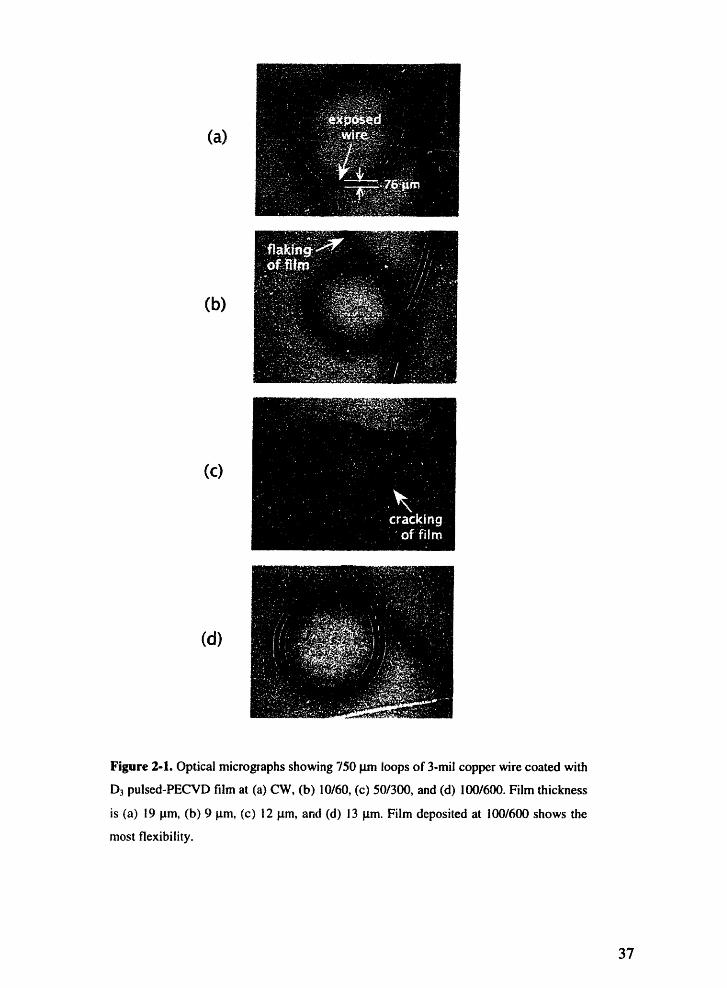
deposited at the same duty cycle f 14% but with different on- and off-times. Coatings
deposited under continuous-wave excitation (Figure 2-1a) showed considerable cracking
and flaking under tension, while coatings deposited at a lower luty cycle of 14% showed
improved flexibility (Figure 2-lb through 2-1d). In particular, cracking and flaking was
reduced as the on-time and off-time were increased, as illustrated by the good flexibility
of the 100/600 film. Indeed, of all the coatings tested, only the coating deposited at
100/600 did not crack, despite being more than 50% thicker than the 50/600 film (a duty
cycle of 8%). This suggested that, though thickness may be important in determining
flexibility, the effect of pulsing plasma excitation is more significant. Coatings on wires
were conformal, as illustrated by a cross-sectional ESEM of film deposited on a
University of Michigan (UM) probe (Figure 2-2).
36
(a)
(b)
(C)
(d)
Figure 2-1. Optical micrographs showing 750 pm loops of 3-mil copper wire coated with
D3 pulsed-PECVD film at (a) CW, (b) 10/60, (c) 50/300, and (d) 100/600. Film thickness
is (a) 19 m, (b) 9 gm, (c) 12 m, and (d) 13 m. Film deposited at 100/600 shows the
most flexibility.
37

Figure 2-2. Coating on a University of Michigan probe deposited at 50/300,
showing conformity of coating. Film is 20 gm at the thickest point.
Soak Testing. Multiple samples of pulsed-PECVD films were placed under
saline soak at 80°C and the leakage current was monitored over time. Results to date
(Table 2-2) indicate that many of the films still survive after nearly a year under soak.
Films are robust and appear to adhere well to silicon surfaces. In particular, the 100/600
film that showed good flexibility has proved resistant to prolonged exposure to warm
saline solution. Bulk resistivities for these films are lower than observed for high-quality
silicones (typically 1016 Q-cm), but are acceptable for our applications. Failure mode was
determined by examination of failed films under an optical microscope. The failure mode
observed for the pulsed-PECVD samples appeared to be defect inclusion, where a
pinhole or particulate caused a loss in insulating characteristics, while the CW films
failed primarily through cracking.
38

Table 2-2. Results of saline soak testing of pulsed-PECVD films
deposited under a variety of pulse conditions.
duty cycle plasma no. of years under survival rate average(%) excitation samples soak (%) resistivitya
tested (2-cm)100 CW 8 1.23 88 4.5-1012
CW 4 0.90 100 3.3-101333 100/200 4 0.90 75 2.3-10'1320 100/400 8 1.23 75 1.6-1013
100/400 8 0.90 100 4.7 101314 10/60 8 0.90 75 5.8-1013
50/300 4 0.73 75 2.9 1013100/600 4 0.90 100 4.7-1013
9 10/100 8 1.23 88 4.6 10'3
10/100 4 0.90 10i 2.010'143 10/250 b 4 0.90 50 9.1 1012
average 84 4.6.10'
a Error in resistivity for each sample over time was snall, typically less than 5%.b
The 10/250 film was considerably thinner than other samples tested, which may account for its poor soak performance.
Film Structure. The FTIR spectrum of a 100/600 film is compared to that of the
bulk polymer polydimethylsiloxane (PDMS) in Figure 2-3. Major assignments have been
made in Table 2-3 based on :he literature.26 3 '
Cee
Z
aOtJW
CeUEu0'A
0MIn
4000 3500 3000 2500 2000 1500 1000 500
wavenumber (cm')
Figure 2-3. FTIR spectra of (a) pulsed-PECVD film deposited at 100/600, and (b) PDMS secondary
standard. Absorption spectra of pulsed-PECVD film has been normalized to standard thickness of 1,500 A.
39

Table 2-3. FTIR assignments from the literature.
wavenumber (cm') modea comment references
2964 - 2967 VA in sp 3 CH3 26,28.30
2933 VAcH in sp3 CH 2 26,30
2907 - 2909 vs in sp3 CH3 26,28.30
2878 VsCH in sp 3 CH 2 26.30
1463 A2 26,30
1413 6Ac 3 in SiMe,, 26,28.3031
1263 SC3 in SiMe, 26,28.29.31
1028 - 1120 V siosi 262830.3
895 Vsi-. PCH3 in SiMe 2 26.28.29.31
803 Vsi-C, PCH3 in SiMe2 26.28,29.31
845 - 850 Vsi-. PcH3 in SiMe 3 26.28.29.31
760 Vsi-c, PCH3 in SiMe3 26.28.2931
780 Vsi-c in SiMe, 26.29
a v, 6 and p denote stretching, bending and rocking modes respectively, a and s denote asymmetric and symmetric vibrations.
The spectrum for the pulsed-PECVD film bears some resemblance to that
obtained previously for PECVD films from organosilicon precursors. 26 Of particular note
is the strong doublet centered around 1090 cm-' , identified as the asymmetric stretching
mode (ASM) of a polymeric siloxane backbone. The ratio of the two peaks of this
doublet has been correlated with the length of chains or size of rings in the
polymethylsiloxane network.2 6' 32 In particular, for a series of linear and cyclic
polymethylsiloxanes of increasing chain length or ring size, a doublet was observed in
FTIR spectra only when chain lengths exceeded two siloxane units and ring size
exceeded eight siloxane units. Hence, the films produced by pulsed-PECVD show some
polymeric character. 32 Strong absorptions are observed near 800 cm-' and 850 cm-' and
have been assigned to di- and tri-methyl substituted silicon atoms. The strong band at
1,263 cm-' represents the bending mode for a silicon-bonded methyl group. Absorptions
correlated to CHx groups are observed at higher wavenumbers. For this sample, only sp 3-
hybridized carbon bonding is observed. Comparison of the FTIR spectra reveals that
plasma excitation timing can strongly influence film structure. Films deposited at duty
cycles of 100% (CW), 14% (100/600) and 2.4% (10/400) show the most variation both in
the silicon-correlated and carbon-correlated regions (Figures 2-4 and 2-5).
40

-_
8Li.0
4e
.0
'e
1400 1200 1000 800 600
wavenumber (cm - ')
Figure 2-4. FTIR spectral region from 600 cm' to 1,500 cm -' for CW, 100/600 and 10/400 films.
Respective duty cycles are 100%, 14% and 2.4%.
._
-0
a
U.0
en.0ra
3050 3000 2950 2900 2850 2800wavenumber (cm' ')
Figure 2-5. FTIR spectral region from 3,050 cm' to 2,800 cm' for CW, 100/600 and 10/400 films,
showing CHx correlated absorptions.
The spectra of films deposited at duty cycles ranging from 33% to 8% bore a
close resemblance to that of the 100/600 film. Of particular note is the 100/200 film,
which was deposited at the same equivalent power as the CW film (100 W), where
equivalent power is obtained by multiplying duty cycle by peak power. The FTIR
spectrum of the 100/200 film (not shown) resembles that of the 100/600 film rather than
41

that of the CW film. Thus, the difference in structure between CW and pulsed-PECVD
films is attributed to the effect of pulsing rather than that of equivalent power.
In the region from 600 cm - ' to 1500 cm- ' (Figure 2-4), the spectrum of the CW
film shows a shift to higher wavenumbers for the ASM and an increase in the intensity of
the peak at 900 cm -'. The peak at 900 cm-' is in the region usually assigned to the
stretching and bending modes for SiMe 2. Typically, this peak has been reported at lower
wavenumbers than observed here, as for instance in the work of Rau et a126, who
observed the peak at 885 cm-'. It is odd that an increase in intensity for this peak is
coupled with a reduction in intensity for the peak also associated with SiMe2 at 803 cm -'
for the CW film, although this may be due to steric effects. Since no literature was found
to suggest any other assignment, the SiMe 2 assignment is thus made tentatively. A band
of low intensity at 780 cm -' is more pronounced for the CW film and corresponds to
SiMel stretching. This suggests the presence of silicon atoms which may be involved in
crosslinking and/or branching. We have identified two categories of crosslinks and/or
branches: Type I, which consists of siloxane sidechains originating from nodes where
silicon is attached to more than two oxygen atoms; and Type II, which consists of carbon
sidechains originating from methylene-substituted multi-oxygen nodes. These categories
are illustrated structurally in Figure 2-6. Here, M, D, T and Q represent silicon atoms
with increasing numbers of oxygen substituents, and DCH 2, D(CH 2)2 and TCH2 represent
D and T groups with methylene substituents. Note that Figure 2-6 is not intended to be a
rigorous summary of the silicon bonding environments present in our PECVD films.
Indeed, hydrogen substituted versions of M through Q (typically referred to as MH, DH,
etc.) have been observed in 29Si solid-state NMR analysis of these films, and other
structural variations are possible.
42

Non- TYPE TYPEBranched i 11
CH3 O CH,
CH3 CH3 (IH2)
I ?, I
CH3 0O' (CH),
(CH2),
| TCHJ |
note : x = or 1
Figure 2-6. Possible crosslinking and/or branching nodes present in PECVD films. Non-
branching M and D groups are shown for reference. Nodes of Type I involve only
oxygen, while nodes of Type II involve both oxygen atoms and methylene groups.
Both CW and pulsed-PECVD films show a lower methyl content than PDMS
(compare Figures 2-3a and 2-3b). This confirms, as does the hardness of the films, that
crosslinking groups are present in the films. Indeed, T and Q groups have been clearly
observed in PECVD organosilicon films by other workers3 3 and in our own laboratory
using solid-state 29Si NMR spectroscopy. Crosslinks of Type I are thus present in both
CW and pulsed-PECVD films. In the CW film, absorptions associated with methylene
groups are observed at 2,933 cm 'l and 2,878 cm-' (Figure 2-5). This is consistent with an
absorption of low intensity at 1,463 cm-', also attributed to the presence of the methylene
group, as well as the lower relative intensity of the methyl band at 1 263 cm-' for the CW
film. Additional analyses on several of these films, including XPS and solid-state 29Si
NMR, have indicated that pulsed-PECVD films are more oxidized than their CW
counterparts and contain more T and Q groups. For instance, a 10/60 film analyzed using29Si SSNMR showed 0.6% more T groups and 3.2% more Q groups than a CW film.
43

Considering the enhanced flexibility observed in pulsed-PECVD films, this suggests that
methylene is present in CW films primarily in the form of carbon crosslinks rather than
as carbon sidechains. These carbon crosslinks are of Type II and originate from DCH 2,
D(CH2)2 and TCH2 nodes. Whether methylene is bonded as Si-CH 2-Si or Si-(CH 2)2-Si is
uncertain. Previous workers have argued that even a small absorption at 1,360 cm-' is
evidence of the former, but no assignment has been made in this work.26 The lack of
methylene crosslinking groups in pulsed-PECVD films suggests that there may be more
pathways available for incorporation of oxygen during pulsed excitation than during CW
excitation. With just a single type of crosslinking group, reasonable mechanical
flexibility can still be retained.
The intensities of both the SiMe 3 absorptions (at 845 cm-') and the SiMe 2
absorptions (at 803 cm- l) are lower in the CW film than in the pulsed-PECVD films.
However, the ratio of the intensities of SiMe 3 to SiMe 2 is higher for the CW film than for
the pulsed-PECVD films. This suggests that there are more terminal groups per
polymeric siloxane (or D) unit in the CW film. Two main differences in structure are
postulated to account for this. First, polymeric segments in the CW film may be shorter
on average than those in the pulsed-PECVD film. These segments could be main chains
or sidechain branches attached to a main chain. Second, since ring structures preclude the
possibility of SiMe 3 groups, the CW film may have less ring structure overall than the
pulsed-PECVD films. A more highly branched structure in CW films would also be
consistent with an increase in the ratio of endgroups to backbone groups. The poor
flexibility of CW coatings, however, suggests that these films are highly networked,
rather than highly branched.
Mechanisms of plasma polymerization have been considered by various authors,
notably Wr6bel et all, who provide a good overview of plasma-polymerized
organosilicon materials. They argue that the dominant mode of precursor fragmentation is
methyl abstraction, and that the active species in polymerization are primarily ionic in
nature. In particular, an ionic mechanism for the ring expansion of D3 during
oligomerization is proposed. 34 35
The thermal decomposition of cyclic polydimethylsiloxanes has also been
investigated. 36 '3 8 Davidson and Thompson, in particular, considered the pyrolysis of D4
44

and estimated kinetic parameters for some proposed decomposition pathways. Based on
their work, we have identified possible reaction pathways for the production of
polymerization precursors from the decomposition of D3, as shown in Scheme 1.
1. D3 - D2 + Di decomposition
2. D3 -- Me. + Me 5 03Si 3- methyl abstraction
3. D3 - I-D3 ring opening
Scheme 2-1. Reaction pathways for the production of polymerization precursors from D3 .
Dl in reaction 3 is the intermediate dimethylsilanone, Me2Si=O. It is a potential
film growth species that could lead to structures analogous to linear PDMS chains. The
abstraction of a methyl group from D 3, as represented by reaction 2, may take place via
electron impact, and may result in a ionic silicon species rather than the radical species
proposed for thermal decomposition. The presence of ionic silicon species in plasmas has
been predicted and confirmed by other workers.39 4 2 Mass spectrometry has been used to
directly sample the reaction species from an RF plasma consisting of a mixture of
vinyltrimethylsilane (VTMS) and argon. The distribution of ionic and neutral products
indicated that successive dissociation and ionization of VTMS by low energy electron
impact was the dominant mode of energy transfer at high pressures (> 0.5 Torr).42 '4 3
These results suggest that ion and radical chemistries may both be important in
organosilicon plasmas.1' 34
In their pyrolysis experiments, Davidson and Thompson observed reaction 2 to be
much faster than reaction 1. The Si-O bond in cyclosiloxanes has been found to be
exclusively stable to homolytic cleavage, and the ring-opening of D3 to form the biradical
*Me2Si(OSiMe 2)2 0 by reaction 3 unlikely.44 The radical or ion produced by reaction 2
may thus be of some importance in plasma polymerization. Its existence suggests that
film growth may involve the incorporation of oligomeric cyclic groups in addition to
linear chains. It is interesting to speculate that the right-hand peak of the ASM near 1,020
cm-' may be due to the presence of bound six-membered D 3-like rings within the film. In
a series of IR spectra of cyclic polymethylsiloxanes from D 3 up to D8, Wright et al.
45

observed that the ASM consisted of a single peak for ring structures smaller than Ds. This
peak was offset at 1,020 cm-' for D3 due to higher ring strain. By this reasoning, the FTIR
data indicate that films of lower duty cycle incorporate a higher proportion of six-
membered D3-like rings into their structure. Specifically, the FTIR spectrum for the
10/400 film in Figure 2-1 bears a closer resemblance to that of the precursor than the
100/600 film. The FTIR spectrum for high molecular-weight PDMS (Figure 2-3b),
however, does show an ASM doublet with a peak close to 1,020 cm-', making it difficult
to differentiate between the presence of long chains and bound D3 rings.3 2 To form a
network of rings, at least two methyl abstraction events are required per precursor
molecule. In previous work, we have investigated films deposited from D 4 using
pyrolytic CVD. From elemental analysis, we observed that 1.9 methyl groups were lost
per D4 molecule, offering strong evidence for the incorporation of precursor-like rings
into the film structure.45 For PECVD films, the destructive nature of the plasma means
that both linear and ring structures are likely to coexist even for films deposited at low
duty-cycle films. It is not yet clear whether the characterization techniques available to us
are capable of separating these different structural forms.
2.5 Conclusions
Pulsed-PECVD of D3 offers a means of producing thin conformal, and insulating
coatings at reasonable rates with adequate resistance to prolonged immersion in warm
saline solution. Deposition was demonstrated on nonplanar substrates suitable for
implantation, such as copper wires and neural probes. Wire coatings produced by pulsed-
PECVD show more flexibility than CW coatings.
Both CW and pulsed-PECVD show evidence of crosslinking via T and Q groups.
The carbon in pulsed-PECVD films is predominately bonded as CH 3, indicating retention
of methyl groups from the D3 precursor. By contrast, both CH 3 and CH 2 groups are
observed in CW films. These methylene units, when bonded to D, T, or Q groups,
constitute a crosslinking node we have designated as Type II. Type II crosslinks are
characterized by carbon bridges of the form Si-(CI 2)n-Si (n I). The presence of
crosslinking groups of both Type I and Type II in CW films leads to a highly networked
structure, and results in brittle coatings on thin wires. Methylene was not detectable in the
46

pulsed-PECVD films, suggesting that formation of Type II crosslinks requires a longer
plasma decomposition period.
Endgroups and sidechain terminations of the form SiMe 3 are prevalent in the CW
film, indicating short chains and/or highly branched structures. In the pulsed-PECVD
film, SiMe 2 is the predominate mode of methyl incorporation, consistent with enhanced
retention of the precursor structure under conditions where plasma fragmentation
processes are limited. Films with primarily SiMe 2 bonding must be either long linear
siloxane chains and/or networks of interconnected ring structures. Polymerization of
dimethylsilanone is one mechanism which could result in the growth of long linear
chains. Six-membered D3 rings and larger may be present in films produced by pulsed-
PECVD, where neutral chemistry is more likely to compete with ionic chemistry and
precursor fragmentation is expected to be less. This could explain the higher proportion
of terminal methyl groups observed in FTIR of CW films, since these groups do not
appear in siloxane ring structures.
Acknowledgements. We gratefully acknowledge the support of the NIH under
contract NO I-NS-9-2323 and the NSF/SRC Engineering Research Center for
Environmentally Benign Semiconductor Manufacturing in funding this work. In addition,
this work made use of MRSEC Shared Facilities supported by the NSF under award
DMR-9400334.
2.6 References
i. A. M. Wr6bel and M. R. Wertheimer, in Plasma Deposition, Treatment, and Etching of Polymers,
R. d'Agostino, Editor, p. 163, Academic Press, San Diego, CA (1990).
2. F. F. Shi, Surf. Coat. Tech., 82, 1 (1996).
3. Z. Ogumi, Y. Uchimoto, and Z. Takehara, J. Electrochem. Soc., 136, 625 (1989).
4. M. Kusabiraki, J. Appl. Polym. Sci., Appl. Polym. Symp., 46, 473 (1990).
5. P. K. Tien, G. Smolinsky, and R. J. Martin, Appl. Opt., 11, 637 (1972).
6. A. S. Chawla, A:;if: Organs, 3, 92 (1979).
7. A. S. Chawla, Biomaterials, 2, 83 (1981).
47

8. Y. Ishikawa, S. Sasakawa, M. Takase, Y. Iriyama, and Y. Osada, Makromol. Chem, Rapid
Commun., 6, 495 (1985).
9. N. Hasirci, J. Appl. Polym. Sci., 34, 2457 (1987).
10. J. G. Cannon, R. O. Dillon, R. F. Bunshah, P. H. Crandall, and A. M. Dymond, J. Biomed. Mater.
Res., 14, 279 (1980).
11. H. Matsuyama, A. Kariya, and M. Teramoto, J. Appl. Polym. Sci., 51, b89 (1994).
12. M. F. Nichols, Crit. Rev. Biomed. Eng., 22, 39 (1994).
13. M. F. Nichols, Biomed. Sci. Instrum., 29, 77 (1993).
14. H. Yasuda and T. Hsu, J. Polym. Sci., Polym. Chem. Ed., 15, 81 (1977).
15. A. Bouchoule and P. Ranson, J. Vac. Sci. Technol. A, 9, 317 (1991).
16. S. G. Hansen, G. Luckman, and S. D. Colson, Appl. Phys. Lett., 53, 1588 (1988).
17. A. Kono; M. Haverlag, G. M. W. Kroesen, and F. J. de Hoog, J. Appl. Phys., 70, 2939 (1991).
18. C. B. Labelle, S. J. Limb, and K. K. Gleason, J. Appl. Phys., 82, 1784 (1997).
19. S. J. Limb, K. K. S. Lau, D. J. Edell, E. F. Gleason, and K. K. Gleason, Plasmas Polym., 4, 21
(1999).
20. K. K. S. Lau and K. K. Gleason, J. Fluorine Chem., 104, 119 (2000).
21. C. R. Savage, R. B. Timmons, and J. W. Lin, in Adv. Chem. Ser., 236, p. 745, American Chemical
Society, Washington, DC (1993).
22. V. Panchalingam, B. Poon, H.-H. Huo, C. R. Savage, R. B. Timmons, and R. C. Eberhart, J.
Biomater. Sci. Polym. Edn., 5, 131 (1993).
23. N. M. Mackie, N. F. Dalleska, D. G. Castner, and E. R. Fisher, Chem. Mater., 9, 349 (1997).
24. V. Panchalingam, X. Chen, C. R. Savage, R. B. Timmons, and R. C. Eberhart, J. Appl. Polym.
Sci., Appl. Polym. Symp., 54, 123 (1994).
25. M. J. Vasile and G. Smolinsky, J. Electrochem. Soc., 119, 451 (1972).
26. C. Rau and W. Kulisch, Thin Solid Films, 249, 28 (1994).
27. D. R. Anderson, in Analysis of Silicones, A. L. Smith, Editor, 41, p. 407, Wiley, New York
(1974).
28. H. Kriegsmann, in Advances in Molecular Spectroscopy; Proceedings, A. Mangini, Editor, 3, p.
1000, Pergamon Press, New York (1962).
29. L. J. Bellamy, The Infra-red Spectra of Complex Molecules, 2nd ed., p. 334, John Wiley & Sons,
Inc., New York, (1958).
30. K. M. McNamara, B. E. Williams, K. K. Gleason, and B. E. Scruggs, J. Appl. Phys., 76, 2466
(1994).
31. R. E. Richards and H. W. Thompson, J. Chem. Soc., 124 (1949).
32. N. Wright and M. J. Hunter, J. Am. Chem. Soc., 69, 803 (1947).
33. 1. Tajima and M. Yamamoto, J. Polym. Sci., A, Polym. Chem., 25, 1737 (1987).
34. A. M. Wr6bel, M. Kryszewski, and M. Gazicki, J. Macromol. Sci. - Chem., A20, 583 (1983).
48

35. M. Kryszewski, A. M. Wr6bel, and J. Tyczkowski, Am. Chem. Soc., Plasma Polym. , 108, 220
(1979).
36. I. M. T. Davidson and J. F. Thompson, Chem. Comm., 251 (1971).
37. I. M. T. Davidson and J. F. Thompson, J. Chem. Soc., Faraday Trans. 1, 71, 2260 (1975).
38. L. E. Gusel'nikov, N. S. Nametkin, T. K. Islamov, A. A. Sobtsov, and V. M. Vdovin, Izvest. Akad.
Nauk SSSR, Ser. Khimi., 20, 84 (1971).
39. A. K. Hays, in Plasma Processing, J. Dieleman, R. G. Frieser, and G. S. Mathad, Editors, 82-6, p.
75, The Electrochemical Society (1981).
40. A. K. Hays, Thin Solid Films, 84, 401 (1981).
41. G. Smolinsky and M. J. Vasile, Int. J. Mass Spectrom. Ion Phys., 12, 147 (1973).
42. M. J. Vasile and G. Smolinsky, Int. J. Mass Spectrom. Ion Phys., 13, 381 (1974).
43. M. J. Vasile and G. Smolinsky, Int. J. Mass Spectrom. Ion Phys., 12, 133 (1973).
44. M. G. Voronkov, J. Organomet. Chem., 557, 143 (1998).
45. M. C. Kwan and K. K. Gleason, CVD, 3, 299 (1997).
49

PTER 3) of Organosiliconms from D 3 and D 4
s, TB Casserly, KK Gleason, submitted to J. Electrochem. Soc.
50

3.1 Abstract
A non-plasma technique, hot-filament chemical vapor deposition (HFCVD), is an
alternative method to produce organosilicon films of novel structure. Films are deposited
onto room temperature substrates from the precursors hexamethylcyclotrisiloxane (D3)
and octamethylcyclotetrasiloxane (D4) at high rates (>1 micron/min). Filament
temperature can be used to control film structure, and the limited reaction pathways
available via thermal decomposition make it possible to elucidate the chemistry of the
growth process. During film growth, there appears to be competition between reaction
pathways for the incorporation of cyclic and linear siloxane structures. For both D 3 and
D4 HFCVD films, Infrared, Raman, and Nuclear Magnetic Resonance spectroscopies
indicate the incorporation of ring structures consisting of three siloxane units (oR3). The
concentration of these structures increases as filament temperature is raised, and is
especially pronounced for films from D3. In comparison, films from D4 show a greater
degree of incorporation of linear, unstrained structures over the range of filament
temperatures studied. In contrast to PECVD organosilicon films, crosslinking in HFCVD
films occurs predominantly via silicon-silicon bonding and not from ternary or
quaternary siloxane bonds.
51
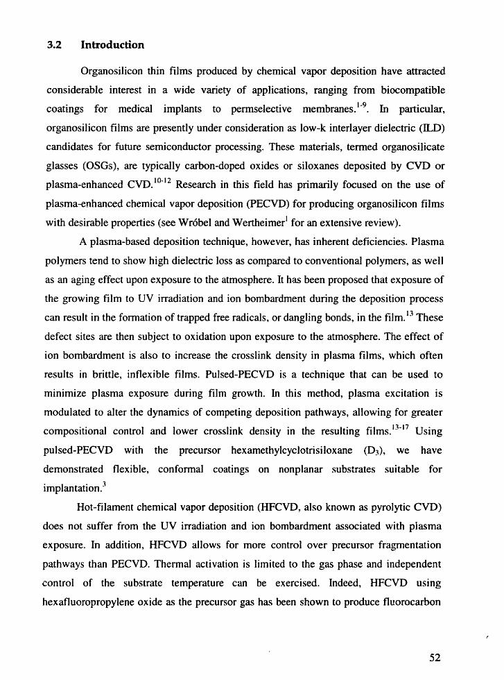
3.2 Introduction
Organosilicon thin films produced by chemical vapor deposition have attracted
considerable interest in a wide variety of applications, ranging from biocompatible
coatings for medical implants to permselective membranes. 9 . In particular,
organosilicon films are presently under consideration as low-k interlayer dielectric (ILD)
candidates for future semiconductor processing. These materials, termed organosilicate
glasses (OSGs), are typically carbon-doped oxides or siloxanes deposited by CVD or
plasma-enhanced CVD.'l 0- 2 Research in this field has primarily focused on the use of
plasma-enhanced chemical vapor deposition (PECVD) for producing organosilicon films
with desirable properties (see Wr6bel and Wertheimer' for an extensive review).
A plasma-based deposition technique, however, has inherent deficiencies. Plasma
polymers tend to show high dielectric loss as compared to conventional polymers, as well
as an aging effect upon exposure to the atmosphere. It has been proposed that exposure of
the growing film to UV irradiation and ion bombardment during the deposition process
can result in the formation of trapped free radicals, or dangling bonds, in the film.' 3 These
defect sites are then subject to oxidation upon exposure to the atmosphere. The effect of
ion bombardment is also to increase the crosslink density in plasma films, which often
results in brittle, inflexible films. Pulsed-PECVD is a technique that can be used to
minimize plasma exposure during film growth. In this method, plasma excitation is
modulated to alter the dynamics of competing deposition pathways, allowing for greater
compositional control and lower crosslink density in the resulting films."3 ' 7 Using
pulsed-PECVD with the precursor hexamethylcyclotrisiloxane (D 3), we have
demonstrated flexible, conformal coatings on nonplanar substrates suitable for
implantation.3
Hot-filament chemical vapor deposition (HFCVD, also known as pyrolytic CVD)
does not suffer from the UV irradiation and ion bombardment associated with plasma
exposure. In addition, HFCVD allows for more control over precursor fragmentation
pathways than PECVD. Thermal activation is limited to the gas phase and independent
control of the substrate temperature can be exercised. Indeed, HFCVD using
hexafluoropropylene oxide as the precursor gas has been shown to produce fluorocarbon
52
films with low dangling bond density and having a chemical structure which is
spectroscopically similar to polytetrafluoroethylene (PTFE). 7.-8
In this study, we consider the structure of films produced by HFCVD using the
precursors hexamethylc-clotrisiloxane, [(CH3)2SiO]3, and octamethylcyclotetrasiloxane,
[(CH) 2Si0]4 , commonly known as D3 and D4. Previously, we demonstrated that
polymeric thin films could be deposited from D 4 by HFCVD at rates of up to 25,000
A-min -1 depending on filament temperature.' 9 In this work, we show that filament
temperature (Tf) has a strong influence on composition for both D 3 and D4 HFCVD films,
and postulate a structure for these novel films.
3.3 Experimental
Films were deposited on silicon wafer substrates in a custom built vacuum
chamber. Thermal excitation was accomplished by resistively heating tantalum wire
(diameter 0.5 mm) strung on a filament holder. Springs on the holder maintained wire
tension to compensate for thermal expansion and prevent drooping. The filament wire
was mounted in a parallel array designed to minimize thermal gradients between
individual wires and offer uniform heating over an area the size of a wafer. The filament
holder straddled a cooled stage on which a silicon wafer substrate was placed. A filament
to substrate standoff of 1.3 cm was used. Pure precursor was vaporized in a heated vessel
and delivered through a needle valve to maintain flow rates of approximately 14 sccm for
D 3 and 11 sccm for D4. Pressure in the reactor was maintained at 300 mTorr by a
butterfly valve. No diluent gas was used.
Filament temperature was measured using an 2.2 m infrared pyrometer. For
oxidized tantalum, a spectral emissivity of 0.20 was estimated from direct contact
thermocouple measurements. Given the difficulties of dilect measurement at high
temperatures, reported temperatures are probably accurate to 50°C. However,
temperatures were consistent from run to run and there was little variation in power
requirements for heating the wire. Substrate temperature was maintained below 60°C by
backside water cooling. Films were deposited on 4-inch silicon wafers at filament
temperatures ranging from 800°C to 1200°C. Deposition rates were monitored in situ
53

using interferometry and checked using profilometry at the center of each wafer after
deposition.
For film characterization, infrared spectroscopy was performed using a Nicolet
Magna 860 FTIR spectrometer operating in transmission mode. All spectra were
normalized to a standard thickness of 1500 A and baseline corrected for purposes of
comparison. Resonant Raman spectra were obtained using a Kaiser Optical Systems
Hololab 5000R Modular Research Micro-Raman Spectrograph, with 785 nm laser line
excitation and 15 mW power at the sampling stage under 50x magnification. High
resolution solid-state NMR spectra were acquired on a homebuilt NMR spectrometer20
equipped with a 6.338 T Oxford superconducting magnet and a 3.2 mm Chemagnetics
probe with spinning capabilities up to 25 kHz. Magic angle spinning (MAS) and cross-
polarization (CP) from the proton spin bath were used to resolve isotropic chemical shifts
and reduce acquisition time. Approximately 10 mg of film was scraped off the wafer and
packed into a zirconia rotor, which was spun at 7 kHz. 14,512 acquisitions were
performed for signal averaging. A 'H-29Si CP time of 5 ms was chosen to maximize the
overall signal intensity. Experiments confirmed that the contact time between the silicon
and proton spin baths was sufficient to provide uniform 29Si polarization. Indeed, a
direct comparison of NMR spectra acquired with direct- and cross-polarization confirmed
that CP spectra were quantitative. All NMR spectra were referenced to tetramethylsilane
(TMS) and are plotted in ppm. X-Ray Photoelectron Spectroscopy (XPS) was
performed on a Kratos AXIS ULTRA spectrometer using a monochromatized aluminum
K-a source. Atomic force microscopy (AFM) was performed on a Digital Instruments
Dimension 3000. Images were taken under tapping mode with a standard etched silicon
tip.
3.4 Results and Discussion
Deposition Rate. As shown in Figure 3-1, the deposition rate appears to follow
an Arrhenius-type relationship as a function of filament temperature. The highest
deposition rate observed was 15,740 A/min, for D4 at a filament temperature of 1050°C.
No film deposition was detected at filament temperatures below 800°C with either
precursor. At the higher filament temperatures, run times were limited to 1.5 minutes to
54

produce thin films appropriate for subsequent characterization. These temperatures are
consistent with other studies of the vacuum pyrolysis of D4.21 Regression of the data in
Figure 3-1 yielded apparent activation energies of 218+35 kJ/mol for D 3, and 301+102
kJ/mol for D4 (at a 90% confidence level).
T, (C)-S 1200 1100 1000 900 800
lu-
g' 104
E
-Z
103
,
Q. 102
1010.65 0.70 0.75 0.80 0.85 0.90 0.95
103T, (104 K')
Figure 3-1. Arrhenius plot of D3 and D4 films produced by HFCVD.
Straight lines were fitted by regression.
Fourier-Transform Infra-Red (FTIR) Spectroscopy. A comparison of the
FTIR spectra of D3 films deposited using HFCVD and continuous-wave excitation
PECVD is shown in Figures 3-2a and 3-2b. The spectra for the CW PECVD film (Figure
3-2a) was taken from previous work by our group.3 Assignments have been made from
the literature and are shown in Table 3-1. Comparison of these spectra indicated that the
HFCVD film differs structurally from the PECVD film. Only sp3-carbon bonding is
observed in the HFCVD film, and no crosslinking of Type II, i.e. via carbon-crosslinks, is
evident.3 Carbon is thus preserved primarily as methyl, giving rise to the distinct pair of
symmetric and asymmetric CH stretches at 2907 and 2964 cm'l . The asymmetric
stretching mode (ASM) of the siloxane group (SiOSi) shows two distinct peaks for the
HFCVD film, a characteristic observed in the IR signatures of polydimethylsiloxanes
with chain lengths of more than two siloxane units or ring sizes of larger than eight
units. 22'23 Below 1000 cm-', absorption bands associated with SiMe 2 rocking and
stretching are observed at 878 and 805 cm-', and those associated with SiMe 3 rocking
55
,,,, , , ,- , i , , , I , , , i , , ,
--- D4
--- D3
O\ xX \~~~~
\~~~~m

near 840 cm l'. Qualitatively, the PEVD films appears to have a higher SiMe 3/SiMe 2 ratio,
suggesting that the HFCVD films is less branched than its PECVD analog.3
D
'U
-o0.0
4000 3500 3000 2500 2000 1500 1000 500
wavenumber (cm-')
Figure 3-2. FTIR spectra of a. D3 PECVD film deposited under continuous-wave excitation,
and b. D3 HFCVD film deposited at I 000°C.
Table 3-1. FTIR assignments from the literature.
wavenumber (cm -') modea comment ref.
2963 - 2965 VACH in sp CH3 24.-272935 VACH in sp CH2 26.27
2907 vSCH in sp 3 CH3 24-272878 vsc{H in sp 3 CH 2 26.27
1463 5ACH2 26.27
1412 AAC,3 in SiMe, 23-27
1262 /SCH3 in SiMeC 23-25.27.28
1020- 1075 V siosi 23-27
878 PSCH3 in SiMe2 23.24.27.28
804 - 806 V SlC, PA CH3 in SiMe 2 232.27.28
839 -845 pACH3 in SiMe3 23.,4.27.28
v, and p denote stretching, bending and rocking modes respectively, a and s denote asymmetric and symmetnc vibrations.
FTIR spectra of films deposited at filament temperatures of 860°C, 1000°C, and
1200°C using D3, and 800°C, 900°C, and 1000°C using D4, are also shown (Figures 3-3
and 3-4, respectively). The region around the ASM has been expanded for detail. Strong
absorptions associated with SiMe2 (805 cm-l), methyl in SiMex (1412 cml), and the
ASM (1020-1075 cm ') are apparent. The peak at about 880 cm"l observed in the low
56

filament temperature D4 film is usually associated with the symmetric CH3 rocking mode
in SiMe2. The disappearance of this band at higher filament temperatures may be due to
the conformational constraints present in a more highly networked structure. Similar
effects in this infrared region have been observed in temperature-dependent spectroscopy
studies of other organosilicon compounds. 29' 30
'U
v-,C.0
voUell
wavenumber (cm- ')
Figure 3-3. FTIR spectra of D3 HFCVD films deposited at filament
temperatures of a. 860°C, b. 1 000°C, and c. I 100°C.
57

C
-0c'
VC0.e't~oe
wavenumber (cm- ' )
Figure 34. FTIR spectra of D4 HFCVD films deposited at filament
temperatures of a. 800°C, b. 900C , and c. 1 000C.
Conventionally2 3 27 2 8, the peak around 845 cm- ~ is assigned to an asymmetric
CH 3-rocking mode in SiMe 3, with an accompanying symmetric CH 3-rocking mode at 760
cml1. The SiMe 3 group is a chain or branch termination group that is associated with an
M group in siloxanes. 3. The relative intensities of the SiMe 2 and SiMe 3 bands depends on
the length of chains in open-chain regions of the film structure, and the strength of the
SiMe 3 peak is an indication that chains are either short or highly branched. 222 5 The
SiMe 3/SiMe 2 ratio also increased only slightly as filament temperature was increased,
suggesting that the chain length and branching was similar for both sets of films. Other
data obtained for these films, particularly from NMR analysis, show only small quantities
of M groups in the films, with the highest concentrations appearing in low filament-
temperature D3 and high filament-temperature D4 films. This implies that short chain
segments or branches of similar length are present in low concentrations in almost all the
films produced.
Significant changes in the relative intensities of the peaks of the ASM band are
observed for both D 3 and D 4 films. The D3 film shows a doublet for all three filament
58

temperatures, with the shoulder on the doublet switching from the low- to high-
wavenumber side at higher filament temperatures (compare Figures 3-3a and 3-3c). By
contrast, the D4 film deposited at a filament temperature of 800°C showed only a singlet,
and the IR spectra resembled that of the precursor D4.22' 23 Unlike D4, however, which is a
liquid at room temperature, the film was solid and contiguous and came off the wafer in
flakes when scraped with a razor. Little SiMe 3 was detected in this film. The D4 film
deposited at higher filament temperature showed behavior similar to that of the D3 film.
As filament temperature was increased, the low-wavenumber peak of the ASM doublet
increased in intensity, exceeding that of the high-wavenumber peak above 1050°C
(spectra not shown), as in the case of the D3 film.
The ASM doublet of the film deposited from D 3 at a filament temperature of
I 100°C (Figure 3-3c) resembles that observed in FTIR analyses of other organosilicon
PECVD films. 3'27'31 Typically for these films, the low-wavenumber peak was more
intense than the high-wavenumber peak. This ASM signature is also observed in spin-on
methyl silsesquioxane (MSQ) films.3? For bulk polydimethylsiloxane (PDMS), the
intensities of these peaks are approximately equal at room temperature.33 To our
knowledge, no IR spectra with an ASM doublet similar to that observed in Figures 3-3a,
3-3b and 3-4c have been reported for organosilicon films deposited by CVD from
comparable precursors. The configuration of the ASM doublet is likely to be
conformational in origin. For PDMS, the splitting of the doublet has been attributed to
coupling between adjacent chain segments. 25 In other work using Raman spectroscopy,
the splitting of the symmetric SiOSi stretching mode has been correlated to the crystalline
state of PDMS.34
The intensity ratio of the two peaks of the ASM doublet has been correlated with
the length of chains or size of rings in the polymethylsiloxane network. 22' 23 27 In
particular, for a series of linear and cyclic polymethylsiloxanes of increasing chain length
or ring size, a doublet was observed in FTIR spectra only when chain lengths exceeded
two siloxane units and ring size exceeded five siloxane units. The ASM singlet for D3
was offset at 1,020 cm' compared to larger ring structure. The peak at 1,020 cm-' may
thus be associated with an increasing proportion of six-membered D 3-like rings in the
film structure. This is in the same region as the low-wavenumber peak of the ASM
59

doublet in PDMS, however, making it difficult to differentiate between the presence of
chains and bound D3 rings using IR analysis. 25
Raman Spectroscopy. Though some work has been done in characterizing pure
organosilicon compounds using Raman spectroscopy, little has been reported on the use
of Raman for characterizing more complex organosilicon materials, such as those
produced by CVD. Figure 3-5 compares the Raman spectra of the pure compounds D3,
D4, and PDMS with that of HFCVD films grown from D3 and D 4 using high filament
temperatures. Assignments in Table 3-2 have been made based on the literature. 24' 25 293 5
The symmetric siloxane stretching mode (SSM), which is weak in FTIR spectra, is strong
in the Raman spectra. The position of the symmetric siloxane Raman band is shifted to
higher wavenumbers for D3 due to ring strain, and bands associated with ring
deformation can be observed for both D3 and D4. 25 Raman spectroscopy is thus a
sensitive probe for observing ring structure. Indeed, Raman spectroscopy is capable of
identifying siloxane ring "defects" in SiO2 films produced by sol-gel36 '39 and CVD
processes.40 Raman spectra for these materials exhibit specific bands corresponding to
ring structures comprised of different numbers of silicon atoms. In particular, Raman
bands at 605 cm-' and 495 cm- ' in silica have been attributed to rings with three and four
siloxane units, termed R 3 and R4 respectively. 36 37 '39' 40
60

Raman shift (cm-')
Figure 3-5. Micro-Raman spectra of a. D3, b. D4, c. PDMS, d. D4 HFCVD film deposited at a filament
temperature of 1000°C, and e. D3 HFCVD film deposited at a filament temperature of 11000C.
Table 3-2. Raman assignments from the literature.
Raman shift (cm-') modea comment ref.
1410 &A 24.29,41
1260 - 1265 SCH3 24,29,41
795 VASiC In SiC2 24.29.35.41
707 - 712 vSsic In SiC2 24.29.35.41
690 P ACH3 29,35.41
581 VsSiOSi In D3 25,35.42
489 Vssiosi In PDMS 24,41
476 vssiosi and/or ring deformation In D4 35.41
450 Ring deformation In D3 and D4 3541
424 - 426 Possible Si-Si stretch 43
190 - 194 8Ssic in SiC 2 25,35
160 8ssic and twist In PDMS 25
145 s sic In D4 25
v, 6 and p denote stretching, bending and rocking modes respectively, a and s denote asymnuetric and symmetric vibrations.
61

As observed in Figure 3-5, the HFCVD films differ from the pure compounds the
Raman shift region from 400 cm' to 600 cm-'. Both HFCVD films show a peak in the
range 586 - 590 cm' l which is not observed in PDMS or other linear siloxane
compounds. 5 This is close to the band assigned to the siloxane symmetric stretching
mode (SSM) at 581 cm-' in pure D 3. During an experiment in which polarization of the
Raman beam was changed from the parallel to the perpendicular mode, the band in the
HFCVD film was also found to be polarized, which is consistent with results observed
for the SSM in D3. 25,35 This band may thus be evidence of a bound D 3-like ring structure
in the film. The 5 - 10 cm'l shift from the position of this band in D 3 may be
conformational in origin and a result of the strain of being locked into a semi-networked
structure. Such shifts are possible, and Table 3-3 shows Raman assignments for the SSM
mode in different chemical environments.
Table 3-3. Raman siloxane symmetric stretching mode (SSM) assignments
for various chemical environments.
structure Raman shift (cm-) comment ref.
R3, 600-608 In vitreous and/or CVD silica. 3640
oR3 586-590 In D3 and D4 HFCVD films.
D3 581-587 In D3. 25,35.42
D 489-497 In PDMS. 24.41
R4 490-495 In vitreous and/or CVD silica. 3640
oR4 and/or ID 485 In D13 and D4 HFCVD films.
D4 475-480 In D4 . 24.29.35,41
In the highly networked environment of vitreous and chemical vapor-deposited
silica, the characteristic vibrational mode of the three-membered planar ring of siloxane
units, R 3, has been observed at shifts as high as 608 cm'. 36 38'44 By contrast, the SSM
mode is typically observed from 581-587 cm-' for unconstrained D 3. The band around
590 cm-' for the HFCVD falls between these extremes, and is thus assigned to an oR3
group. The nomenclature is intended to represent an organically substituted ring
consisting of three siloxane units, which is bound into the film structure. By analogy,
there may also be rings consisting of four siloxane units bound into the film structure
62

(oR4). Table 3-3 shows that the peak at 485 cm-' observed primarily in D4 HFCVD films
falls between the SSM bands for D in PDMS, R4 in silica, and unperturbed D4. This
suggests that the band is associated with oR4 groups and/or unstrained siloxane units in
the film. The unstrained siloxane units may be present in linear structures or in ring
structures larger than four units, and are designated as ID. The predominance of these
groups in the D4 films, particularly at low filament temperature, suggest that they are
unique to the pyrolysis chemistry of D4 and may be the four siloxane-unit ring analog,
oR4.
The HFCVD films also show a peak at 425 cm-' not observed in any of the pure
compounds. No assignment could be found for this peak in the literature, but it is in the
region associated with a silicon-silicon stretching mode.43 The Si-Si stretch gives a strong
Raman band at 400 - 405 cm -' for hexamethyldisilane, and is highly sensitive to silicon
substituents. For polar substituents, shifts can be large. For example, the Si-Si stretching
mode for FMe2SiSiMe2F has been reported at 433 cm'l , a shift of 30 cm'l from the
unsubstituted disilane.4 5 Hence, this peak is tentatively assigned to an Si-Si bond in the
film structure.
Figure 3-6 and 3-7 show the effect of filament temperature as probed by Raman
spectroscopy. In Figure 3-6, films deposited from D3 show an increasing concentration
of oR 3 units and Si-Si bonds as filament temperature is increased, and the D3 film
deposited at 1100°C shows significant ring incorporation. FTIR spectra for these films
show a similar increase in intensity in the low-wavenumber peak of the ASM doublet
(see Figure 3-3). suggesting that this peak at 1020 cm-' is indeed associated with three
siloxane-unit ring structures. By contrast, films deposited from D4 show a strong peak at
485 cm-', assigned to the presence of oR4 and/or unstrained D units. A slight increase in
oR 3 incorporation is observed as Tf increases, but this band does not dominate as it does
in D 3 films. Hence, the D 3 and D4 films differ structurally at high filament temperatures,
despite the similarities in structures suggested by FTIR.
63

900 800 700 600 500 400 300 200 100
Raman shift (cm- ' )
Figure 3-6. Micro-Raman spectra of D3 HFCVD films deposited
at filament temperatures of 860°C, 1000°C, and 1100°C.
900 800 700 600 500 400 300 200 100
Raman shift (cm')
Figure 3-7. Micro-Raman spectra of D4 HFCVD films deposited
at filament temperatures of 800°C, 900C, and 1000°C.
64

Nuclear Magnetic Resonance (NMR) Spectroscopy. 29Si CP-MAS NMR
spectra were obtained for the D3 and D 4 HFCVD films and are shown in Figures 3-8 and
3-9. Typical chemical shifts reported in the literature for organosilicon CVD films are
included in Table 3 4.20,31,4649
I . , .. I .... I. i40 20
29Si ppm
' .... I....I.... I .... I ....
0 -20 -40 -60I .'' -I I - 'I
-80
Figure 3-8. 29Si Solid-State CP-MAS NMR spectra of D3 HFCVD film deposited
at filament temperatures of 860°C, 1000°C, and 1 100°C.
40 20 0 -20 -40 -60 -8029Si ppm
Figure 3-9. 29Si Solid-State CP-MAS NMR spectra of D4 HFCVD film deposited
at filament temperatures of 800°C, 900'C, and 1 000C.
65
1
...... .. ... ... ... .. . ... ... I . ..I . .. .. ... ... ... ... ..

Table 3-4. 29Si NMR structures and chemical shifts commonly observed
in organosilicon CVD films.
symbol structure chemical shift (ppm) ref.
M (SiO)Si (CH3)3 +6 31,49-51
MH (SiO)Si'(H)(CH3 )2 -6 474951
-10 in D3
D (SiO) 2Si'(CH3)2 -20 in D4 31.46,48,49,51
-22 in PDMS
DH (SiO)2 Si'(H)(CH 3) -34 to -37 46.47.49,51,52
T (SiO) 3Si'(CH3) -67 31.46,49.51
TH (SiO)3Sif(H) -84 20.47
Q (SiO)4 Si -105 to -110 31,46,48,49,51
As suggested by Table 3-4, films deposited by other CVD methods commonly
show a wide variety of bonding environments, including the presence of M, D, T, and Q
groups as well as their hydrogenated analogs. 31' 49'53 By contrast, only two primary peaks
were observed in these HFCVD films. The major peak at -19 ppm is assigned to the D
unit, (SiO) 2Si*(CH 3) 2. 31.46,48.49 The chemical shift for this moiety depends on the
conformation of the siloxane chain, typically varying from -22 ppm for PDMS to -10
ppm for D3 (due to ring strain). The lack of a doublet for this resonance analogous to that
observed in FTIR is probably due to the longer time scales used for signal averaging in
NMR. The closest assignment for the peak at -9 ppm suggested by the literature was for
MH [(SiO)Si*(H)(CH 3)2], which is typically reported at -6 ppm.47 '4 9 However, there is
little evidence of Si-H bonding (usually observed near 2140 cm- ') in FTIR spectra of the
HFCVD films. Since the Si-H stretching vibration has a high oscillator strength54 , even
low concentrations of this moiety should yield a visible peak in FTIR spectra.
Furthermore, CP contact time experiments produced no change in the relative intensities
of the major peaks at -9 ppm and -19 ppm. It is anticipated that silicon directly bonded to
hydrogen would increase cross-polarization rate. Thus, the peak at -9 ppm is not
indicative of an MH structure. Rather, as suggested by Raman spectroscopy, this peak is
assigned to the presence of oR3 ring structures in the film. This assignment is close to the
reported shift of -10 ppm for the D unit in the strained molecule D3.46'48'5 ' The major
peak at -19 ppm is then associated with oR4 and/or unstrained siloxane units. The shift
66
of +3 ppm from an unstrained D group suggests that this unit may be primarily present in
the form of a ring structure rather than a linear chain.48
For both D3 and D4 films, the peak at -9 ppm increases in intensity as filament
temperature increases (see Figures 3-8 and 3-9). While this peak is present in the D3 films
over the whole range of filament temperatures, it is of very low intensity in the D4 film
deposited at a filament temperature of 800°C. This is consistent with Raman data, which
shows very little oR 3 in this film. The M peak at 5-6 ppm is also more intense in the D3
film deposited at filament temperature of 860°C than in its 1100°C counterpart. Since M
is more likely to be associated with linear structures in the film, a lower M content at high
filament temperatures is consistent with the higher content of ring structures suggested by
Raman spectroscopy. Both D3 and D4 films show a low and constant concentration of T
groups, and almost no Q group. T and Q groups are conventional crosslinking and/or
branching groups in organosilicon materials, and are observed in significant
concentrations in films produced using PECVD. 31 4 9' 53 The absence of these groups
suggests that crosslinking in the film must be associated with some other bonding
structure. Based on the evidence of Si-Si bonding observed in Raman spectroscopy, it is
postulated that crosslinking in these films occurs preferentially in the form of Si-Si
bonding.
X-Ray Photoelectron Spectroscopy (XPS). Elemental ratios obtained using
XPS analysis are reported in Table 3-5. The O:Si ratio is fairly constant for all films
except the D4 film deposited at a filament temperature of 800°C, which shows a high
O:Si ratio of 1.23. The higher O:Si ratio for the this film is consistent with 29 Si NMR data
indicating a greater concentration of T groups.
Table 3-5. XPS elemental ratios for HFCVD films from D3 and D4.
Precursor Tf (C) O/Si C/Si860 1.19 1.631000 !1.14 1.42
1100 1.12 1.38
800 1.23 1.86900 1.10 1.44
1000 1.12 1.34
67

A C:Si ratio of less than 2.0 indicates that all films are deficient in carbon as
compared to the precursor molecules. Cls high-resolution scans confirm that carbon is
present exclusively as methyl. The methyl content appears to depend on filament
temperature, with a significant loss of methyl at high filament temperatures for both D3
and D 4 films. In all but one film, Si2p high-resolution scans showed no evidence of
silicon oxidation states other than 2+, confirming that very little T and Q is present in the
films. For the D3 film deposited at a filament temperature of 1100°C, the Si2p and Cl ls
high-resolution scans show slight shouldering on the main peaks. One source for this
shouldering may be the slight increase in T group concentration observed in 29Si NMR
(Figure 3-8). However, this is inconsistent with the low O/Si ratio reported for this film,
and similar shouldering is not observed in the D4 film deposited at filament temperature
of 800°C which shows a greater O/Si ratio. More likely, the shouldering is a shift
associated with Si-Si bonding that becomes visible when the concentration of this moiety
is high. The origin of the shouldering in the Cls scan is uncertain but is unlikely to
originate from carbonyl or methylene moieties in the films, as these would be visible
using other spectroscopic techniques (e.g. FTIR).
Atomic Force Microscopy (AFM). AFM indicated that the films were very
smooth. A typical micrograph is shown in Figure 3-10, in this case for a D4i film
deposited at a filament temperature of 900°C. RMS roughnesses for all films were of the
order of 1.0 nm. The RMS roughness of the silicon substrate was 0.53 nm.55 This in
contrast to fluorocarbon films deposited using HFVCD, which often show significant
morphology.5 6 This morphology is possible due to the lack of ion and electron
bombardment which tends to cause densification and film damage in films grown via
PECVD. The smoothness of our films deposited using a similar HFCVD process suggests
that there is efficient packing on the molecular level in the organosilicon films.
68

-2.00 10.0 nu
5.0 nu
0.0 nM1.00
0o 1.00 2.00
JiM
Figure 3-10. Atomic force micrograph of D4 HFCVD film deposited at a filament temperature of 900°C.
RMS roughness over image area is 1. 1 nm. RMS roughness of bare silicon is 0.53 nm.
Reaction Chemistry. Possible pathways for the production of film growth
species under thermal excitation are shown in Figure 3-11. Reactions I through 3
describe respectively the molecular rearrangement of D4 to produce D 3 and the
intermediate species dimethylsilanone (DI, Me2Si=O), methyl abstraction from the ring
to produce a radical ring species, and ring-opening to produce a linear diradical group.
Reactions 4 through 6 are analogous pathways for D3.
69
_ __

Reaction Description
Intramolecular(1) D4 - D3 + Me2Si=O Rearrangement
Me\S.Me .Me
Me 0-S Me -S iMei O Si S),Me....(2) D4 0 Me- + ,i o e i O+ S Me Abstraction' Me l- 'eMe Abstraction
MeMe Me
(3) D4 ' O(Me 2SiO) 3Me 2Si. or -O(Me2SiO)3Me2 Si Opening
(4) D D + Me Intramolecular(4) D,3 D2 + Me2Si=O Rearrangement
Me Me Me Me
-S SSi *Si ,Si(5) D3 Me + Me 2Me + Ahy3 Ox-0'Si' Abstraction
Me e Mee
(6) D M . O(MeSi)Me Ring
(6) D3 - O(Me2 SiO) 2MeS or O(Me2SO) Si+ Opening
Figure 3-11. Reaction pathways for the production of
polymerization precursor species in D3 and D4 HFCVD.
Previous studies have investigated the gas-phase pyrolysis of D 3 and D4 over a
temperature range from 400 to 1100°C and a pressure range from 10 4 to 1.0 Torr.21,57-60
For the pyrolysis of D4, the only products observed were D3 and D5, with the rate of
formation of D5 decreasing rapidly above 2% decomposition until D3 was the only
product at high conversions. 59,60 The formation of the intermediate D1 was postulated to
explain the observed results, and the presence of D5 explained by recombination of DI58,61.62with D 4 . Other authors have postulated the existence of DI'6 62, and evidence for its
existence has been collected in matrix IR studies of the vacuum pyrolysis of D421. In the
latter study, temperatures of 900°C to 1,050°C were used, closer to those used in our
work, and significant conversion of D4 to D 3 was also noted at these higher temperatures.
DI may result from the intramolecular rearrangement of D4 at high temperatures, and
similar thermal rearrangements have been observed in other dimethylsiloxanes. It has
been suggested that these involve the formation of a bicyclic transition state, accounting
for the predominant cleavage of the Si-O bond over the weaker Si-C bond.21' 58 62-66
70

DI may be a growth precursor for the organosilicon films, with a polymerization
mechanism analogous to that postulated for the diradical difluorocarbene (CF2 ) during
HFCVD of fluorocarbon films.67 Indeed, heterogeneous loss of DI has been postulated to
account for discrepancies in the mass balance in previous pyrolysis studies of D4. 60 For
the early stages of this pyrolysis (<4% decomposition), an activation energy of 301+6.3
kJ/mol was reported for Reaction 1.6° This is close to the apparent activation energy of
301±102 kJ/mol estimated for D4 in the present work, and suggests that Reaction I may
be the predominant pathway for the pyrolysis of D 4 at low filament temperatures. It is
illuminating to apply the reported rate law to our CVD system. At low filament
temperatures (e.g. 800°C), where the conversion of D 4 is likely to be less than 4% and
569°C may be representative of temperatures in the gas phase some distance from the
filament, the conversion of D 4 using this rate law is calculated to be 0.3%. Assuming a
film density27 of 1.3 g/cm3, the production of D 1 could yield film growth at a rate of 108
A/min on a 4-inch wafer. By comparison, the measured deposition rate at 800°C was 22
imin. At higher filament temperatures (above 1,000°C), the conversion of D 4 exceeds
4% and the rate law no longer applies. Hence, film growth by D generated via Reaction
I is possible, and could lead to a linear siloxane backbone structure. This may explain the
higher C/Si ratio in XPS and the lack of ASM doublet structure in FTIR for the D4 film
deposited at a filament temperature of 800°C.
In contrast to D4, the pyrolysis of D3 is not expected to yield significant quantities
of DI. The D 2 ring is highly unstable 62 68 and the elimination of DI from D3 as shown in
Reaction 4 is known to be highly endothermic.60 64 The lack of this pathway for
producing growth species may explain the lower deposition rates observed for D3, despite
the molecule's planar strained conformation and typically high reactivity in heterolytic
reactions. Instead, the rupture of the silicon-methyl bond via Reaction 5 is likely to
predominate. In preliminary studies, Davidson et al. reported on the kinetics of this
reaction for the loss of one methyl group between 578°C and 662°C.60 Calculations at
662°C analogous to those performed for Reaction I showed that a loss of one methyl
group from D via Reaction 5 could account for a conversion of 0.6% of the precursor,
and could yield film growth at a rate of 762 A/min. If only one methyl group were lost
per D 3 molecule, the oR 3 ring structure could be incorporated into the film as a terminal
71

group. Additional methyl abstraction processes may also occur after the initial loss,
resulting in incorporation of the oR3 structure as a polymeric (loss of two methyl groups)
or networked unit (loss of three methyl groups). Incorporation requires bonding of the
oR3 group to another oR3 group and/or a Dl unit, and, in the absence of free oxygen,
involves a silicon-silicon bond. This may be the origin of the assigned silicon-silicon
group observed in Raman spectroscopy. By similar reasoning, methyl abstraction from
D4, as shown in Reaction 2, and subsequent incorporation of the oR4 group is possible.
However, no kinetic data has been found for Reaction 2.
Ring-opening is also possible for both D 3 and D 4, as illustrated in Reactions 3 and
6. However, direct homolytic cleavage of the Si-O bond in cyclosiloxanes to produce
diradicals of the form SiMe 2(OSiMe,)nO- is unlikely. 6 2' 6 4 Free radical polymerization of
diradical species produced by Reactions 3 and 6 is thus improbable. Ionic polymerization
also seems unlikely in an HFCVD environment, where ions are expected to be short-
lived. Such pathways are more likely in a plasma environment, where ionic species
formed from the ring-opening of cyclic dimethylsiloxanes have been postulated to
explain growth mechanisms in organosilicon PECVD from similar precursors 169-71
Furthermore, if the ring-opening reaction were the primary contributor to the production
of film growth species, it is anticipated that greater ring strain in D3 would be reflected in
higher growth rates for that precursor. Instead, Figure 3-1 shows that deposition rates for
D4 are consistently higher than for D3. For comparison, ring strains of 10.5 kJ/mol for D 3
and 1.00 kJ/mol for D4 have been reported.68 Hence, polymerization of linear species
produced via Reactions 3 and 6 does not appear to be a dominant mode of film growth.
Film growth in D 3 and D4 HFCVD films is thus believed to occur mainly through
the combination of growth precursors generated via Reactions 1, 2, and 5. For D 4, there is
competition between the generation of DI via Reaction 1 and the generation of oRJ4
groups from methyl abstraction in Reaction 2. Since Reaction I produces D 3, there is an
additional pathway for the incorporation of oR 3 groups generated via Reaction 5. At low
filament temperatures, Reaction 1 may dominate, resulting in film growth primarily from
DI species. At higher filament temperatures, however, evidence of oR 3 incorporation
suggests that Reaction 5 starts to compete. For D 3, Reaction 5 is the predominant source
of potential growth precursors in the form of oR3 structures. However, it does not appear
72

to be the only source, as all films from D3 show some evidence of incorporation of oR4
and/or ID units in the film structure. Pyrolysis studies of D 3 have shown evidence of
appreciable concentrations of D4 in the pyrolyzate, and it was found that the
concentration of D4 in the pyrolyzate decreased as pyrolysis temperature increased. 57 58
At low filament temperatures, where D 4 concentrations are higher, there is probably a
significant contribution of Reaction 1 to the chemistry. At higher temperatures, where D 3
concentrations are high, Reaction 1 is probably less favorable and D4 reacts preferentially
via the methyl abstraction process in Reaction 2. This may explain the shift observed in
the Raman peak assigned to oR4 and/or ID as filament temperature increases (Figure 3-6).
For the 860°C film, this peak is centered close to 495 cm-', but shifts to about 505 cm-'
for filament temperatures above 1000°C. There also appears to be a new peak that
appears near 465 cm-' above this temperature. Most likely, the peak centered around 495
cm l' is indicative of a linear siloxane unit derived from the polymerization of Di. The two
peaks that appear at higher temperature are indicative of an oR4 unit (at 505 cm'l) and a
larger structure such as oR5 (at 465 cm-'). The five-membered siloxane ring, oRs, could
originate from D5 via methyl abstraction processes analogous to those in Reactions 2 and
5.
It is thus postulated that growth of the D 3 HFCVD occurs in two distinct regimes:
at low filament temperatures, there is growth primarily from linear polymeric units (ID)
and by the incorporation of rings consisting of three siloxane units (oR3); at high filament
temperatures, there is growth primarily from three- and higher-membered siloxane rings
(oR 3, oR4, oR5, and higher). This growth model is consistent with previous studies of D 3
pyrolysis, in which it was observed that as temperature increased, the composition of the
pyrolyzate changed from a linear polymeric mixture of molecular weight 1810 to a
mixture of cyclic components consisting mainly of D 3, D4, and D 5s.57
Film Structure. The physical properties of D 3 and D4 HFCVD films show
evidence of crosslinking. In particular, as-deposited films are found to be insoluble in
common solvents, and form visible flakes when scraped off the wafer. In contrast, a
polymethylsiloxane polymer with a composition of 30% T and 70% D groups -
corresponding to a C:Si ratio of 1.70 - is a liquid at ambient conditions, and more
73

crosslinked polymethylsiloxanes remain resinous up to a composition of about 90% T
and 0% D groups - a C:Si ratio of 1.10.68 The HFCVD films show higher C:Si ratios of
between 1.90 and 1.30, but are coherent, hard, and show no evidence of tackiness.
Qualitatively, films deposited at higher temperatures are observed to be harder than those
deposited at lower temperatures, suggesting higher crosslink densities. However, the
concentration of T and Q groups observed in NMR even at high filament temperatures is
not sufficient to explain the lack of resinous character in the films. Some other type of
crosslinking group must be present.
Spectroscopic evidence suggests that this networking oc: rs via silicon-silicon
bonding. This bonding could originate during film growth from ring structures that have
lost methyl groups, as illustrated in Reactions 2 and 5 in Figure 3-11. These reactions
produce cyclic structural units capable of silicon-silicon bonding. Ring structures are then
"tiled" into the film structure and observed as the moieties oR 3 and oR4. Analogous
silicon-silicon bonding of cyclic structures has been observed in radiation-induced
crosslinking of D4,7 2 and other occurrences of Si-Si bonding have also been reported for
similar organosilicon materials. 73 Raman data confirm that, for both D 3 and D 4 films,
there is a simultaneous increase in intensity for bands assigned to oR 3 and silicon-silicon
bonding as filament temperature is raised. Reactions 2 and 5 thus appear to be the
dominant pathway for silicon-silicon bonding.
Increased crosslink density by silicon-silicon bonding is expected to occur at the
expense of methyl groups. This is confirmed by XPS data from Table 3-5, which show a
decrease in methyl content as filament temperature is increased, with no corresponding
change in oxygen content. From the data, it is possible to speculate on the average
number of silicon-silicon bonds per structural unit. To form part of a polymeric chain, at
least two methyl abstraction events are required per structural unit. For the case where
only three-membered siloxane rings are incorporated, data from Table 3-5 correspond to
an average loss of 2.0 methyl groups per ring. For the case where only four-membered
rings are incorporated, these data correspond to an average loss of 2.6 methyl groups per
ring. A loss of at least three methyl groups per ring is necessary to produce a networked
structure. The data are thus consistent with incorporation of both oR 3 and R4 units in
HFCVD films.
74

3.5 Conclusions
Hot-filament CVD is a technique that is capable of producing smooth
organosilicon thin films of unique structure at high deposition rates. Filament temperature
can be used as a control variable for varying film structure. During the growth process,
there appears to be competition between pathways for the incorporation of three-
membered and higher-order siloxane ring structures, and pathways for the incorporation
of linear structures in the films. For both D3 and D 4, there is greater incorporation of ring
structures consisting of three siloxane units (oR3) as filament temperature is increased.
The incorporation of these structures is more pronounced for films grown from D 3. D3
films also shows evidence of higher-order ring structures such as oR4 and oR 5 at high
filament temperatures. By contrast, D4 films show a greater degree of incorporation of
linear, unstrained structures (ID) over the range of filament temperatures studied. Ring
structures are generated from methyl abstraction processes, and are incorporated into the
structure via silicon-silicon bonds. In contrast to organosilicon films produced by plasma
processing, crosslinking via silicon-silicon bonding appears to predominate over that
from ternary or quaternary siloxane bonds.
Acknowledgments. We gratefully acknowledge the support of the NIH under
contract NO 1 I-NS-9-2323, and the NSF/SRC Engineering Research Center for
Environmentally Benign Semiconductor Manufacturing in funding this work. This work
also made use of the MRSEC Shared Facilities supported by the National Science
Foundation under Award Number DMR-9400334 and NSF Laser Facility grant
#9708265-CHE.
3.6 References
I. A. M. Wr6bel and M. R. Wertheimer, in Plasma Deposition, Treatment, and Etching of Polymers,
R. d'Agostino, Editor, p. 163, Academic Press, San Diego, CA (1990).
2. F. F. Shi, Surf Coat. Tech., 82, 1 (1996).
3. H. G. Pryce Lewis, D. J. Edell, and K. K. Gleason, Chem. Mater., 12, 3488 (20(X)).
4. A. S. Chawla, Biornaterials, 2, 83 (1981).
75

5. Z. Ogumi, Y. Uchimoto, and Z. Takehara, J. Electrochem. Soc., 136, 625 (1989).
6. M. Kusabiraki, J. Appl. Polym. Sci., AppL Polym. Symp., 46, 473 (1990).
7. P. K. Tien, G. Smolinsky, and R. J. Martin, Appl. Opt., 11, 637 (1972).
8. Y. Ishikawa, S. Sasakawa, M. Takase, Y. Iriyama, and Y. Osada, Makromol. Chem., Rapid
Commun., 6, 495 (1985).
9. H. Matsuyama, A. Kariya, and M. Teramoto, J. Appl. Polym. Sci., 51, 689 (1994).
10. L. Peters, Semicond. Int., 23, 108 (2000).
11. M. J. Loboda, Microelect. Eng., 50, 15 (2000).
12. A. Grill and V. Patel, J. Appl. Phys., 85, 3314 (1999).
13. H. Yasuda and T. Hsu, J. Polym. Sci., Polym. Chem. Ed., 15, 81 (1977).
14. C. R. Savage, R. B. Timmons, and J. W. Lin, in Adv. Chem. Ser., 236, p. 745, American Chemical
Society, Washington, DC (1993).
15. N. M. Mackie, N. F. Dalleska, D. G. Castner, and E. R. Fisher, Chem. Mater., 9, 349 (1997).
16. C. B. Labelle, S. M. Karecki, L. R. Reif, and K. K. Gleason, J. Vac. Sci. Technol. A, 17, 3419
(1999).
17. K. K. S. Lau and K. K. Gleason, J. Fluorine Chem., 104, 119 (2000).
18. S. J. Limb, K. K. S. Lau. D. J. Edell, E. F. Gleason, and K. K. Gleason, Plasmas Polym., 4, 21
(1999).
19. M. C. Kwan and K. K. Gleason, CVD, 3, 299 (1997).
20. W. K. Chang, M. Y. Liao, and K. K. Gleason, J. Phys. Chem., 100, 19653 (1996).
21. V. N. Khabashesku, Z. A. Kerzina, A. K. Maltsev, and 0. M. Nefedov, J. Organomet. Chem., 364,
301 (1989).
22. N. Wright and M. J. Hunter, J. Am. Chem. Soc., 69, 803 (1947).
23. R. E. Richards and H. W. Thompson, J. Chem. Soc., 124 (1949).
24. H. Kriegsmann, in Advances in Molecular Spectroscopy; Proceedings, A. Mangini, Editor, 3, p.
1000, Pergamon Press, New York (1962).
25. A. L. Smith and D. R. Anderson, Appl. Spectrosc., 38, 822 (1984).
26. K. M. McNamara, B. E. Williams, K. K. Gleason, at-d B. E. Scruggs, J. Appl. Phys.. 76. 2466
(1994).
27. C. Rau and W. Kulisch, Thin Solid Films, 249, 28 (1994).
28. L. J. Bellamy, The Infra-red Spectra of Complex Molecules, 2nd ed., p. 334, John Wiley & Sons.
Inc., New York, (1958).
29. T. Alvik and J. Dale, Acta Chem. Scand.. 25, 2142 (1971).
30. G. G. Kirci and M. P. Lisitsa, Opt. Spectrosc., 12, 403 (1962).
31. I. Tajima and M. Yamamoto, J. Polym. Sci., A. Polym. Chem., 25, 1737 (1987).
32. A. T. Kohl, R. Mimna, R. Shick, L. Rhodes, Z. L. Wang, and P. A. Kohl, Electrochem. Solid-State
Left., 2, 77 (1999).
76

33. M. C. Kwan, Ph.D. Thesis, Massachusetts Institute of Technology, Cambridge, MA (1997).
34. M. Soutzidou, A. Panas, and K. Viras, J. Polym. Sci., B, Polym. Phys., 36, 2805 (1998).
35. G. Fogarasi, H. Hacker, V. Hoffmann, and S. Dobos, Spectrochim. Acta., 30A, 629 (1974).
36. F. L. Galeener, J. Non-Cryst. Solids. 49, 53 (1982).
37. C. A. M. Mulder, R. K. Janssen, P. Bachmann, and D. Leers, J. Non-Cryst. Solids, 72, 243 (1985).
38. C. J. Brinker, D. R. Tallant, E. P. Roth, and C. S. Ashley, J. Non-Cryst. Solids, 82, 117 (1986).
39. B. Humbert, A. Burneau, J. P. Gallas, and J. C. Lavalley, J. Non-Cryst. Solids, 143, 75 (1992).
40. T. Nakano, N. Mura, and A. Tsuzumitani, Jpn. J. Appl. Phys., 34, L1064 (1995).
41. A. L. Smith, Spectrochim. Acta., 16, 87 (1960).
42. D. M. Adams and W. S. Fernando, J. Chem. Soc., Dalton Trans., 4, 410 (1973).
43. U. G. Stolberg and H. P. Fritz, Z. Anorg. Allg. Chemie., 330, 1 (1964).
44. C. A. M. Mulder and A. A. J. M. Damen, J. Non-Cryst. Solids, 93, 387 (1987).
45. M. Hayashi, J. Chem. Soc. Japan, 78, 1472 (1957).
46. R. K. Harris, J. D. Kennedy, and W. McFarlane, in NMR and the Periodic Table, R. K. Harris and
B. E. Mann, Editors, p. 309, Academic Press, New York (1978).
47. E. A. Williams, in Annual Reports on NMR spectroscopy, G. A. Webb, Editor, p. 235, Academic
Press, London (1983).
48. D. J. Burton, R. K. Harris, K. Dodgson, C. J. Pellow. and J. A. Semlyen, Polym. Commun., 24,
278 (1983).
49. R. A. Assink, A. K. Hays, R. W. Bild, and B. L. Hawkins, J. Vac. Sci. Technol. A, 3, 2629 (1985).
50. R. K. Harris and B. J. Kimber, J. Organomet. Chem., 70. 43 (1974).
51. H. Marsmann, in NMR: Oxygen-l7 and Silicon-29, P. Diehl, E. Fluck, and R. Kosfeld, Editors, 17,
p. 65, Springer-Vcrlag, New York (198 1).
52. H.-G. Horn and H. C. Marsmann, Makromol. Chem., 162, 255 (1972).
53. S. Roualdes, N. Hovnanian, A. van der Lee, J. Sanchez, and J. Durand, J. Phys. IV France, 9,
1147 (1999).
54. D. R. Anderson, in Analysis of Silicones, A. L. Smith, Editor, 41, p. 407, Wiley, New York
(1974).
55. C. B. Labelle and K. K. Gleason, J. Appl. Polynm. Sci.. 74, 2439 (1999).
56. K. K. S. Lau, J. A. Caulfield, and K. K. Gleason, Chemn. Mater., 12, 3032 (2(X)0).
57. M. Sobolevskii, . Skorokhodov, V. Ditsent, L. Sobolevskaya, and G. Moiseyeva, Vsokomol.
Soedin., Ser. A, 12, 2714 (1970).
58. L. E. Gusel'nikov, N. S. Nametkin, T. K. Islamov, A. A. Sobtsov, and V. M. Vdovin. Izvest. Akad.
Nauk SSSR, Ser. Khimi., 20, 84 ( 197 1).
59. 1. M. T. Davidson and J. F. Thompson, Clhem. Comm., 251 (1971).
60. 1. M. T. Davidson and J. F. Thompson, J. Chem. Soc., Faraday Trans. I. 71, 2260 (1975).
61. G. Raabe and J. Michl, Chem. Rev.. 85, 419 (1985)
77

62. M. G. Voronkov, J. Organomet. Chem., 557, 143 (1998).
63. T. Howard Thomas and T. C. Kendrick, J. Polym. Sci., A-2, Polym. Phys., 7, 537 (1969).
64. L. E. Gusel'nikov and N. S. Nametkin, Chem. Rev., 79, 529 (1979).
65. N. Grassie and I. G. MacFarlane, Eur. Polym. J., 14, 875 (1978).
66. D. J. Bannister and J. A. Semlyen, Polym., 22, 377 (1981).
67. K. K. S. Lau, K. K. Gleason, and B. L. Trout, J. Chem. Phys., 113,4103 (2000).
68. W. Noll, Chemistry and Technology of Silicones, 2nd ed., Academic Press, New York, (1968).
69. A. M. Wr6bel, M. Kryszewski, and M. Gazicki, J. Macromol. Sci. - Chem., A20, 583 (1983).
70. P. Favia, R. d'Agostino, and F. Fracassi, Pure Appl. Chem., 66, 1373 (1994).
71. G. Smolinsky and M. J. Vasile, Int. J. Mass Spectrom. Ion Phys., 12, 147 (1973).
72. S. W. Kantor and R. C. Osthoff, U.S. Patent No. 2,793,222 (1957).
73. R. A. Shaw, in International Symposium on Organosilicon Chemistry, p. 297, Butterworths,
London (1966).
78

HAPTER 4E-Beam Patterning of HFCVDFluorocarbon Films UsingSupercriticalHG Pryce Lewi
, .,
,; i,
rj~~~~~~~~~~~~~~~~~~~~~ i
,t
tI i
,0xt~~~~~~~~~~~~~i
!3 i
ii s
i ,!
i ,
, I
41 r
il {
C02as a Developers, GL Weibel, CK Ober, and KK Gleason, submitted to CVD
79
L.
f _ -
i

4.1 Abstract
As microelectronic feature sizes decrease to 100-nm and below, major advances
in both interconnect and lithography technologies are necessary. Novel low-k candidates
being assessed include fluorine- and silicon-containing materials produced by chemical
vapor deposition (CVD). Fluorine- and silicon-containing polymeric materials, highly
transparent to 157-nm radiation and developable in supercritical CO2, are also ideal for
advanced 157-nm lithography since, at this wavelength, conventional photoresists are
opaque. We are investigating a direct dielectric patterning process in which a low-k
fluorocarbon or organosilicon material is deposited by pyrolytic CVD, exposed, and
developed using no wet chemistry. In our scheme, a film is deposited using CVD and
then masked and exposed using e-beam or a 157-nm source. Development is
accomplished using supercritical CO 2 as a dry developing medium. The patterned film
then serves as a low-k material compatible with metallization schemes such as the
damascene process. This technology would greatly simplify future device manufacture by
educing the number of steps involved in patterning. The dry CVD process and the use
i,' on-flammable, ron-toxic, recyclable supercritical CO2 for development offers
etiironmental, safety and health advantages over solvent-based spin-on coating and
aqueous development. Supercritical CO 2 has high diffusivity, no surface tension, and
solvating capabilities tunable through pressure and temperature control. It is thus an ideal
solvent for development of small, high-aspect ratio features. Positive-tone contrast has
been demonstrated in fluorocarbon CVD films and fully-developed images of 0.5-micron
have been demonstrated from e-beam exposure. We are presently working to enhance
sensitivity and optimize image resolution.
80

4.2 Introduction
Microelectronics processes are increasingly designed with environmental impact
in mind. As technologies change, new process insertion points occur. While polymers
have traditionally been employed as photoresist materials, their potential applications in
microelectronics have expanded to include low dielectric constant (low-k) materials.'
Non-plasma chemical vapor deposition (CVD) techniques, such as hot-filament CVD
(HFCVD, also known as pyrolytic CVD), have been shown to offer the ability to tailor
the chemistry of films with polymer-like structure.2 '3 In particular, HFCVD allows for
more control over precursor fragmentation pathways than conventional plasma-enhanced
CVD (PECVD). Thermal activation is limited to the gas phase and independent control of
the substrate temperature can be exercised. HFCVD using hexafluoropropylene oxide
(HFPO; CF 3CF(O)CF 2) as the precursor gas has been shown to produce fluorocarbon
films spectroscopically similar to polytetrafluoroethylene (PTFE).3 Bulk PTFE has the
lowest dielectric constant of any non-porous material (k -2.0), making films produced by
this method attractive candidates for interlayer dielectrics. Similar to other fluorine-
containing materials, they are highly transparent at 157-nm 4 but are insoluble in aqueous
developers currently used.
Supercritical CO2 (SCF CO2) is a promising development medium for fluorinated
polymer resists. 5 Performance enhancement is possible due to the unique properties of the
supercritical phase, including low viscosity, negligible surface tension, high diffusivity
relative to the gas phase, and density similar to that of the liquid phase. Solvating
capability can be fine-tuned by temperature and pressure control.6 Pattern collapse caused
by surface tension in liquid developers can also be avoided. Indeed, superior performance
in producing high aspect ratio features has already been demonstrated using SCF CO 2 as
a drying agent following resist development. 7 In this communication we present the
results of a collaboration intended to merge the role of resist and dielectric material,
resulting in directly-patterned low-k films. These patterned films serve as insulating
material compatible with metallization schemes including the damascene process. In this
way, it may be possible to eliminate multiple steps presently required in producing
patterned insulators. Environmental, health and safety benefits are also earned by the
elimination of wet chemistry in photoresist application and development steps. Using
81

such a scheme, we have demonstrated positive-tone contrast in fluorocarbon HFCVD
films using e-beam exposure and SCF CO2 development.
4.3 Experimental
HFCVD films for patterning were deposited on silicon wafers in a custom-built
vacuum chamber. Undiluted HFPO, donated by DuPont, was used as the precursor gas.
For the hot filament, Nichrome wire (28 AWG, 80% Ni, 20%Cr) was resistively heated
using a constant voltage of 60 V. Filament temperature was 500±50°C. The filament to
substrate distance was maintained at 2.5 cm. Using backside water cooling, substrate
temperature was maintained below 48°C during deposition. Details of the reaction
chamber and filament have been described elsewhere. 8 An investigation of the effect of
three major process variables (filament preconditioning time, precursor flow rate, and
pressure) was undertaken. 9 Preconditioning was accomplished by burning a virgin
filament at deposition conditions for a predetermined period prior to deposition. Some
effect of post-deposition annealing was also considered. Several samples were chosen for
e-beam exposure and SCF CO2 development. Those that showed contrast are summarized
in Table 4-1.
Table 4-1. Deposition conditions for CVD films that showed sensitivity to e-beam exposure.
preconditioning deposition anneal HFPO chamber filmsample no. time time time / temp flow rate pressure thickness
(min) (min) (min / C) (sccm) (Torr) (nm)
1 5 30 60/ -400 i 7 0.5 753
2 5 5 no anneal 17 0.5 435
3 5 5 60/ -200 17 0.5 300
4 15 30 no anneal 30 4.5 7225 15 60 no anneal 30 1.0 450
Films were characterized while on the substrate by Fourier Transform Infrared
Spectroscopy (FTIR), using a Nicolet Magna 860 spectrometer in normal transmission
mode. Film thickness was determined by profilometry. Exposure was performed using a
Leica/Cambridge EBMF 10.5/CS with 40 KeV beam energy and a current of 1-10 nA.
Supercritical CO2 development was carried out using a commercial supercritical fluid
82
extraction (SFE) system from Applied Separations, as described previously5. SCF grade
4.0 liquid CO2 (99.99% pure) with less than 100 ppm compressible contaminants and a
1500 psi He headspace from Mattheson was used at a temperature of 80°C and a pressure
of 6000 psi at a flow rate of 2-4 L (vapor CO2 )/minute.
4.4 Results and Discussion
Fourier Transform Infrared (FTIR) Spectroscopy. In Figure 4-1, FTIR
spectra of four of the samples tested show strong absorption bands at 1,155 cm-' and
1,215 cm - , assigned to CF2 symmetric and asymmetric stretching.'0 "' Other bands
typically associated with CF2 moieties are also present below 700 cm - '. The spectra differ
from one another and from bulk PTFE primarily in the presence of a broad absorption
band centered around 3,400 cm - , and in the presence of bands at - 1,680 cm' I (in samples
1, 2, and 3), 1,780 cm' and 1,880 cm-'. The broad band above 3,000 cm-' is usually
assigned to bound OH and indicates the presence of hydroxyl groups within the film. 2
The ratio of OH/CF, for each sample was estimated by integrating the areas of the
corresponding absorption bands in Figure 4-1. The absorptions between 1,700 cm' and
1,900 cmn'1 are associated with C=O moieties, particularly those in COOH and COF. 3 .14
83
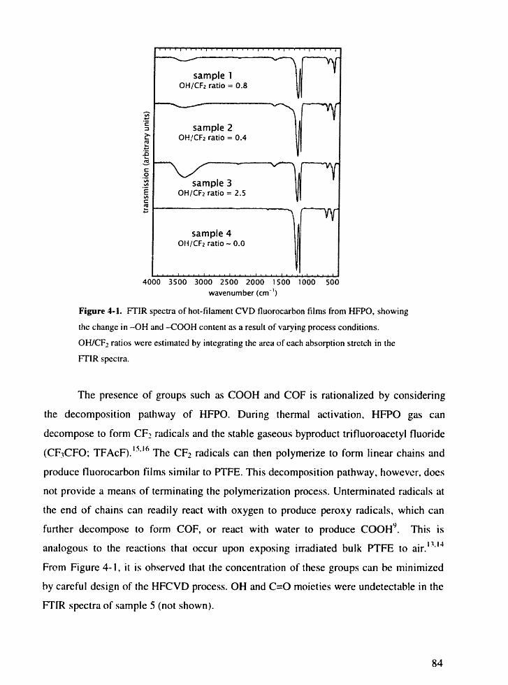
wavenumber (cm - ')
Figure 4-1. FTIR spectra of hot-filament CVD fluorocarbon films from HFPO, showing
the change in -OH and -COOH content as a result of varying process conditions.
OH/CF2 ratios were estimated by integrating the area of each absorption stretch in the
FTIR spectra.
The presence of groups such as COOH and COF is rationalized by considering
the decomposition pathway of HFPO. During thermal activation, HFPO gas can
decompose to form CF_ radicals and the stable gaseous byproduct trifluoroacetyl fluoride
(CF3CFO; TFAcF).' 1516 The CF 2 radicals can then polymerize to form linear chains and
produce fluorocarbon films similar to PTFE. This decomposition pathway, however, does
not provide a means of terminating the polymerization process. Unterminated radicals at
the end of chains can readily react with oxygen to produce peroxy radicals, which can
further decompose to form COF, or react with water to produce COOH9. This is
analogous to the reactions that occur upon exposing irradiated bulk PTFE to air. .4
From Figure 4-1, it is observed that the concentration of these groups can be minimized
by careful design of the HFCVD process. OH and C=O moieties were undetectable in the
FTIR spectra of sample 5 (not shown).
84

Exposure and Development. The films examined in Figure 4-1 were exposed to
e-beam and developed using supercritical CO 2. Positive tone patterning was achieved as
shown in the contrast curves, Figure 4-2. Complete development was observed in sample
4 with a dosage of 6,000 gC/cm 2. Sample 5 also showed complete development at 6,000
gC/cm 2. Contrast for each sample in the series correlates qualitatively with the
concentration of OH and C=O species. It is observed that the lower the OH/CF, ratio, the
higher the contrast under e-beam exposure.
100x xx
' 80 -o x80 X0
A X
U 60 _ o
-o key 0N 40 · sample I AE 0 sample 2
° 20 X sample 3 AOA sample 4 00
10o2 10o3 4e-beam dose (C/cm2)
Figure 4-2. Contrast curves of samples 3, 4, 6, and 7. showing c-beam
sensitivity following SCF CO, development. Sample 4 developed
completely in positive-tone.
The high doses required for development suggest that the order-of magnitude
increase in sensitivity desired for appropriate lithographic processing will require an
explicit understanding of the contrast mechanism coupled with specific molecular design
of future films. Addition of moieties for chemical amplification at e-beam (and
eventually 157 nm) may also be necessary. An atomic force microscope image of .() pim
lines and spaces is shown in Figure 4-3. These 1.0 pm lines showed complete positive-
tone development with high contrast. Sub-micron lines/spaces of 0.25 [Im have also been
obtained. AFM of the films after e-beam exposure and prior to development indicated
that ablation was not responsible for the high contrasts observed. Rather. supercritical
CO, acts as a developing medium to remove the irradiated material.
85

5UU
0
-500
nm
0 2.00 4.00 6.00 8.00,gm
Figure 4-3. AFM image of 1.0 pm lines/spaces in sample 5. Left
image is a top-down view, right plot is a cross-section through the line
shown at left.
4.5 Conclusion
We have demonstrated successful patterning of 1.0 gm lines/spaces in
fluorocarbon CVD films using a novel patterning process. Ongoing work includes the
incorporation of moieties during the CVD process to improve sensitivity and resolution.
Acknowledgements. The authors of this paper would like to thank the Cornell
Nanofabrication Facility, MIT Lincoln Labs, the NSF/SRC Engineering Research Center
for Environmentally Benign Semiconductor Manufacturing, and the Semiconductor
Research Corporation. This work also supported by the DOE and made use of MIT
MRSEC Shared Facilities supported by the NSF (DMR-9400334).
4.6 References
. See for instance, MRS Bulletin, 22 (1997).
2. S. J. Limb, K. K. S. Lau. D. J. Edell. F. F. Gleason, and K. K. Gleason, Pa.mla: s Poltm.. 4, 21
(1999).
3. K. K. S. Lau and K. K. (;leason J. Fluorine C/hen.. 104, t) (2(XX)).
4. R. . Kunz. T. M. Bloomicein. ). iE. Hardy. R. B. (]Goodman, 1). K. I)owns, and J. Curtin. J.
Vac. Si. ic(lthnol. B., 17, 3267 ( 999).
5. N. Sundararalan, S. Yang. K. ()Oino. S. Vallyavcctll, J Wang, X. Zlhou, and C. K. ()ler. (irit.
Mater., 12, 4 (2X N)).
6. C. F1. Kirhy and M. A. McHugh. ('het. Rev.. 99. 565 ( 199().
86
<~~~~~~ , P L J-VIX L ~~~ I~~~r; i_ t~~~~~~~"
,,,
- I I I

7. H. Namatsu, K. Yamazaki, and K. Kurihara, Microelect. Eng., 46, 129 (1999).
8. K. K. S. Lau and K. K. Gleason, Mater. Res. Soc. Symp. Proc., 544, 209 (1999).
9. K. K. S. Lau, J. A. Caulfield, and K. K. Gleason, Chem. Mater., 12, 3032 (2000).
10. C. Y. Liang and S. Krimm, J. Chem. Phys., 25, 563 (1956).
11. R. E. Moynihan, J. Am. Chem. Soc., 81, 1045 (1959).
12. W. K. Fisher and J. C. Corelli, J. Polym. Sci., Polym. Chem. Ed., 19, 2465 (1981).
13. N. P. G. Roeges, A Guide to the Complete Interpretation of Ifrared Spectra of Organic
Structures, John Wiley & Sons, New York,, (1994).
14. W. Burger, K. Lunkwitz, G. Pompe, A. Petr, and D. Jehnichen, J. Appl. Polym. Sci., 48, 1973
(1993).
15. W. Mahler and P. R. Resnick, J. Fluorine Chen., 3, 451 (1973).
16. P. J. Krusic, D. C. Roe, and B. E. Smart, Isr. J. Chem., 39, 117 (1999).
87

ii
i
rl
:iiI
1:
iii, 1t
I
i11
:~~~~~~~~~~bY
.i'A)EC
~~sa ntiao in HFV A or>
Peurflurooctun Suloy lurd
HG Pryce Lews, JA Caulfield, and KK Gleason. submilted to Langmufr

5.1 Abstract
We have demonstrated the successful use of an initiator species in hot-filament
chemical vapor deposition (HFCVD) of PTFE thin films. The introduction of PFOSF in
small concentrations allows the enhancement of deposition rates, increased control over
film composition, and control over film morphology. Endcapping by CF3 groups is
possible, which may provide benefits such as enhanced thermal stability and higher
hydrophobicity for HFCVD films. Conversion of the PFOSF is high, and HFPO
utilization efficiency can be increased significantly. The generation of an initiator radical
via the pyrolysis of PFOSF may contribute to enhanced nucleation rates during film
growth. Initiation and/or nucleation is rate-limiting at low filament temperatures, and
mass transport limitations dominate at higher filament temperatures.
89

5.2 Introduction
Hot-filament chemical vapor deposition (HFCVD, also known as pyrolytic CVD),
offers the ability to tailor the chemistry of films with polymeric structure. 1-4 In particular,
HFCVD allows for more control over precursor fragmentation pathways than
conventional plasma-enhanced CVD (PECVD).3 HFCVD uses thermal activation in the
gas phase to generate reactive species5, and allows independent control of the substrate
temperature to be exercised. The latter characteristic differentiates HFCVD from
conventional thermal CVD, in which precursor breakdown temperature and substrate
temperature are identical. The control over reaction pathways available via HFCVD make
it possible to produce polymeric fluorocarbon films spectroscopically similar to
poly(tetrafluoroethylene) (PTFE) with the precursor hexalluoropropylene oxide (HFPO;
CF 3CF(O)CF 2).3 PTFE has many desirable properties, including a low refractive index
and dielectric constant, low coefficient of friction, excellent chemical resistance, and high
thermal stability.6-8 Thin films of PTFE offer advantages for applications as diverse as
optical coatings9, biopassivation coatings for implantable devices'", and interlayer
dielectrics (ILDs) in integrated circuits 12' 3 However, bulk PTFE's high melt viscosity
and poor solubility make it difficult to process into thin, conformal, and uniform films. 8
By contrast, HFCVD is capable of providing good control over film structure and
morphology on wide range of substrates, including those that are thermally sensitive or of
complex geometry.
Previously, we have reported on the characterization of films produced using this
process", and on progress made in understanding the deposition chemistry of HFPO
during HFCVD. 5 In this paper, we report on the effects of adding an initiator species,
perfluorooctane sulfonyl fluoride (PFOSF, CFi(CF,)7SO 2F), to the HFCVD process. As
in conventional polymer chemistry, the use of an initiator allows control over both
growth rates and chemical composition of the resulting polymeric film. The use of
PFOSF also allows further elucidation of the chemistry of this novel deposition process.
90
5.3 Experimental
Films were deposited on silicon wafer substrates in a custom built vacuum
chamber, as described previously.' 4 Thermal excitation was accomplished by resistively
heating 28 AWG Nichrome wire (80% Ni/20% Cr) strung on a filament holder. The
filament holder straddled a cooled stage on which the silicon wafer was placed. The
filament to substrate standoff was 1.0 cm. Pressure in the reactor was maintained at 1.0
Torr by a butterfly valve. Undiluted HFPO of 98% purity, donated by DuPont, was
metered and controlled by a mass-flow controller. PFOSF was vaporized in a heated
vessel and delivered through a needle valve to maintain flow rates of approximately 3
sccm, 6 sccm, and 11 sccm at three different valve settings. Experiments were performed
at these valve settings and HFPO flow rates of 78 sccm and 158 sccm to evaluate the
effect of the PFOSF/HFPO flow ratio on deposition rate. Filament temperature was
measured using an 2.2 gtm infrared pyromcter. For oxidized Nichrome, a spectral
emissivity of 0.85 was estimated from direct contact thermocouple measurements.
Temperatures were consistent from run to run and there was little variation in power
requirements for heating the wire. Films were deposited at filament temperatures ranging
from 435 °C to 580 C. A single filament array was preconditioned for 15 minutes at 510
°C and used for all runs. Substrate temperature was maintained below 40 °C by backside
water cooling. Deposition rates were monitored in situ using interferometry. A cycle
thickness of 2,500 Almin was calculated and confirmed by profilometry measurements.
Nuclear Magnetic Resonance (NMR) experiments were performed on a home-built
spectrometer tuned to 254.0 MHz for 9F detection. A Chemagnetics 3.2 mm double-
resonance solids probe was spun at 23 to 25 kHz to perform high-resolution Magic-Angle
Spinning (MAS). All spectral chemical shifts were referenced to CFCI 3. Other
experimental details have been described elsewhere.' 5 Atomic force microscopy (AFM)
was performed on a Digital Instruments Dimension 3000. Images were taken under
tapping mode with a standard etched silicon tip.
91

5.4 Results and Discussion
Deposition Rate. The addition of small quantities of PFOSF to the HFCVD
process increases deposition rates significantly, as indicated in Figure 5-1a. This
enhancement in deposition rate is sensitive to the ratio of PFOSF/HFPO for filament
temperatures between 465 C and 531 C. With PFOSF present, the deposition rate is also
found to be sensitive to filament temperature. In Figure 5-lb, deposition rates are plotted
in Arrhenius form for films deposited at PFOSF/HFPO ratios greater than 0.07. Two
kinetic regimes are observed, with the transition point occurring at a filament temperature
of about 470 C. Below this temperature, the deposition rate depends strongly on filament
temperature, and an apparent activation energy of 256 kJ/mole is estimated. Above this
temperature, the deposition rate is significantly less sensitive to temperature, and the
apparent activation energy is close to zero.
92

E
a.
C
a
v,
PFOSF/HFPO flow ratio (sccm/sccm)
T (C)
E
a-
o,0
I 10 1.15 1.20 125 130 1.35 1.40 1.45
10or, (10'3 K')
Figure 5-1. Deposition rates of HFCVD fluorocarbon films from PFOSF and HFPO.
showing the effect of a. adding PFOSF, and b. changing filament temperature. Trend
lines in Figure 5- a arc included for visual clarification. Figure 5- 1 b shows data for
PFOSF/HFPO ratios greater than 0.07, and is plotted in Arrhenius form. Regression fits
illustrate kinetic regimes above and below -470°C.
Nuclear Magnetic Resonance (NMR) Spectroscopy. To elucidate differences
in composition between films produced with and without PFOSF, solid-state 19F NMR
spectroscopy was performed on the films (Figures 5-2a and 5-2b). Assignments are made
from the literature.'5
93

-60 -80 -100 -120 -140 -160 -18019
F ppm
Figure 5-2. Nuclear Magnetic Resonance (NMR) spectra of a. HFCVD film from the
precursors HFPO and PFOSF, b. HFCVD film from the precursor HFPO with no
PFOSF, and c. bulk PTFE. Concentrations of CF,, CF,. and CF are shown in mol %.
As in bulk PTFE (Figure 5-2c), both films show a primary peak at -123 ppm
assigned to CFCF, CF2. The HFCVD films (Figures 5-2a and 5-2b), however, show a
shift at -84 ppm which is associated with the endgroup CF3 CF 2CF 2, and a corresponding
shift at -128 ppm from CF 3CF 2'CF 2. The HFCVD films also show evidence of CF' near
-156 ppm. No spectroscopic evidence was found indicating retention of the SO 2 group
from PFOSF. The concentrations of each of the moieties CF, CF 2, and CF, have been
tabulated in Figures 5-2a through 5-2c. The concentration of CF, in bulk PTFE is
typically on the order of 0.01 mol %. below NMR sensitivity.6 Films deposited from
HFPO with the addition of PFOSF have a higher CF, concentration than both bulk PTFE
and films deposited from HFPO alone.
94
l

Atomic Force Microscopy (AFM). The morphology of films produced with the
addition of PFOSF was investigated using Atomic Force Microscopy (AFM). Figure 5-3
shows the effect of filament temperature on films produced using a PFOSF/HFPO ratio
of 0.145. Anisotropic, rodlike grain morphologies are observed in the film deposited at a
filament temperature of 435 C (Figure 5-3a) and an RMS roughness of 47 nm is
calculated. The film deposited at a filament temperature of 580 °C (Figure 5-3c) shows
nodular morphology and is much smoother with an RMS roughness of 6 nm. A
roughness of 15 nrn was measured for the film deposited at 510 °C (Figure 5-3b). By
comparison, the underlying silicon wafer substrate has an RMS roughness of 0.5 nm.' 6
Previous work'7 has shown that films grown from HFPO at low deposition rates possess
high-aspect ratio grain structures similar to those observed in Figure 5-3c. Nodular
structures comparable to those observed in Figure 5-3a were observed at higher
deposition rates. Changes in morphology were attributed to competition between the rates
of nucleation and propagation during the HFCVD process.' 7 By this reasoning, growth of
films from PFOSF and HFPO at filament temperatures below 510 °C must be dominated
by nucleation and/or initiation pathways rather than propagation events.
95

-2.00 330.0 nm
165.0 r
-1.00
O 1.000
2.00iN
00 110.0 w
55.0 o
0.0
00
un
2.00 r-lSO.O
25.0 nr
0.0
1.00
00 1.00 2.00
Figure 5-3. Atomic Force micrographs showing the effect of filament temperature on the
morphology of HFCVD films from HFPO and PFOSF. Films were deposited at a
PFOSF/HFPO ratio of 0.145 and filament temperatures of a. 435C. b. 5 10 C. and c.
580C. RMS roughnesses are also si '-vn
96

Reaction Chemistry. The pyrolysis of PFOSF has been investigated by other
workers over a temperature range of 460 C to 550 C, comparable to the range of
filament temperatures used in our work. ' 8 ' 9 No activation energy was reported.
Conversion of the PFOSF was found to increase with temperature, and conversions of
greater than 90% were reported above 490 °C at all PFOSF flow rates considered.' 8
Observed products were perfluorinated straight chain molecules from C8 to C16. A free
radical mechanism was postulated to account for the formation of these products, with
CF3(CF) 6CF2- as the primary reactive species. Similar pyrolysis chemistry is expected to
occur in our HFCVD system, and the formation of this radical species may constitute an
initiation event analogous to that described in classical polymer chemistry. The diradical
species, CF2 (difluorocarbene), generated from the pyrolysis of HFPO would then
constitute the propagating species. The proposed polymerization scheme is illustrated in
Figure 5-4. Reaction () describes initiation via the pyrolysis of PFOSF. Reaction (2)
describes the generation of polymerizable species from the pyrolysis of HFPO5' 2° 22, and
reaction (3) is the propagation step. Termination can occur via reaction with an
oligomeric fragment or the initiator species, as illustrated in Reactions (4) and (5).
Initiation: CF3(CF 2)7SO 2F - CF 3(CF2)6CF2 - + SO2 + F. (1)
Monomer Generation: CF 3CF(O)CF2 -' CF2 : + CF3C(O)F (2)
Propagation: CF 3(CF2) 6CF2 + nCF2 : - CF3(CF 2) 6(CF2 )n- (3)
CF3(CF 2) 6(CF2).- + CF3(CF 2)6(CF2)m' - CF 3(CF2)n+m+ 2CF3 (4)Termination: {
CF;(CF 2)6(CF 2).. + CF3(CF2)6CF2. - CF3(CF 2)+ 13CF 3 (5)
Figure 5-4. Proposed polymerization mechanism for HFCVD using HFPO and PFOSF.
The postulated mechanism provides an explanation for the results observed in our
work. The enhanced deposition rate of the films from HFPO and PFOSF is consistent
with a mechanism in which PFOSF contributes to initiation. The sensitivity to PFOSF
flow rate shown in Figure 5-la suggests that initiation may be rate-limiting. However, the
sensitivity of deposition rate to filament temperature shown in Figure 5-lb indicates that
there exists two kinetic regimes over the range of temperatures studied. Below about 470
"C, initiation via the pyrolysis of PFOSF is the rate-controlling step. Indeed, the apparent
97
activation energy of 256 kJ/mole for this region is close to the reported C-S bond energy
of 272 kJ/mole. 2 3 Above 470 °C, the kinetics are dominated by mass transfer limitations,
and deposition rate is relatively insensitive to filament temperature. 24 In previous work,
the conversion of PFOSF at 470 C has been reported as greater than 90% for low flow
rates. 1'8 '9 The conversion was observed to reach a maximum of about 97 % at 530 °C, and
was almost independent of flow rate above 550 OC.18 This suggests that above 470 C,
initiation via reaction (1) is no longer limiting.
Initiation by pyrolysis of PFOSF is also evidenced by the higher CF3
concentrations observed in films deposited from both PFOSF and HFPO. These CF3
moieties originate from the initiator radical produced by reaction (1) and are incorporated
into PTFE chains as end groups during propagation and termination. When HFPO is used
without PFOSF, initiation and termination by CF3 groups is less likely, and films reveal
the presence of OH and CO/COO moieties due to the reaction of unterminated CF 2 chain
radicals with oxygen and moisture.i4 Carboxyl end groups are observed in
fluoropolymers produced using bulk processing methods, and are generally considered
deleterious and unstable.2 5' 27 CF3 end groups can impart properties desirable for many
applications, including thermal stability and hydrophobicity. 26 '28 The presence of the
PFOSF initiator radical thus provides a eans for selectively endcapping the PTFE
chains.
The morphological effect induced by filament temperature suggests that initiation
and nucleation may be related in our system. In previous work with only HFPO, it was
proposed that nucleation was rate-limiting at low deposition rates, and propagation rate-
limiting at higher deposition rates. 14 In our system, the initiation step is found to be rate-
limiting at low temperatures, and a rod-like morphology consistent with nucleation-
limited film growth is observed. Conversely, at high temperatures when initiation is no
longer limiting, nodular morphology is observed analogous to that observed for
propagation-limited film growth. The pyrolysis of PFOSF may thus constitute both an
initiation and a nucleation event. This may be due to a higher sticking coefficient for the
PFOSF initiator radical than for CF 2. Indeed, the sticking coefficient for higher
molecular-weight fluorocarbon radicals is expected to be higher than that for CF229,
which is typically on the order of 10 -4 to 10-3 in the absence of low-energy ion
98

bombardment.3 '3 ' The PFOSF initiator species may thus adsorb preferentially to the
substrate surface and enable film growth. It is significant that morphological control that
was previously available primarily by variation of filament condition and residence time
can now be implemented by adding a secondary nucleating species.
5.5 Conclusions
In conclusion, we have demonstrated the successful use of an initiator species in
HFCVD of fluorocarbon thin films. The introduction of PFOSF in small concentrations
allows the enhancement of deposition rates, increased control over film composition, and
control over film morphology. Endcapping by CF 3 groups is possible, which may provide
benefits such as enhanced thermal stability and higher hydrophobicity for HFCVD films.
Conversion of the PFOSF is high, and HFPO utilization efficiency can be increased
significantly. The generation of an initiator radical via the pyrolysis of PFOSF may
contribute to enhanced nucleation rates during film growth. Initiation and/or nucleation is
rate-limiting at low filament temperatures, and mass transport limitations dominate at
higher filament temperatures. The demonstration of PFOSF as an initiator species
validates the argument that many techniques relevant to classical polymer chemistry may
be applied to HFCVD.
Acknowledgments. We gratefully acknowledge the support of the NIH under
contract NO 1-NS-9-2323, and the NSF/SRC Engineering Research Center for
Environmentally Benign Semiconductor Manufacturing in funding this work. This work
also made use of the MRSEC Shared Facilities supported by the National Science
Foundation under Award Number DMR-9400334.
5.6 References
1. M. C. Kwan and K. K. Gleason, CVD, 3, 299 (1997).
2. S. J. Limb, K. K. S. Lau, D. J. Edell, E. F. Gleason, and K. K. Gleason, Plasmas Polym., 4, 21
(1999).
3. K. K. S. Lau and K. K. Gleason, J. Fluorine Chem., 104, 119 (2000).
99

4. H. G. Pryce Lewis, T. B. Casserly, and K. K. Gleason, submitted.
5. K. K. S. Lau, K. K. Gleason, and B. L. Trout, J. Chem. Phys., 113, 4103 (2000).
6. D. L. Kerbow, in Polymeric Materials Encyclopedia, J. C. Salamone, Editor, 9, p. 6884, CRC
Press, Boca Raton (1996).
7. S. V. Gangal, in Encyclopedia of Polymer Science and Engineering, Vol. 16, H. F. Mark, N. M.
Bikales, C. G. Overberger, G. Menges, and J. A. Kroschwitz, Editors, p. 577, John Wiley and
Sons, New York (1989).
8. J. Scheirs, in Polymeric Materials Encyclopedia, J. C. Salamone, Editor, 4. p. 2498, CRC Press,
Inc., Boca Raton (1996).
9. L. Martinu and D. Poitras, J. Vac. Sci. Technol. A, 18, 2619 (2000).
10. D. E. Ocumpaugh and H. L. Lee, in Biomedical Polymers, p. 101, Marcel Dekker, New York
(1971).
11. W. R. Gombotz and A. S. Hoffman, Crit. Rev. Biocompat., 4, 1 (1987).
12. T. Rosenmayer and W. Huey, Mater. Res. Soc. Symp. Proc., 427, 463 (1996).
13. K. K. S. Lau and K. K. Gleason, Mater. Res. Soc. Symp. Proc., 544, 209 (1999).
14. K. K. S. Lau, J. A. Caulfield, and K. K. Gleason, Chem. Mater., 12, 3032 (2000).
15. K. K. S. Lau and K. K. Gleason, J. Phys. Chem. B, 102, 5977 (1998).
16. C. B. Labelle and K. K. Gleason, J. Appl. Polym. Sci., 74, 2439 (1999).
17. K. K. S. Lau, J. A. Caulfield, and K. K. Gleason, J. Vac. Sci. Technol. A, 18, 2404 (2000).
18. M. Napoli, C. Fraccaro, A. Scipioni, R. Armelli, and M. Pianca, J. Fluorine Chem., 24, 377
(1984).
19. E. Traverso, Chem. Ind. (Lond.), 523 (1986).
20. P. B. Sargeant, J. Org. Chem, 35, 678 (1970).
21. W. Mahler and P. R. Resnick, J. Fluorine Chem., 3, 451 (1973).
22. R. C. Kennedy and J. B. Levy, J. Fluorine Chem., 7, 101 (1976).
23. R. T. Sanderson, Chemical Bonds and Bond Energy, 2nd ed., Academic Press, New York, (1976).
24. A. S. Grove, Physics and Technology of Semiconductor Devices, p. 7, Wiley, New York, NY.,
(1967).
25. Y. I. Matveev, A. A. Askadskii, I. V. Zhuravleva, G. L. Slonimskii, and V. V. Korshak.
Vysokomol. Soedin., Ser. A, 23, 2013 (1981).
26. W. B. Farnham, A. E. Feiring, B. E. Smart, and R. C. Wheland, WO Patent No. 9702300 (1997).
27. M. Pianca, E. Barchiesi, G. Esposto, and S. Radice, J. Fluorine Chem., 95, 71 (1999).
28. A. W. Adamson, Physical Chemistry of Surfaces, 6th ed., p. 368, Wiley, New York, NY, (1997).
29. S. Samukawa and T. Mukai, Thin Solid Films, 374, 235 (2000).
30. D. C. Gray, I. Tepermeister, and H. H. Sawin, in Proceedings of the 2nd International Conference
on Reactive Plasmas, p. unpublished (1994).
31. K. Teii, M. Hori, T. Goto, and N. Ishii, J. Appl. Phys., 87, 7185 (2000).
100

CHAPTER 6Hot-Wire Deposition (HWCVD) ofFluorocarbon and OrganosiliconThin FilmsKKS Lau, HG Pryce !.ewis, SJ Limb, MK Kwan, and KK Gleason, submitted toThin Solid Films
101
l _~_~
LHz- I e1_ -
.1
Iii
.I
:1
1,y
I

6.1 Abstract
Hot-wire or Hot-Filament Chemical Vapor Deposition (HWCVD or HFCVD)
affords the capability to synthesize fluorocarbon and organosilicon thin films. These two
classes of materials are of interest for a wide range of applications, including low
dielectric constant coatings for microelectronic interconnection, "dry" photoresists,
directly patternable dielectrics for lithographic production of integrated circuits,
insulating biomaterials for implantable devices with complex topologies and small
dimensions, low friction coatings, and semipermeable membranes. HWCVD from
hexafluoropropylene oxide (C3F6 0) dramatically reduces crosslink and defect
concentrations in fluorocarbon coatings, producing films which are spectroscopically
indistinguishable from bulk polytetrafluoroethylene (PTFE, TeflonTM). Organosilicon
films can be deposited from cyclic precursors such as octamethylcyclotetrasiloxane (D 4 )
at extremely high rates (>2 microns/min) by HWCVD. The bonding structure of
HWCVD organosilicon films is substantially different from both their plasma enhanced
chemical vapor deposition PECVD) counterparts and bulk siloxane polymers, such as
poly(dimethysiloxane) (PDMS).
102

6.2 Introduction
Both fluorocarbon and organosilicon films find extremely diverse applications
because of their unique electrical, chemical and surface properties. Fluorocarbon films
are currently being evaluated as dielectric interconnects in microelectronic circuits and as
passivation coatings in clinical devices. 2 Potential applications of organosilicon CVD
thin films include biocompatible coatings for medical implants3, semipermeable
membranes, integrated optical devices 5, dielectric films6, and abrasion and corrosion
resistant coatings7
HWCVD represents an alternative to plasma-enhanced chemical vapor deposition
(PECVD) for depositing both fluorocarbon 8 and organosilicon 9 thin films. Plasma
exposure is entirely eliminated by HWCVD, a process in which a fluorocarbon or
organosilicon gas is thermally decomposed over a hot surface while the substrate remains
cool. In HWCVD, substrate temperature and gas precursor breakdown temperature are
independently controlled. This is a distinct difference from conventional thermal CVD
which involves heating the susceptor on which the substrate is placed.
HWCVD overcomes some of the processing constraints of having a directly
heated substrate. The advantage of being able to achieve high temperature gas
decomposition, yet film deposition on a substrate at room temperature, is three-fold.
First, absorption limited deposition processes can be employed, since lower substrate
temperatures enhance such mechanisms. Second, temperature sensitive substrates can be
coated without difficulty, and film stresses due to temperature mismatch during and after
deposition can be eliminated. Finally, significantly higher filament temperatures can be
attained with low power consumption, permitting a more extensive range of CVD
chemistries to be explored.
In this paper, HWCVD of fluorocarbon and organosilicon thin films in our
laboratory8 -15 is reviewed.
6.3 Experimental
For the fluorocarbon films, undiluted hexafluoropropylene oxide (HFPO;
CF3CF(O)CF 2) was used as the precursor gas. Organosilicon thin films were grown from
103

octamethylcyclotetrasiloxarte, [(CH 3)2SiO]4, also known as D 4 from the commonly used
nomenclature of D for -(CH 3) 2SiO-. D4 is a monomer which is commonly used in the
base catalyzed, liquid phase ring-opening polymerization to PDMS.
Films were deposited onto silicon wafers by HWCVD in a custom built vacuum
chamber (Figure 6-1) having backside water cooling on the substrate. The filament to
substrate distance was maintained at 2.5 cm for the fluorocarbon films, and 1.0 to 1.5 cm
for the organosilicon films. Table 6-1 summarizes the other HWCVD process
parameters.
Figure 6-1. Schematic of the HWCVD Chamber. Showing gas inlet through upper
showerhead, pyrolysis on square filament array, and deposition onto a wafer substrate
resting on the bottom electrode. Gas pump out is toward the back side of the chamber.
Table 6-1. Typical process conditions for HWCVD.
CVD Parameter Fluorocarbon Organosilicon
Filament temperature (°C) 400 to 500 800 to 1000
Filament composition NiCr (80%/20%) Ta
Substrate temperature (C) 25 25
Pressure (torr) 0.4 to 1.2 0.2 to 1.0
Flow rate (sccm) 10 to 40(X) 1 to 15
Feed gas HFPO D4
104

X-ray photoemission (XPS) survey and Cls scans were obtained at a takeoff
angle of 45 ° using a Mg Ka 1, 2 source on a Perkin Elmer 5100 instrument. Two spectra
were run, a high resolution Cls and a low resolution (e survey) over a broader energy
range. A Nicolet 860 was used to obtain the Fourier transform infrared (FTIR) spectra.
High-resolution solid-state nuclear magnetic resonance (NMR) experiments were
performed with a Chemagnetics 3.2 mm magic angle spinning probe at a field of 6.3
Tesla.
6.4 Results and Discussion
Figures 6-2 and 6-3 compare the 19F NMR and FTIR spectra, respectively, for a
film grown by HWCVD of HFPO to bulk PTFE, showing the similarity in chemical
structure of the two types of materials.
Figure 6-2. Solid
ppm 0 -100
state '9F NMR of HWCVD
-200 -300
fluorocarbon film (bottom) and PTFE (top).
bulk PTFE
1,,,I .... I .... I .... I......I.,I....,I....lI ...
105

4000 3500 3000 2500 2000 1500 1000 500wavenumber (cm -')
Figure 6-3. FTIR of HWCVD fluorocarbon film (bottom) and PTFE (top).
The precursor gas HFPO has a well-known thermal decomposition pathway
(Figure 6-4), which commences at a fairly low temperature of 150°C. 16
CF3 CF CF2 ; CF2 + CF3 CF0 0
:CF2 - (CF2CF2)-
Figure 6-4. Reactions for the pyrolysis of HFPO and
polymerization of difluorocarbene.
The product, difluorocarbene, can then polymerize to form linear CF 2 chains.'3
Thus, HWCVD fluorocarbon films differ from their counterparts grown by PECVD. The
PECVD films generally have a F/C ratio of -1.5 as compared to 2 for PTFE [-(CF2)-]. In
addition, the PECVD films contain dangling bonds (free radicals), double bonds and
crosslinks. These defects degrade the film electrical and mechanical properties, and also
contribute to the aging of these materials.' 7 Exposure of the growth surface to the plasma
plays a key role in defect formation. Plasma exposure is entirely eliminated by HWCVD.
Using HWCVD from D4, high deposition rates (up to 2.5 pm/min) for
organosilicon thin films could be achieved. 9 FTIR (Figure 6-5) verified that the deposited
films had the same functional groups as a poly(dimethylsiloxane) (PDMS) standard,
106

though with a measurably lower methyl concentration. Marked differences in the IR
intensity can be seen at 2964 cm - ' (asymmetric methyl stretch), 2906 cm -' (symmetric
C-H methyl stretch), and at 1410 cm - ' (C-H methyl bending modes). No C-C crosslinking
is detected, since such a rearrangement would result in the appearance of new peaks in
the C-H stretch region at lower wavenumbers corresponding to sp3-CH 2. Such sp3-CH 2
peaks are often observed in PECVD films. 18 Thus, the HWCVD materials differ from
both PDMS and PECVD films.
-.,
a
V:._
-0.0
4000 3500 3000 2500 2000 1500 1000 500
wavenumber (cm- ')
Figure 6-5. FTIR of HWCVD organosilicon film (top) and PDMS (bottom).
XPS showed that a typical film had an elemental composition of C:Si:O / 1.5: 1:1,
confirming the loss of methyl groups. 29Si NMR suggested the existence of Si-Si
crosslinking in the film, also consistent with the loss of methyl groups.'5
The ability of HWCVD to extend the compositional range beyond that of PECVD
films can ultimately improve the resulting properties. The molecular architectures
uniquely achieved by HWCVD enable all-dry, resistless patterning of fluorocarbon low
dielectric constant films, using supercritical CO2 as the development medium. 19 Lines
and spaces defined by electron beam lithography at 0.25 micron resolution are shown in
Figure 6-6.
107

Figure 6-6. HWCVD fluorocarbon low dielectric
constant film directly patterned at 1.0 (left) and 0.25
(right) micron resolution.
In addition, the absence of plasma driven densification processes can lead to the
incorporation of porosity in the HWCVD films, further reducing their effective dielectric
constant.14 Under HFCVD conditions which limit nucleation, a unique morphology can
arise in HWCVD fluorocarbon films, as shown in Figure 6-7. This morphology clearly is
the source of the porosity.
Figure 6-7. Scanning electron micrograph of HWCVD porous
fluorocarbon film at the edge of the silicon wafer substrate (bottom
right). The tilt angle makes it possible to observe both the surface
morphology (top left) and porosity through the thickness of the layer.
108
a:5:1 I:

6.5 Conclusions
Fluorocarbon films have been deposited by HWCVD and possess a chemical
structure siriiar to poly(tetrafluoroethylene). Organosilicon films can be deposited from
cyclic precursors such as octamethylcyclotetrasiloxane (D4) at extremely high rates (>2
microns/min) by HWCVD. The bonding structure of HWCVD organosilicon films is
substantially different from both their PECVD counterparts and bulk siloxane polymers,
such as poly(dimethylsiloxane).
In contrast to PECVD, the HWCVD process does not involve any ion
bombardment or UV irradiation, thus eliminating the possibility of related atomic
rearrangements and defects. The ability to grow fluorocarbon and silicone thin films by
hot wire CVD reveals that ion bombardment, which is often cited in discussions of
PECVD mechanisms as being essential to the creation of active sites for film growth20, is
in fact not necessary for the deposition of these materials.
Acknowledgements. We gratefully acknowledge the NIH (Contract NOI-NS-3-
2301), NSF (CTS-9057119) and the NSF/SRC Engineering Research Center for
Environmentally Benign Semiconductor Manufacturing for funding this work. This work
made use of MRSEC Shared Facilities supported by the NSF (DMR-9400334).
6.6 References
1. K. Endo, T. Tatsumi, Y. Matsubara, and T. Horiuchi, Jpn. J. Appl. Phys., Pt. 1, 37, 1809 (1998).
2. B. D. Ratner, A. Chilkoti, and G. P. Lopez, in Plasma Deposition, Treatment, and Etching of
Polymers, R. d'Agostino, Editor, p. 463, Academic Press, San Diego, CA (1990).
3. A. S. Chawla, Biomaterials, 2. 83 (1981 ).
4. J. Sakata and M. Yamamoto, J. Appl. Polym. Sci., Appl. Poym. Symp., 42, 339 (1988).
5. P. K. Tien, Rev. Mod. Phys., 49, 361 (1977).
6. M. R. Wertheimer and T. S. Ramu, US Patent No. 4599678 (1986).
7. T. Wydcven, Appl. Opt., 16, 717 (1977).
8. K. K. S. Lau and K. K. Gleason, J. Fluorine Chem., 104, 119 (2000).
9. M. C. Kwan and K. K. Gleason, CVD, 3, 299 (1997).
109

10. S. J. Limb, C. B. Labelle, K. K. Gleason, D. J. Edell, and E. F. Gleason, Appl. Phys. Lett., 68,
2810 (1996).
11. S. J. Limb, K. K. S. Lau, D. J. Edell, E. F. Gleason, and K. K. Gleason, Plasmas Polym., 4, 21
(1999).
12. K. K. S. Lau, J. A. Caulfield, and K. K. Gleason, Chem. Mater., 12, 3032 (2000).
13. K. K. S. Lau, K. K. Gleason, and B. L. Trout, J. Chem Phys., 113, 4103 (2000).
14. K. K. S. Lau, J. A. Caulfield, and K. K. Gleason, J. Vac. Sci. Technol. A, 18, 2404 (2000).
15. H. G. Pryce Lewis, T. B. Casserly, and K. K. Gleason, submitted.
16. H. Millauer, W. Schwertfeger, and G. Siegemund, Angew. Chemn, 97, 164 (1985).
17. H. Yasuda, J. Macromol. Sci. - Chem., A10, 383 (1976).
18. H. G. Pryce Lewis, D. J. Edell, and K. K. Gleason, Chem. Mater., 12, 3488 (2000).
19. G. L. Weibel, H. G. Pryce Lewis, K. K. Gleason, and C. K. Ober, Polym. Prepr., 41, 1838 (2000).
20. A. M. Wr6bel and M. R. Wertheimer, in Plasma Deposition, Treatment, and Etching of Polymers,
R. d'Agostino, Editor, p. 163, Academic Press, San Diego, CA (1990).
110

CHAPTER 7Conclusions and Future Work
111
I
- "= =··l-CI
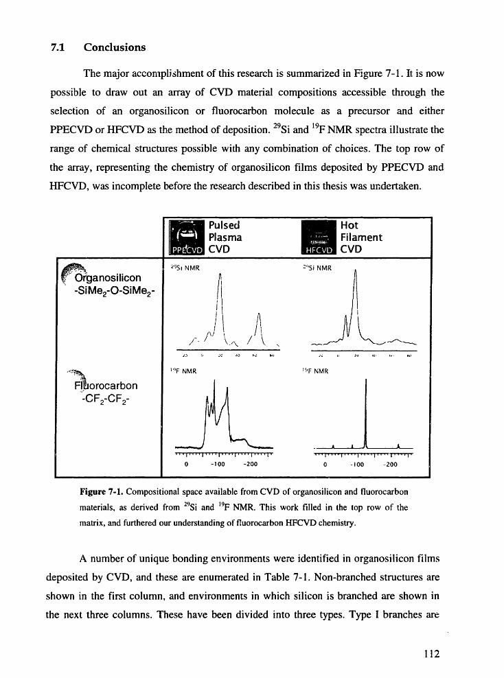
7.1 Conclusions
The major accomplishment of this research is summarized in Figure 7-1. It is now
possible to draw out an array of CVD material compositions accessible through the
selection of an organosilicon or fluorocarbon molecule as a precursor and either
PPECVD or HFCVD as the method of deposition. 29Si and 19F NMR spectra illustrate the
range of chemical structures possible with any combination of choices. The top row of
the array, representing the chemistry of organosilicon films deposited by PPECVD and
HFCVD, was incomplete before the research described in this thesis was undertaken.
Figure 7-1. Compositional space available from CVD of organosilicon and fluorocarbon
materials, as derived from 29Si and '9F NMR. This work filled in the top row of the
matrix, and furthered our understanding of fluorocarbon HFCVD chemistry.
A number of unique bonding environments were identified in organosilicon films
deposited by CVD, and these are enumerated in Table 7-1. Non-branched structures are
shown in the first column, and environments in which silicon is branched are shown in
the next three columns. These have been divided into three types. Type I branches are
112

typical of organosilicon materials prepared by conventional methods such as anionic
polymerization.' They were observed in PECVD films from D3, but were present only in
low concentrations in HFCVD films. Type II branches involve methylene bonds between
siloxane units, and were unique to PECVD films deposited from D3 under continuous
excitation. Type III branches consist of silicon-silicon bonds between siloxane units, and
were observed in HFCVD films grown from D3 and D4. The proximity of these silicon-
silicon bonds to siloxane bonds is remarkable, and probably the result of the
incorporation of siloxane ring species in the film structure. HFCVD is thus capable of
retaining much of the organic structure present in the precursor molecule.
Table 7-1. Silicon bonding environments in PPECVD and HFCVD organosilicon films.
Non- TYPE TYPE TYPEBranched I11 111
CH3 ?.~ CH3 / CH3I I I-°h-Si-CH3 _-1 Si- O Sii-0 CH3-Si- Si-'
CH3 CH, (CH2).x o CH 3
EF 1 ' E [ DCH2 | | DM lI I I I
CH3 , (CH,2 ). O° OI I I I I
-0o,- -os-o3' - oS- si-o.r CH-Si-c.,CH3 , (CH2). O1 O!Y
Oy,
-o,- Si- o-(CH2) L-~ITCHx21
note: x = or 1
A better understanding of the HFCVD chemistry of fluorocarbon thin films was
also obtained, and we have demonstrated the use of an initiator species to control
polymerization rates and influence film composition. We believe the latter result is
113

particularly novel and unique, and constitutes a significant contribution to our
understanding of the possibilities of gas-phase chemistry processes such as HFCVD.
7.2 Future Work
I believe this research should proceed primarily in the direction of:
Development of new HFCVD materials. HFCVD has already proved itself as a
powerful technique capable of producing fluorocarbon and organosilicon materials of
unique composition and structure. This technique should be extended to new polymeric
systems. The ability to produce polymeric materials on substrates of small and complex
geometry will be a key enabler for many emerging technologies in optics, micro-electro
mechanical systems (MEMS), and biomedical applications. This also has application for
Direct Dielectric Patterning, where new materials of greater sensitivity to e-beam and
157-nm irradiation are required to prove viability and expedite integration of the process
in the microelectronics industry.
7.3 References
1. W. Noll, Chemistry and Technology of Silicones, 2nd ed., Academic Press, New York, (1968).
114

iiI
II
11
1 ~
lill APElDIX A
Reactor Design andConstruction
II
i
ri
iIfLIi
II
115
3Z -- -- :- _=: _
A: 1II 1 U I l
il
; i

A.1 Description
A new CVD reactor system was built, and is shown in Figure A-1. The system
was designed to operate in both PPECVD and HFCVD modes, and has a water-cooled
stage on which substrates are placed during deposition. A single mechanical pump was
used to sustain vacuum pressures down to about 30 mTorr. Flow into the chamber is
controlled in two ways: volatile feeds are metered through a flow distribution manifold
located in the hood and enter the chamber through the top o-ring sealed port; low vapor-
pressure feeds are metered through an MKS 1153 heated mass-flow controller located at
the rear of the reactor and enter through a Con-Flat (CF, or Del-Seal®) flange at the rear
of the chamber. An access door is located at the front of the chamber, which allowed
visual inspection of the deposition process for the first time. Film deposition rates can be
measured in situ using an interferometry system, and filament temperature can be
monitored during HFCVD by a pyrometer operating at a wavelength of 2.2-micron. Up to
500W RF power (at 13.56 MHz) is available for PPECVD applications, and a pulse
generator can be used to modulate on- and off-times. DC power is available for filament
heating.
Figure A-1. Photographs of the dual-mode CVD reactor system known as Pumpkin.
116

Front, rear, top and side views of the main chamber are shown in Figures A-2
through A-4. These views show the positions of various ports and the features of the
reactor lid. All dimensions are in inches.
REARVIEW
organosilicon precursorfeed port (rear flange)
m rm ra
W ELir
LLU
Figure A-2. Front and rear view of chamber, showing feed port
TOP precursor'k Fir-% AI It feed poit
· 11Iril/
V t
4-
and pumping port.
Figure A-3. Top view of chamber, showing lid design, and filament orientation for HFCVD.
117
FRONTVIEW
. ' .
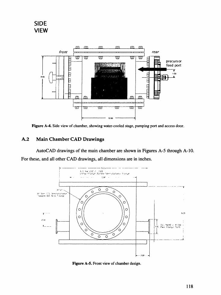
SIDEVIEW
rn m rrn rm r rnfront - .
WiJJ WU WJ LLU W
, o1000 -
Figure A-4. Side view of chamber, showing water-cooled stage, pumping port and access door.
A.2 Main Chamber CAD Drawings
AutoCAD drawings of the main chamber are shown in Figures A-5 through A-10.
For these, and all other CAD drawings, all dimensions are in inches.
ir; \; Fc .' ]3 icL rrr;l -e ;l PI,) t.> teso',:--"lt- L'. ! ,
I -.-d-1:I,
! .....-<i 1:)C
-- (>r L
Figure A-5. Front view of chamber design.
118
rear
I ,8 O I
I C
]3
I1 I E
_ I
precursorfeed portI
I
szipil J
_ I l _
rag i- .· ·
i -.--.
I
.

I
Figure A-6. Front view of chamber design, rotated 30 ° clockwise as observed from above.
/ :-It.
/ : ,r ' 1,4C , K3',vk cr e 'c rt
Figure A-7. Front view of chamber design, rotated 60° clockwise as observed from above.
i1 .......
b' '", .1 Nrror ta. ClT,, ,, --fo! ii orr1
i...
i.
Figure A-8. Front view of chamber design, rotated 90° clockwise as observed from above.
119

8' Non O.D. NonrotatblteTapped Del-Seal Flange
LOO000BotltedFloange
NW50 / K200-Fange Ported)
ISO NW40 / K150Kwik-Flange Port
/ K150e Port
8' Non OD. NonrototableTapped Del-Seal Fange
Figure A-9. Top view of chamber design, showing position of ports.
Figure A-10. Assembly view of main chamber design.
120
ISO NW40 / Kvik-Flange F
ISO NW5Kw*k-Fo(Anged)

A.3 Bottom Plate CAD Drawing
The original design for the bottom plate is shown in Figure A-il. Upon the
recommendation of MDC Vacuum, Inc., the copper tubing was replaced with a stainless
steel plate -in. below the top of the stage to create a cooling water reservoir beneath the
stage. Inlet and outlet tubing was welded into the reservoir.
_ -_ 3
FMMF~~W/zj
-- ---- …
.'I 4'' o
WA t-watc F
r <God r u-W t (-
f It'7]E·, "
),c Tsio!,
dr ho-: I * z~ -n -. I,e = --d-;H '.
]i
_ L _I
I· , .
.7J _-'-- - - _
'::at - gr1',) 4,('
Figure A- 1. Side cutaway view of original design of bottom plate. Note that copper tubing was replaced
with a stainless steel reservoir -in. deep with inlet and outlet tubing in final construction.
A.4 Reactor Lid CAD Drawings
The reactor lid was designed to facilitate the use of a feedthrough Teflon tube to
hold the showerhead during PPECVD applications. A central o-ring seal was designed
for this purpose. /4-in. VCR fittings and NW16 ports were also provided for gas feeds
and electrical/thermocouple feedthroughs. AutoCAD drawings are shown in Figures A-
12 through A-14.
121
- o w - -ow -S --so -o - -fin -------- of of on # To f ''A'S'o'fi' outdo' I____ 1
i) Y� l

CAJDN !/4' V:jRCcnec-t ror
ISI NW:i / YC. 5<wk-Fnige Prtr
-- C3 --
Figure A-12. Side view of reactor lid, showing '/4-in. VCR and NW16 ports.
:S- 'U . / YU7"
Figure A-13. Side cutaway view of reactor lid, showing /2-in. o-ring port and NW 16 ports.
/ LO000ge Boltedle Btonk
etelded! VCR LPorts
Figure A-14. Top view of reactor lid, showing all ports.
122
IS-,f -
-3.7
I'X'] , W16 / K\,W ?I .. 1.; . - . 9 A_
... £
CAPI --N I/P' -loc
A- '3fC ~ oreiL? ;lr UC(
r' l
. .... . . .

A.5 Rear Flange CAD Drawings
A rear flange was designed to accommodate extra feedthrough and feed ports.
The 2-3/4-in. CF port was used as the feed port for low vapor-pressure precursors
delivered through the MKS 1153 mass flow controller.
SIDE CUTAWAY VIEW OF PORTED FLANGE
1/4" CAJON VCR2-3/4' OD Del/Seai Flush Mounted should be sameon 8' Flange. Nonrnal ID o 2-3/4' height as 1/2"
Flange should be 1-3/4'. VCR
holes on 2-3/4' flange.-1 ,,000
Through ho/es on 8' angeI
8' OD Del-Seal/CFFtange. Rotatablew/ Through Holes
SEECUTAWAYABOVE
00.25Topped hole
2-3/4' DeNon-r
with TappedNominal
holes
2.00
2.00
VCR ort
1.50 1 50
TOP VIEW OF PORTED FLANGE
Figure A-15. Top and side views of rear flange.
123
Topped
U,a)U
C
C
0U,Cii,E)E'0
I'I
APPENDIX BAdditive Precursors Used inCombination with HFPO HFCVD
124
�I
I ---- --- -------

B.1 List of Additive Precursors
Table B-1 lists the precursors that were used in combination with HFPO in a
screening program designed to test the effects of adding a secondary species during
HFCVD. The incorporation of sulfone moieties was desired to increase the e-beam and
157-nm irradiation sensitivity of the basic fluorocarbon materials.
Table B-I. Precursors used in combination with HFPO HFCVD.
Desired Moiety Secondary precursor Structure
tetramethylene sulfone
sulfolane o ,o
perfluoroctane sulfonyl fluoride oCF,(CF,),CF,- S- FPFOSF
SULFONE dimethyl sulfone o
DMSO 2 c-cO
trifluoromethane sulfonic anhydride o oTFMSA F,C-S-O-S-CF,
i~~~~~~~~~~lb
B.2 Deposition Rates with Additive Precursors
The addition of secondary species during HFPO HFCVD was found to increase
deposition rates significantly, as illustrated in Figure B-1. This was attributed to the effect
of initiation as described in Chapter 5 of this work.
125

1ZUUU- 10,61 5 A/min
8,120
4,050 A/min
300 A/min
Hif P)no additive
625 A/min0im9l ~
fDMSrDMSO2
H F O HFPOsulfolane PFOSF
Figure B-1. Typical deposition rates obtained using HFPO with secondary precursor species.
B.3 New Chemistries Possible Using HFCVD with Dual Precursors
Selective endcapping of PTFE chains using HFCVD was demonstrated using
HFPO and dimethyl sulfone together, as shown in the Cls XPS spectra in Figure B-2.
294 289 284 279 274
BE(eV)
Figure B-2. Cls XPS spectra showing high surface concentrations of
terminal CH 3 groups in PTFE films
126
1000C
E
Ca
o._oQ0a.,
800O
6000
4000
2000
0f
HFI ,OTFMSA
__ _1______�1__��_ _II_____ · ___ ______ ______ ___I__ ___
l
=J&Iaf��'^^^^
I I
i
i
11I

These results suggest that HFCVD is a powerful technique for producing CVD
films of novel composition. A more extensive investigation into the potential for
development of materials that can be customized for specific applications is warranted.
127

THESIS PROCESSING SLIP
name
index biblio
· COPIES: (Archives;
Lindgren
TITLE VARIES: ,-
Aero
Music
Dewey
Rotch
, Hum
•cience) Sche-Plough
NAME VARIES: ____ ._-_;_. X X X_ /
IMPRINT: (COPYRIGHT)
· COLLATION:
* ADD: DEGREE: ') EPT.:
· ADD: DEGREE: * · DEPT.:
SUPERVISORS:
NOTES:.11 It
/
cat'r;-"
*DEPT: '. ;v.) L
*- YEAR: 27 t -- DEGREE:
NAME: K- I / LIhV644*1 ~~~~~~~~~~~~~~~~,-'
f
., .a
\
date:page:
~ \!-Ji
LE /y i _ . 'jI?- ;
FIXED FIELD: ill.
- ~ ~ ~ ~ -
. .
iiirl
-
·-
"--"- -- -' _,--