circuit components introduction and simulation...
TRANSCRIPT

Advanced Design System 2001
Circuit ComponentsIntroduction and Simulation Components
August 2001

Notice
The information contained in this document is subject to change without notice.
Agilent Technologies makes no warranty of any kind with regard to this material,including, but not limited to, the implied warranties of merchantability and fitnessfor a particular purpose. Agilent Technologies shall not be liable for errors containedherein or for incidental or consequential damages in connection with the furnishing,performance, or use of this material.
Warranty
A copy of the specific warranty terms that apply to this software product is availableupon request from your Agilent Technologies representative.
Restricted Rights Legend
Use, duplication or disclosure by the U. S. Government is subject to restrictions as setforth in subparagraph (c) (1) (ii) of the Rights in Technical Data and ComputerSoftware clause at DFARS 252.227-7013 for DoD agencies, and subparagraphs (c) (1)and (c) (2) of the Commercial Computer Software Restricted Rights clause at FAR52.227-19 for other agencies.
Agilent Technologies395 Page Mill RoadPalo Alto, CA 94304 U.S.A.
Copyright © 2001, Agilent Technologies. All Rights Reserved.
ii

Contents1 Introduction
BinModel (Bin Model for Automatic Model Selection)............................................... 1-2DataAccessComponent (Data Access Component)................................................. 1-6FORMAT A, B, C, D, E (Drawing Formats) ............................................................... 1-12Ground (Ground Component)................................................................................... 1-13Port (Port Component) ............................................................................................. 1-14Term (Port Impedance for S-parameters) ................................................................. 1-15VAR (Variables and Equations Component)............................................................. 1-16Multiplicity ................................................................................................................. 1-24Components from Product Migration........................................................................ 1-26
Component Categories ...................................................................................... 1-26
2 Lumped ComponentsC (Capacitor) ............................................................................................................ 2-2C_Model (Capacitor Model)...................................................................................... 2-4C_Conn (Capacitor (Connector Artwork)) ................................................................ 2-5C_Pad1 (Capacitor (Pad Artwork)) ........................................................................... 2-6C_Space (Capacitor (Space Artwork)) ..................................................................... 2-7CAPP2_Conn (Chip Capacitor (Connector Artwork))............................................... 2-8CAPP2_Pad1 (Chip Capacitor (Pad Artwork)) ......................................................... 2-10CAPP2_Space (Chip Capacitor (Space Artwork)) ................................................... 2-12CAPQ (Capacitor with Q) ......................................................................................... 2-14CQ_Conn (Capacitor with Q (Connector Artwork)) .................................................. 2-16CQ_Pad1 (Capacitor with Q (Pad Artwork)) ............................................................. 2-18CQ_Space (Capacitor with Q (Space Artwork)) ....................................................... 2-20DC_Block (DC Block) ............................................................................................... 2-22DC_Feed (DC Feed)................................................................................................. 2-23DICAP (Dielectric Laboratories Di-cap Capacitor).................................................... 2-24DILABMLC (Dielectric Laboratories Multi-Layer Chip Capacitor) ............................. 2-26INDQ (Inductor with Q) ............................................................................................. 2-28L (Inductor) ............................................................................................................... 2-30L_Conn (Inductor (Connector Artwork)) ................................................................... 2-32L_Model (Inductor Model.......................................................................................... 2-33L_Pad1 (Inductor (Pad Artwork)) .............................................................................. 2-34L_Space (Inductor (Space Artwork)) ........................................................................ 2-35LQ_Conn (Inductor with Q (Connector Artwork)) ..................................................... 2-36LQ_Pad1 (Inductor with Q (Pad Artwork)) ................................................................ 2-38LQ_Space (Inductor with Q (Space Artwork)) .......................................................... 2-40Mutual (Mutual Inductor)........................................................................................... 2-42PLC (Parallel Inductor-Capacitor)............................................................................. 2-44
iii

PLCQ (Parallel Inductor-Capacitor with Q)............................................................... 2-45PRC (Parallel Resistor-Capacitor) ............................................................................ 2-47PRL (Parallel Resistor-Inductor) ............................................................................... 2-48PRLC (Parallel Resistor-Inductor-Capacitor)............................................................ 2-49R (Resistor) .............................................................................................................. 2-50R_Model (Resistor Model)........................................................................................ 2-52R_Conn (Resistor (Connector Artwork)) .................................................................. 2-54R_Pad1 (Resistor (Pad Artwork)) ............................................................................. 2-55R_Space (Resistor (Space Artwork)) ....................................................................... 2-56Short (Short)............................................................................................................. 2-57SLC (Series Inductor-Capacitor) .............................................................................. 2-58SLCQ (Series Inductor-Capacitor with Q) ................................................................ 2-59SMT_Pad (SMT Bond Pad) ...................................................................................... 2-61SRC (Series Resistor-Capacitor).............................................................................. 2-63SRL (Series Resistor-Inductor)................................................................................. 2-64SRLC (Series Resistor-Inductor-Capacitor) ............................................................. 2-65TF (Transformer)....................................................................................................... 2-66TF3 (3-Port Transformer) .......................................................................................... 2-67
3 Miscellaneous Circuit ComponentsCAPP2 (Chip Capacitor)........................................................................................... 3-2CIND (Ideal Torroidal Inductor)................................................................................. 3-4RIND (Rectangular Inductor) .................................................................................... 3-5XFERP (Physical Transformer)................................................................................. 3-7XFERRUTH (Ruthroff Transformer).......................................................................... 3-9XFERTAP (Tapped Secondary Ideal Transformer) ................................................... 3-11
4 Probe ComponentsCounter (Counter Component) ................................................................................. 4-2I_Probe (Current Probe) ........................................................................................... 4-3OscPort (Grounded Oscillator Port).......................................................................... 4-4OscPort2 (Differential Oscillator Port)....................................................................... 4-7OscTest (Grounded Oscillator Test).......................................................................... 4-14TimeDelta (Time Delta Component)......................................................................... 4-15TimeFrq (Time Frequency Component).................................................................... 4-17TimePeriod (Time Period Component) ..................................................................... 4-18TimeStamp (Time Stamp Component)..................................................................... 4-19WaveformStats (WaveformStats Component) .......................................................... 4-20
5 Simulation Control ItemsSimulation Parameters: DC ...................................................................................... 5-1
Sweep................................................................................................................. 5-2Parameters ......................................................................................................... 5-3
iv

Display................................................................................................................ 5-7Simulation Parameters: AC....................................................................................... 5-8
Frequency........................................................................................................... 5-8Noise .................................................................................................................. 5-8Parameters ......................................................................................................... 5-10Output................................................................................................................. 5-10Display................................................................................................................ 5-10
Simulation Parameters: S_Param............................................................................. 5-11Frequency........................................................................................................... 5-11Parameters ......................................................................................................... 5-11Noise .................................................................................................................. 5-12Output................................................................................................................. 5-13Display................................................................................................................ 5-13
Simulation Parameters: HB ...................................................................................... 5-14Freq .................................................................................................................... 5-15Sweep................................................................................................................. 5-15Params ............................................................................................................... 5-15Small-Sig ............................................................................................................ 5-18Noise (1) ............................................................................................................. 5-18Noise (2) ............................................................................................................. 5-19NoiseCons.......................................................................................................... 5-21Osc ..................................................................................................................... 5-22Solver ................................................................................................................. 5-22Output................................................................................................................. 5-24Display................................................................................................................ 5-24
Simulation Parameters: LSSP .................................................................................. 5-29Ports ................................................................................................................... 5-29
P2D Simulation......................................................................................................... 5-29Simulation Parameters: XDB .................................................................................... 5-30
Freq .................................................................................................................... 5-30X dB.................................................................................................................... 5-30Params ............................................................................................................... 5-30Solver ................................................................................................................. 5-31Output................................................................................................................. 5-31Display................................................................................................................ 5-31
Simulation Parameters: Circuit Envelope ................................................................. 5-32Env Setup ........................................................................................................... 5-32Env Params ........................................................................................................ 5-33HB Params ......................................................................................................... 5-35Small-Sig ............................................................................................................ 5-36Noise(1) .............................................................................................................. 5-36Noise(2) .............................................................................................................. 5-36
v

Output................................................................................................................. 5-36Display................................................................................................................ 5-36
Simulation Parameters: Tran .................................................................................... 5-37Time Setup ......................................................................................................... 5-37Integration........................................................................................................... 5-38Convolution......................................................................................................... 5-40Convergence ...................................................................................................... 5-42Options ............................................................................................................... 5-44Noise .................................................................................................................. 5-45Freq .................................................................................................................... 5-46Output................................................................................................................. 5-47Display................................................................................................................ 5-47
Options Component.................................................................................................. 5-48Misc .................................................................................................................... 5-48Convergence ...................................................................................................... 5-48Output................................................................................................................. 5-50DC Solutions ...................................................................................................... 5-50Display................................................................................................................ 5-51
Sweep Plan Component........................................................................................... 5-52Parameter Sweep Component ................................................................................. 5-53
Sweep Tab.......................................................................................................... 5-53Simulations Tab .................................................................................................. 5-54Display Tab ......................................................................................................... 5-54
Budget Linearization................................................................................................. 5-55Using the BudLinearization Component............................................................. 5-55
Noise Component..................................................................................................... 5-56NoiseCon Freq Tab............................................................................................. 5-56NoiseCon Nodes Tab.......................................................................................... 5-56NoiseCon Misc Tab............................................................................................. 5-57NoiseCon PhaseNoise Tab................................................................................. 5-59NoiseCon Display Tab ........................................................................................ 5-61
Node Set and Node Set by Name ............................................................................ 5-63Using Node Sets to Facilitate a Simulation......................................................... 5-63
Instrument Control Items .......................................................................................... 5-65ConvPulseResp (Convolution Pulse Response) ...................................................... 5-66ConvStepResp (Convolution Step Response).......................................................... 5-68DC_BJT (Curve Tracer for BJT................................................................................. 5-70DC_FET (Curve Tracer for FET)............................................................................... 5-71LinearPulseResp (Pulse Response from Frequency Response) ............................. 5-72LinearStepResp (Linear Response from Frequency Response) .............................. 5-74SP_BJT (S-parameters vs. Bias for BJT) ................................................................. 5-76SP_Diff (Differential-Mode S-Parameters)................................................................ 5-78
vi

SP_FET (S-parameters vs. Bias for FET) ................................................................ 5-79SP_NWA (Network Analyzer for S-parameters) ....................................................... 5-81SP_NWA_4Port (4-Port Network Analyzer).............................................................. 5-82SP_NWA_4PortBias (4-Port Network Analyzer with Bias Sources) ......................... 5-83SP_NWA_4PortBiasLog (4-Port Network Analyzer with Bias, Log Sweep) ............. 5-85SP_NWA_4PortLog (4-Port Network Analyzer, Log Sweep) .................................... 5-87SP_NWA_Log (Network Analyzer for S-parameters, Log Sweep) ........................... 5-89
6 Linear Data File ComponentsDeembed1 (1-Port De-Embed Data File) ................................................................. 6-2Deembed2 (2-Port De-Embed File).......................................................................... 6-4S1P (1-Port S-Parameter File).................................................................................. 6-6S2P (2-Port S-Parameter File).................................................................................. 6-8S2P_Conn (2-Port S-Parameter File; connector artwork) ........................................ 6-10S2P_PAD3 (2-Port S-Parameter File; pad artwork).................................................. 6-12S2PMDIF (Multi-Dimensional 2-Port S-parameter File) ........................................... 6-14S2P_Spac (2-Port S-Parameter File) ....................................................................... 6-16S3P (3-Port S-Parameter File).................................................................................. 6-18S4P (4-Port S-Parameter File).................................................................................. 6-20S5P to S9P (5-Port to 9-Port S-Parameter File) ....................................................... 6-22S10P to S20P (10-Port to 20-Port S-Parameter File) ............................................... 6-24S21P to S99P (21-Port to 99-Port S-Parameter File) ............................................... 6-27
7 Equation-Based Linear ComponentsChain (2-Port User-Defined Linear Chain) ............................................................... 7-2Hybrid (2-Port User-Defined Linear Hybrid) ............................................................. 7-4S1P_Eqn to S6P_Eqn (1- to 6-Port S-parameters, Equation-Based)....................... 7-6Y1P_Eqn to Y6P_Eqn (1- to 6-Port Y-parameters, Equation-Based) ....................... 7-8Z1P_Eqn to Z6P_Eqn (1- to 6-Port Z-parameters, Equation-Based) ....................... 7-10
Index
vii

viii

Chapter 1: IntroductionThe Advanced Design System Circuit Components catalog provides componentinformation. Chapters in this catalog generally reflect library names and componentsare arranged alphabetically within each chapter.
Chapter 1 provides information for these common items:
• BinModel for automatic model selection
• Ground, Port, and Term
• DataAccessComponent to specify file-based parameters
• Drawing formats (design sheets)
• VAR to define variables and equations
• The multiplicity feature, used in several components and devices to scalecomponents or entire sub-circuits containing many components andsub-circuits.
• List of older versions of components from previous program versions that can beaccessed for your convenience.
1-1

Introduction
BinModel (Bin Model for Automatic Model Selection)
Symbol
Parameters
N/A
Notes/Equations/References
1. This feature is available for use with the BJT, Diode, GaAs, JFET, and MOSmodels and is found in the library for each respective model.
2. BinModel allows you to sweep a parameter (usually a geometry, such as gatelength), then enable the simulator to automatically select between differentmodel cards. If a circuit contains nonlinear devices for circuit simulation, eachdevice should be associated with one device model through schematic or netlistediting. However, modern processes require multiple models for different devicesizes to improve simulation accuracy. For example, as illustrated here, a model(Model 2) that is accurate for a 4u channel length MOSFET is not necessarily agood model (Model 1) for a 1u channel length. If mixed analog and digitalcircuits are combined in a single part, multiple models are the easiest way tocreate high accuracy over a wide range of device sizes.
3. Depending on device size, one of the multiple models should be selected for adevice at simulation time. If device size needs to be varied over a certain range,manual model change for each new device size would be very cumbersome. The
1-2 BinModel (Bin Model for Automatic Model Selection)

Introduction
model binning feature automatically searches for a model with the size rangethat covers the device size and uses this model in simulation.
4. Following is a generalized example of the use of Bin Model.
The Bin Model box appears when you click the BinModel instance placed in adesign in the Schematic window. In this example, the value Area was typed intothe Param box of the dialog box, as shown here, and two BJT devices instancesfrom the same schematic design were entered in the tabular listing, withdesired minimum and maximum values for Area also identified.
5. In the corresponding BJTM1 instance in the schematic, the Bf parameter wasset to 100, and in BJTM2 it was set to 50.
6. In the device model placed in the schematic (for example, BJT_NPN), the firstbin model to be used for simulation was identified (Model = BinModel1) and theAREA parameter was set to 25.
1-3 BinModel (Bin Model for Automatic Model Selection)

7. The design was simulated, then the command Simulate > Annotate DC Box wasselected.In the Schematic window, the value 100uA appeared near the devicesymbol in the schematic.
8. The process was repeated for the BJTM2 model, with Model=BinModel2, andthe AREA parameter set to 35. The design was simulated, then the commandSimulate > Annotate DC Box was selected. In the Schematic window, the value50.0uA appeared near the device symbol in the schematic. The data displaywindow was opened, with a List chart chosen, and I_Probe1.i measurementselected, allowing us to compare the results of the bin models associated withthe separate simulations of BinModel1 and BinModel2
9. Two more BJT models were added to the schematic, with Bf parameter set to 25and 10, respectively. We allowed the third and fourth models to be selected for adevice with Area from 40 to 50 and 50 to 60.
.
10. The circuit was simulated to perform parameter sweep over Area from 25 to 55with steps of 10.
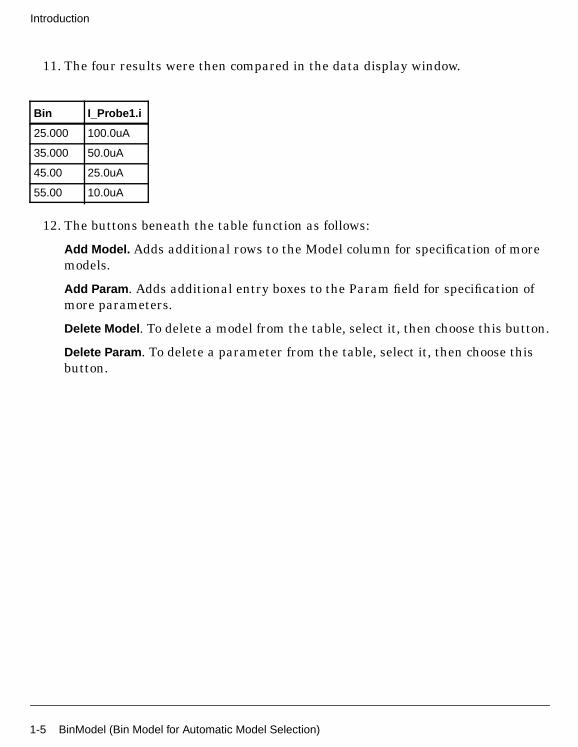
Bin I-Probe1.i
25.000 100.0uA
35.000 50.0uA
BinModel (Bin Model for Automatic Model Selection) 1-4
Introduction
11. The four results were then compared in the data display window.
12. The buttons beneath the table function as follows:
Add Model. Adds additional rows to the Model column for specification of moremodels.
Add Param . Adds additional entry boxes to the Param field for specification ofmore parameters.
Delete Model . To delete a model from the table, select it, then choose this button.
Delete Param . To delete a parameter from the table, select it, then choose thisbutton.
Bin I_Probe1.i
25.000 100.0uA
35.000 50.0uA
45.00 25.0uA
55.00 10.0uA
1-5 BinModel (Bin Model for Automatic Model Selection)

DataAccessComponent (Data Access Component)
Symbol
Parameters
File = filename
Type = file type
Block = block name
InterpMode = interpolation mode:
Index Lookup Specifies that iVal1, iVal2, etc. (described below) representthe integer indices (beginning with 0) of the independentvariables in the data file. Real iVal values are truncated first,for index lookup.
Value Lookup For real/integer independent variable, accesses the point inthe data file closest to the specified value. If midway, theaverage of the bracketing points is used.
Ceiling ValueLookup
For a real independent variable, accesses the nearest point inthe data file not less than the specified value.
Floor ValueLookup
For a real independent variable, accesses the nearest point inthe data file not greater than the specified value.
Linear, Cubic,Cubic Spline
Specifies the interpolation mode in each dimension, except forsplines, where only the innermost variable isspline-interpolated.
Value This is provided if the interpolation mode is variable orunknown, for example, as a passed parameter of asubnetwork. The resulting value should be a string (orinteger) from the following set: {“linear”(0), “spline”(1),“cubic”(2), “index_lookup”(3), “value_lookup”(4),“ceiling_value_lookup”(5), “floor_value_lookup”(6)}.
DataAccessComponent (Data Access Component) 1-6

Introduction
InterpDom = interpolation domain:
iVar1 = independent variable name or cardinality
iVal1 = independent variable value or index
iVar2 ... iVar10 = independent variable name or cardinality
iVal2 ... iVal10 = independent variable value or index
Notes/Equations/References
1. This component can be used to extract/interpolate multidimensional dependentvariables as a function of up to 10 independent variables. By setting the DACFile parameter to the desired filename, and setting the parameter of thecomponent of interest to point to the DAC (by Instance ID), the data in thespecified file can be accessed. (See “Example 1” on page 1-9)
You can quickly set all parameters (with matching names) of a device model bysetting the model’s AllParams parameter to the DAC’s Instance ID, which inturn, references the data file. Parameter names in a data file that are not devicemodel parameters are ignored. A device model parameter value that isexplicitly specified will override the value set by an AllParams association. (See“Example 2” on page 1-10)
You can also sweep over several BJT models using two DAC components. (See“Example 3” on page 1-11)
2. For a complex dependent variable, the two parts (real/imag, mag/degree, ordB/degree) are interpolated separately. For arc-like data (for exampleS-parameters vs. frequency), it may be more appropriate to interpolate in themag/degree domain.
3. This component is actually a special subnetwork whose expressions can be usedoutside. In particular, one of these expressions is _TREE (the multi-dimensionaltable). The following example shows using this expression with theget_max_points function.
Example: get_max_points(DAC1._TREE, "freq")
Rectangular Interpolates real and imaginary parts separately.Recommended for immitances.
Polar (arcinterpolation)
Interpolates magnitude and angle separately.Recommended for S-parameters.
DB Interpolates in dB and angle format.
1-7 DataAccessComponent (Data Access Component)

where:
DAC1._TREE represents the Instance ID of the DAC
"freq" represents the name of the independent variable
It returns the maximum # of points (over all sweeps of that variable) of theindependent variable (for discrete files with implicit row #, use 1 for the secondargument)
4. The Type parameter specifies the format of the disk file, which includesTouchstone, CITIfile, several MDIF types, SPW and binary datasets (possiblyfrom a previous simulation or via instrument server). For information on datafile formats, refer to Chapter 20 in the Circuit Simulation manual. The filesdisplayed in the Browser represent all files found based on the search pathsspecified by the DATA_FILES configuration variable.
5. The Block name specifies which table to use when the file contains two or moremultidimensional tables, e.g. ''ACDATA'', ''NDATA'' in an MDIF file, ''HB1.HB'',''HB1.HB_NOISE'' in a harmonic balance analysis dataset. A unique prefix issufficient; it can also be the sequence number (starting with 1) of the table, forexample, 1 for an ''ACDATA'' table and 2 for ''NDATA''. Note that the at symbol(@) should be used to suppress quotes when using a variable to identify a tableas the independent variable for making DAC parameter assignments.
6. Each iVar is either the name of an independent variable in the file (for example,Vgs) or is an integer representing the cardinality or nesting order of theindependent variable (1 being innermost). A cardinal value must be used whenan independent variable is implicit; for example, row index in discrete files isthe innermost independent variable. Note that the at symbol (@) must be usedto suppress quotes when using a variable, for example, @freq1, where freq1 is avariable declared in a VAR item.
Note that a string iVar parameter is searched in a case-preferential manner, i.e.,it is searched in a case-sensitive manner, failing that, it is searched again in acase-insensitive manner.
VARVAR1nRows=get_max_points(DAC1._TREE, 1)dindex=1
DCDC1SweepVar=''dindex''Start=1Stop=nRows
DataAccessComponent (Data Access Component) 1-8

Introduction
7. Each iVal is normally a real or integer value of the independent variable tobracket or search for in the file. If InterpMode is Index Lookup (which must bethe case for implicit variables), this value is the integer index, starting from 0.For example, the row value for a discrete file block runs from 0 to #rows − 1.
8. For all value lookup modes, a tolerance of 0.01% is used. A warning message isissued when extrapolation occurs.
Example 1
In this example, the resistance of resistor R1 is stepped through all of the valuesunder the “R” column in the file, “r.mdf”.
The contents of the r.mdf file:
% INDEX R Rsh Length Width
1 100 1.0 2.0 3.02 101 4 5 63 51 9 8 74 10 123 22 11END
RR1R=file{DAC1, ''R''}
DataAccessComponentDAC1File=”r.mdf”Type=DiscreteInterpMode=Index LookupiVar1=1iVal1=dindex-1
DCDC1SweepVar=''dindex''
1-9 DataAccessComponent (Data Access Component)

Example 2
In this example, the resistor model RM1 accesses the parameters R, Rsh, Length andWidth from the discrete file r.mdf.
RR1Model=RM1
DataAccessComponentDAC1File=”r.mdf”iVar1=1iVal1=dindex-1
R_ModelRM1AllParams=DAC1
The contents of the r.mdf file:
% INDEX R Rsh Length Width
1 100 1.0 2.0 3.02 101 4 5 63 51 9 8 74 10 123 22 11END
DataAccessComponent (Data Access Component) 1-10

Introduction
Example 3
This example shows how a pair of DACs can be used to sweep over several BJTmodels. The first DAC, STEER, retrieves a model filename from a discrete filebfqtm.txt, and the second DAC, DAC_BJT, retrieves the model data.
Note An assignment of the type: R1=file{DAC1, ''Rnom''}, is equivalent to theexpression R1=dep_data(DAC1._DAC, “Rnom” ).
DataAccessComponentSTEERFile=''bfqtm.txt''Type=DiscreteiVar1=1iVal1=INDEX-1
DataAccessComponentDAC_BJTFile=file{STEER, ''filename''}Type=MDIF model
BJT_NPNBJT3Model=BJTM1
EE_BJT2_ModelBJTM1AllParams=DAC_BJT
Contents of the file''bfqtm.txt''. Each of these.txt files has a different setof EE_BJT2_Modelparameters.
1-11 DataAccessComponent (Data Access Component)

FORMAT A, B, C, D, E (Drawing Formats)
Drawing
Parameters
None
Notes/Equations/References
1. The Drawing Formats library provides popular sheet sizes (in inches):A (8.5×11), B (11×17), C (17×22), D (22×34), E (34×44).
2. Turn on Drawing Format filter through Options > Preferences > Select. You canthen move or delete the drawing sheet. Turn off the filter when not needed.
FORMAT A, B, C, D, E (Drawing Formats) 1-12

Introduction
Ground (Ground Component)
Symbol
Parameters
None
Notes/Equations/References
1. When you place a ground, position the pin directly on the end of the pin or wireto which you are connecting.
1-13 Ground (Ground Component)

Introduction
Port (Port Component)
Symbol
Parameters
Num = port number (value type integer)
layer = (for Layout option) layer to which port is mapped
Range of Usage
Unlimited
Notes/Equations/References
1. Port is the standard port component offered and used to define networks.
2. When you place a port, position the square directly on the end of the pin or wireto which you are connecting.
3. The number of ports of a network is the same as the number of Port componentsconnected in it.
4. The port number is supplied by the program and automatically incrementedeach time a Port is placed. However, you can override the program-suppliedvalue by typing in an integer value of your choice. Port numbers must beconsecutive; and, port numbers of multiple Port components cannot be thesame.
1-14
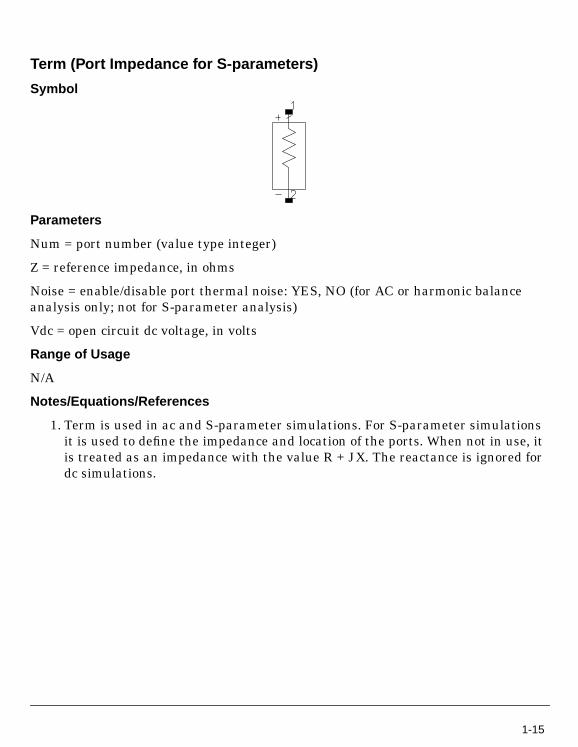
Term (Port Impedance for S-parameters)
Symbol
Parameters
Num = port number (value type integer)
Z = reference impedance, in ohms
Noise = enable/disable port thermal noise: YES, NO (for AC or harmonic balanceanalysis only; not for S-parameter analysis)
Vdc = open circuit dc voltage, in volts
Range of Usage
N/A
Notes/Equations/References
1. Term is used in ac and S-parameter simulations. For S-parameter simulationsit is used to define the impedance and location of the ports. When not in use, itis treated as an impedance with the value R + JX. The reactance is ignored fordc simulations.
1-15
Introduction
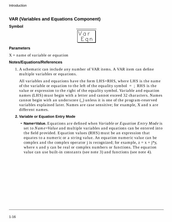
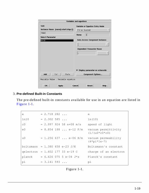
VAR (Variables and Equations Component)
Symbol
Parameters
X = name of variable or equation
Notes/Equations/References
1. A schematic can include any number of VAR items. A VAR item can definemultiple variables or equations.
All variables and equations have the form LHS=RHS, where LHS is the nameof the variable or equation to the left of the equality symbol = ; RHS is thevalue or expression to the right of the equality symbol. Variable and equationnames (LHS) must begin with a letter and cannot exceed 32 characters. Namescannot begin with an underscore (_) unless it is one of the program-reservedvariables explained later. Names are case sensitive; for example, X and x aredifferent names.
2. Variable or Equation Entry Mode
• Name=Value. Equations are defined when Variable or Equation Entry Mode isset to Name=Value and multiple variables and equations can be entered intothe field provided. Equation values (RHS) must be an expression thatequates to a numeric or a string value. An equation numeric value can becomplex and the complex operator j is recognized; for example, z = x + j*y,where x and y can be real or complex numbers or functions. The equationvalue can use built-in constants (see note 3) and functions (see note 4).
1-16

• Standard. Variables are defined when the Variable or Equation Entry Mode isset to Standard, a single variable can be entered into the fields provided.Variable Value must be a numeric value (2.567, for example) or a string valueenclosed in double-quote symbols. For example, the string value for aprecision type of parameter can be defined as 2.14 for Signal Processing, or“MSUB1” for Circuit. Variable values can also be defined as a nominal valuewith associated optimization range.
Note that expression X has anumeric value; expression Y uses apredefined constant; expression Zuses a predefined function.
1-17
Introduction
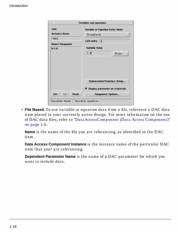
• File Based. To use variable or equation data from a file, reference a DAC dataitem placed in your currently active design. For more information on the useof DAC data files, refer to “DataAccessComponent (Data Access Component)”on page 1-6.
Name is the name of the file you are referencing, as identified in the DACitem.
Data Access Component Instance is the instance name of the particular DACitem that your are referencing.
Dependent Parameter Name is the name of a DAC parameter for which youwant to include data.
1-18
3. Pre-defined Built-in Constants
The pre-defined built-in constants available for use in an equation are listed inFigure 1-1.
Figure 1-1.
e = 2.718 282 ... e
ln10 = 2.302 585 ... ln(10)
c0 = 2.997 924 58 e+08 m/s speed of light
e0 = 8.854 188 ... e-12 F/m vacuum permittivity(1/(u0*c0*c0)
u0 = 1.256 637 ... e-06 H/m vacuum permeability(4*pi*1e-7)
boltzmann = 1.380 658 e-23 J/K Boltzmann's constant
qelectron = 1.602 177 33 e-19 C charge of an electron
planck = 6.626 075 5 e-34 J*s Planck's constant
pi = 3.141 593 ... pi
1-19

Introduction
4. Pre-defined Built-in Functions
Function arguments have the following meaning.
• x, y are complex
• r, r0, r1, rx, ry, lower_bound, upper_bound are real
• s, s1, s2 are strings
In general, the functions return a complex number, unless it is a string operatoras noted (refer to Figure 1-2.) A function that returns a real value effectivelyhas a zero value imaginary term.
1-20
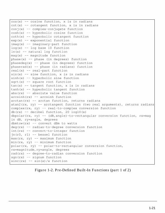
Figure 1-2. Pre-Defined Built-In Functions (part 1 of 2)
cos(x) -- cosine function, x is in radianscot(x) -- cotangent function, x is in radiansconj(x) -- complex-conjugate functioncosh(x) -- hyperbolic cosine functioncoth(x) -- hyperbolic cotangent functionexp(x) -- exponential functionimag(x) -- imaginary-part functionlog(x) -- log base 10 functionln(x) -- natural log functionmag(x) -- magnitude functionphase(x) -- phase (in degrees) functionphasedeg(x) -- phase (in degrees) functionphaserad(x) -- phase (in radians) functionreal(x) -- real-part functionsin(x) -- sine function, x is in radianssinh(x) -- hyperbolic sine functionsqrt(x) -- square root functiontan(x) -- tangent function, x is in radianstanh(x) -- hyperbolic tangent functionabs(rx) -- absolute value functionarcsinh(rx) -- arcsinh functionarctan(rx) -- arctan function, returns radiansatan2(rx, ry) -- arctangent function (two real arguments), returns radianscomplex(rx, ry) -- real-to-complex conversion functiondb(rx) -- decibel function, 20 log10(x)dbpolar(rx, ry) -- (dB,angle)-to-rectangular conversion function, rx=magin dB, ry=angle, degreesdbmtow(rx) -- convert dBm to wattsdeg(rx) -- radian-to-degree conversion functionint(rx) -- convert-to-integer functionjn(r0, r1) -- bessel functionmax(rx, ry) -- maximum functionmin(rx, ry) -- minimum functionpolar(rx, ry) -- polar-to-rectangular conversion function,rx=magnitude,ry=angle, degreesrad(rx) -- degree-to-radian conversion functionsgn(rx) -- signum functionsinc(rx) -- sin(x)/x function
1-21

Introduction
5. Equation Editor Syntax
Mathematical expressions entered equations can include the following items.
• Blank spaces Blank spaces within an expression are ignored; they can beused to improve readability. For example,4 * (x + .1) evaluates the same as4*(x+.1)
• Numerical constants Real numbers such as 12.68, exponential notationnumbers such as 1e6 or 25.1e3, pi can be used, and complex numbers can bedefined. For example, z = x + j*y.
• LHS form assignment The LHS assignment takes the form of integer,double, complex or string dependent on what form is associated with theRHS. For example,
sprintf(...) -- formatted print utility; returns a string
strcat(...) -- string concatenation utility; returns a string
example: x = 2
y = 14
z = sprintf( "%i.%i", x, y)
results in the string "2.14"
sprintf follows standard C programming syntax
This sprintf() function may only have three arguments as shown.The first argument being the composite string format. thesecond and third arguments must be either a format. the secondand third arguments must be either a integer, double, or stringvalue. The format string for an integer is %i, for a double is%d, and for a string is %s.
example: s1 = "my cat"
s2 = " is frisky"
s3 = strcat( s1, s2)
results in the string "my cat is frisky"
This strcat() function may only have the two arguments shown.Each argument must be a string. An explicit string may besubstituted for each argument such as: s3 = strcat( “my cat”, “is frisky”)
Figure 1-2. Pre-Defined Built-In Functions (part 2 of 2)
1-22

X=4, Y=4.0, W=1.0+j*3.0, Z=" 4"
associates the form of integer, double, complex and string to X, Y, W and Z,respectively. The LHS form is important when subsequently used infollowing expressions.
• Mathematical operators Standard operators are available:
** exponentiation^exponentiation* multiplication/ division+ addition− subtraction
In evaluating an expression, operator precedence is: ** ^ * / + − .Operators at the same level (for example * / ) are evaluated left to right.Any number of parentheses pairs can be used to modify an expression in theusual way. For example
C10 * (1 + .005) evaluates differently thanC10 *1 + .005
• Parameters of a parametric subnetwork Any formal parameters that arepassed into a parametric subnetwork can be included in equations defined inthat subnetwork. These parameters are defined for a schematic design usingthe File > Design/Parameters menu selection.
• Use of if...then...else...endif statements An equation can use a conditionalstatement: if ( conditional expression) then ( expression1) else(expression2) endif. For example,
X = 1Y = if ( X>0) then ( cos( pi/8) ) else ( sin( pi/8) ) endif
The conditional expression can be a simple or complex numeric conditionalexpression with arguments separated by the standard symbols:
< > <= >= = != &&
Each expression can be any valid numeric expression. The entireif...then...else...endif expression must be on one line.
1-23

Introduction
MultiplicityThe aim of the multiplicity feature is provide a convenient method to scalecomponents or entire sub-circuits containing many components and sub-circuits.Given a component with some value M of Multiplicity, the simulator treats thiscomponent as if there were M such components all connected in parallel. Sub-circuitsincluding within sub-circuits will be appropriately scaled. M does not have to be aninteger.
The parameter is available from the component level as an additional parameter(_M) for several components and devices. For example, in the Gummel-Poon BJT, it isadded at the instance level, as shown here. Note that the default visibility setting isoff for this parameter.
1-24 Multiplicity
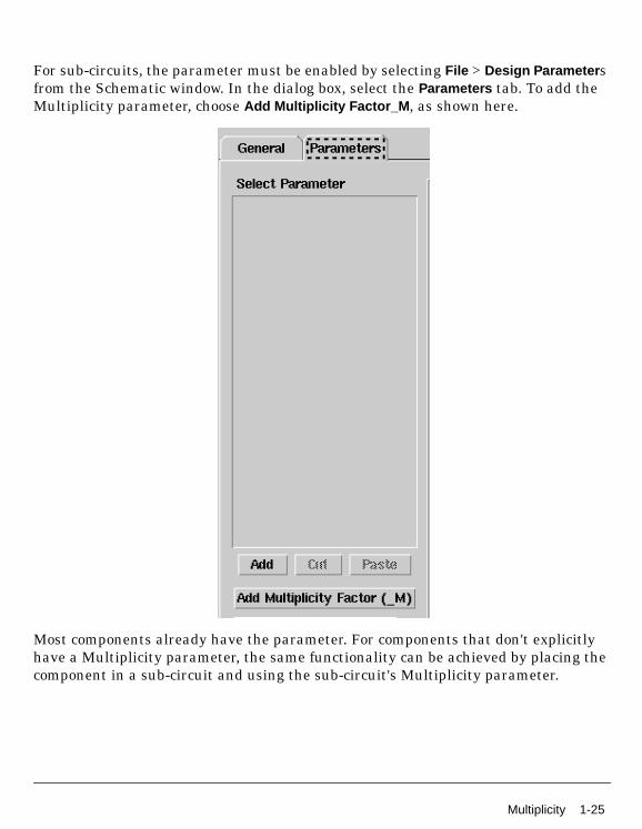
For sub-circuits, the parameter must be enabled by selecting File > Design Parameter sfrom the Schematic window. In the dialog box, select the Parameters tab. To add theMultiplicity parameter, choose Add Multiplicity Factor_M , as shown here.
Most components already have the parameter. For components that don't explicitlyhave a Multiplicity parameter, the same functionality can be achieved by placing thecomponent in a sub-circuit and using the sub-circuit's Multiplicity parameter.
Multiplicity 1-25

Introduction
Components from Product MigrationThe following lists of components include those from older products, such as Series IVor MDS that can still be placed in ADS designs. There is no documentation currentlyavailable for these components, but they are identified here for your convenience.
None of these are accessible from the component library browser or palettes, but canbe placed in the Schematic window by typing the exact name (as shown) into theComponent History box above the drawing area, then pressing Enter and movingyour cursor to the drawing area.
Component Categories
The following categories of components are included:
• Series IV Components
• Spectral Sources
• Wideband Modems
• Other MDS Components
Series IV Components
• GAIN
• PULSE_TRAIN
Spectral Sources
• GMSK_SOURCE
• PIQPSK_SOURCE
• QAM16_SOURCE
• QPSK_SOURCE
Wideband Modems
• AM_DemodBroad
• AM_ModBroad
• FM_DemodBroad
1-26 Components from Product Migration
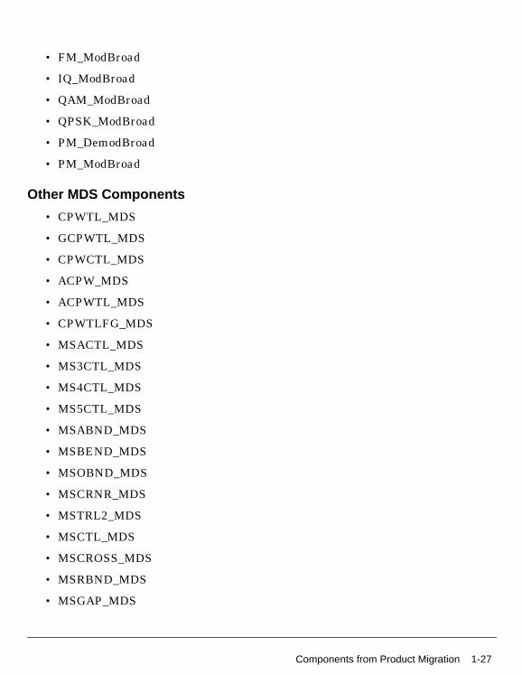
• FM_ModBroad
• IQ_ModBroad
• QAM_ModBroad
• QPSK_ModBroad
• PM_DemodBroad
• PM_ModBroad
Other MDS Components
• CPWTL_MDS
• GCPWTL_MDS
• CPWCTL_MDS
• ACPW_MDS
• ACPWTL_MDS
• CPWTLFG_MDS
• MSACTL_MDS
• MS3CTL_MDS
• MS4CTL_MDS
• MS5CTL_MDS
• MSABND_MDS
• MSBEND_MDS
• MSOBND_MDS
• MSCRNR_MDS
• MSTRL2_MDS
• MSCTL_MDS
• MSCROSS_MDS
• MSRBND_MDS
• MSGAP_MDS
Components from Product Migration 1-27

Introduction
• MSAGAP_MDS
• MSIDCF_MDS
• MSIDC_MDS
• MSLANGE_MDS
• MSTL_MDS
• MSOC_MDS
• MSSPLC_MDS
• MSSPLS_MDS
• MSSPLR_MDS
• MSSTEP_MDS
• MSRTL_MDS
• MSSLIT_MDS
• MSTAPER_MDS
• MSTEE_MDS
• TFC_MDS
• MSWRAP_MDS
• TFR_MDS
• MSVIA_MDS
• MSSVIA_MDS
• MLACRNR1
• MLCRNR1
• MLRADIAL1
• MLSLANTED1
• MLCROSSOVER1
• SLTL_MDS
• SLOC_MDS
• SLCTL_MDS
1-28 Components from Product Migration

• SL3CTL_MDS
• SL4CTL_MDS
• SL5CTL_MDS
• SLUCTL_MDS
• SLGAP_MDS
• SLSTEP_MDS
• SLTEE_MDS
• SLOBND_MDS
• SLCNR_MDS
• SLRBND_MDS
• SLABND_MDS
• SLUTL_MDS
• SSTL_MDS
• SSCTL_MDS
• SS3CTL_MDS
• SS4CTL_MDS
• SS5CTL_MDS
• SSSPLC_MDS
• SSPLS_MDS
• SSPLR_MDS
• SSLANGE_MDS
• SSTFR_MDS
• BRCTL_MDS
• BR0CTL_MDS
• BR3CTL_MDS
• BR4CTL_MDS
• CTL_MDS
Components from Product Migration 1-29
Introduction
• COAX_MDS
• DRC_MDS
• TL_MDS
• TLOC_MDS
• RWGTL_MDS
• FINLINE_MDS
• ETAPER_MDS
• SLOTTL_MDS
• RIBBONG_MDS
• RIBBONS_MDS
• WIREG_MDS
• WIRES_MDS
1-30 Components from Product Migration

Chapter 2: Lumped Components
2-1

Lumped Components
C (Capacitor)
Symbol
Parameters
C = capacitance, in farads
Temp = temperature, in °C
Tnom = nominal temperature, in °C
TC1 = linear temperature coefficient, in 1/°C
TC2 = quadratic temperature coefficient, in 1/°C2
wBV = breakdown voltage warning, in volts
InitCond = initial condition voltages for transient analysis, in volts; when specified,the check-box “Use user-specified initial conditions” in the Convergence tab of theSimulation-Transient control item must be enabled for this condition to take effect.
Model = name of a capacitor model to use
Width = physical width for use with a model
Length = physical length for use with a model
_M = number of capacitors in parallel (default: 1)
Range of Usage
N/A
Notes/Equations/References
1. The capacitor value can be made a function of temperature by setting Tnom andeither TC1 or TC2 or both. Tnom specifies the nominal temperature at which Cis given. Tnom defaults to 25°C. If Temp≠Tnom, then the simulated capicatancevalue is given by:
C′ = C × [1 + TC1 (Temp − Tnom) + TC2 (Temp − Tnom)2]
2. If Temp is not explicitly specified, it defaults to the global temperature specifiedin the options item.
2-2 C (Capacitor)

3. wBV is used by the overload alert feature. It sets a limit on the maximumvoltage across the capacitor. If this limit is specified, the simulator will issue awarning the first time it is exceeded during a dc, harmonic balance or transientsimulation. Simulation results are not affected by this parameter.
4. If a model name is given, then values that are not specified on the capacitorinstance are taken from the model values. Typical values that can be defaultedare capacitance, length and width, nominal temperature, temperaturecoefficients, and overload alert parameters.
If a model is used, the capacitance value to be simulated (before temperaturescaling is applied) is computed as:
C′ = C + Cj × (Length −2 × Narrow) × (Width −2 × Narrow)
+ Cjsw × 2 × (Length + Width −4 × Narrow)
5. _M is used to represent the number of capacitors in parallel and defaults to 1. Ifa capacitor model is used, an optional scaling parameter Scale can also bedefined on the model; it defaults to 1. The effective capacitance that will besimulated is C*Scale*M.
6. When InitCond is explicitly specified, the check-box Use user-specified initialconditions must be turned on in the Convergence tab of theSimulation-Transient controller for the parameter setting to take effect.
C (Capacitor) 2-3

Lumped Components
C_Model (Capacitor Model)
Symbol
Parameters
C = default fixed capacitance, in farads (default: 1 pF)
Cj = junction capacitance, in farads/meter2
Cjsw = sidewall or periphery capacitance, in farads/meter
Length = default length, in specified units
Width = default width, in specified units
Narrow = length and width narrowing due to etching, in specified units
Tnom = nominal temperature, in °C
TC1 = linear temperature coefficient, in 1/°C
TC2 = quadratic temperature coefficient, in 1/°C2
wBV = breakdown voltage (warning), in volts
AllParams = DataAccessComponent-based parameters
Scale = capacitance scaling factor (default:1)
Range of Usage
N/A
Notes/Equations/References
1. This model supplies values for a capacitor C. This allows physically-basedcapacitors to be modeled based on length and width.
2. Use AllParams with a DataAccessComponent to specify file-based parameters(refer to DataAccessComponent). Note that model parameters that areexplicitly specified take precedence over those specified via AllParams.
2-4 C_Model (Capacitor Model)

C_Conn (Capacitor (Connector Artwork))
Symbol
Parameters
C = capacitance, in farads
Range of Usage
N/A
Notes/Equations/References
1. This component is a single connection in layout. For example, it can be used torepresent parasitics.
C_Conn (Capacitor (Connector Artwork)) 2-5

Lumped Components
C_Pad1 (Capacitor (Pad Artwork))
Symbol
Parameters
C = capacitance, in farads
W = width of pad, in specified units
S = spacing, in specified units
L1 = (for Layout option) pin-to-pin distance, in specified units
Range of Usage
N/A
Notes/Equations/References
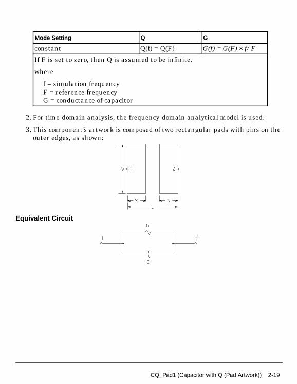
1. This component’s artwork is composed of two rectangular pads with pins on theouter edges, as shown:
2-6 C_Pad1 (Capacitor (Pad Artwork))

C_Space (Capacitor (Space Artwork))
Symbol
Parameters
C = capacitance, in farads
L1 = (for Layout option) pin-to-pin distance, in specified units
Range of Usage
N/A
Notes/Equations/References
1. This component is represented as a connected gap in layout—into which acustom artwork object can be inserted.
C_Space (Capacitor (Space Artwork)) 2-7

Lumped Components
CAPP2_Conn (Chip Capacitor (Connector Artwork))
Symbol
Parameters
C = capacitance, in farads
TanD = dielectric loss tangent
Q = quality factor
FreQ = resistance frequency for Q, in hertz
FreqRes = resistance frequency, in hertz
Exp = exponent for frequency dependence of Q
Range of Usage
C, Q, FreqQ, FreqRes ≥ 0
Notes/Equations/References
1. The series resistance Rs is determined by the Q and the parallel resistance Rp isdetermined by TanD.
The frequency-dependence of Q is given by
Q (f) = Q (FQ) × (FreqQ/f)Exp
where f is the simulation frequency and Q(FreqQ) is the specified value of Q atFreqQ.
2. If Q or FreqQ are set to 0, Q is assumed to be infinite.
3. For time-domain analysis, the frequency-domain analytical model is used.
4. This component has no default artwork associated with it.
5. Cris Bowick, RF Circuit Design, Howard Sams & Co., 1987.
6. The RF Capacitor Handbook, American Technical Ceramics Corp., September1983.
2-8 CAPP2_Conn (Chip Capacitor (Connector Artwork))
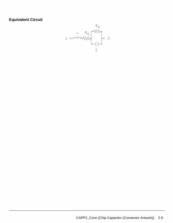
Equivalent Circuit
CAPP2_Conn (Chip Capacitor (Connector Artwork)) 2-9

Lumped Components
CAPP2_Pad1 (Chip Capacitor (Pad Artwork))
Symbol
Parameters
C = capacitance, in farads
TanD = dielectric loss tangent
Q = quality factor
FreQ = resistance frequency for Q, in hertz
FreqRes = resistance frequency, in hertz
Exp = exponent for frequency dependence of Q
W = (for Layout option) width of pad, in specified units
S = (for Layout option) spacing, in specified units
L1 = (for Layout option) pin-to-pin distance, in specified units
Range of Usage
C, Q, FreqQ, FreqRes ≥ 0
Notes/Equations/References
1. The series resistance Rs is determined by the Q and the parallel resistance Rp isdetermined by TanD.
The frequency-dependence of Q is given by
Q (f) = Q (FreqQ) × (FreqQ/f)Exp
where f is the simulation frequency and Q(FreqQ) is the specified value of Q atFreqQ.
2. If Q or FreqQ are set to 0, Q is assumed to be infinite.
3. For time-domain analysis, the frequency-domain analytical model is used.
2-10 CAPP2_Pad1 (Chip Capacitor (Pad Artwork))

4. This component’s artwork is composed of two rectangular pads with pins on theouter edges.
5. Bowick, Cris. RF Circuit Design, Howard Sams & Co., 1987.
6. The RF Capacitor Handbook, American Technical Ceramics Corp., September1983.
Equivalent Circuit
CAPP2_Pad1 (Chip Capacitor (Pad Artwork)) 2-11

Lumped Components
CAPP2_Space (Chip Capacitor (Space Artwork))
Symbol
Parameters
C = capacitance, in farads
TanD = dielectric loss tangent
Q = quality factor
FreQ = resistance frequency for Q, in hertz
FreqRes = resistance frequency, in hertz
Exp = exponent for frequency dependence of Q
L1 = (for Layout option) pin-to-pin distance, in specified units
Range of Usage
C, Q, FreqQ, FR ≥ 0
Notes/Equations/References
1. The series resistance Rs is determined by the Q and the parallel resistance Rp isdetermined by TanD.
The frequency-dependence of Q is given by
Q (f) = Q (FreqQ) × (FreqQ/f)Exp
where f is the simulation frequency and Q(FreqQ) is the specified value of Q atFreqQ.
2. If Q or FreqQ are set to 0, Q is assumed to be infinite.
3. For time-domain analysis, the frequency-domain analytical model is used.
4. This component is represented as a connected gap in layout—into which acustom artwork object can be inserted.
5. Bowick, Cris. RF Circuit Design, Howard Sams & Co., 1987.
6. The RF Capacitor Handbook, American Technical Ceramics Corp., September1983.
2-12 CAPP2_Space (Chip Capacitor (Space Artwork))

Equivalent Circuit
CAPP2_Space (Chip Capacitor (Space Artwork)) 2-13
Lumped Components
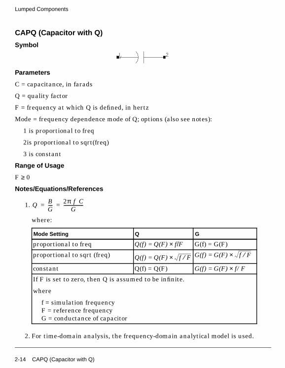
CAPQ (Capacitor with Q)
Symbol
Parameters
C = capacitance, in farads
Q = quality factor
F = frequency at which Q is defined, in hertz
Mode = frequency dependence mode of Q; options (also see notes):
1 is proportional to freq
2is proportional to sqrt(freq)
3 is constant
Range of Usage
F ≥ 0
Notes/Equations/References
1. /
where:
2. For time-domain analysis, the frequency-domain analytical model is used.
Mode Setting Q G
proportional to freq Q(f) = Q(F) × f/F G(f) = G(F)
proportional to sqrt (freq) Q(f) = Q(F) × G(f) = G(F) ×
constant Q(f) = Q(F) G(f) = G(F) × f/F
If F is set to zero, then Q is assumed to be infinite.
where
f = simulation frequencyF = reference frequencyG = conductance of capacitor
Q BG---- 2π f C
G------------------= =
f F⁄ f F⁄
2-14 CAPQ (Capacitor with Q)
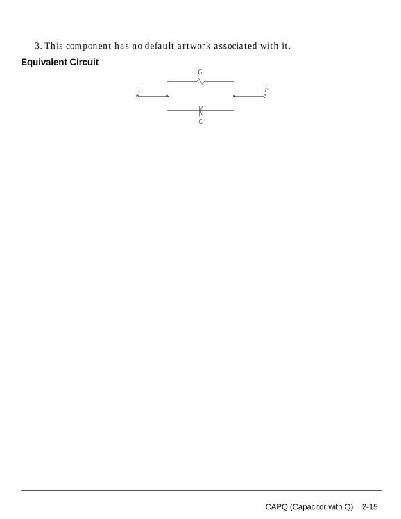
3. This component has no default artwork associated with it.
Equivalent Circuit
CAPQ (Capacitor with Q) 2-15

Lumped Components
CQ_Conn (Capacitor with Q (Connector Artwork))
Symbol
Parameters
C = capacitance, in farads
Q = quality factor
F = frequency at which Q is defined, in hertz
Mode = frequency dependence mode of Q; options (also see notes):
1 is proportional to freq
2 is proportional to sqrt(freq)
3 is constant
Range of Usage
F ≥ 0
Notes/Equations/References
1.
where:
2. For time-domain analysis, the frequency-domain analytical model is used.
Mode Setting Q G
proportional to freq Q(f) = Q(F) × f/F G(f) = G(F)
proportional to sqrt (freq) Q(f) = Q(F) × G(f) = G(F) ×
constant Q(f) = Q(F) G(f) = G(F) × f/F
If F is set to zero, then Q is assumed to be infinite.
where
f = simulation frequencyF = reference frequencyG = conductance of capacitor
Q BG---- 2π f C
G------------------= =
f F⁄ f F⁄
2-16 CQ_Conn (Capacitor with Q (Connector Artwork))

3. This component is a single connection in layout. For example, it can be used torepresent parasitics.
Equivalent Circuit
CQ_Conn (Capacitor with Q (Connector Artwork)) 2-17

Lumped Components
CQ_Pad1 (Capacitor with Q (Pad Artwork))
Symbol
Parameters
C = capacitance, in farads
Q = quality factor
F = frequency at which Q is defined, in hertz
Mode = frequency dependence mode of Q; options (also see notes):
1 is proportional to freq
2 is proportional to sqrt(freq)
3 is constant
W = (for Layout option) width of pad, in specified units
S = (for Layout option) spacing, in specified units
L1 = (for Layout option) pin-to-pin distance, in specified units
Range of Usage
F ≥ 0
Notes/Equations/References
1.
where:
Mode Setting Q G
proportional to freq Q(f) = Q(F) × f/F G(f) = G(F)
proportional to sqrt (freq) Q(f) = Q(F) × G(f) = G(F) ×
Q BG---- 2π f C
G------------------= =
f F⁄ f F⁄
2-18 CQ_Pad1 (Capacitor with Q (Pad Artwork))
2. For time-domain analysis, the frequency-domain analytical model is used.
3. This component’s artwork is composed of two rectangular pads with pins on theouter edges, as shown:
Equivalent Circuit
constant Q(f) = Q(F) G(f) = G(F) × f/F
If F is set to zero, then Q is assumed to be infinite.
where
f = simulation frequencyF = reference frequencyG = conductance of capacitor
Mode Setting Q G
CQ_Pad1 (Capacitor with Q (Pad Artwork)) 2-19

Lumped Components
CQ_Space (Capacitor with Q (Space Artwork))
Symbol
Parameters
C = capacitance, in farads
Q = quality factor
F = frequency at which Q is defined, in hertz
Mode = frequency dependence mode of Q; options (also see notes):
1 is proportional to freq
2 is proportional to sqrt(freq)
3 is constant
L1 = (for Layout option) pin-to-pin distance, in specified units
Range of Usage
F ≥ 0
Notes/Equations/References
1.
where:
Mode Setting Q G
proportional to freq Q(f) = Q(F) × f/F G(f) = G(F)
proportional to sqrt (freq) Q(f) = Q(F) × G(f) = G(F) ×
constant Q(f) = Q(F) G(f) = G(F) × f/F
If F is set to zero, then Q is assumed to be infinite.
where
f = simulation frequencyF = reference frequencyG = conductance of capacitor
Q BG---- 2π f C
G------------------= =
f F⁄ f F⁄
2-20 CQ_Space (Capacitor with Q (Space Artwork))

2. For time-domain analysis, the frequency-domain analytical model is used.
3. This component is represented as a connected gap in layout—into which acustom artwork object can be inserted.
Equivalent Circuit
CQ_Space (Capacitor with Q (Space Artwork)) 2-21
Lumped Components
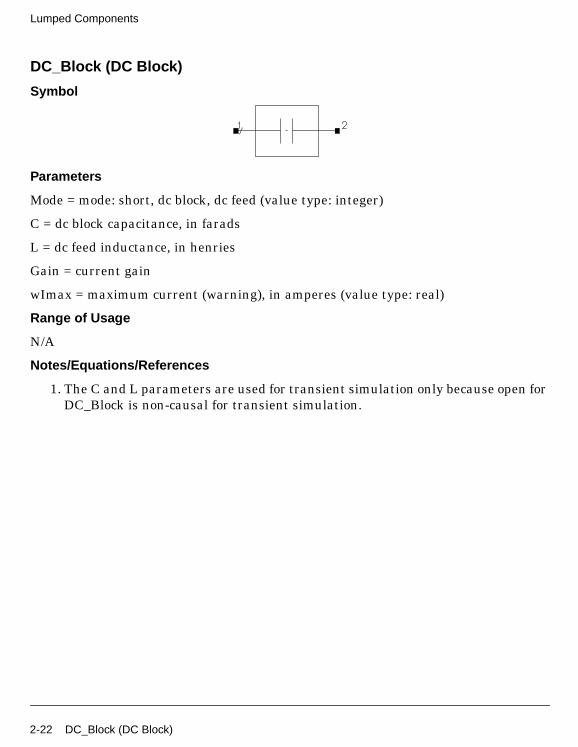
DC_Block (DC Block)
Symbol
Parameters
Mode = mode: short, dc block, dc feed (value type: integer)
C = dc block capacitance, in farads
L = dc feed inductance, in henries
Gain = current gain
wImax = maximum current (warning), in amperes (value type: real)
Range of Usage
N/A
Notes/Equations/References
1. The C and L parameters are used for transient simulation only because open forDC_Block is non-causal for transient simulation.
2-22 DC_Block (DC Block)
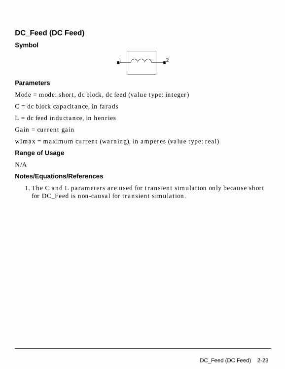
DC_Feed (DC Feed)
Symbol
Parameters
Mode = mode: short, dc block, dc feed (value type: integer)
C = dc block capacitance, in farads
L = dc feed inductance, in henries
Gain = current gain
wImax = maximum current (warning), in amperes (value type: real)
Range of Usage
N/A
Notes/Equations/References
1. The C and L parameters are used for transient simulation only because shortfor DC_Feed is non-causal for transient simulation.
DC_Feed (DC Feed) 2-23

Lumped Components
DICAP (Dielectric Laboratories Di-cap Capacitor)
Symbol
Illustration:
Parameters
W = width of metal plates and dielectric, in specified units
L = length of metal plates and dielectric, in specified units
T = thickness of dielectric, in specified units
Er = dielectric constant
TanDeL = dielectric loss tangent value at 1 MHz
RO = series resistance at 1 GHz, in ohms
Range of Usage
N/A
Notes/Equations/References
1. This is the Di-cap capacitor model by Dielectric Laboratories Incorporated; forthe parameter values, please contact Dielectric Laboratories.
2. DICAP is a single-layer capacitor that behaves as lossy parallel platetransmission lines. Pin 1 is on the bottom metal plate; pin 2 is on the top metalplate. The connection (such as Wire or Ribbon) from the top metal plate (pin 2)to the connecting transmission line is not included in the model—the user mustconnect it separately.
3. For time-domain analysis, the frequency-domain analytical model is used.
2-24 DICAP (Dielectric Laboratories Di-cap Capacitor)

4. In the layout, the top metal will be drawn on layer cond2; the bottom metal onlayer cond; and, the capacitor dielectric on layer diel.
DICAP (Dielectric Laboratories Di-cap Capacitor) 2-25
Lumped Components
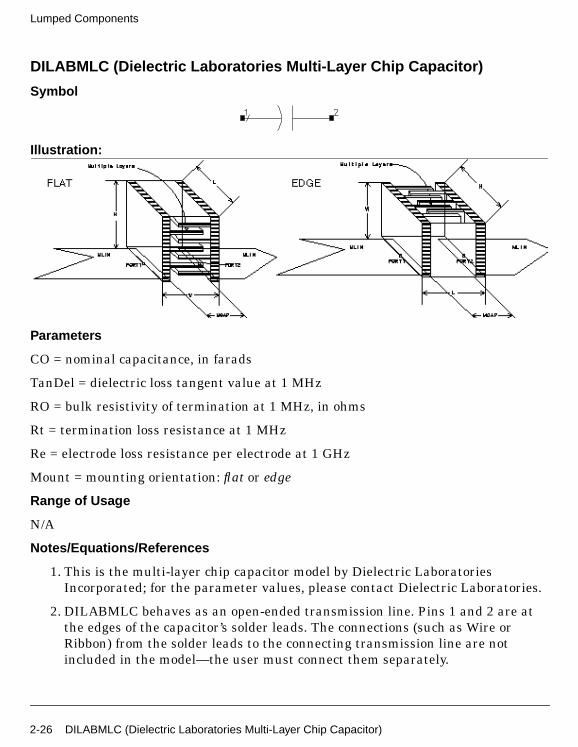
DILABMLC (Dielectric Laboratories Multi-Layer Chip Capacitor)
Symbol
Illustration:
Parameters
CO = nominal capacitance, in farads
TanDel = dielectric loss tangent value at 1 MHz
RO = bulk resistivity of termination at 1 MHz, in ohms
Rt = termination loss resistance at 1 MHz
Re = electrode loss resistance per electrode at 1 GHz
Mount = mounting orientation: flat or edge
Range of Usage
N/A
Notes/Equations/References
1. This is the multi-layer chip capacitor model by Dielectric LaboratoriesIncorporated; for the parameter values, please contact Dielectric Laboratories.
2. DILABMLC behaves as an open-ended transmission line. Pins 1 and 2 are atthe edges of the capacitor’s solder leads. The connections (such as Wire orRibbon) from the solder leads to the connecting transmission line are notincluded in the model—the user must connect them separately.
2-26 DILABMLC (Dielectric Laboratories Multi-Layer Chip Capacitor)
3. For transient analysis, the DILABMLC is modelled as a series RLC equivalentcircuit.
4. For convolution analysis, the frequency domain analytical model is used.
5. Attention should be given on the mounting orientation of the DILABMLCcapacitor (whether it is flat or edge-mounted). The orientation of the capacitorrelative to the gap in the microstrip affects the sequence of resonances.
When the internal electrodes are parallel to the plane of the microstrip (flatmounted) parallel resonances occur when the equivalent line length is either aneven or odd multiple of a half wave-length.
When the internal electrodes are normal to the substrate (edge mounted),resonances occur only when the multiple is even. This suppression ofodd-ordered resonances it the result of exciting the equivalent line at its centerrather than at one end. Consequently, resonance occurs at higher frequencieswhen edge mounted.
DILABMLC (Dielectric Laboratories Multi-Layer Chip Capacitor) 2-27

Lumped Components
INDQ (Inductor with Q)
Symbol
Parameters
L = inductance, in henries
Q = quality factor
F = frequency at which Q is given, in hertz
Mode = loss mode for this device; options (also see notes):
1 is proportional to freq
2 is proportional to sqrt(freq)
3 is constant
Rdc = resistance for modes 2 and 3
Range of Usage
F ≥ 0
Notes/Equations/References
1.
where:
Mode Setting Q R
proportional to freq Q(f) = Q(F) × f/F R(f) = R(F)
proportional to sqrt (freq) Q(f) = Q(F) × R(f) = R(F) ×
constant Q(f) = Q(F) R(f) = R(F) × f/F
If F is set to zero, then Q is assumed to be infinite.
where
f = simulation frequencyF = reference frequencyR = resistance of inductor
Q 2πfLR
-------------=
f F⁄ f F⁄
2-28 INDQ (Inductor with Q)

2. For time-domain analysis, the frequency-domain analytical model is used.
3. This component has no default artwork associated with it.
Equivalent Circuit
INDQ (Inductor with Q) 2-29

Lumped Components
L (Inductor)
Symbol
Parameters
L = inductance, in henries
R = series resistance, in ohms
Temp = temperature, in °C
Tnom = nominal temperature, in °C
TC1 = linear temperature coefficient, in 1/°C
TC2 = quadratic temperature coefficient, in 1/°C2
InitCond = transient analysis initial condition current, in amperes; when specified,the check-box “Use user-specified initial conditions” in the Convergence tab of theSimulation-Transient control item must be enabled for this condition to take effect.
_M = number of inductors in parallel (default: 1)
Range of Usage
N/A
Notes/Equations/References
1. The inductor value can be made a function of temperature by setting Tnom andeither TC1 or TC2 or both. Tnom specifies the nominal temperature at which Lis given. Tnom defaults to 25°C. If Temp≠Tnom, then the simulated inductancevalue is given by:
L′ = L × [1 + TC1 (Temp − Tnom) + TC2 (Temp − Tnom)2]
The resistance, if specified, is not temperature scaled.
2. If Temp is not explicitly specified, it defaults to the global temperature specifiedin the options item.
3. If the series resistance is specified, it always generates thermal noise:
<i2> = 4kT/R.
4. If a model name is given, then values that are not specified on the inductorinstance are taken from the model values. Typical values that can be defaulted
2-30 L (Inductor)

are the inductance, series resistance, nominal temperature and temperaturecoefficients.
5. _M is used to represent the number of inductors in parallel and defaults to 1. Mcannot be zero. If an inductor model is used, an optional scaling parameterScale can also be defined on the model; it defaults to 1. The effective inductancethat will be simulated is L*Scale/M; the effective resistance is R*Scale/M.
6. When InitCond is explicitly specified, the check-box Use user-specified initialconditions must be turned on in the Convergence tab of theSimulation-Transient controller for the parameter setting to take effect.
L (Inductor) 2-31

Lumped Components
L_Conn (Inductor (Connector Artwork))
Symbol
Parameters
L = inductance, in henries
Range of Usage
N/A
Notes/Equations/References
1. This component is a single connection in layout. For example, it can be used torepresent parasitics.
2-32 L_Conn (Inductor (Connector Artwork))

L_Model (Inductor Model
Symbol
Parameters
L = default inductance, in henries (default: 0)
R = default series resistance, in Ohms (default: 0)
Tnom = nominal temperature, in ˚C
TC1 = linear temperature coefficient, in 1/˚C
TC2 = quadratic temperature coefficient, in 1/˚C2
Scale = capacitance scaling factor (default: 1)
All Params = Data Access Component (DAC) based parameters
Range of Usage
N/A
Notes/Equations/References
1. This model supplies values for an inductor L. This allows some commoninductor values to be specified in a model.
L_Model (Inductor Model 2-33
Lumped Components
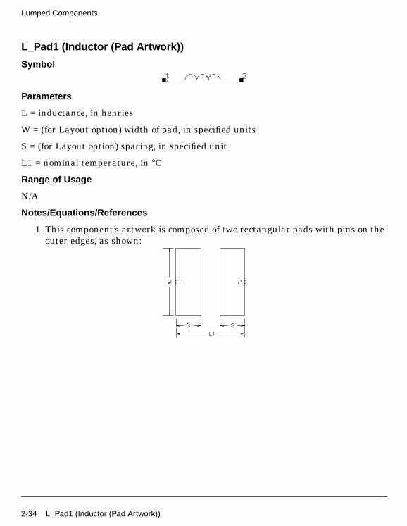
L_Pad1 (Inductor (Pad Artwork))
Symbol
Parameters
L = inductance, in henries
W = (for Layout option) width of pad, in specified units
S = (for Layout option) spacing, in specified unit
L1 = nominal temperature, in °C
Range of Usage
N/A
Notes/Equations/References
1. This component’s artwork is composed of two rectangular pads with pins on theouter edges, as shown:
2-34 L_Pad1 (Inductor (Pad Artwork))

L_Space (Inductor (Space Artwork))
Symbol
Parameters
L = inductance, in henries
L1 = nominal temperature, in °C
Range of Usage
N/A
Notes/Equations/References
1. This component is represented as a connected gap in layout—into which acustom artwork object can be inserted.
L_Space (Inductor (Space Artwork)) 2-35

Lumped Components
LQ_Conn (Inductor with Q (Connector Artwork))
Symbol
Parameters
L = inductance, in henries
Q = quality factor
F = reference frequency for Q
Mode = frequency dependence mode of Q; options (also see notes):
1 is proportional to freq
2 is proportional to sqrt(freq)
3 is constant
Temp = temperature, in °C
Range of Usage
F ≥ 0
Notes/Equations/References
1.
where:
Mode Setting Q G
proportional to freq Q(f) = Q(F) × f/F G(f) = G(F)
proportional to sqrt (freq) Q(f) = Q(F) × G(f) = G(F) ×
constant Q(f) = Q(F) G(f) = G(F) × f/F
If F is set to zero, then Q is assumed to be infinite.
where
f = simulation frequencyF = reference frequencyG = conductance of capacitor
Q 2πfLR
-------------=
f F⁄ f F⁄
2-36 LQ_Conn (Inductor with Q (Connector Artwork))

2. For time-domain analysis, the frequency-domain analytical model is used.
3. This component is a single connection in layout. For example, it can be used torepresent parasitics.
Equivalent Circuit
LQ_Conn (Inductor with Q (Connector Artwork)) 2-37

Lumped Components
LQ_Pad1 (Inductor with Q (Pad Artwork))
Symbol
Parameters
L = inductance, in henries
Q = quality factor
F = reference frequency for Q
Mode = loss mode for this device; options (also see notes):
1 is proportional to freq
2 is proportional to sqrt(freq)
3 is constant
Temp = temperature, in °C
W = (for Layout option) width of pad, in specified units
S = (for Layout option) spacing, in specified units
L1 = (for Layout option) pin-to-pin distance, in specified units
Range of Usage
F ≥ 0
Notes/Equations/References
1.
where:
Mode Setting Q G
proportional to freq Q(f) = Q(F) × f/F G(f) = G(F)
proportional to sqrt (freq) Q(f) = Q(F) × G(f) = G(F) ×
Q 2πfLR
-------------=
f F⁄ f F⁄
2-38 LQ_Pad1 (Inductor with Q (Pad Artwork))

2. For time-domain analysis, the frequency-domain analytical model is used.
3. This component’s artwork is composed of two rectangular pads with pins on theouter edges, as shown:
Equivalent Circuit
constant Q(f) = Q(F) G(f) = G(F) × f/F
If F is set to zero, then Q is assumed to be infinite.
where
f = simulation frequencyF = reference frequencyG = conductance of capacitor
Mode Setting Q G
LQ_Pad1 (Inductor with Q (Pad Artwork)) 2-39

Lumped Components
LQ_Space (Inductor with Q (Space Artwork))
Symbol
Parameters
L = inductance, in henries
Q = quality factor
F = reference frequency for Q
Mode = loss mode for this device; options (also see notes):
1 is proportional to freq
2 is proportional to sqrt(freq)
3 is constant
Temp = temperature, in °C
L1 = (for Layout option) pin-to-pin distance, in specified units
Range of Usage
F ≥ 0
Notes/Equations/References
1.
where:
Mode Setting Q G
proportional to freq Q(f) = Q(F) × f/F G(f) = G(F)
proportional to sqrt (freq) Q(f) = Q(F) × G(f) = G(F) ×
constant Q(f) = Q(F) G(f) = G(F) × f/F
If F is set to zero, then Q is assumed to be infinite.
where
f = simulation frequencyF = reference frequencyG = conductance of capacitor
Q 2πfLR
-------------=
f F⁄ f F⁄
2-40 LQ_Space (Inductor with Q (Space Artwork))

2. For time-domain analysis, the frequency-domain analytical model is used.
3. This component is represented as a connected gap in layout—into which acustom artwork object can be inserted.
Equivalent Circuit
LQ_Space (Inductor with Q (Space Artwork)) 2-41

Lumped Components
Mutual (Mutual Inductor)
Symbol
Illustration:
Parameters
K = mutual inductor coupling coefficient
M = mutual inductance, in henries
Inductor1 = ID of inductor 1 (value type: string)
Inductor2 = ID of inductor 2 (value type: string)
Range of Usage
−1.0 ≤ K ≤ 1.0
Notes/Equations/References
1. Either K or M is to be specified, not both. If both are specified, M overrides K.
2. In the fields Inductor1 and Inductor2 enter the component names of any twoinductors whose mutual inductance is given as M. For example, the entriesInductor1= CMP4 and Inductor2 = CMP16 result in simulations that use thevalue M as mutual inductance between the inductors that appear on theschematic as CMP4 and CMP16. Use several mutual inductor components todefine other mutual inductances.
3. The ends of the inductors that are in phase are identified by a small open circleon the schematic symbol for the inductors.
2-42 Mutual (Mutual Inductor)

4. The mutual inductor component can be placed anywhere on the schematic, andthere is no limit to the number of mutual inductances that can be specified. Ithas no effect on auto-layout.
Mutual (Mutual Inductor) 2-43

Lumped Components
PLC (Parallel Inductor-Capacitor)
Symbol
Parameters
L = inductance, in henries
C = capacitance in farads
Range of Usage
Use for high Q circuits rather than individual components in parallel.
Notes/Equations/References
1. This component has no default artwork associated with it.
Equivalent Circuit
2-44 PLC (Parallel Inductor-Capacitor)

PLCQ (Parallel Inductor-Capacitor with Q)
Symbol
Parameters
L = capacitance, in farads
Ql = quality factor of inductor
Fl = frequency at which Q is defined, in hertz
Mode =frequency dependence mode of inductor Q; options (also see notes):
1 is proportional to freq
2 is proportional to sqrt(freq)
3 is constant
C = capacitance, in farads
Qc = quality factor of capacitor
Fc = frequency at which capacitor Q is given, in hertz
ModC = frequency dependence mode of capacitor Q; options (also see notes):proportional to freq; proportional to sqrt(freq); constant; (value type: enumerated)
Rdc = resistance for modes 2 and 3
Range of Usage
Use for high Q circuits, rather than individual components in parallel.
Notes/Equations/References
1. (for inductors) (for capacitors)Ql2π f sL
R-----------------= Qc
2π f sC
G-----------------=
PLCQ (Parallel Inductor-Capacitor with Q) 2-45

Lumped Components
where
2. For time-domain analysis, the frequency-domain analytical model is used.
3. This component has no default artwork associated with it.
Equivalent Circuit
ModL Setting Ql ModC Setting Ql Qc
proportional to freq Ql(Fl) × fs/Fl proportional to freq Qc(Fc) × fs/Fc
proportional to sqrt(freq)
Q(f) = Q(F) × G(f) = G(F) × proportional tosqrt (freq)
constant Ql(Fl) constant Qc(Fc)
where
R = resistance of inductorG= conductance of capacitorfs = simulation frequencyFc, Fl = specified Q frequencies
f F⁄f F⁄
2-46 PLCQ (Parallel Inductor-Capacitor with Q)
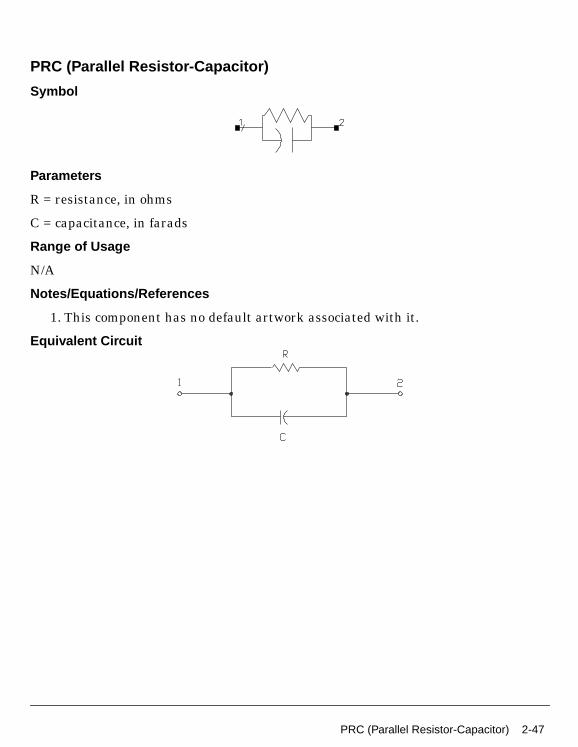
PRC (Parallel Resistor-Capacitor)
Symbol
Parameters
R = resistance, in ohms
C = capacitance, in farads
Range of Usage
N/A
Notes/Equations/References
1. This component has no default artwork associated with it.
Equivalent Circuit
PRC (Parallel Resistor-Capacitor) 2-47

Lumped Components
PRL (Parallel Resistor-Inductor)
Symbol
Parameters
R = resistance, in ohms
C = capacitance, in henries
Range of Usage
N/A
Notes/Equations/References
1. This component has no default artwork associated with it.
Equivalent Circuit
2-48 PRL (Parallel Resistor-Inductor)

PRLC (Parallel Resistor-Inductor-Capacitor)
Symbol
Parameters
R = resistance, in ohms
L = inductance, in henries
C = capacitance, in farads
Range of Usage
Use with high Q circuits, rather than individual components in parallel.
Notes/Equations/References
1. This component has no default artwork associated with it.
Equivalent Circuit
PRLC (Parallel Resistor-Inductor-Capacitor) 2-49

Lumped Components
R (Resistor)
Symbol
Parameters
R = resistance, in ohms (default: 50 ohms)
Temp = temperature, in °C
Tnom = nominal temperature, in °C
TC1 = linear temperature coefficient, in 1/°C
TC2 = quadratic temperature coefficient, in 1/°C2
Noise = resistor thermal noise option: YES=enable; NO=disable
wPmax = maximum power dissipation (warning), in watts
wImax = maximum current (warning), in amperes
Model = name of a resistor model to use
Width = physical width for use with a model
Length = physical length for use with a model
_M = number of resistors in parallel (default: 1)
Range of Usage
N/A
Notes/Equations/References
1. The resistor value can be made a function of temperature by setting Tnom andeither TC1 or TC2 or both. Tnom specifies the nominal temperature at which Ris given. Tnom defaults to 25°C. If Temp≠Tnom, then the simulated resistancevalue is given by:
R′ = R × [1 + TC1 (Temp − Tnom) + TC2 (Temp − Tnom)2]
2. If Temp is not explicitly specified, it defaults to the global temperature specifiedin the options item.
3. The resistor generates thermal noise:
<i2> = 4kT/R
2-50 R (Resistor)

Noise generation can be disabled by setting Noise=NO.
4. wPmax and wImax are used by the overload alert feature. They set limits onthe maximum instantaneous power dissipated by the resistor and maximumcurrent through the resistor. If these limits are specified, the simulator willissue a warning the first time they are exceeded during a dc, harmonic balanceor transient simulation. Simulation results are not affected by this parameter.
5. For a transient simulation, the resistance can vary with time. The resistancevalue should be assigned an expression that is a function of the reservedvariable time, which is the simulation time in seconds.
6. If a model name is given, then values that are not specified on the resistorinstance are taken from the model values. Typical values that can be defaultedare resistance, length and width, nominal temperature, temperaturecoefficients, and overload alert parameters.
If a model is used, the resistance value to be simulated (before temperaturescaling is applied) is computed as:
R′ = R + Rsh × (Length −2 × Narrow) / (Width −2 × Narrow)
7. _M is used to represent the number of resistors in parallel and defaults to 1. Mcannot be zero. If a resistor model is used, an optional scaling parameter Scalecan also be defined on the model; it defaults to 1. The effective resistance thatwill be simulated is R*Scale/M.
R (Resistor) 2-51
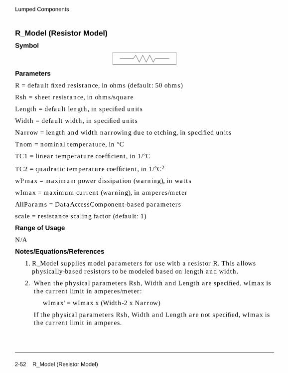
Lumped Components
R_Model (Resistor Model)
Symbol
Parameters
R = default fixed resistance, in ohms (default: 50 ohms)
Rsh = sheet resistance, in ohms/square
Length = default length, in specified units
Width = default width, in specified units
Narrow = length and width narrowing due to etching, in specified units
Tnom = nominal temperature, in °C
TC1 = linear temperature coefficient, in 1/°C
TC2 = quadratic temperature coefficient, in 1/°C2
wPmax = maximum power dissipation (warning), in watts
wImax = maximum current (warning), in amperes/meter
AllParams = DataAccessComponent-based parameters
scale = resistance scaling factor (default: 1)
Range of Usage
N/A
Notes/Equations/References
1. R_Model supplies model parameters for use with a resistor R. This allowsphysically-based resistors to be modeled based on length and width.
2. When the physical parameters Rsh, Width and Length are specified, wImax isthe current limit in amperes/meter:
wImax' = wImax x (Width-2 x Narrow)
If the physical parameters Rsh, Width and Length are not specified, wImax isthe current limit in amperes.
2-52 R_Model (Resistor Model)

3. Use AllParams with a DataAccessComponent to specify file-based parameters(refer to DataAccessComponent). Note that model parameters that areexplicitly specified take precedence over those specified via AllParams.
R_Model (Resistor Model) 2-53
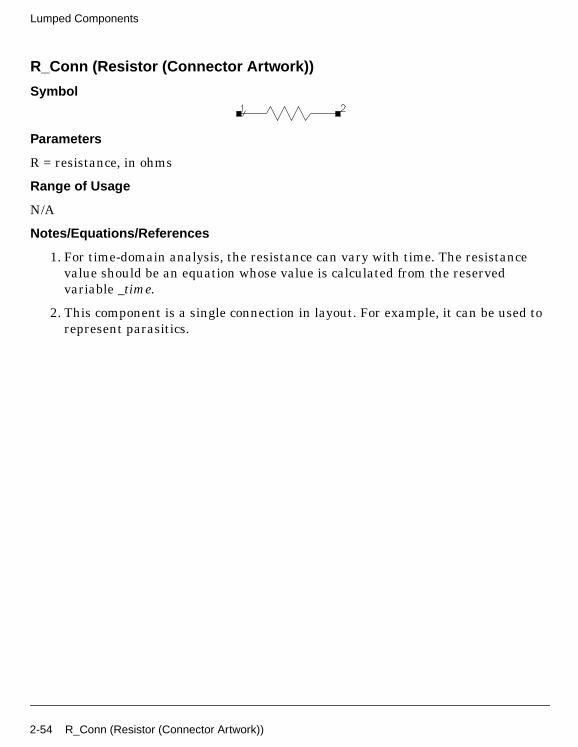
Lumped Components
R_Conn (Resistor (Connector Artwork))
Symbol
Parameters
R = resistance, in ohms
Range of Usage
N/A
Notes/Equations/References
1. For time-domain analysis, the resistance can vary with time. The resistancevalue should be an equation whose value is calculated from the reservedvariable _time.
2. This component is a single connection in layout. For example, it can be used torepresent parasitics.
2-54 R_Conn (Resistor (Connector Artwork))

R_Pad1 (Resistor (Pad Artwork))
Symbol
Parameters
R = resistance, in ohms
W = (for Layout option) width of pad, in specified units
S = (for Layout option) spacing, in specified units
L1 = (for Layout option) pin-to-pin distance, in specified units
Range of Usage
N/A
Notes/Equations/References
1. For transient and convolution analyses, resistance can vary with time. Theresistance value should be an equation whose value is calculated from thereserved variable _time.
2. This component’s artwork is composed of two rectangular pads with pins on theouter edges, as shown:
R_Pad1 (Resistor (Pad Artwork)) 2-55
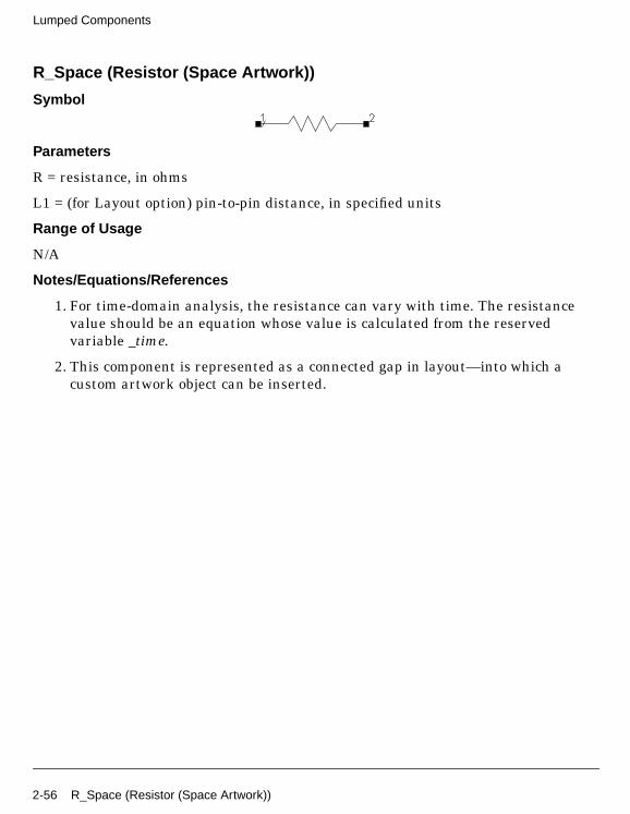
Lumped Components
R_Space (Resistor (Space Artwork))
Symbol
Parameters
R = resistance, in ohms
L1 = (for Layout option) pin-to-pin distance, in specified units
Range of Usage
N/A
Notes/Equations/References
1. For time-domain analysis, the resistance can vary with time. The resistancevalue should be an equation whose value is calculated from the reservedvariable _time.
2. This component is represented as a connected gap in layout—into which acustom artwork object can be inserted.
2-56 R_Space (Resistor (Space Artwork))

Short (Short)
Symbol
Parameters
Mode = mode: short, dc block, dc feed (value type: integer)
C = dc block capacitance, in farads
L = dc feed inductance, in henries
Gain = current gain
SaveCurrent = save branch current (default: no
wImax = maximum current warning, in amperes (value type: real)
Range of Usage
N/A
Notes/Equations/References
1. This component behaves like a current probe. It can be used to measure thecurrent anywhere in the circuit.
2. The variable name for the current is label.i, where label is the label of thiscomponent.
Short (Short) 2-57
Lumped Components
SLC (Series Inductor-Capacitor)
Symbol
Parameters
L = inductance, in henries
C = capacitance, in farads
Range of Usage
Use when modeling high Q circuits as opposed to two individual components.
Notes/Equations/References
1. This component has no default artwork associated with it.
2-58 SLC (Series Inductor-Capacitor)

SLCQ (Series Inductor-Capacitor with Q)
Symbol
Parameters
L = inductance, in henries
Ql = quality factor of inductor
Fl = frequency at which Q is defined, in hertz
ModL =frequency dependence mode of inductor Q; options (also see notes):
1 is proportional to freq
2 is proportional to sqrt(freq)
3 is constant
C = capacitance, in farads
Qc = quality factor of capacitor
Fc = frequency at which capacitor Q is given, in hertz
ModC =frequency dependence mode of capacitor Q; options (also see notes):
1 is proportional to freq
2 is proportional to sqrt(freq)
3 is constant
Rdc = resistance for modes 2 and 3
Range of Usage
Use when modeling high Q circuits rather than individual components in series.
Notes/Equations/References
1. (for inductors) (for capacitors)Ql2π f sL
R-----------------= Qc
2π f sC
G-----------------=
SLCQ (Series Inductor-Capacitor with Q) 2-59

Lumped Components
where
2. For time-domain analysis, the frequency-domain analytical model is used.
3. This component has no default artwork associated with it.
Equivalent Circuit
ModL Setting Ql ModC Setting Qc
proportional to freq Ql(Fl) × fs/Fl proportional to freq Qc(Fc) × fs/Fc
proportional to sqrt(freq) Ql(Fl) × proportional to sqrt(freq) Qc(Fc) ×
constant Ql(Fl) constant Qc(Fc)
where
R = resistance of inductorG= conductance of capacitorfs = simulation frequencyFc, Fl = specified Q frequencies
f s Fl⁄f s Fc⁄
2-60 SLCQ (Series Inductor-Capacitor with Q)

SMT_Pad (SMT Bond Pad)
Symbol
Illustration
Parameters
W = width of pad, in specified units
L = length of pad, in specified units
PadLayer = layer of pad: default, cond, cond2, resi, diel, diel2, hole, bond, symbol,text, leads, packages; (value type: enumerated)
SMO = solder mask overlap, in specified units
SM_Layer = solder mask layer: solder_mask, hole, bond, symbol, text, leads,packages, ports, bound, silk_screen, silk_screen2, case_dimensions; (value type:enumerated)
PO = pad offset from connection pin, in specified units
Range of Usage
W ≥ 0
L ≥ 0
Notes/Equations/References
1. This component is required for layout of SMT library parts.
2. For any library item to which this component is attached, the PO parameterspecifies the offset of the bond pad center from the position of pin connectionsdesignated for that item’s package artwork. An offset of 0 centers the padaround the location of the pins. A positive value shifts the pad away from thepackage body; a negative value shifts the pad toward the package body.
W
SMO
SMT_Pad (SMT Bond Pad) 2-61

Lumped Components
3. A positive value for SMO increases the area of the solder mask; a negativevalue decreases it.
2-62 SMT_Pad (SMT Bond Pad)

SRC (Series Resistor-Capacitor)
Symbol
Parameters
R = inductance, in ohms
C = capacitance, in farads
Range of Usage
N/A
Notes/Equations/References
1. This component has no default artwork associated with it.
SRC (Series Resistor-Capacitor) 2-63

Lumped Components
SRL (Series Resistor-Inductor)
Symbol
Parameters
R = resistance, in ohms
C = inductance, in henries
Range of Usage
N/A
Notes/Equations/References
1. This component has no default artwork associated with it.
2-64 SRL (Series Resistor-Inductor)

SRLC (Series Resistor-Inductor-Capacitor)
Symbol
Parameters
R = resistance, in ohms
L = inductance, in henries
C = capacitance, in farads
Range of Usage
Use for high Q circuits, rather than individual components in parallel.
Notes/Equations/References
1. This component has no default artwork associated with it.
2-65

Lumped Components
TF (Transformer)
Symbol
Parameters
T = turns ratio T1/T2
Range of Usage
N/A
Notes/Equations/References
1. The turns ratio T is the ratio of turns in the primary to turns in the secondary(T:1).
A turns ratio less than 1 describes a transformer in which there are more turnsin the secondary than in the primary.
2. Parasitic inductances of the primary and secondary are not modeled. To do this,use the component for mutual inductance (M). The ends that are in phase areidentified by a small open circle on the schematic symbol.
3. Because this is an ideal transformer, the impedance transformation is the sameas the DC at nonzero frequencies.
4. This component passes DC.
2-66
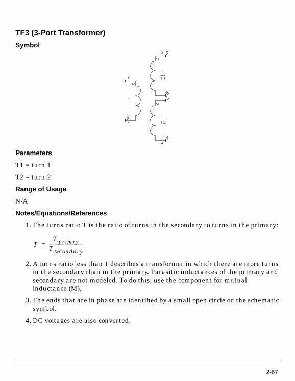
TF3 (3-Port Transformer)
Symbol
Parameters
T1 = turn 1
T2 = turn 2
Range of Usage
N/A
Notes/Equations/References
1. The turns ratio T is the ratio of turns in the secondary to turns in the primary:
2. A turns ratio less than 1 describes a transformer in which there are more turnsin the secondary than in the primary. Parasitic inductances of the primary andsecondary are not modeled. To do this, use the component for mutualinductance (M).
3. The ends that are in phase are identified by a small open circle on the schematicsymbol.
4. DC voltages are also converted.
TT primry
T ondarysec------------------------------=
2-67

Lumped Components
2-68

Chapter 3: Miscellaneous CircuitComponents
3-1
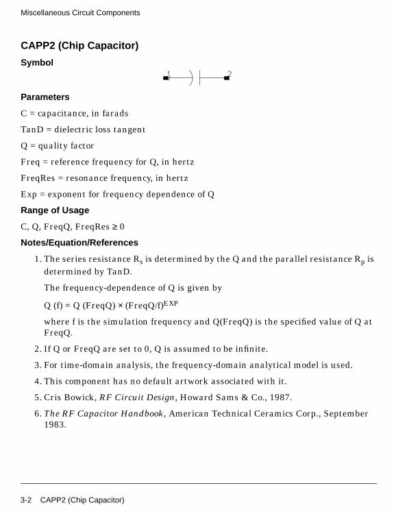
Miscellaneous Circuit Components
CAPP2 (Chip Capacitor)
Symbol
Parameters
C = capacitance, in farads
TanD = dielectric loss tangent
Q = quality factor
Freq = reference frequency for Q, in hertz
FreqRes = resonance frequency, in hertz
Exp = exponent for frequency dependence of Q
Range of Usage
C, Q, FreqQ, FreqRes ≥ 0
Notes/Equation/References
1. The series resistance Rs is determined by the Q and the parallel resistance Rp isdetermined by TanD.
The frequency-dependence of Q is given by
Q (f) = Q (FreqQ) × (FreqQ/f)EXP
where f is the simulation frequency and Q(FreqQ) is the specified value of Q atFreqQ.
2. If Q or FreqQ are set to 0, Q is assumed to be infinite.
3. For time-domain analysis, the frequency-domain analytical model is used.
4. This component has no default artwork associated with it.
5. Cris Bowick, RF Circuit Design, Howard Sams & Co., 1987.
6. The RF Capacitor Handbook, American Technical Ceramics Corp., September1983.
3-2 CAPP2 (Chip Capacitor)

Equivalent Circuit
CAPP2 (Chip Capacitor) 3-3

Miscellaneous Circuit Components
CIND (Ideal Torroidal Inductor)
Symbol
Illustration
Parameters
N = number of units
AL = inductance index
Range of Usage
N, AL > 0
Notes/Equation/References
1. The inductance is given by
L = N2 × AL
2. This component has no default artwork associated with it.
3-4 CIND (Ideal Torroidal Inductor)

RIND (Rectangular Inductor)
Symbol
Illustration
Parameters
N = number of turns (need not be an integer)
L1 = length of second outermost segment, in specified units
L2 = length of outermost segment, in specified units
W = conductor width, in specified units
S = conductor spacing, in specified units
T = conductor thickness, in specified units
Rho = conductor resistivity (relative to copper)
FR = resonant frequency, in hertz
Temp = physical temperature, in °C
Range of Usage
N must be such that all segments fit given L1, L2, W, and S.
Notes/Equation/References
1. For time-domain analysis, an impulse response obtained from thefrequency-domain analytical model is used.
RIND (Rectangular Inductor) 3-5

Miscellaneous Circuit Components
2. This component has no default artwork associated with it.
3. Greenhouse, H. M. “Design of Planar Rectangular Microelectronic Inductors,”IEEE Transactions as Parts, Hybrids, and Packaging, Vol. PHP-10, No. 2, June1974, pp. 101-109.
3-6 RIND (Rectangular Inductor)

XFERP (Physical Transformer)
Symbol
Parameters
N = turns ratio N1/N2
Lp = magnetizing inductance, in henries
Rc = core loss resistance, in ohms
K = coefficient of coupling
R1 = primary loss resistance, in ohms
R2 = secondary loss resistance, in ohms
C1 = primary capacitance, in farads
C2 = secondary capacitance, in farads
C = interwinding capacitance, in farads
Range of Usage
0 < K < 1
Notes/Equation/References
1. Primary leakage: L1 = LP
Secondary leakage: L2 =
2. This component has no default artwork associated with it.
1K----- 1–
L1
N2--------
XFERP (Physical Transformer) 3-7

Miscellaneous Circuit Components
Equivalent Circuit
3-8 XFERP (Physical Transformer)
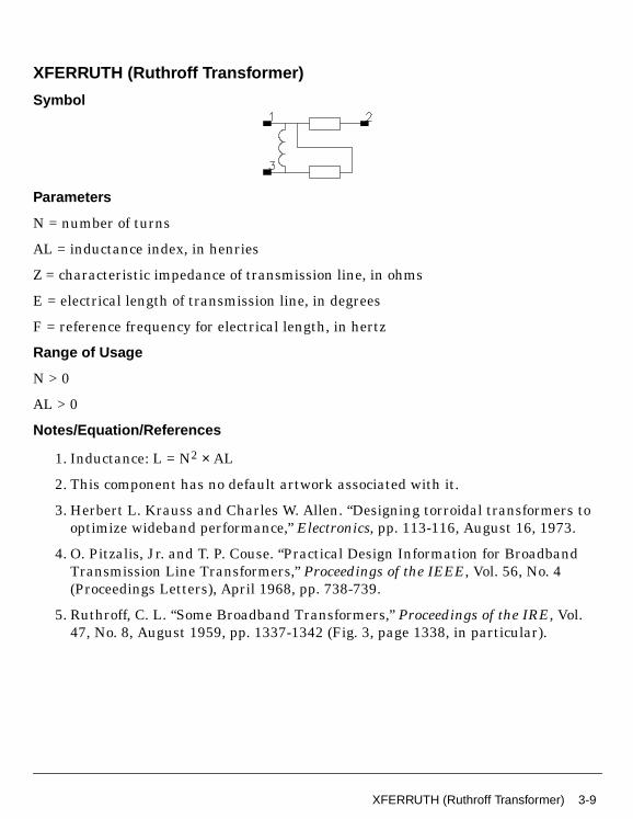
XFERRUTH (Ruthroff Transformer)
Symbol
Parameters
N = number of turns
AL = inductance index, in henries
Z = characteristic impedance of transmission line, in ohms
E = electrical length of transmission line, in degrees
F = reference frequency for electrical length, in hertz
Range of Usage
N > 0
AL > 0
Notes/Equation/References
1. Inductance: L = N2 × AL
2. This component has no default artwork associated with it.
3. Herbert L. Krauss and Charles W. Allen. “Designing torroidal transformers tooptimize wideband performance,” Electronics, pp. 113-116, August 16, 1973.
4. O. Pitzalis, Jr. and T. P. Couse. “Practical Design Information for BroadbandTransmission Line Transformers,” Proceedings of the IEEE, Vol. 56, No. 4(Proceedings Letters), April 1968, pp. 738-739.
5. Ruthroff, C. L. “Some Broadband Transformers,” Proceedings of the IRE, Vol.47, No. 8, August 1959, pp. 1337-1342 (Fig. 3, page 1338, in particular).
XFERRUTH (Ruthroff Transformer) 3-9
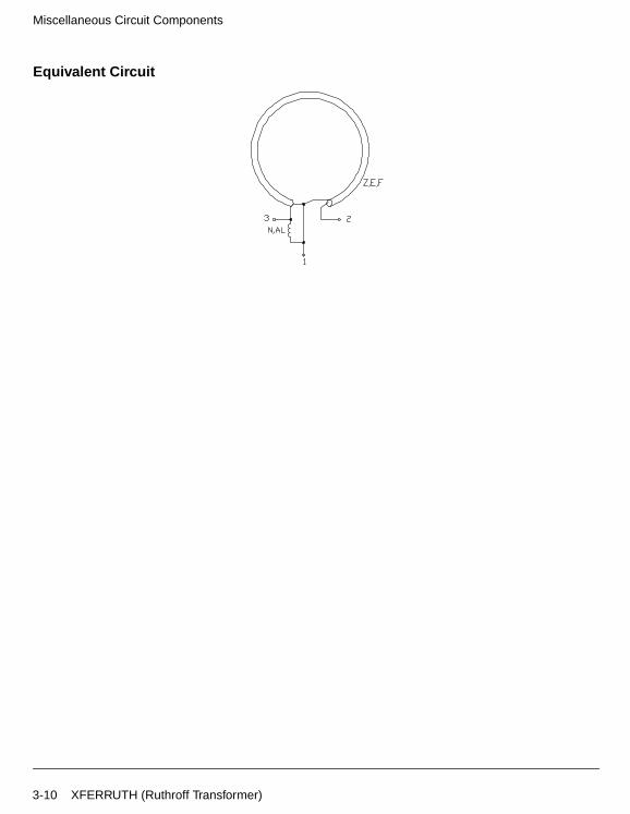
Miscellaneous Circuit Components
Equivalent Circuit
3-10 XFERRUTH (Ruthroff Transformer)

XFERTAP (Tapped Secondary Ideal Transformer)
Symbol
Parameters
N12 = turns ratio, N1/N2
N13 = turns ratio, N1/N3
L1 = primary winding inductance, in henries
K = coupling coefficient
Range of Usage
0 < K < 1
Notes/Equation/References
1. This component has no default artwork associated with it.
XFERTAP (Tapped Secondary Ideal Transformer) 3-11

Miscellaneous Circuit Components
3-12 XFERTAP (Tapped Secondary Ideal Transformer)

Chapter 4: Probe Components
4-1
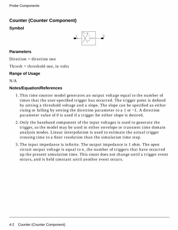
Probe Components
Counter (Counter Component)
Symbol
Parameters
Direction = direction one
Thresh = threshold one, in volts
Range of Usage
N/A
Notes/Equation/References
1. This time counter model generates an output voltage equal to the number oftimes that the user-specified trigger has occurred. The trigger point is definedby setting a threshold voltage and a slope. The slope can be specified as eitherrising or falling by setting the direction parameter to a 1 or −1. A directionparameter value of 0 is used if a trigger for either slope is desired.
2. Only the baseband component of the input voltages is used to generate thetrigger, so the model may be used in either envelope or transient time domainanalysis modes. Linear interpolation is used to estimate the actual triggercrossing time to a finer resolution than the simulation time step.
3. The input impedance is infinite. The output impedance is 1 ohm. The opencircuit output voltage is equal to n, the number of triggers that have occurredup the present simulation time. This count does not change until a trigger eventoccurs, and is held constant until another event occurs.
4-2 Counter (Counter Component)

I_Probe (Current Probe)
Symbol
Parameters
Mode = type of mode: short, dc block, dc feed (value type: integer)
C = dc block capacitance (transient only)
L = dc feed inductance (transient only)
Gain = current gain
SaveCurrent = save branch current (default: yes)
wImax = maximum current warning (value type: real)
Range of Usage
N/A
Notes/Equation/References
1. The positive current flow direction is assumed to be from pin 1 to pin 2.
2. To measure a branch current, an ammeter must be connected in that branchbefore performing the analysis.
3. This component has no default artwork associated with it.
I_Probe (Current Probe) 4-3

Probe Components
OscPort (Grounded Oscillator Port)
Symbol
Parameters
V = initial guess at fundamental voltage
Z = initial value for Z0, in ohms
NumOctaves = number of octaves to search
Steps = number of steps per search octave
FundIndex = fundamental number for oscillator
MaxLoopGainStep = maximum arc length continuation step size during loop-gainsearch
Range of Usage
N/A
Notes/Equation/References
1. This is a special device used for an oscillator analysis. Do not use more than oneoscillator port in a circuit.
2. NumOctaves specifies the total number of octaves over which the oscillatorsearch is done. Half of the octaves are below the initial frequency and half areabove. For example, if NumOctaves is 2, then the frequency search goes fromFreq/2 to Freq*2. Steps sets the number of frequency points per octave that areused in the search. For a high-Q oscillator, a large number of steps might berequired.
3. If no fundamental voltage V is specified, the simulator first performs asmall-signal AC analysis to determine the actual frequency and oscillationvoltage. If V is specified, it represents an initial guess at the fundamentaloscillator voltage at the point where the OscPort is inserted. The initial guessfor V should be as close to the actual value as possible. If it is not known, don’tspecify it. An inaccurate value increases the simulation time and might preventconvergence.
4-4 OscPort (Grounded Oscillator Port)

4. Provided the circuit produces at least one complex conjugate pole pair in theright-half-plane over the frequency range tested, the analysis will determinethe oscillation waveform and amplitude. Proper probe placement andimpedance can reduce the analysis time significantly and help ensure accurateoscillator analysis results. To reduce the probability of a failed analysis, placethe probe and set the initial impedance in a manner consistent with thefollowing guidelines:
Feedback Oscillators (such as Colpitts)
• Insert probe at a point in the feedback loop where the signal is contained to asingle path.
• Point the arrow of the probe in the direction of positive gain around the loop.
• Insert probe at a point in the feedback loop where source impedance is muchsmaller than load impedance (at least a factor of 10; a factor of 100 or more ispreferable).
• Point the arrow of the probe at the high impedance (load) node.
• Set the initial probe impedance (Z0) to a value approximately half-waybetween the source and load impedances presented by the circuit at the pointof insertion.
To minimize the analysis time, set the probe impedance to a factor of 10 belowthe load impedance, and a factor of 10 above the source impedance (providedthe source and load impedances are sufficiently far apart). Doing this effectivelyreduces to zero the dependence of the small signal loop gain on Z0.
Negative Resistance Oscillat ors
• Insert probe between a negative and positive impedance in the circuit. Thereshould be no other signal paths between these two parts of the circuit.Typically, the probe is inserted between the resonator and the effectivenegative resistance.
• You can point the arrow of the probe at either the negative impedance nodeor the positive impedance node.
• Set the initial probe impedance to any reasonable value. To minimize theanalysis time, it should be at least a factor of two higher or lower than themagnitude of the passive load impedance.
OscPort (Grounded Oscillator Port) 4-5

Probe Components
The frequency is specified on the harmonic balance analysis component. Thevalue for Z is chosen based on impedance levels in the circuit and the degree ofnon-linearity in the circuit. Do not use either 1 or 0 for Z as this will causeconvergence problems.
If the oscillator analysis fails, and this test indicates that the circuit shouldoscillate, the failure may be due to the fact that the circuit is too nonlinear. Thisproblem can sometimes be solved by trying different impedance values ofOscPort (determined by the Z attribute). Lower impedance values usually seemto work better. Also try reversing the OscPort direction.
Another approach is to try to get the oscillator to oscillate at some nicerparameter value and then to sweep the parameter value to the desired value.The parameter may be bias, self-bias impedance, some gain controlling value, oranother factor. In short, anything that will make the oscillator more linear, yetstill let it oscillate.
4-6 OscPort (Grounded Oscillator Port)

OscPort2 (Differential Oscillator Port)
Symbol
Parameters
Mode = oscillator mode: automatic, small signal loop gain, or large signal loop gain
V = initial guess at fundamental voltage (automatic mode only)
Z = initial value for Z0, in ohms (all modes)
NumOctaves = number of octaves to search (automatic mode only)
Steps = number of steps per search octave (automatic mode only)
FundIndex = fundamental number for oscillator (automatic mode only)
MaxLoopGainStep = maximum arc length continuation step size during loop-gainsearch (automatic mode only)
FreqPlan = sweep plan for frequency (small and large signal loop gain modes only)
VinjPlan = sweep plan for injected loop voltage (large signal loop gain mode only)
Range of Usage
N/A
Notes/Equation/References
1. This is a special device used for an oscillator analysis. Do not use more than oneoscillator test element (OscTest, OscPort, OscPort2) in a circuit.
2. NumOctaves specifies the total number of octaves over which the oscillatorsearch is done. Half of the octaves are below the initial frequency and half areabove. For example, if NumOctaves is 2, then the frequency search goes fromFreq/2 to Freq*2. Steps sets the number of frequency points per octave that areused in the search. For a high-Q oscillator, a large number of steps might berequired.
3. If no fundamental voltage V is specified, the simulator first performs asmall-signal AC analysis to determine the actual frequency and oscillationvoltage. If V is specified, it represents an initial guess at the fundamental
OscPort2 (Differential Oscillator Port) 4-7

Probe Components
oscillator voltage at the point where the OscPort is inserted. The initial guessfor V should be as close to the actual value as possible. If it is not known, don’tspecify it. An inaccurate value increases the simulation time and might preventconvergence.
4. This device can operate in one of three different modes. In automatic mode, it issimilar to the OscPort device, and is used with the harmonic balance oscillatoranalysis to determine the oscillator frequency, large signal solution andoptionally phase noise. In small signal loop gain mode, it is similar to theOscTest device, and is used to perform a small signal analysis of the oscillatorloop gain versus frequency. In large signal loop gain mode, it is used to simulatethe large signal nonlinear loop gain of the oscillator versus frequency andinjected loop voltage.
5. This device can be used for both single-ended and differential oscillatortopologies. For single-ended oscillators, the negative pins of this element shouldbe grounded. For differential oscillators, it should be connected differentiallyinto the oscillator loop.
6. Provided the circuit produces at least one complex conjugate pole pair in theright-half-plane over the frequency range tested, the analysis will determinethe oscillation waveform and amplitude. Proper probe placement andimpedance can reduce the analysis time significantly and help ensure accurateoscillator analysis results. To reduce the probability of a failed analysis, placethe probe and set the initial impedance in a manner consistent with thefollowing guidelines:
Feedback Oscillators (such as Colpitts)
• Insert probe at a point in the feedback loop where the signal is contained to asingle path.
• Point the arrow of the probe in the direction of positive gain around the loop.
• Insert probe at a point in the feedback loop where source impedance is muchsmaller than load impedance (at least a factor of 10; a factor of 100 or more ispreferable).
• Point the arrow of the probe at the high impedance (load) node.
• Set the initial probe impedance (Z0) to a value approximately half-waybetween the source and load impedances presented by the circuit at the pointof insertion.
4-8 OscPort2 (Differential Oscillator Port)

To minimize the analysis time, set the probe impedance to a factor of 10 belowthe load impedance, and a factor of 10 above the source impedance (providedthe source and load impedances are sufficiently far apart). Doing this effectivelyreduces to zero the dependence of the small signal loop gain on Z0.
Negative Resistance Oscillators
• Insert probe between a negative and positive impedance in the circuit. Thereshould be no other signal paths between these two parts of the circuit.Typically, the probe is inserted between the resonator and the effectivenegative resistance.
• You can point the arrow of the probe at either the negative impedance nodeor the positive impedance node.
• Set the initial probe impedance to any reasonable value. To minimize theanalysis time, it should be at least a factor of two higher or lower than themagnitude of the passive load impedance.
The frequency is specified on the harmonic balance analysis component. Thevalue for Z is chosen based on impedance levels in the circuit and the degree ofnon-linearity in the circuit. Do not use either 1 or 0 for Z as this will causeconvergence problems.
If the oscillator analysis fails, and this test indicates that the circuit shouldoscillate, the failure may be due to the fact that the circuit is too nonlinear. Thisproblem can sometimes be solved by trying different impedance values ofOscPort (determined by the Z attribute). Lower impedance values usually seemto work better. Also try reversing the OscPort direction.
Another approach is to try to get the oscillator to oscillate at some nicerparameter value and then to sweep the parameter value to the desired value.The parameter may be bias, self-bias impedance, some gain controlling value, oranother factor. In short, anything that will make the oscillator more linear, yetstill let it oscillate.
OscPort2 (Differential Oscillator Port) 4-9
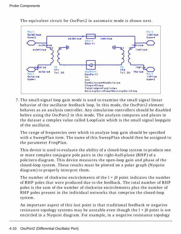
Probe Components
The equivalent circuit for OscPort2 in automatic mode is shown next.
7. The small-signal loop gain mode is used to examine the small signal linearbehavior of the oscillator feedback loop. In this mode, the OscPort2 elementbehaves as an analysis controller. Any simulation controllers should be disabledbefore using the OscPort2 in this mode. The analysis computes and places inthe dataset a complex value called LoopGain which is the small signal loopgainof the oscillator.
The range of frequencies over which to analyze loop gain should be specifiedwith a SweepPlan item. The name of this SweepPlan should then be assigned tothe parameter FreqPlan.
This device is used to evaluate the ability of a closed-loop system to produce oneor more complex conjugate pole pairs in the right-half-plane (RHP) of apole/zero diagram. This device measures the open-loop gain and phase of theclosed-loop system. These results must be plotted on a polar graph (Nyquistdiagram) to properly interpret them.
The number of clockwise encirclements of the l + j0 point indicates the numberof RHP poles that were produced due to the feedback. The total number of RHPpoles is the sum of the number of clockwise encirclements plus the number ofRHP poles present in the individual networks that comprise the closed-loopsystem.
An important aspect of this last point is that traditional feedback or negativeresistance topology systems may be unstable even though the l + j0 point is notencircled in a Nyquist diagram. For example, in a negative resistance topology
4-10 OscPort2 (Differential Oscillator Port)
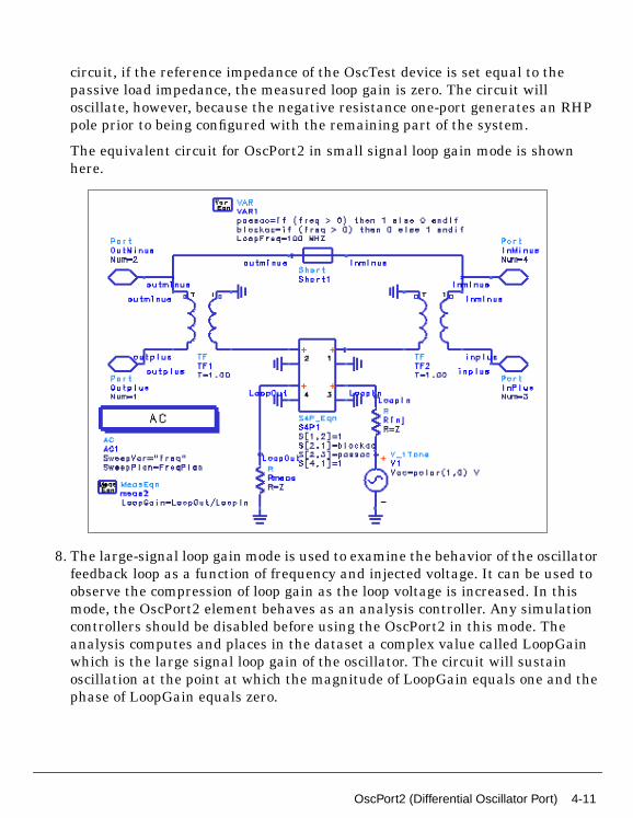
circuit, if the reference impedance of the OscTest device is set equal to thepassive load impedance, the measured loop gain is zero. The circuit willoscillate, however, because the negative resistance one-port generates an RHPpole prior to being configured with the remaining part of the system.
The equivalent circuit for OscPort2 in small signal loop gain mode is shownhere.
8. The large-signal loop gain mode is used to examine the behavior of the oscillatorfeedback loop as a function of frequency and injected voltage. It can be used toobserve the compression of loop gain as the loop voltage is increased. In thismode, the OscPort2 element behaves as an analysis controller. Any simulationcontrollers should be disabled before using the OscPort2 in this mode. Theanalysis computes and places in the dataset a complex value called LoopGainwhich is the large signal loop gain of the oscillator. The circuit will sustainoscillation at the point at which the magnitude of LoopGain equals one and thephase of LoopGain equals zero.
OscPort2 (Differential Oscillator Port) 4-11

Probe Components
The range of frequencies over which to analyze loop gain should be specifiedwith a SweepPlan item. The name of this SweepPlan should then be assigned tothe parameter FreqPlan.
The range of voltages over which to analyze loop gain should be specified with aSweepPlan item. The name of this SweepPlan should then be assigned to theparameter VinjPlan. Initially the sweep should be done with a logarithmicsweep to determine where the oscillator loop goes into compression. Once thisrange is estimated, a linear sweep can be done to zero in north injected voltagethat causes oscillation to be sustained.
A useful way to interpret results from this analysis is to plot the phase ofLoopGain against LoopGain in decibels. Lines of constant frequency will beplotted with values at each voltage value. The circuit will oscillate at thefrequency and voltage associated with the (0,0) point on the graph.
The equivalent circuit for OscPort2 in large signal loop gain mode is shownhere.
In both small signal and large signal loop gain modes, this element injects a testsignal into an oscillator circuit for stimulating oscillations. The specialized
4-12 OscPort2 (Differential Oscillator Port)

directional coupler has zero electrical length and is invisible to normal circuitsimulation. It injects a fundamental frequency test signal, blocks thefundamental frequency flow in the feedback path, monitors the signal returnedby the feedback path and computes the loop gain.
The directional coupler in loop gain mode (both small and large signal) isdesigned to allow the injection of a test signal from port 3 to port 2 as the loopinput and to pass the loop output from port 1 to port 4. It does this only at thesignal frequency: the AC frequency for small signal loop gain and thefundamental tone for large signal loop gain. All other frequencies, including DC,are coupled from port 1 to port 2.
The scattering matrices follow.
SFUNDAMENTAL
0 1 0 0
0 0 1 0
0 0 0 0
1 0 0 0
=
SOTHER
0 1 0 0
1 0 0 0
0 0 0 0
1 0 0 0
=
OscPort2 (Differential Oscillator Port) 4-13
Probe Components
OscTest (Grounded Oscillator Test)
Symbol
Parameters
Port_Number = port number
Z = initial value for Z0, in ohms
Start = start frequency, in hertz
Stop = stop frequency, in hertz
Points = number of frequency points
Range of Usage
N/A
Notes/Equation/References
1. This device is used to evaluate the ability of a closed-loop system to produce oneor more complex conjugate pole pairs in the right-half-plane (RHP) of apole/zero diagram. This device measures the open-loop gain and phase of theclosed-loop system. These results must be plotted on a polar graph (Nyquistdiagram) to properly interpret them.
The number of clockwise encirclements of the l + j0 point indicates the numberof RHP poles that were produced due to the feedback. The total number of RHPpoles is the sum of the number of clockwise encirclements plus the number ofRHP poles present in the individual networks that comprise the closed-loopsystem.
An important aspect of this last point is that traditional feedback or negativeresistance topology systems may be unstable even though the l + j0 point is notencircled in a Nyquist diagram. For example, in a negative resistance topologycircuit, if the reference impedance of the OscTest device is set equal to thepassive load impedance, the measured loop gain is zero. The circuit willoscillate, however, because the negative resistance one-port generates an RHPpole prior to being configured with the remaining part of the system.
4-14 OscTest (Grounded Oscillator Test)
TimeDelta (Time Delta Component)
Symbol
Parameters
Direction1 = direction one
Direction2 = direction two
Thresh1 = threshold one, in volts
Thresh2 = threshold two, in volts
Scale = scale factor
Range of Usage
N/A
Notes/Equation/References
1. TimeDelta generates an output voltage proportional to the time differencebetween two trigger points on two different baseband input voltage waveforms.The trigger points are user-defined by setting a threshold voltage and a slope.The slope can be specified as either rising or falling by setting the directionparameter to a 1 or −1. A direction parameter value of 0 is used if a trigger foreither slope is desired.
2. Only the baseband component of the input voltages are used to generate thetriggers, so this model can be used in either envelope or transient time domainanalysis modes. Linear interpolation is used to estimate the actual triggercrossing time to a finer resolution than the simulation time step.
3. The input impedances are infinite. The output impedance is 1 ohm. The opencircuit output voltage is equal to the time difference between the trigger2 andtrigger1 events, multiplied by the scaling factor. The output does not changeuntil a trigger2 event occurs and is held constant until another trigger2 eventoccurs. The scaling factor is used so that the output voltages can be set toreasonable values (i.e., not nanovolts) which would often be less than thesimulator’s absolute convergence criteria.
TimeDelta (Time Delta Component) 4-15

Probe Components
4. Several example measurements possible with this model might be the input tooutput propagation delay of a circuit, the -40 to +20 dBm rise time of ademodulated RF pulse, various fall times, pulse widths, etc. The output voltagecan be used for other behavioral models, for optimization, or for output topresentations.
4-16 TimeDelta (Time Delta Component)

TimeFrq (Time Frequency Component)
Symbol
Parameters
Direction = direction one
Thresh = threshold one, in volts
Scale = scale factor
Range of Usage
N/A
Notes/Equation/References
None
TimeFrq (Time Frequency Component) 4-17

Probe Components
TimePeriod (Time Period Component)
Symbol
Parameters
Direction = direction one
Thresh = threshold one, in volts
Scale = scale factor
Range of Usage
N/A
Notes/Equation/References
1. This time period model generates an output voltage proportional to the timebetween two consecutive triggers. The trigger point is defined by setting athreshold voltage and a slope. The slope can be specified as either rising orfalling by setting the direction parameter to a 1 or −1. A direction parametervalue of 0 is used if a trigger for either slope is desired.
2. Only the baseband component of the input voltages is used to generate thetrigger, so this model may be used in either envelope or transient time domainanalysis modes. Linear interpolation is used to estimate the actual triggercrossing time to a significantly higher resolution than the simulation time step.
3. The input impedance is infinite. The output impedance is 1 ohm. The opencircuit output voltage is equal to the time difference between the last twotrigger events multiplied by the scaling factor. The output does not change untila trigger event occurs and is held constant until another event occurs. Thescaling factor is used so that the output voltage can be set to reasonable valuewhich might otherwise be less than the simulator’s absolute convergencecriteria.
4-18 TimePeriod (Time Period Component)

TimeStamp (Time Stamp Component)
Symbol
Parameters
Direction = direction one
Thresh = threshold one, in volts
Scale = scale factor
Range of Usage
N/A
Notes/Equation/References
1. TimeStamp generates an output voltage proportional to the time that the lastuser-defined trigger occurred. The trigger point is defined by setting a thresholdvoltage and a slope. The slope can be specified as either rising or falling bysetting the direction parameter to a 1 or −1. A direction parameter value of 0 isused if a trigger for either slope is desired.
2. Only the baseband component of the input voltages is used to generate thetrigger, so the model may be used in either envelope or transient time analysismodes. Linear interpolation is used to estimate the actual trigger crossing timeto a significantly higher resolution than the simulation time step domain.
3. The input impedance is infinite. The output impedance is 1 ohm. The opencircuit output voltage is equal to the time of the last trigger event multiplied bythe scaling factor. The output does not change until a trigger event occurs and isheld constant until another event occurs. The scaling factor is used so that theoutput voltage can be set to a reasonable value which might otherwise be lessthan the simulator’s absolute convergence criteria.
TimeStamp (Time Stamp Component) 4-19

Probe Components
WaveformStats (WaveformStats Component)
Symbol
Parameters
None
Range of Usage
N/A
Notes/Equation/References
1. This behavioral model can be used to measure the statistics of the basebandcomponent of the input voltage. The three inputs all have infinite inputimpedance. All six outputs are ideal voltage sources with zero outputimpedance.
2. If the enable is low during a reset, then the accumulators are reset to 0. If theenable is high, then N is set to one, and Sum is set equal to the input.
3. In addition to making gated, statistical measurements for use in optimizationsor presentations, you can use this device to model circuits such as idealintegrate-and-dump circuits or peak detector circuits.
4. To measure the statistics of an RF carrier in circuit envelope mode, the correctdemodulator must first be used to create a baseband voltage that can then beused as an input to this device.
5. This model operates in transient and envelope time domain analysis modes.
4-20 WaveformStats (WaveformStats Component)
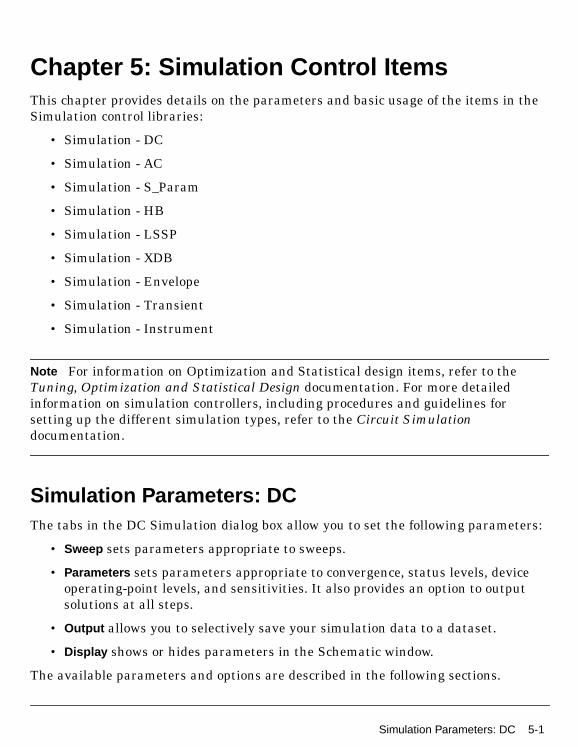
Chapter 5: Simulation Control ItemsThis chapter provides details on the parameters and basic usage of the items in theSimulation control libraries:
• Simulation - DC
• Simulation - AC
• Simulation - S_Param
• Simulation - HB
• Simulation - LSSP
• Simulation - XDB
• Simulation - Envelope
• Simulation - Transient
• Simulation - Instrument
Note For information on Optimization and Statistical design items, refer to theTuning, Optimization and Statistical Design documentation. For more detailedinformation on simulation controllers, including procedures and guidelines forsetting up the different simulation types, refer to the Circuit Simulationdocumentation.
Simulation Parameters: DCThe tabs in the DC Simulation dialog box allow you to set the following parameters:
• Sweep sets parameters appropriate to sweeps.
• Parameters sets parameters appropriate to convergence, status levels, deviceoperating-point levels, and sensitivities. It also provides an option to outputsolutions at all steps.
• Output allows you to selectively save your simulation data to a dataset.
• Display shows or hides parameters in the Schematic window.
The available parameters and options are described in the following sections.
Simulation Parameters: DC 5-1

Simulation Control Items
Sweep
Parameter to sweep
Use this field to enter a defined parameter (for example, DC supply voltage).
Parameter sweep
Use this area to select from a variety of sweep types and other parameters.
Sweep Type
Single point selects a specific value for a parameter.
Linear provides for a linear sweep. Click the Start/Stop button (see below) to selectthe start and stop values for the sweep.
Log provides for a logarithmic sweep. The Center/Span button (see below) does notapply to a logarithmic sweep.
Start/Stop selects start and stop points for a sweep.
Center/Span selects the center and span of a sweep.
Start is the start point of a sweep.
Stop is the stop point of a sweep.
Step-size is the size of each step.
Num. of pts. is the number of points over which the sweep is conducted.
Note A change to one of the preceding four fields causes the remaining fields to becalculated automatically.
Use Sweep Plan
To use a sweep plan (SweepPlan) component that you have defined and named, selectthis option and enter the name of the plan in the field.
5-2

Note To shorten simulation time in any parameter sweep, select a start point asclose as possible to the convergence point and vary the parameter gradually. Thisyields better estimates for the next simulation, and achieves convergence morerapidly than if the parameter were changed abruptly.
Parameters
Convergence
Use this area to edit the following parameters:
Max. delta V is the maximum change in node voltage allowed per iteration. If novalue is specified, the default value is four times the thermal voltage, orapproximately 0.1 V.
Max. iterations is the maximum number of iterations to be performed. Thesimulation will iterate until it converges, an error occurs, or this limit is reached.
Mode
Use this popup menu to select a convergence algorithm.
Note The following DC convergence options are also available in the Optionscomponent, under the Convergence tab. Use the Options component to setparameters applicable to all analyses in a Schematic window.
Auto sequence is the default mode.
Quick convergence test uses results from initial tests to help predict whichcombinations of convergence parameters should be tested. This mode starts byapplying the Newton-Raphson algorithm for several values of Max. delta V.
5-3
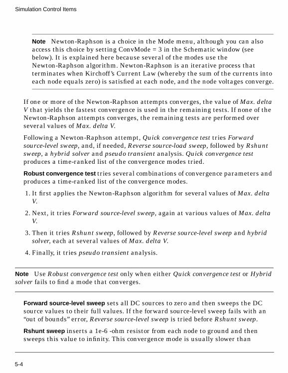
Simulation Control Items
Note Newton-Raphson is a choice in the Mode menu, although you can alsoaccess this choice by setting ConvMode = 3 in the Schematic window (seebelow). It is explained here because several of the modes use theNewton-Raphson algorithm. Newton-Raphson is an iterative process thatterminates when Kirchoff ’s Current Law (whereby the sum of the currents intoeach node equals zero) is satisfied at each node, and the node voltages converge.
If one or more of the Newton-Raphson attempts converges, the value of Max. deltaV that yields the fastest convergence is used in the remaining tests. If none of theNewton-Raphson attempts converges, the remaining tests are performed overseveral values of Max. delta V.
Following a Newton-Raphson attempt, Quick convergence test tries Forwardsource-level sweep, and, if needed, Reverse source-load sweep, followed by Rshuntsweep, a hybrid solver and pseudo transient analysis. Quick convergence testproduces a time-ranked list of the convergence modes tried.
Robust convergence test tries several combinations of convergence parameters andproduces a time-ranked list of the convergence modes.
1. It first applies the Newton-Raphson algorithm for several values of Max. deltaV.
2. Next, it tries Forward source-level sweep, again at various values of Max. deltaV.
3. Then it tries Rshunt sweep, followed by Reverse source-level sweep and hybridsolver, each at several values of Max. delta V.
4. Finally, it tries pseudo transient analysis.
Note Use Robust convergence test only when either Quick convergence test or Hybridsolver fails to find a mode that converges.
Forward source-level sweep sets all DC sources to zero and then sweeps the DCsource values to their full values. If the forward source-level sweep fails with an“out of bounds” error, Reverse source-level sweep is tried before Rshunt sweep.
Rshunt sweep inserts a 1e-6 -ohm resistor from each node to ground and thensweeps this value to infinity. This convergence mode is usually slower than
5-4

Forward source-level sweep. A different starting resistor value can be used byspecifying ArcMinValue.
Reverse source-level sweep is rarely used, but is included for those few cases whereit is necessary. Reverse source-level sweep is the same as Forward source-levelsweep, except that the former is started in the reverse direction. Use Reversesource-level sweep when Forward source-level sweep returns an “out of bounds”error. This error indicates that there is a negative resistance in the circuit when allthe DC sources are zero. This is a rare situation but occurs with ideal models ofoscillators (such as those described by the van der Pol equation).
Hybrid solver uses portions of various algorithms to converge fast. When Autosequence is selected, this algorithm is used as the first algorithm.
Pseudo transient is a variant of the source stopping algorithm. Instead of theoriginal circuit, a transient simulation on a pseudo circuit is performed. As thetransition from the zero solution to the final solution is of no interest in thisanalysis, the truncation error is ignored and timestep is taken as large as possible.This method shows consistently good convergence property for large integratedcircuits.
If you wish to enter the convergence mode directly on the DC Simulationcomponent in the Schematic window, select the Display tab and display ConvMode.You can then use the following numerical equivalents:
Levels
This area allows you to select the degree of information you wish reported.
Convergence ModeNumericalEquivalent
Auto sequence 0
Quick convergence test 1
Robust convergence test 2
Newton-Raphson sweep 3
Forward source-level sweep 4
Rshunt sweep 5
Reverse source-level sweep 6
Hybrid solver 7
Pseudo transient 8
5-5

Simulation Control Items
Status level prints information about the simulation in the Status/Summary partof the Message Window. A value of 0 causes no or minimal information to bereported, depending on the simulation engine. Higher values print more detail.
The type of information printed may include the sum of the current errors at eachcircuit node, whether convergence is achieved, resource usage, and where thedataset is saved. The amount and type of information depends on the status levelvalue and the type of simulation.
Device Operating Point Level
This area allows you to save all the device operating-point information to the datasetrather than display one by one interactively on the screen. In addition, if thissimulation performs more than one DC analysis, the device operating point data forall DC analyses will be saved, not just the last one.
None causes no information to be saved.
Brief outputs an abbreviated listing of the DC operating point values to the dataset for most active devices and some linear devices in the circuit.This in general,includes device currents, power, and some linearized device parameters.
Detailed outputs a detailed listing of the DC operating point values to the datasetfor most active devices and some linear devices in the circuit. The DC operatingpoint values include bias conditions of the device and linearized device parameterswhich typically precede an AC analysis.
Output solutions at all steps instructs the simulator to save all solutions in thedataset. When the simulator is required to use points between steps in order toconverge, the resulting information is stored and can subsequently be used formore detailed analysis.
Output
The Output Plan, which is activated by the Output tab of the dialog box for thissimulation controller, enables you to selectively save subsets of circuit node voltagesand any other variable or measurement equations (at any level in the circuithierarchy) for output to a dataset. Current or component instance parameters can beoutput through the equations.
Save by hierarchy . Allows you to save the data in the active hierarchical designs. Tooutput all named nodes/measurement equations in the top-level design only, selectthe Node Voltages and/or Measurement Equations options and use zero as the
5-6

Maximum Depth. To output all named nodes/measurement equations in the top-leveldesign and one or more levels in the hierarchy, select the Node Voltages and/orMeasurement Equations options and set the desired Maximum Depth. When you usethe Save by hierarchy options, all data from the specified levels is output—you cannotrestrict it. However, you can add to it, selectively, from lower levels in the hierarchyusing the Save by name section (next paragraph).
Save by name. Identifies the names of individual nodes and equations that you wantto save to a dataset. To output named nodes/measurement equations selectively,irrespective of the hierarchy, disable the Node Voltages and/or MeasurementEquations options in the Save by hierarchy section (preceding paragraph) and use thethis section, along with the secondary Add/Remove dialog box (next paragraph) toselect only those nodes/equations you want to output.
Add/Remove. This button brings up the Edit Output Plan dialog box, whichcorresponds to the node voltages and measurement equations included in the activedesign. In this dialog box, deselect Nodes or Equations if you want to view a shorterlist while adding selections. Choose the Add button to select nodes or equations thatyou want to include in the data to be saved. Choose the Remove button to take nodesor equation out of the Current Selection list. The selections in this list will bereflected in the Save by name box in the controller dialogue box.
For more information on Output plans, refer to the section “Saving Simulation Data”in Chapter 1, Simulation Basics, of the Circuit Simulation documentation.
Display
Use the following options to show or hide all available parameters for a simulation:
Display parameter on schematic is a field that allows you to select those parametersto be made visible ion the schematic.
Set All shows all parameters.
Clear All hides all parameters.
By keeping visible only the parameters you are interested in, you can reduce screenclutter. Whether a parameter is displayed or not does not affect its functionality. Thatis determined by settings elsewhere in the component. However, some parametersmust be displayed to be implemented.
5-7

Simulation Control Items
Simulation Parameters: ACThe tabs in the AC dialog box allow you to set the following parameters:
• Frequency sets parameters related to swept frequencies.
• Noise sets parameters related to linear noise calculation (including port noise).Use this panel to calculate linear noise and to select those nodes at which youwant noise reported.
• Parameters sets parameters related to status and device operating point levels.
• Output allows you to selectively save your simulation data to a dataset.
• Display shows or hides parameters in the Schematic window.
The available parameters and options are described in the following sections.
Frequency
Sweep Type
Refer to “Sweep Type” on page 5-2.
Use Sweep Plan
Refer to “Use Sweep Plan” on page 5-2.
Noise
Calculate noise allows the simulator to model linear noise. Voltages are reported fornodes, currents are reported for branches. Refer to the ns_circle function inExpression, Measurements and Signal Processing.
Nodes for Calculation of Noise Parameters
Use this area to select nodes at which you want linear noise data to be reported.Noise voltages and currents are reported in rms units.
Select contains the list of named node(s) at which noise parameters are to bereported. First use the Edit field (see below) to add named nodes to this window.
Add allows you to add a named node.
5-8
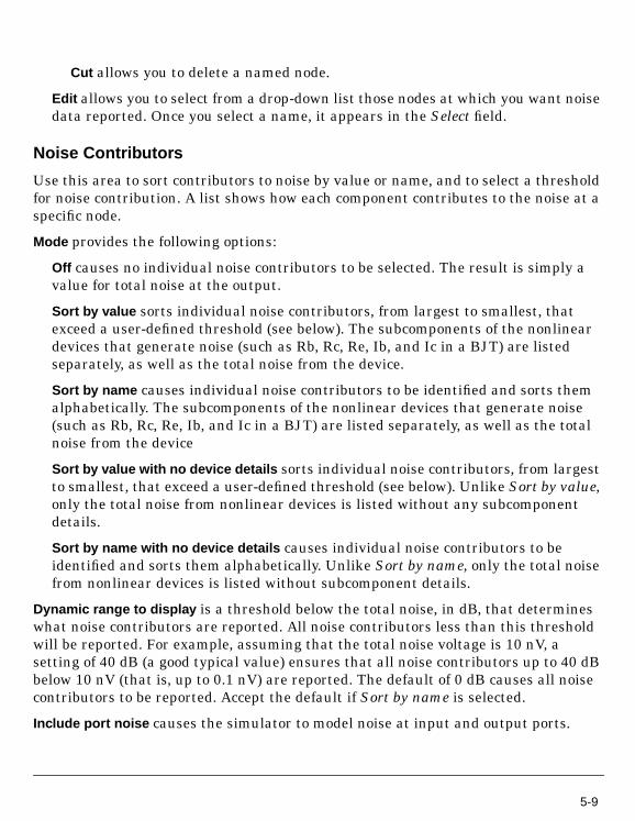
Cut allows you to delete a named node.
Edit allows you to select from a drop-down list those nodes at which you want noisedata reported. Once you select a name, it appears in the Select field.
Noise Contributors
Use this area to sort contributors to noise by value or name, and to select a thresholdfor noise contribution. A list shows how each component contributes to the noise at aspecific node.
Mode provides the following options:
Off causes no individual noise contributors to be selected. The result is simply avalue for total noise at the output.
Sort by value sorts individual noise contributors, from largest to smallest, thatexceed a user-defined threshold (see below). The subcomponents of the nonlineardevices that generate noise (such as Rb, Rc, Re, Ib, and Ic in a BJT) are listedseparately, as well as the total noise from the device.
Sort by name causes individual noise contributors to be identified and sorts themalphabetically. The subcomponents of the nonlinear devices that generate noise(such as Rb, Rc, Re, Ib, and Ic in a BJT) are listed separately, as well as the totalnoise from the device
Sort by value with no device details sorts individual noise contributors, from largestto smallest, that exceed a user-defined threshold (see below). Unlike Sort by value,only the total noise from nonlinear devices is listed without any subcomponentdetails.
Sort by name with no device details causes individual noise contributors to beidentified and sorts them alphabetically. Unlike Sort by name, only the total noisefrom nonlinear devices is listed without subcomponent details.
Dynamic range to display is a threshold below the total noise, in dB, that determineswhat noise contributors are reported. All noise contributors less than this thresholdwill be reported. For example, assuming that the total noise voltage is 10 nV, asetting of 40 dB (a good typical value) ensures that all noise contributors up to 40 dBbelow 10 nV (that is, up to 0.1 nV) are reported. The default of 0 dB causes all noisecontributors to be reported. Accept the default if Sort by name is selected.
Include port noise causes the simulator to model noise at input and output ports.
5-9
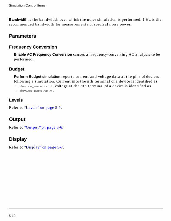
Simulation Control Items
Bandwidth is the bandwidth over which the noise simulation is performed. 1 Hz is therecommended bandwidth for measurements of spectral noise power.
Parameters
Frequency Conversion
Enable AC Frequency Conversion causes a frequency-converting AC analysis to beperformed.
Budget
Perform Budget simulation reports current and voltage data at the pins of devicesfollowing a simulation. Current into the nth terminal of a device is identified as...device_name.tn.i . Voltage at the nth terminal of a device is identified as...device_name.tn.v.
Levels
Refer to “Levels” on page 5-5.
Output
Refer to “Output” on page 5-6.
Display
Refer to “Display” on page 5-7.
5-10

Simulation Parameters: S_ParamThe tabs in the S_Param dialog box allow you to set the following parameters:
• Frequency sets parameters related to swept frequencies.
• Parameters allows S-, Y-, or Z-parameters to be selected, as well as group delay.It allows status and device operating point levels to be determined.It alsoprovides an option to output solutions at all steps.
• Noise calculates linear noise.
• Output allows you to selectively save your simulation data to a dataset.
• Display shows or hides parameters in the Schematic window.
The available parameters and options are described in the following sections.
Frequency
Sweep Type
Refer to “Sweep Type” on page 5-2.
Use Sweep Plan
Refer to “Use Sweep Plan” on page 5-2.
Parameters
Calculate
S-parameters causes S-parameters to be calculated.
Y-parameters converts the results of an S-parameter simulation to Y-parameters. TheS-parameters are also output.
Z-parameters converts the results of an S-parameter simulation to Z-parameters. TheS-parameters are also output.
Group delay causes a group delay simulation to be calculated from the S-parameterdata.
5-11

Simulation Control Items
Group delay aperture is the frequency aperture (as a percentage of actual frequency)over which is calculated.
Frequency Conversion
Check Enable AC frequency conversion to enable AC frequency. For S-parameterfrequency conv. point, add a numeric value to enable S-parameter frequency.
Levels
Refer to “Levels” on page 5-5.
Noise
Calculate noise causes a linear noise simulation to be performed. This option must beselected for the remaining noise options to be available.
Noise input port and Noise output port are used to get the noisy two-port parameters(NFmin, Sopt and Rn) when there are more than two Term (termination) componentson the schematic. Set Noise input port to the number specified by the Num parameteron the Term that is considered the input termination, and Noise output port to thenumber for the output termination. For two-port networks or when the noisy two-portparameters are not required, these can be left blank.
Noise contributors
Mode provides the following options:
Off causes no individual noise contributors to be selected. The result is simply avalue for total noise at the output.
Sort by value sorts individual noise contributors, from largest to smallest, thatexceed a user-defined threshold (see below). The subcomponents of the nonlineardevices that generate noise (such as Rb, Rc, Re, Ib, and Ic in a BJT) are listedseparately, as well as the total noise from the device.
Sort by name causes individual noise contributors to be identified and sorts themalphabetically. The subcomponents of the nonlinear devices that generate noise(such as Rb, Rc, Re, Ib, and Ic in a BJT) are listed separately, as well as the totalnoise from the device
Sort by value with no device details sorts individual noise contributors, from largestto smallest, that exceed a user-defined threshold (see below). Unlike Sort by value,
dΦ dω⁄
5-12

only the total noise from nonlinear devices is listed without any subcomponentdetails.
Sort by name with no device details causes individual noise contributors to beidentified and sorts them alphabetically. Unlike Sort by name, only the total noisefrom nonlinear devices is listed without subcomponent details.
Dynamic range to display is the range, in dB, over which the noise analysis isperformed. This applies only when noise contributors are selected.
Bandwidth is the bandwidth over which the linear noise simulation is performed. 1 Hzis the recommended bandwidth for measurements of spectral noise power
Output
Refer to “Output” on page 5-6.
Display
Refer to “Display” on page 5-7.
5-13
Simulation Control Items
Simulation Parameters: HBThe tabs in the Harmonic Balance dialog box allow you to set the followingparameters:
• Freq sets parameters related to the frequencies of fundamentals.
• Sweep sets parameters related to sweeps, and references sweep plans.
• Params sets status and device operating point levels, as well as parametersrelated to FFT oversampling and convergence.
• Small-Sig sets parameters related to small-signal/large-signal simulation.
• Noise (1) sets parameters related to noise simulation, including sweeps. Inputand output ports can be defined here. FM noise can be selected for oscillatorsimulations.
• Noise (2) selects nodes at which to calculate noise data, and sorts the noisecontributors. Port noise options are provided here also.
• NoiseCons is used to specify which NoiseCon nonlinear noise controllers shouldbe simulated, allowing more flexible noise simulations to be performed thanNoise(1) and Noise(2) allow.
• Osc sets parameters related to oscillator simulation.
• Solver allows you to choose between a Direct or Krylov solver or to enable anautomatic selection.
• Output allows you to selectively save your simulation data to a dataset.
• Display shows or hides parameters in the Schematic window.
The available parameters and options are described in the following sections.
Nodes for Calculation of Noise Parameters
Use this area to select nodes at which you want linear noise data to be reported.Noise voltages and currents are reported in rms units.
5-14

Freq
Fundamental Frequencies
Maximum order is the maximum order of the intermodulation terms in the simulation.For example, assume there are two fundamentals and Order (see below) is 3. IfMaximum order is 0 or 1, no mixing products are simulated. The frequency listconsists of the fundamental and the first, second, and third harmonics of each source.If Maximum order is 2, the sum and difference frequencies are added to the list. IfMaximum order is 3, the second harmonic of one source can mix with thefundamental of the others, and so on. The combined order is the sum of the individualfrequency orders that are added or subtracted to make up the frequency list.
Frequency is the frequency of the fundamental(s).
Order is the maximum order (harmonic number) of the fundamental(s) that will beconsidered.
Select edits the fundamental frequencies and their orders (by double-clicking).
Add adds a frequency and its associated fundamental and order.
Cut deletes a frequency and its associated fundamental and order.
Paste takes a frequency item that has been cut and places it in a different order inthe Select window.
Sweep
Refer to “Sweep” on page 5-2.
Params
Budget
Perform Budget simulation reports current and voltage data into and out of devicesfollowing a simulation. Current into a device is identified as ...device_name.t1.i ,and out of that device as ...device_name.t2.i . Voltage at the input to a device isidentified as ...device_name.t1.v , and at the output of that device as...device_name.t2.v .
5-15

Simulation Control Items
Levels
Refer to “Levels” on page 5-5.
FFT
Oversample sets the FFT oversampling ratio. Higher levels increase the accuracy ofthe solution by reducing the FFT aliasing error and improving convergence. Memoryand speed are affected less when the direct harmonic balance method is used thanwhen the Krylov option is used.
More brings up a small dialog box. To increase simulation accuracy, enter in the fieldan integer representing a ratio by which the simulator will oversample eachfundamental.
Convergence
Auto mode automatically adjusts key convergence parameters and resimulates toachieve convergence. As it trades efficiency for ease of use, it is suited to beginningADS users who are unfamiliar with the ADS parameters to control the convergence.
Manual mode enables an advanced damped Newton solver. This solver guarantees arobust and steady march toward the solution with each harmonic balance iteration.The convergence rate is enhanced by its selection of a near-optimal dampingconstant, choice of several individual norms in the convergence checks, and controlover the residual reduction threshold at each iteration.
Max. iterations is the maximum number of iterations to be performed. The simulationwill iterate until it converges, an error occurs, or this limit is reached.
Restart instructs the simulator not to use the last solution as the initial guess for thenext solution.
Use Initial Guess (Harmonic Balance)
Check this box to save your initial guess to a dataset that can be referred to for asubsequent harmonic balance simulation, including circuit envelope.For example, ifyou have saved the HB solution, you can later do a nonlinear noise simulation anduse this saved solution as the initial guess, removing the time required to recomputethe nonlinear HB solution. Or you could quickly get to the initial HB solution, andthen sweep a parameter to see the changes. In this later case, you will probablyeither want to disable the Write Final Solution (see following topic), or use a differentfile for the final solution, to avoid over-writing the initial guess solution. If no file
5-16
name is supplied, a default name is generated internally, using the design name andappending the suffix .hbs. A suffix is neither required nor added to any user suppliedfile name.
The Annotate value specified in the DC Solutions tab in the Options block is alsoused to control the amount of annotation generated when there are topology changesdetected during the reading of the initial guess file. Refer to the section “DCSolutions” on page 5-50. Since HB simulations also utilize the DC solution, to getoptimum speed-up, both the DC solution and the HB solution should be saved andre-used as initial guesses.
The initial guess file does not need to contain all the HB frequencies. For example,one could do a one-tone simulation with just a very nonlinear LO, save that solutionaway and then use it as an initial guess in a two tone simulation. The exactfrequencies do not have to match between the present analysis and the initial guesssolution. However, the fundamental indexes should match. For example, a solutionsaved from a two tone analysis with Freq[1] = 1GHz and Freq[2] = 1kHz would not bea good match for a simulation with Freq[1] = 1kHz and Freq[2] = 1 GHz.
If the simulator cannot converge with the supplied initial guess, it then attempts to aglobal node-setting by connecting every node through a small resistor to anequivalent source. It then attempts to sweep this resistor value to a very large valueand eventually tries to remove it.
Final Solution (Harmonic Balance)
Check this box to save your final HB solution to the output file. If a filename is notsupplied, a file name is internally generate using the design name, followed by an.hbs suffix. If a file name is supplied, the suffix is neither appended nor required. Ifthis box is checked, then the last HB solution is put out to the specified file. If this isthe same file as that used for the Initial Guess, this file is updated with the latestsolution.
Transient simulations can also be programmed to generate a harmonic balancesolution that can then be used as an initial guess for an HB simulation. Refer to thesection, “Compute HB Solution” on page 5-46.
5-17
Simulation Control Items
Small-Sig
This feature employs a large-signal/small-signal method to achieve much fastersimulations when some signal sources (a) are much smaller than others, and (b) canbe assumed not to exercise circuit nonlinearities. For example, in a mixer the LO tonecould be considered the large-signal source and the RF the small-signal source.
To edit these parameters and request a small-signal analysis, click Small-signal at thebottom of the dialog box.
Small-signal frequency
Refer to “Sweep” on page 5-2.
Use all small-signal frequencies solves for all small-signal mixer frequencies in bothsidebands. This default option requires more memory and simulation time, but isrequired for the most accurate simulations.
Merge small- and large-signal frequencies By default, the simulator reports only thesmall-signal upper and lower sideband frequencies in a mixer or oscillatorsimulation. Selecting this option causes the fundamental frequencies to be restoredto the dataset, and merges them sequentially.
Noise (1)
To edit these parameters and request a noise analysis, click Nonlinear noise at thebottom of the dialog box.
Noise frequency
Use this area to select the frequency(s) at which nonlinear noise is computed.
Sweep Type
Refer to “Sweep Type” on page 5-2.
Input Frequency
Because the simulator uses a single-sideband definition of noise figure, the correctinput sideband frequency must be specified here. This parameter identifies whichinput frequency will mix to the noise frequency of interest.
5-18

In the case of mixers, Input frequency is typically determined by an equation thatinvolves the local oscillator (LO) frequency and the noise frequency. Either the sum ofor difference between these two values is used, depending on whether upconversionor downconversion is taking place.
The above parameters do not need to be specified if only the output noise voltage isdesired (that is, if no noise figure is computed).
Noise input port is the number of the source port at which noise is injected. This iscommonly the RF port. Although any valid port number can be used, the output portnumber is frequently defined as Num=1.
Noise output port is the number of the Term component at which noise is retrieved.This is commonly the IF port. Although any valid port number can be used, the inputport number is frequently defined as Num=2.
Include FM noise (osc. only) causes an FM noise analysis to be performed in additionto a mixing noise analysis for oscillator phase noise. This simulates a second modelfor phase noise, which may be more accurate at small offset frequencies.
Noise (2)
To edit these parameters and request a noise analysis, click Nonlinear noise at thebottom of the dialog box.
Nodes for noise parameter calculation
Use this area to select named nodes at which the simulator will compute noise.
Note The fewer the number of nodes requested, the quicker the simulation and theless memory required.
Edit selects the named node(s) for the simulator to consider.
Select holds the names of the nodes the simulator will consider.
Add adds a named node.
Cut deletes a named node.
Paste takes a named node that has been cut and places it in a different order in theSelect window.
Simulation Parameters: HB 5-19
Simulation Control Items
Noise Contributors
Use this area to sort contributions to noise, as well as a threshold below which noisewill not be reported.
Mode provides the following options:
Off causes no individual noise contributors (nodes) to be selected. The result issimply a value for total noise at the node.
Sort by value sorts individual noise contributors, from largest to smallest, thatexceed a user-defined threshold (see below). The subcomponents of the nonlineardevices that generate noise (such as Rb, Rc, Re, Ib, and Ic in a BJT) are listedseparately, as well as the total noise from the device.
Sort by name causes individual noise contributors to be identified and sorts themalphabetically. The subcomponents of the nonlinear devices that generate noise(such as Rb, Rc, Re, Ib, and Ic in a BJT) are listed separately, as well as the totalnoise from the device
Sort by value with no device details sorts individual noise contributors, from largestto smallest, that exceed a user-defined threshold (see below). Unlike Sort by value,only the total noise from nonlinear devices is listed without any subcomponentdetails.
Sort by name with no device details causes individual noise contributors to beidentified and sorts them alphabetically. Unlike Sort by name, only the total noisefrom nonlinear devices is listed without subcomponent details.
Dynamic range to display is a threshold below the total noise, in dB, that determineswhat noise contributors are reported. All noise contributors more than this thresholdwill be reported. For example, assuming that the total noise voltage is 10 nV, asetting of 40 dB (a good typical value) ensures that all noise contributors up to 40 dBbelow 10 nV (that is, above 0.1 nV) are reported. The default of 0 dB causes all noisecontributors to be reported. Accept the default if Sort by name is selected.
Include port noise causes port noise to be included in noise currents and voltages.Ports must be placed and defined.
Calculate noisy two-port parameters causes an S-parameter simulation to beperformed. Ports must be placed and defined. The Noise input port parameter shouldbe set equal to the port number specified by the Num parameter on the input source,and the Noise output parameter to the number of the output Term (termination)component to Num=2. The following two-port parameters (dataset variables) arethen returned and can be plotted:
5-20 Simulation Parameters: HB

NFmin is the minimum noise figure of a two-port circuit. It is equal to the noisefigure when the optimum source admittance is connected to the circuit. (Its defaultunit is dB).
Sopt is the optimum source match for a two-port circuit. It is the reflectioncoefficient (looking into the source) that gives the minimum noise figure.
Rn is the effective noise resistance in ohms (unnormalized) of a two-port circuit.Effective noise resistance can be used to plot noise-figure circles or relatedquantities. This parameter determines how rapidly the minimum noise figuredeteriorates when the source impedance is not at its optimum value.
Icor is the noise current correlation matrix, in units of Amperes squared. Itdescribes the short circuit noise currents squared at each port, and the correlationbetween noise currents at different ports.
These expressions for noise simulation can be manipulated in equations.
Use all small-signal frequencies causes the simulator to solve for all small-signalmixer sidebands. This default option requires more memory but delivers moreaccurate results. In addition, it may require large kernel swap-size parameters. Onlyif there is insufficient memory should this option be set to no. Setting this option tono, causes only half of the small-signal mixer sidebands to be used and also usesone-fourth of the memory, but at the cost of generating potentially inaccurate results.Exercise caution when setting this option to no.
Note If you find you are running out of RAM, either set this parameter to no afterreading the paragraph above, or switch to the Krylov option.
Bandwidth is the bandwidth for spectral noise simulation. 1 Hz is the recommendedbandwidth for measurements of spectral noise power.
NoiseCons
This is used to select which NoiseCon nonlinear noise controllers should be simulatedwith the current harmonic balance analysis. These noise simulations will beperformed in addition to any noise simulation that may be set up with the Noise(1)and Noise(2) tabs.
Simulation Parameters: HB 5-21

Simulation Control Items
Note It is not necessary to enable Nonlinear Noise at the bottom of the dialog box inorder to select and simulate noise using NoiseCons. The Nonlinear Noise button isonly used with the Noise(1) and Noise(2) tabs.
The NoiseCons button must be clicked to enable noise simulation with NoiseCons.This button can be used to disable noise simulation of all NoiseCons without deletingthem from the Select NoiseCons list.
Edit is used to specify the name of the NoiseCon item to add to the simulation list.
Select NoiseCons holds the names of the NoiseCon items to be simulated.
Add adds a NoiseCon name.
Cut deletes a NoiseCon name.
Paste takes a NoiseCon name that has been cut and places it in a different order inthe Select window.
Osc
To enter the name of an oscillator port and request an oscillator analysis, clickOscillator at the bottom of the dialog box. An OscPort component is required.)
Oscport name is the name of the OscPort analysis component. The circuit simulator isalso capable of automatically finding the OscPort or OscPort2 component if the nameis set to “yes ”. Setting the name to “yes ” is required if the OscPort2 component is usedand should work unless there are two or more OscPorts in the circuit, which isneither useful nor recommended.
Solver
The Solver tab allows you to select from two separate harmonic balance techniques,or to allow the simulator to assign one automatically.
Direct Solver is best suited for smaller problems and is faster.
Krylov Solver , intended for larger problems, includes advanced preconditioningtechnology with an iterative linear solver. This method greatly reduces memoryrequirements in large harmonic balance problems, such as those encountered inRFICs or RF System simulations.
5-22 Simulation Parameters: HB
Auto Select allows the simulator to choose which solver would be most effective forthe active design.
Optional Auto Select Info
Estimated available RAM in MB . Enter the value, if desired, to specify the memoryavailable to the simulator. This depends not only on the overall RAM, but also on theway the specific machine is used, in particular on the memory used by otherprocesses. The default value is set conservatively to 128.
Krylov Parameters
Matrix packing directs the solver to use the technique known as spectral packing,which reduces the memory needed for the Jacobian, typically by 60-80%. The penaltyis a longer computation time if no swapping is required. By default, this feature isturned off. You should turn on for extremely large problems in which the availableRAM would not be able to accommodate the Jacobian.
Maximum number of iterations is the maximum number of GMRES iterations allowed.It is used to interrupt an otherwise infinite, loop in the case of poor or no convergence.The default is intentionally set to a large value of 150 to accommodate even slowlyconvergent iterations. You can still increase this number in cases where poorconvergence may be improved and you are willing to allow more time for it.
GMRES restart length sets the number of GMRES iterations before the solver restarts.At this point the algorithm does not need data from previous steps, and thecorresponding memory is released. Thus smaller values lead to lower memoryrequirements, but might significantly affect convergence. The default is 10, and it isstrongly recommended that you avoid decreasing this value unless the problem isextremely large and convergence is carefully monitored. Larger values offerpotentially more robust performance, but require more memory.
Krylov noise tolerance sets the tolerance for the Krylov solver when that solver is usedeither for small-signal harmonic balance analysis or for nonlinear noise analysis. Itneeds to be tight, and the default value is 1e-10. Larger values may lead to lessaccurate results, while further tightening may require longer simulation times.
Preconditioner
The Krylov solver requires a preconditioner for robust and efficient convergence. Thefollowing options are offered:
Simulation Parameters: HB 5-23

Simulation Control Items
• Auto allows the simulator to choose which preconditioner would be mosteffective for the active design.
• DCP is the default preconditioner, which is effective in most cases, but fails forsome very strong nonlinear circuits. It uses a DC approximation on the entirecircuit. Due to its block-diagonal nature, it can be factored once and appliedinexpensively at each linear solve step.
• BSP is recommended for instances when a Krylov HB simulation fails toconverge using the DCP option. The BSP preconditioner typically ensuresrobust convergence on even the most highly nonlinear circuits. On those circuitsthat converge with DCP, the overhead that the BSP preconditioner introducesis minimal. On circuits that fail with the DCP, using the BSP option willproduce convergence at the cost of additional memory usage.
• SCP (Schur-Complement) is intended for use with those circuits that fail toconverge with the DCP preconditioner. The approximation partially excludesthe most nonlinear parts. The sequence of steps is much more complex thanwith DCP, including an internal Krylov loop. It can also be more expensive,particularly in memory usage.
Waveform Memory Reduction
Use dynamic waveform recalculation enables reuse of dynamic waveform memoryinstead of upfront strorage on all waveforms. Small circuits might simulate a littleslower, but not significantly.
Use compact frequency map enables a spectral compression, typically requiring lessmemory for individual waveforms.
Output
Refer to “Output” on page 5-6.
Display
Use the following options to show or hide all available parameters for a simulation:
Display parameter on schematic is a field that allows you to select those parametersto be made visible ion the schematic.
Set All shows all parameters.
5-24 Simulation Parameters: HB
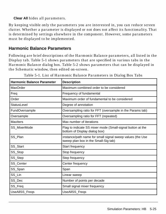
Clear All hides all parameters.
By keeping visible only the parameters you are interested in, you can reduce screenclutter. Whether a parameter is displayed or not does not affect its functionality. Thatis determined by settings elsewhere in the component. However, some parametersmust be displayed to be implemented.
Harmonic Balance Parameters
Following are brief descriptions of the Harmonic Balance parameters, all listed in theDisplay tab. Table 5-1 shows parameters that are specified in various tabs in theHarmonic Balance dialog box. Table 5-2 shows parameters that can be displayed inthe Schematic window, then edited on-screen.
Table 5-1. List of Harmonic Balance Parameters in Dialog Box Tabs
Harmonic Balance Parameter Description
MaxOrder Maximum combined order to be considered
Freq Frequency of fundamental
Order Maximum order of fundamental to be considered
StatusLevel Degree of annotation
FundOversample Oversampling ratio for FFT (oversample in the Params tab)
Oversample Oversampling ratio for FFT (repeated)
MaxIters Max number of iterations
SS_MixerMode Flag to indicate SS mixer mode (Small-signal button at thebottom of Display dialog box)
SS_Plan Instance/path name for small signal sweep values (the Usesweep plan box in the Small-Sig tab)
SS_Start Start frequency
SS_Stop Stop frequency
SS_Step Step frequency
SS_Center Center frequency
SS_Span Span
SS_Lin Linear sweep
SS_Dec Number of points per decade
SS_Freq Small signal mixer frequency
UseAllSS_Freqs UseAllSS_Freqs
Simulation Parameters: HB 5-25

Simulation Control Items
MergeSS_Freqs MergeSS_Freqs
InputFreq InputFreq
NLNoiseMode Flag to indicate nonlinear noise mode
NoiseFreqPlan Instance/path name for noise sweep values
NLNoiseStart Start frequency
NLNoiseStop Stop frequency
NLNoiseStep Step frequency
NLNoiseCenter Center frequency
NLNoiseSpan Span
NLNoiseLin Linear sweep
NLNoiseDec Number of points per decade
FreqForNoise Single point noise frequency
NoiseInputPort Input port for noise figure calculation
NoiseOutputPort Output port for noise figure calculation
PhaseNoise Specify noise frequency as offset from oscillation frequency
FM_Noise Consider AM to FM conversion in oscillator phase noise analysis
NoiseNode Nodename to compute noise voltage (repeatable)
SortNoise Sort Noise Contribution by: Value/1, Name/2 (default:0/NoOutput)
NoiseThresh Noise Contribution Threshold
IncludePortNoise Include port noise in noise voltage and currents
NoisyTwoPort Compute noisy two-port parameters: sopt, rn & nfmin
BandwidthForNoise Bandwidth for spectral noise analysis
OutputBudgetIV Output top-level pin currents and voltages
UseKrylov Output top-level pin currents and voltages
GMRES_Restart GMRES iterations before auto-restart
KrylovUsePacking Use Krylov spectral packing
KrylovMaxIters Maximum number of GMRES iterations
AvailableRAMsize RAM available to the simulator
KrylovSS_Tol Krylov tol. for small-sig spectral / noise analysis
Table 5-1. List of Harmonic Balance Parameters in Dialog Box Tabs
Harmonic Balance Parameter Description
5-26 Simulation Parameters: HB

RecalculateWaveforms Use dynamic waveform storage
UseCompactFreqMap Compress spectrum
OscMode Flag to indicate oscillator mode
OscPortName Oscillator port used to break feedback loop
SweepVar Name of variable or parameter to be swept
SweepPlan SweepPlan instance path name for sweep values
Start Start value
Stop Stop value
Step Step value”
Center Center value
Span Span
Lin Linear sweep
Dec Number of points per decade
Pt Single point
UseNodeNestLevel Use Node Nest Level
NodeNestLevel Node Nest Level
NodeName Node Name
UseEquationNestLevel Use EquationNest Level
EquationNestLevel Equation Nest Level
Equation Name Equation Name
DevOpPtLevel Levels of DC Operating Point Data to output
Noisecon Instance name for noise controller
NoiseConMode Flag to indicate NoiseCon mode
InFile File name for reading HB Initial Guess
UseInFile Read file prior to an HB solve
OutFile File name for writing HB Final Solution
UseOutFile Write last HB solution to file
KrylovPrec Flag to indicate Preconditioner
ConvMode Convergence Mode
OutputPlan Selective saving to dataset
Table 5-1. List of Harmonic Balance Parameters in Dialog Box Tabs
Harmonic Balance Parameter Description
Simulation Parameters: HB 5-27

Simulation Control Items
For additional information on setting up Harmonic Balance analysis, refer to thefollowing chapters in the Circuit Simulation documentation:
• Chapter 7, Harmonic Balance Simulation, for an overview
• Chapter 8, Harmonic Balance for Nonlinear Noise Simulation, describes how touse the simulator for calculating noise.
• Chapter 9, Harmonic Balance for Oscillator Simulation, describes how to usethe simulator with oscillator designs.
• Chapter 11, Harmonic Balance for Mixers, describes how to use the simulatorwith mixer designs.
Table 5-2. List of Additional Harmonic Balance Parameters
Harmonic Balance Parameter Description
PackFFT Pack FFT in multi-tone analysis
GuardThresh Guard threshold
SamanskiiConstant SamanskiiConstant
Restart Do not use last solution as initial guess
ArcLevelMaxStep Maximum arc-length step for source-level continuation
MaxStepRatio Ratio of maximum to given number of steps
MaxShrinkage Maximum step shrinkage
ArcMaxStep Maximum arc-length step
ArcMinValue Minimum value for parameter during arclength continuation
ArcMaxValue Maximum value for parameter during arclength continuation
SS_Thresh Small signal spectral threshold”
KrylovPackingThresh Krylov bandwidth threshold
KrylovTightTol GMRES tolerance
KrylovLooseTol Loose tolerance for Krylov loop
KrylovLooseIters KrylovLooseTol
KrylovLooseIters KrylovLooseIters
KrylovUseGMRES_Float Min number of iterations to invoke loose tolerance
IgnoreOscErrors Continue sweep even after oscillation convergence error
Other Output string to netlist
5-28 Simulation Parameters: HB
Simulation Parameters: LSSPThe parameters for the LSSP Simulation component are identical to those for HB,with two exceptions:
• This simulation component has a Ports tab.
• The options for Small-signal mode, Nonlinear noise, and Oscillator are notavailable.
Refer to the section “Simulation Parameters: HB” on page 5-14.
The Ports parameters are described below.
Ports
Port Frequency
Ports must be placed and defined. Set the port number of the input source to Num=1,and the port number of the output Term (termination) component to Num=2.
Use this area to edit the following parameters:
Select edits the following:
Port is the number of the port.
Frequency is the frequency of the port.
Add adds a port and its associated frequency.
Cut deletes a port and its associated frequency.
Edit edits the frequency of a selected port.
P2D SimulationFor information on the P2D component, refer to Chapter 14, P2D Simulation, in theCircuit Simulation documentation.
Simulation Parameters: LSSP 5-29

Simulation Control Items
Simulation Parameters: XDB
Freq
Refer to “Freq” on page 5-15.
X dB
Gain Compression
Enter the gain compression, the default is 1 dB.
Port numbers
Input is the number of the input port.
Output is the number of the output port.
Port frequencies
Input is the frequency at the input port.
Output is the frequency at the output port.
Power tolerances
Input is the variation in power, measured as a change in dB (delta dB), allowed at theinput port.
Output is the variation in power, measured as a change in dB (delta dB), allowed atthe input port.
Max. Input Power is the maximum input power (in dBm) allowed before the simulatoraborts. This setting is used to prevent the simulator from continuing to search if it ishaving difficulty finding a solution.
Params
Refer to “Params” on page 5-15.
5-30 Simulation Parameters: XDB

Solver
Refer to “Solver” on page 5-22.
Output
Refer to “Output” on page 5-6.
Display
Refer to “Display” on page 5-7.
Simulation Parameters: XDB 5-31
Simulation Control Items
Simulation Parameters: Circuit EnvelopeThe tabs in the Envelope dialog box allow you to set the following parameters andoptions:
• Env Setup sets parameters related to time and frequency.
• Env Params selects an integration mode and sweep offset, turns on source andresistor noise, and sets device-fitting parameters. Options for oscillator analysisare also available.
• HB Params sets parameters related to convergence, status and device operatingpoint levels, and FFT oversampling.
• Small-Sig sets parameters related to small-signal/large-signal simulation.
• Noise (1) sets parameters related to noise simulation, including sweeps. Inputand output ports can be defined here.
• Noise (2) selects nodes at which to calculate noise data, and sorts the noisecontributors. Port noise options are provided here also.
• Output allows you to selectively save your simulation data to a dataset.
• Display shows or hides parameters in the Schematic window.
The available parameters and options are described in the following sections.
Env Setup
Times
Use this area to edit the following parameters:
Stop time is the time the analysis stops.
Time step sets the fixed time step that the simulator uses to calculate thetime-varying envelopes.
Note The parameter Time step defines the maximum allowed bandwidth(±0.5 /Time step) of the modulation envelope. Because of the nature of thetime-domain integration algorithms, the analysis bandwidth (1/Time step) should beat least twice as large as the modulation bandwidth to achieve accurate simulationsat the maximum modulation frequencies. Stop time simply defines the maximumduration of the swept time simulation. An analysis starts at time = 0, so the total
5-32 Simulation Parameters: Circuit Envelope
number of simulation time points that are stored is equal to (Stop time)/Time step. Ateach time point, the envelope values of all of the analysis frequencies, including DC,are saved.
Fundamental Frequencies
Refer to “Fundamental Frequencies” on page 5-15.
Env Params
Env Params
This area allows you to select the following:
Integration provides the following integration options in a popup menu:
Backward Euler invokes the backward-Euler integration algorithm.
Trapezoidal invokes the trapezoidal integration algorithm.
Gear’s invokes Gear’s method.
Sweep offset disables data output until the time elapsed exceeds the value entered inthis field. It then subtracts the value in the field from the output time. Enterappropriate values in this field to eliminate undesired responses resulting fromturn-on transients.
Turn on all noise includes in the simulation the white noise in devices such asresistors, lossy transmission lines, diodes, transistors, etc. This adds independent,white, Gaussian noise at all of the envelope frequencies. Explicit noise sources, suchas V_Noise, I_NoiseBD, OSCwPhNoise Amplifier, etc., also add their noisecontribution. Full nonlinear circuit equations are applied to the resulting compositesignal, so that no small-signal assumptions have to be made about the relative size ofthe noise, and random times and voltages are added to the simulation. The noise willbe complex for non-baseband envelope frequencies, generating both amplitude- andphase-equivalent noise.
Device Fitting
There are several ways to control the linear device, time-domain modeling requiredby the circuit envelope simulator when analyzing a modulation envelope. Mostbuilt-in elements now have an Laplace or a transmission line approximation. This
Simulation Parameters: Circuit Envelope 5-33

Simulation Control Items
parameter is used only with respect to dataset devices or generic linear devices whosefrequency response cannot be represented as a rational polynomial of the form
where s is the Laplace variable, T is time delay, and P and Q are the numeratorand denominator polynomials, respectively.
For linear elements a model must be generated that reflects the envelope frequencyresponse around each of the analysis frequencies. The first three parameters in thisarea are used in a pole/zero fit of the frequency response around each carrierfrequency. The remaining options are used when a valid or sufficiently accuratepole/zero fit cannot be obtained.
Bandwidth fraction determines what fraction of the envelope bandwidth to use todetermine the fit.
Note The default value for Bandwidth fraction is 1, so that only the frequencyvalues within ±0.1/Time step of the center carrier frequency are used to determine thefit. If greater accuracy is required at the edges of the envelope bandwidth, thisnumber can be increased. However, the simulator will then typically require a higherorder and a more time-consuming fit to be generated and then used during thesimulation. Also, the integration algorithms cannot maintain 100% percent accuracyout to the edges of the envelope bandwidth. Note that a Bandwidth fraction value of0.0 will effectively disable this pole/zero fitting, and just the constant value will beused. This will result in the fastest simulation, but any transient effects from thesemodels will not be included. The Relative tolerance and Absolute toleranceparameters (see below) can also be set to help determine how accurate a fit is desired.
Relative tolerance sets a relative truncation factor for envelope fitting.
Absolute tolerance sets an absolute truncation factor for envelope fitting.
Warn when poor fit causes a warning message to appear when an envelope fit is poor.
Use fit when poor instructs the simulator to use poor fits instead of constant values.
Skip fit at baseband instructs the simulator not to use pole/zero fitting at the baseband(DC) envelope.
sT–eP s( )Q s( )------------
5-34 Simulation Parameters: Circuit Envelope
Note If an external frequency-domain-device is supplied (such as an n-port datadevice using a dataset of S-parameter measurements read from an instrument), andthat device does not accurately represent the low-frequency or DC response, then agood pole/zero fit may not be obtained. Three of the above parameters determinewhat to do in these cases. Skip fit at baseband can be used to disable the fittingprocess at just the DC (baseband) frequencies. Warn when poor fit can be used todisable the output of these warnings. Use fit when poor then determines whether touse these poor fits in the simulation or to replace them with the constant, centerfrequency value. However, there is a potential risk associated with using poor fits, inthat the simulation may generate incorrect, possibly unstable results.
Oscillator Options
This area allows you to select the following options specific to oscillator simulation:
Use OscPort causes a normal harmonic balance simulation to be performed prior tothe first time step. This is used to determine and set the analysis frequency to thesteady-state oscillator frequency. Select this option to enter an Oscport name.
Note If the oscillation frequency does not change significantly during its buildup,this option often allows larger time steps to be used. This is because the envelopebandwidth does not have to include any uncertainty as to the oscillator’s finalfrequency.
Oscport name is the name of the OscPort component. You must select Use OscPortto enter a name.
Calculate oscillator start-up transient is available only when an Oscport name isentered. This option resets the oscillator voltage solution to zero so that thetransient buildup can be simulated. If this option is not selected, the time-domainsolution begins at the steady-state solution, the transient buildup time is skipped,and the oscillator can immediately start responding properly to any externalmodulation.
Note The OscPort component is used only for this initial simulation. It is disabledonce the actual envelope simulation starts.
HB Params
Convergence
Refer to “Convergence” on page 5-16.
Simulation Parameters: Circuit Envelope 5-35

Simulation Control Items
Levels
Refer to “Levels” on page 5-5.
Note To view a report of the simulator’s progress in the Status/Summary windowwhile the simulation is running, set Status level to 3.
FFT
Refer to “FFT” on page 5-16.
Use Initial Guess
Refer to the section “Use Initial Guess (Harmonic Balance)” on page 5-16.
Final Solution
Refer to the section “Final Solution (Harmonic Balance)” on page 5-17.
Small-Sig
Refer to “Small-Sig” on page 5-18.
Noise(1)
Refer to “Noise (1)” on page 5-18. These parameters enable you to set up and run asmall-signal/Harmonic Balance noise analysis following the final time point of thesimulation. However, FM noise will not be performed.
Noise(2)
Refer to “Noise (2)” on page 5-19.
Output
Refer to “Output” on page 5-6.
Display
Refer to “Display” on page 5-7.
5-36 Simulation Parameters: Circuit Envelope
Simulation Parameters: TranThe tabs in the Tran dialog box allow you to set the following parameters:
• Time Setup sets start and stop time and the size of time steps.
• Integration determines truncation and integration techniques, as well as chargeaccuracy.
• Convolution sets parameters related to generating impulse responses forconvolution analysis.
• Convergence sets a variety of parameters to improve convergence.
• Options sets annotation and device operating point levels. It also provides anoption to output solutions at all steps.
• Noise sets the parameters for the generation of pseudorandom noise at eachtimestep.
• Freq sets the frequency of each fundamental frequency.
• Output allows you to selectively save your simulation data to a dataset.
• Display shows or hides parameters in the Schematic window.
The available parameters and options are described in the following sections.
Time Setup
Output Times
Start time is the time at which the simulator begins outputting time-point results.
Stop time is the time at which the simulator stops outputting time-point results.This parameter must be specified by the user.
Max time step is the largest time step to be taken in the simulation. This parametermust be specified by the user.
Min time step is the smallest time step to be taken in the simulation. Generally thedefault value is satisfactory.
Limit timestep for Transmission Line Where transmission lines are involved, thisfurther limits the time step to half of the shortest transmission line’s delay time.
Simulation Parameters: Tran 5-37

Simulation Control Items
Integration
Time step control method
This popup menu provides the following options:
Fixed selects a fixed time-step method. The simulation is performed with auniform, constant time step that is specified by Max time step (under the TimeSetup tab). It is quicker than the other methods. However, it is not as robust,because it cannot select a smaller time step when convergence problems areencountered.
Iteration count uses the number of Newton-Raphson iterations that were needed toconverge at a time point as a measure of the rate of change of the circuit. If thenumber of iterations is less than an internal threshold, the time step is doubled; ifthe number is greater than Max iterations per time step, the time step is scaled bya factor of Integration coefficient mu divided by 8 (see below). This method has aminimal computational overhead, but does not take into account the true rate ofchange of circuit variables.
Trunc Error is the default method for transient analysis. Trunc Error uses thecurrent estimate of local truncation error to determine an appropriate time step.Although it takes longer than Iteration count, it sets a meaningful error bound oncomputed output values.
Local truncation error over-est factor is a value against which the simulation’s errortolerance is compared. In transient analysis each time step is computed by means ofthe truncation-error estimate method. If the error is within acceptable limits, theresults are stored and analysis continues at the next time point. Otherwise, theanalysis is repeated at a smaller time step.
Charge accuracy determines the charge tolerance used in computing the localtruncation error.
5-38 Simulation Parameters: Tran
Integration
Use this area to select and define an integration method:
Trapezoidal integrates between time points by assuming they are connected by linesegments. The local truncation error is then related to the difference between theareas determined by the present and previous time points.
Gear’s integrates by assuming that the time points are connected by a polynomialcurve. The order of the polynomial is controlled by the Max Gear order parameter(see below). Lower-order polynomials tend to create greater truncation error, whilehigher-order polynomials can become unstable.
Max Gear order determines the maximum order of the polynomial when Gear’smethod is used. The default is 2. This is available only when Gear’s is selected (seeabove).
Integration coefficient mu is a coefficient that determines the degree of mixing ofthe trapezoidal (mu = 0.5) and backward-Euler (mu = 0.0) methods when thetrapezoidal method is used. This is available only when Trapezoidal is selected(see above).
The integration order at each timestep is output to the dataset as the variabletranorder. This data is used by the fs() function in the data display server to doaccurate interpolation of the data when an FFT is required. For the defaulttrapezoidal integration, this will normally have a value of 2, except atsource-induced breakpoints where it will be 1.
Simulation Parameters: Tran 5-39
Simulation Control Items
Convolution
Use approximate models when available causes the simulator to bypass impulse-basedconvolution (when that option is available to the user). Instead, it uses models that,although somewhat less accurate, can provide faster simulations. Theseapproximations neglect effects such as frequency-dependent loss and dispersion, butinclude the basic delay and impedance. These models are the default, if noconvolution license is available.
Approximate short transmission lines specifies a limit on the time delay below whichtransmission lines will be approximated instead of modeled as a delay line. Thisallows the user to analyze very short transmission lines with a Laplace transformapproximation. Also, it does not require the simulator to take the very small timesteps normally associated with short transmission lines. Only single, two terminal,transmission lines (like MLIN and TLIN, but not MCLIN and TLIN4) can beapproximated this way.
Max Frequency is the maximum frequency to which a frequency-domain device isevaluated to obtain its impulse response. By default, the program chooses this valueiteratively and separately for each device, in order to obtain a good impulse response.The user does not normally need to set this, unless it is necessary to prevent devicesfrom being evaluated in an invalid region.
Note With the exception of Max Frequency, it is recommended that the remainingparameters under this tab be left at their default settings and edited only in specialcases.
Delta frequency is the frequency interval between samples in the evaluation offrequency-domain-defined devices.
Max impulse sample points is the maximum number of points allowed in an impulseresponse.
Relative impulse truncation factor is the relative truncation factor for the impulseresponse.
Absolute impulse truncation factor is the absolute truncation factor for the impulseresponse.
Convolution interpolation order is the interpolation order used during convolutionsimulation.
5-40 Simulation Parameters: Tran
Convolution mode
This popup menu provides the following options:
Discrete causes a periodic extension of the frequency response that is modeled fromDC to Max Frequency. This is many times faster than PWL Continuous (see below).
PWL Continuous always leads to a low-pass response. This may be desirable where alow-pass response is modeled.
Smoothing window type
This popup menu applies to time-domain impulse responses that are derived fromnoncausal frequency functions (such as Hilbert transforms, integrators, ordifferentiates). A smoothing window reduces ripple in the approximation caused bydiscontinuities in the frequency function. The window is a multiplier function that isapplied to data prior to their conversion (by means of an inverse Fourier transform)to an impulse response.
A significant advantage of a window is its ability to reduce the exaggerated effects ofnoise in high-dynamic-range systems, resulting in a more realistic noise floor. It isalso useful in the analysis of digital filters, by removing nonphysical artifacts andallowing a filter’s response to be viewed more realistically.
The popup menu provides the following options:
Rectangle applies a function that truncates both noncausal and trailing responses.
Hanning applies a function that is smoother than that provided by Rectangle.
Non-causal fcn imp response length determines the length of the impulse response fornon-causal impulse responses. The unit is the number of sampling points. Non-causalimpulse responses are caused by elements like ideal phase shifters. They aremodeled, but with an added delay based on this value.
Simulation Parameters: Tran 5-41
Simulation Control Items
Convergence
Use user-specified initial conditions instructs the simulator to use user-specified initialconditions to compute the initial charges and fluxes in the circuit. The simulator willskip time=0 dc analysis.
When this option is enabled, the simulator uses the currents specified in the InitCondfield of the inductors and the branch voltages specified in the InitCond field of thecapacitors, as well as the node voltages specified in both the Simulation-TransientInitCond and Simulation-Transient InitCondByName components to compute theinitial charges and fluxes in the circuit. The voltage given in the capacitor's InitCondfield will take precedence over the voltage given in the Simulation-TransientInitCond and Simulation-Transient InitCondByName components if there is aconflict.
When the option is disabled and the Simulation-Transient InitCond and/orSimulation-Transient InitCondByName components are placed on the schematic, thesimulator will start the transient analysis with a DC analysis at time=0 and try toforce those node voltages identified in the Simulation-Transient InitCond and/orSimulation-Transient InitCondByName components to be close to the voltagesspecified. The values, if any, given in the InitCond field of the capacitors andinductors, however, will not be used.
Connect all nodes to GND via GMIN during initial DC analysis is useful in conditionswhere open circuits would result in a singular matrix error (where the diagonal termis missing). When selected, this option instructs the simulator to insert a resistorvalued at 1e12 ohms between any node and ground, whether at the circuit or thedevice level. (“GMIN” stands for minimum conductance.) This allows the user to stillobtain useful results.
Perform KCL check for convergence checks to verify how closely Kirchoff ’s CurrentLaw is satisfied at each node. This also depends on how the current tolerances are set(under the Convergence tab of the Options component). This option is selected bydefault.
Check only delta voltage for convergence looks for only the voltage difference betweentwo consecutive iterations. This less-stringent check saves both time and memory.This option is selected by default.
Check for strange behavior at every timestep looks for inordinate device currents orvoltages and returns a warning message when it finds any for devices or modelswhich support the Overload Alert and have their limit values specified. Although thiscan be a little slower, it is useful where out-of-bounds conditions are suspected.
5-42 Simulation Parameters: Tran
Skip device evaluation if volt chg are small between iters instructs the simulator tobypass the full evaluation of a device if it finds small voltage changes betweeniterations. This can improve simulation time in digital circuits containing manydevices. What is a “small” voltage change is determined by how voltage tolerances areset (under the Convergence tab of the Options component).
Max iterations per time step is the maximum number of iterations allowed for eachtime step.
Max iterations @ initial DC is the maximum number of iterations allowed during DCanalysis, before the stepping of the source begins.
Setting Initial Conditions with InitCond Components
There are two elements for setting initial conditions in a transient simulationInitCond and InitCondbyName. InitCond and InitCondByName are used to providean initial DC value for transient analysis only. These elements attach the specifiedvoltage source with a series resistor to the specified node(s) to force a value. The DCsolution for the entire circuit is then calculated. This DC solution is then used as thestarting state for the transient analysis.
Simulation Parameters: Tran 5-43
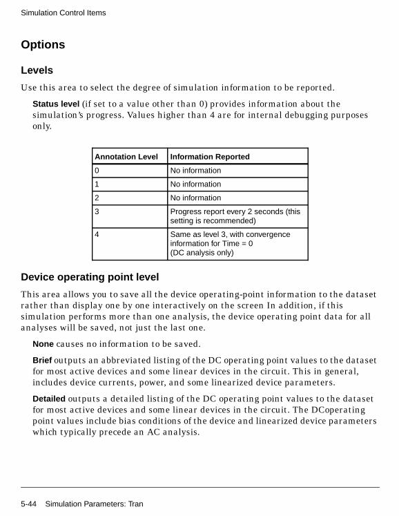
Simulation Control Items
Options
Levels
Use this area to select the degree of simulation information to be reported.
Status level (if set to a value other than 0) provides information about thesimulation’s progress. Values higher than 4 are for internal debugging purposesonly.
Device operating point level
This area allows you to save all the device operating-point information to the datasetrather than display one by one interactively on the screen In addition, if thissimulation performs more than one analysis, the device operating point data for allanalyses will be saved, not just the last one.
None causes no information to be saved.
Brief outputs an abbreviated listing of the DC operating point values to the datasetfor most active devices and some linear devices in the circuit. This in general,includes device currents, power, and some linearized device parameters.
Detailed outputs a detailed listing of the DC operating point values to the datasetfor most active devices and some linear devices in the circuit. The DCoperatingpoint values include bias conditions of the device and linearized device parameterswhich typically precede an AC analysis.
Annotation Level Information Reported
0 No information
1 No information
2 No information
3 Progress report every 2 seconds (thissetting is recommended)
4 Same as level 3, with convergenceinformation for Time = 0(DC analysis only)
5-44 Simulation Parameters: Tran

Output Solutions
Output All Internal Timepoints causes the simulator to save simulation results at allinternal timepoints; this option is on by default. Deselecting this option causesresults to be saved at least as often as the Max timestep option but some of theintermediate points will be suppressed. For simulations that take many smalltimesteps due to automatic timestep control, but whose output is stillwell-sampled at Max timestep, this can make the resulting datasets smaller andmake the post-processing of the data faster.
Noise
Noise bandwidth enables the generation of pseudorandom noise at each timestep.NoiseBandwidth controls the bandwidth of the generated noise and must be less than1/(2*MaxTimeStep). If this parameter is not specified or zero, no noise is generated.
Noise scale is a multiplicative scaling applied to all generated noise.
Simulation Parameters: Tran 5-45
Simulation Control Items
Freq
Edit
Frequency allows you to enter a fundamental frequency. You can edit it in theSelect field (see below).
Note These settings are used only for frequency sources whose frequency is notdefined explicitly. For example, V[1,0,–2] could be used to define a frequency that isFund1 – 2*Fund3.
Select
Use this field to copy (Add) or delete (Cut) fundamental frequencies.
Compute HB Solution
Transient simulations can also be programmed to generate a harmonic balancesolution that can then be used as an initial guess for an HB simulation. For example,in circuits such as dividers, HB cannot usually directly converge on a solution sincemultiple mathematical, but useless, solutions exist. By first running a Transientsimulation and generating an HB solution file and then using this as an initial guessfor an HB simulation, the HB simulation can then converge to the desired solution.
The Frequency values can still be used, independent of this HB solution mode, todefine the fundamental frequencies and _freqN variables used in sources. The Orderand Maximum order information is just used to determine the number of frequenciesfor which to compute an HB solution.
To enable the generation of the HB solution, the Write Solution box must be checked.A file name would also normally be provided, but as with the HB analysis, a defaultone will be generated if none is given.
To get the best results for the HB solution, it is generally recommended that theTransient analysis be run in fixed timestep control mode. Also, it's generally best,especially in multi-tone applications, to also check the Apply Window box. Thisapplies a Hanning window to the time domain data. To get a reasonable Fouriertransform, the duration of the Transient simulation must be longer than the period ofthe smallest specified frequency. A factor of 4 is often used here. It is also best tomake sure that the Transient simulation has reached an approximately steady state
5-46 Simulation Parameters: Tran

solution. This does not have to be precise, since this is just providing an initial guessvalue to the HB simulation. The start time of the Transient simulation can be used,in this compute HB solution mode, to indicate when this approximate steady statesolution has been reached. The internal Fourier transform will then not begin untilafter this start time.
Output
Refer to “Output” on page 5-6.
Display
Refer to “Display” on page 5-7.
Simulation Parameters: Tran 5-47
Simulation Control Items
Options ComponentThe Options component is available in all of the simulation control libraries to allowchanging settings for the simulation.
Misc
Simulation temperature models a temperature and temperature scale at which asimulation will be run. The default is 25 degrees Celsius.
Note The Options component is commonly used in nonlinear noise analyses. TheIEEE standard temperature (T0) for noise figure measurement is 290 K (16.85degrees Celsius). This can be set by editing Temp=16.85 in the Schematic window, orby selecting the Misc tab and editing Simulation temperature to that value.
Perform topology check performs a topology check before a simulation is run. This isthe default. Nodes that are leading to difficulty will be reported in theSimulation/Synthesis Messages window.
Use S-parameters when possible cause the simulator to attempt an S-parametersimulation on linear devices.
Maximum spectral size is the maximum number of mixing products considered in aharmonic balance simulation.
Convergence
Use the parameters below to select DC convergence options, as well as voltage andcurrent convergence criteria (tolerances).
DC Convergence
Use this area to select Max. delta voltage (“Max. delta V”) and Mode (convergencemode). Refer to “Parameters” on page 1-3 for a detailed discussion of this and otherDC parameters.
Convergence Check
There are three tolerance presets to provide options for beginning users.
5-48 Options Component

Relaxed yields fast but less accurate simulations. It is intended for use in the initialstages of the circuit design process or for quick simulation estimates.
Intermediate offers a middle ground between Relaxed and Strict.
Strict yields the most accurate results, but is the slowest. This is the default.
Tolerances
Voltage relative tolerance (V_RelTol) is a relative voltage convergence criterion. Thedefault is 10–6.
Current relative tolerance (I_RelTol) is a relative current convergence criterion. Thedefault is 10–6.
Voltage absolute tolerance (V_AbsTol) is an absolute voltage convergence criterion.The default is 10–6 V.
Current absolute tolerance (I_AbsTol) is an absolute current convergence criterion.The default is 10–12A.
Frequency relative tolerance is a relative frequency convergence criterion (used only inoscillator analysis). The default is 10–6.
Frequency absolute tolerance is an absolute frequency convergence criterion (usedonly in oscillator analysis). The default is 10–6 Hz.
Note If an Options component is not placed, transient analysis uses a default valueof 10-3 for V_RelTol, and I_RelTol, while all other analysis types use the default valueof 10-6. If an Options component is placed, it sets the tolerances for all analysis typesthe same.
Relaxed IntermediateStrict(default)
V_RelTol 10-2 10-4 10-6
I_RelTol 10-2 10-4 10-6
V_AbsTol 10-4 10-5 10-6
I_AbsTol 10-8 10-10 10-12
Options Component 5-49
Simulation Control Items
Output
Use the options below to select warnings options, as well as to determine whetherbranch currents and node voltages will be saved.
Warnings
Issue warnings causes warning messages to be reported.
Maximum number of warnings sets the number of warnings desired.
Ignore shorts allows the simulation to proceed in the presence of shorts.
Warnings and threshold limits If threshold limits are specified, the simulator willdisplay the warning(s), in the Simulation/Synthesis Messages window, the first timethey are exceeded during a dc, harmonic balance or transient simulation. Forappropriate components, you may open the component dialog box to edit thecomponent, then specify threshold values. Most of the parameter names will beginwith “w” for warning, and some (but not all) will also include “max” in the name.
Note For example, a resistor has threshold parameters for wPmax and wImax, formaximum power and current dissipation, respectively (all such settings begin with“w,” which signifies a warning will be issued in the Simulation/Synthesis Messageswindow). Some components also check voltage. A BJT has eight threshold settings.All diodes, transistors, FETs, resistors, capacitors, current probes, and shorts containthreshold parameters.
Output filters
Save branch currents creates a record of branch currents found by a simulation.
Save internal node voltages creates a record of internal node voltages found by asimulation.
DC Solutions
You can save the complete DC solution to a file and then re-use it as an initial guessin further simulations. For large circuits or those with time-consuming DCsimulations, this can save a significant amount of CPU time by avoiding the needlessrepeating of the same or similar simulations each time. This applies to any
5-50 Options Component

simulation that either performs or relies on a DC solution, which includes allsimulations with nonlinear elements.
For example, once a DC solution is obtained by running an AC simulation, future ACsimulations at different frequencies or linear noise simulations do not have tore-simulate to get the same DC solution again. If the circuit is changed, either via aparameter change or even a topology change that will change the DC solution, thissaved DC solution can still be used an initial guess for the new DC solution. If thecircuit change was not too dramatic, then having a reasonable initial guess will stillusually reduce the total re-simulation time. If the circuit change is so dramatic thatthe simulation cannot converge using the supplied initial guess, then the simulatorwill proceed with its normal DC simulation algorithm. In this case, it would saveCPU time to disable the Use Initial Guess.
Use Initial Guess (DC) . Instructs the simulator to read the input file and use it as aninitial guess for any DC solve. If a filename is not supplied, a file name is internallygenerate using the design name, followed by a .dcs suffix. If a file name is supplied,the suffix is neither appended nor required. The Annotate option allows you to enablea detailed record, a summary, or none.
Write Final Solution (DC) . Instructs the simulator to write the final DC solution to theoutput file. If a filename is not supplied, a file name is internally generate using thedesign name, followed by a .dcs suffix. If a file name is supplied, the suffix is neitherappended nor required. If this box is checked, then the last DC solution is put out tothe specified file. If this is the same file as that used for the Initial Guess, this file isupdated with the latest solution. If a swept analysis is being performed that changesthe DC solution, you will either not want to check Write Final Solution or use twodifferent files.
For information on initial guess and final solution options in harmonic balance, referto the respective sections “Use Initial Guess (Harmonic Balance)” on page 5-16 and“Final Solution (Harmonic Balance)” on page 5-17.
Display
Use this dialog box to show or hide on the schematic all available Optionsparameters. Set All shows all parameters, and Clear All hides them. These settings donot affect whether an option is applied or not.
Options Component 5-51

Simulation Control Items
Sweep Plan ComponentThis section describes the fields of the Sweep Plan component.This componentsweeps a parameter which may be called by a ParamSweep component or asimulator. It is unitless, as the parameter it sweeps can be any parameter.
SweepPlan Instance Name
Enter the name of the Sweep Plan component. The default is Plan1.
Parameter
Use this area in conjunction with the Add button to add Start, Stop, and Stepparameters to the schematic. Use the Cut button to remove a parameter set, andPaste to copy one that has been selected.
Sweep Type
Single point selects a specific value at which to perform a simulation.
Linear provides for a linear sweep. Click the Start/Stop button (see below) to selectthe start and stop values for the sweep.
Log provides for a logarithmic sweep. Click the Center/Span button (see below) toselect a center value and a span of the sweep.
Start/Stop selects start and stop values for a sweep.
Center/Span selects a center value and a span of a sweep.
Start is the start value of a sweep.
Stop is the stop value of a sweep.
Step-size is the size of each step.
Num. of pts. is the number of points over which the sweep is conducted.
A change to one of the above four fields causes the remaining fields to be calculatedautomatically.
Next Sweep Plan
Use this field to enter the name of the sweep plan to be performed after the currentplan.
5-52 Sweep Plan Component
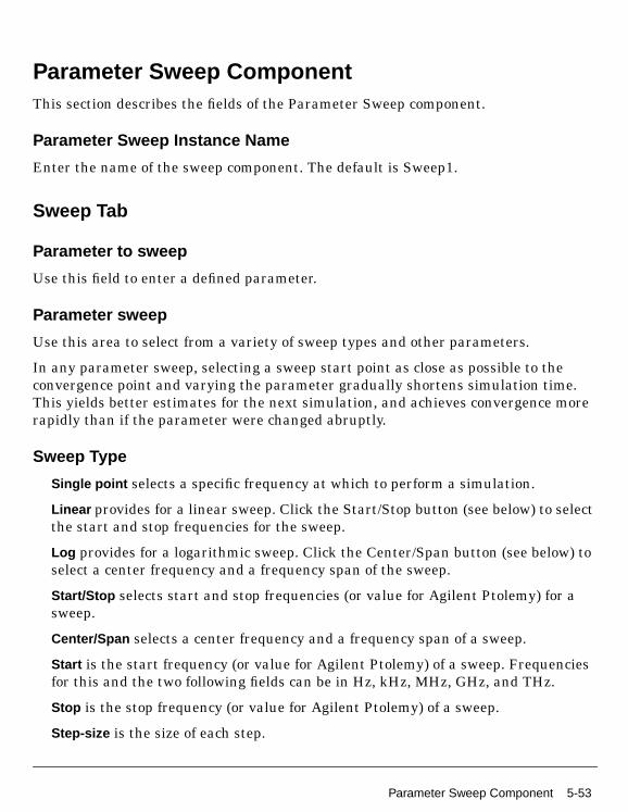
Parameter Sweep ComponentThis section describes the fields of the Parameter Sweep component.
Parameter Sweep Instance Name
Enter the name of the sweep component. The default is Sweep1.
Sweep Tab
Parameter to sweep
Use this field to enter a defined parameter.
Parameter sweep
Use this area to select from a variety of sweep types and other parameters.
In any parameter sweep, selecting a sweep start point as close as possible to theconvergence point and varying the parameter gradually shortens simulation time.This yields better estimates for the next simulation, and achieves convergence morerapidly than if the parameter were changed abruptly.
Sweep Type
Single point selects a specific frequency at which to perform a simulation.
Linear provides for a linear sweep. Click the Start/Stop button (see below) to selectthe start and stop frequencies for the sweep.
Log provides for a logarithmic sweep. Click the Center/Span button (see below) toselect a center frequency and a frequency span of the sweep.
Start/Stop selects start and stop frequencies (or value for Agilent Ptolemy) for asweep.
Center/Span selects a center frequency and a frequency span of a sweep.
Start is the start frequency (or value for Agilent Ptolemy) of a sweep. Frequenciesfor this and the two following fields can be in Hz, kHz, MHz, GHz, and THz.
Stop is the stop frequency (or value for Agilent Ptolemy) of a sweep.
Step-size is the size of each step.
Parameter Sweep Component 5-53

Simulation Control Items
Num. of pts. is the number of points over which the sweep is conducted.
A change to one of the above four fields causes the remaining fields to be calculatedautomatically.
Use sweep plan
To use a sweep plan (SweepPlan) that you have defined and named, select this optionand enter the name of the plan in the field.
Simulations Tab
Simulations to perform
Use this area to enter the name(s) of the simulation(s) you wish to perform (forexample, Simulation 1 = DC1, Simulation 2 = AC1, Simulation 3 = HB3). Simulationswill be performed in the sequence listed.
Display Tab
Lists and allows you to show or hide the parameters available with the selectedcomponent.
Set All shows all parameters.
Clear All hides all parameters.
Notes Some parameters must be displayed on the schematic to be edited.
To reduce screen clutter, keep visible only those parameters in which you areinterested. This also allows you to edit them directly on the schematic.
Whether a parameter is displayed or not does not affect its functionality. That isdetermined by settings elsewhere in the component.
5-54 Parameter Sweep Component

Budget LinearizationThis section includes information on the use of the BudLinearization component,which is available in the Harmonic Balance, LSSP, and XDB Simulation palettes, andmust be used in conjunction with those analyses.
Using the BudLinearization Component
To use the BudLinearization component, place the component in the schematic andedit it to reference the simulation component to be used, as well as the circuitcomponents that are to be linearized. If no component is specified, all the componentsin the top-level design are linearized one at a time.
The BudLinearization component first performs a regular harmonic balancesimulation, and then looks at the DC operating point for each nonlinear systemcomponent in turn, linearizing the response of that component while the responses ofthe remaining nonlinear system components remain nonlinear. If a systemcomponent is in a subcircuit, the entire subcircuit will be linearized.
The results of BudLinearization analysis are sorted in ascending order of the namesof the linearized components. LinearizedElementIndex, an integer independentvariable, is attached to the data as an additional sweep variable. The first pointcorresponds to the results of the regular harmonic balance simulation when none ofthe components is linearized. Another variable, LinearizedElement, that contains thenames of the linearized components is also generated.
Note The inclusion of the BudLinearization component in conjunction with aHarmonic Balance simulation causes N+1 harmonic balance simulations to be run,where N is the number of nonlinear components to be linearized. Consequently, sucha simulation will take N+1 times as long.
Budget Linearization 5-55

Simulation Control Items
Noise ComponentFollowing are details on the tabs and data fields for the NoiseCon component, whichis available from the Simulation - HB library.
NoiseCon Freq Tab
The frequency at which noise should be computed is specified on the Freq tab. If aphase noise simulation is to be performed, as specified on the PhaseNoise tab, theinterpretation of these noise frequencies is different. Instead of computing noisedirectly at these frequencies, they are interpreted as offset frequencies from a largesignal carrier which is specified on the PhaseNoise tab.
Noise frequency
Use this area to select the frequency(s) at which nonlinear noise is computed.
Sweep Type
Refer to “Sweep” on page 5-2
NoiseCon Nodes Tab
The nodes at which noise voltages and branches through which noise currents are tobe calculated are specified on this tab. Unlike the main harmonic balance simulation,noise is only computed at those nodes that the user specifies, not at all named nodes.If only the single sideband noise figure is to be computed, then no information needbe entered here.
Nodes for Calculation of Noise Parameters
Use this area to select nodes at which you want linear noise data to be reported.Noise voltages and currents are reported in rms units.
Note The fewer the number of nodes requested, the quicker the simulation and theless memory required.
Pos Node selects the named node(s) for the simulator to consider.
5-56 Noise Component

Neg Node allows differential noise measurements to be set up. This dialog allows theuser to specify a differential noise measurement between two nodes. Unlike aharmonic balance simulation, the noise voltage between two nodes cannot becomputed by first computing the noise voltage separately at each node andsubtracting the results, due to possible correlation between the noise at each node.Using a differential noise measurement here the correlation effects will beconsidered. To request a differential noise measurement, enter the first node as PosNode and the second node as Neg Node . The result in the dataset will have a name ofthe form HB1.NC1.posnode_minus_negnode . If a differential noise measurement is notrequired, leave the Neg Node field blank. Differential measurements are supportedonly for node voltages, not branch currents.
Select holds the names of the nodes the simulator will consider.
Add adds a named node.
Cut deletes a named node.
Paste takes a named node that has been cut and places it in a different order in theSelect window.
Include port noise causes port noise to be included in noise currents and voltages.Ports must be placed and defined. If Include port noise is selected, the thermal noisegenerated by the source resistance in frequency domain power sources and Termelements are included in the simulation results for noise voltages and currents. Thisdoes not affect the computation of noise figure.
NoiseCon Misc Tab
Input frequency
Because the simulator uses a single-sideband definition of noise figure, the correctinput sideband frequency must be specified here. This parameter identifies whichinput frequency will mix to the noise frequency of interest.
In the case of mixers, Input frequency is typically determined by an equation thatinvolves the local oscillator (LO) frequency and the noise frequency. Either the sum ofor difference between these two values is used, depending on whether upconversionor downconversion is taking place.
The above parameters do not need to be specified if only the output noise voltage isdesired (that is, if no noise figure is computed).
Noise Component 5-57
Simulation Control Items
Noise input port is the number of the source port at which noise is injected. This iscommonly the RF port. Although any valid port number can be used, the input portnumber is frequently defined as Num=1. If noise figure is not required, this fieldshould be blank.
Noise output port is the number of the Term component at which noise is retrieved.This is commonly the IF port. Although any valid port number can be used, the inputport number is frequently defined as Num=2. If noise figure is not required, this fieldshould be blank.
Noise contributors
Use this area to sort contributions to noise, as well as a threshold below which noisewill not be reported.
Mode provides the following options:
Off causes no individual noise contributors (nodes) to be selected. The result issimply a value for total noise at the node.
Sort by value sorts individual noise contributors, from largest to smallest, thatexceed a user-defined threshold (see below). The subcomponents of the nonlineardevices that generate noise (such as Rb, Rc, Re, Ib, and Ic in a BJT) are listedseparately, as well as the total noise from the device.
Sort by name causes individual noise contributors to be identified and sorts themalphabetically. The subcomponents of the nonlinear devices that generate noise(such as Rb, Rc, Re, Ib, and Ic in a BJT) are listed separately, as well as the totalnoise from the device
Sort by value with no device details sorts individual noise contributors, from largestto smallest, that exceed a user-defined threshold (see below). Unlike Sort by value,only the total noise from nonlinear devices is listed without any subcomponentdetails.
Sort by name with no device details causes individual noise contributors to beidentified and sorts them alphabetically. Unlike Sort by name, only the total noisefrom nonlinear devices is listed without subcomponent details.
Dynamic range to display is a threshold below the total noise, in dB, that determineswhat noise contributors are reported. All noise contributors less than this thresholdwill be reported. For example, assuming that the total noise voltage is 10 nV, asetting of 40 dB (a good typical value) ensures that all noise contributors up to 40 dB
5-58 Noise Component

below 10 nV (that is, above 0.1 nV) are reported. The default of 0 dB causes all noisecontributors to be reported. Accept the default if Sort by name is selected.
Calculate noisy two-port parameters causes an S-parameter simulation to beperformed. Ports must be placed and defined. The Noise input port parameter shouldbe set equal to the port number specified by the Num parameter on the input source,and the Noise output parameter to the number of the output Term (termination)component to Num=2. The following two-port parameters (dataset variables) arethen returned and can be plotted:
NFmin is the minimum noise figure of a two-port circuit. It is equal to the noisefigure when the optimum source admittance is connected to the circuit. (Its defaultunit is dB).
Sopt is the optimum source match for a two-port circuit. It is the reflectioncoefficient (looking into the source) that gives the minimum noise figure.
Rn is the effective noise resistance in ohms (unnormalized) of a two-port circuit.Effective noise resistance can be used to plot noise-figure circles or relatedquantities. This parameter determines how rapidly the minimum noise figuredeteriorates when the source impedance is not at its optimum value.
Icor is the noise current correlation matrix, in units of Amperes squared. Itdescribes the short circuit noise currents squared at each port, and the correlationbetween noise currents at different ports.
These expressions for noise simulation can be manipulated in equations.
Bandwidth is the bandwidth for spectral noise simulation. 1 Hz is the recommendedbandwidth for measurements of spectral noise power.
NoiseCon PhaseNoise Tab
This dialog is used to specify that a phase noise simulation should be performedinstead of a standard noise simulation. The default is None (mixer) , a standard noisesimulation where noise voltages are computed at the requested nodes at the noisefrequency specified in the Freq tab. When a NoiseCon is used, phase noise can besimulated for any type of circuit, not just an oscillator. For example, this makes itpossible to simulate the added phase noise due to an amplifier. Phase noise can alsobe computed around any large signal carrier frequency, not just the fundamentalfrequency of an oscillator. This makes it possible to simulate the phase noise after anoscillator signal passes through a frequency multiplier or mixer.
Noise Component 5-59

Simulation Control Items
The type of noise simulation to be performed is specified by the Phase Noise Typeselection box. There are five possibilities:
1. None (mixer) . Noise voltages are computed at the nodes specified at thefrequencies specified on the Freq tab. Noise results in the dataset are of theform HB1.NC1.vout.noise . There is no concept of a carrier frequency.
2. Phase noise spectrum . Single sideband phase noise is computed at the nodesspecified, treating the frequency information on the Freq tab as an offsetfrequency from the large signal carrier. See below on how to specify the largesignal carrier frequency. Noise results in the dataset are of the formHB1.NC1.vout.pnmx (and HB1.NC1.vout.pnfm for an oscillator only).
3. Relative vnoise spectrum . Rather than compute the single sideband phase noise,the noise voltage is computed both at the carrier frequency minus the offsetfrequency and at the carrier frequency plus the offset frequency. The results arepresent as a relative noise spectrum around zero, with the results extendingfrom minus the largest offset frequency to plus the largest offset frequency.Noise results in the dataset are of the form HB1.NC1.vout.noise .
4. Absolute vnoise spectrum . This is similar to the Relative vnoise spectrum , exceptthe resulting spectrum is presented as an absolute spectrum around the largesignal carrier frequency, extending from the carrier frequency minus the largestoffset frequency to the carrier frequency plus the largest offset frequency. Noiseresults in the dataset are of the form HB1.NC1.vout.noise .
5. Integrated over bandwidth . In this type of simulation, the noise spectrum is firstcomputed as in the absolute spectrum. But rather than the reporting theresults as a frequency spectrum, the noise power is integrated over thespectrum and reported as a single noise voltage. The noise power is integratedusing the Bandwidth specified on the Misc tab, from the carrier frequency minushalf the bandwidth to the carrier frequency plus half the bandwidth. The pointsused in the integration are controlled by the offset frequencies set up in the Freqtab. The largest offset frequency should be at least half of the noise bandwidthto avoid extrapolation of the results during integration. Noise results in thedataset are of the form HB1.NC1.vout.noise .
Specify phase noise carrier
The frequency of the large signal carrier used in all but the normal noise simulationare specified at the bottom of this tab. Any large signal carrier from the harmonicbalance simulation may serve as the carrier frequency for phase noise simulation.There are two ways to specify the carrier frequency:
5-60 Noise Component

• The frequency value may be specified directly by selecting the Frequency buttonand entering the frequency in the box below it. Either a number or a variablename may be entered. Since the frequency may not be precisely known in anoscillator, the simulator searches for the frequency closest to the user specifiedfrequency. If the difference between the user specified frequency and the actuallarge signal frequency exceeds 10%, a warning message will be issued. A carrierfrequency of zero cannot be entered directly as zero due to a limitation in thesimulator; enter a small value such as 1 Hz instead.
• The other method for specifying the carrier frequency is to enter it using theCarrier mixing indices . For example, the lower sideband mixing term in a mixerwould be entered as 1 and -1. The indices are listed in sequential order bycarrier.
NoiseCon Display Tab
Refer to “Display” on page 5-7.
Use user-specified initial conditions instructs the simulator to use user-specified initialconditions to compute the initial charges and fluxes in the circuit. The simulator willskip time=0 dc analysis.
When this option is enabled, the simulator uses the currents specified in the InitCondfield of the inductors and the branch voltages specified in the InitCond field of thecapacitors, as well as the node voltages specified in both the Simulation-TransientInitCond and Simulation-Transient InitCondByName components to compute theinitial charges and fluxes in the circuit. The voltage given in the capacitor's InitCondfield will take precedence over the voltage given in the Simulation-TransientInitCond and Simulation-Transient InitCondByName components if there is aconflict.
When the option is disabled and the Simulation-Transient InitCond and/orSimulation-Transient InitCondByName components are placed on the schematic, thesimulator will start the transient analysis with a DC analysis at time=0 and try toforce those node voltages identified in the Simulation-Transient InitCond and/orSimulation-Transient InitCondByName components to be close to the voltagesspecified. The values, if any, given in the InitCond field of the capacitors andinductors, however, will not be used.
Noise Component 5-61

Simulation Control Items
Setting Initial Conditions with InitCond Components
There are two elements for setting initial conditions in a transient simulationInitCond and InitCondbyName. InitCond and InitCondByName are used to providean initial DC value for transient analysis only. These elements attach the specifiedvoltage source with a series resistor to the specified node(s) to force a value. The DCsolution for the entire circuit is then calculated. This DC solution is then used as thestarting state for the transient analysis.
5-62 Noise Component

Node Set and Node Set by NameThe following sections provide details on the component NodeSet andNodeSetByName, which appear in all simulator component libraries.
Using Node Sets to Facilitate a Simulation
By placing a NodeSet or NodeSetByName component at strategic places in a circuit,you can instruct the DC simulator to begin its analysis at a given “best-guess”voltage. It is also possible to enter values for connection resistance.
Node sets can be used in any analysis, but are especially useful for:
• Circuits that are bistable, such as flip-flops or ring oscillators, to force it to aknown high or low state rather than letting the DC solver find the metastablestate halfway between high and low.
• Circuits that are isolated from DC by blocking capacitors.
NodeSet and NodeSetByName work in a two stage process. In the first stage, theseelements attach the specified voltage source with a series resistor to the specifiednode(s) to force a value. A DC solution for the entire circuit is then calculated. In thesecond stage, the forcing source and resistor are removed and the DC solution isrefined, using the previous DC solution as an initial guess.
If you choose to use a NodeSetByName component, you can specify a name tofacilitate the retrieval of voltage data in the dataset.
Descriptions of the two components follow.
NodeSet
Instance Name Displays and edits the name of the component.
Select Parameter Selects a voltage or resistance for editing. V (volts) is an estimatedinitial node voltage. R is connection resistance.
Add adds a voltage or resistance to the Select Parameter field.
Cut deletes a voltage or resistance from the Select Parameter field.
Paste copies a voltage or resistance that has been cut and places it in the SelectParameter field.
Node Set and Node Set by Name 5-63

Simulation Control Items
Optimization/Statistics Setup Opens a dialog box providing for the entry ofparameters related to optimization and statistics.
Display parameter on schematic Displays or hides a selected node on the schematic.
NodeSetByName
Instance Name Displays and edits the name of the component.
Select Parameter Selects a node name for editing. This name is associated with aninitial voltage V and a connection resistance R.
Add adds a node name from the Edit Node Name field to the Select Parameterfield.
Cut deletes a node name from the Select Parameter field.
Paste copies a node name that has been cut and places it in the Select Parameterfield.
Edit Node Name Selects a node name for editing, or for adding to the SelectParameter field.
More brings up a dialog box listing available node names. When the dialog boxappears, select a node name in the top field to appear in the Select a node namefield at the bottom. Edit the name, then click OK.
Voltage The initial voltage guess associated with the node name. Use this field toedit the voltage.
Resistance The connection resistance associated with the node name. Use this fieldto edit the resistance.
Display parameter on schematic Displays or hides a selected node name on theschematic.
5-64 Node Set and Node Set by Name

Instrument Control ItemsThis section describes the parameters for the instrument control items available inthe Simulation - Instruments component library. These items are used in several ofthe simulation templates, which are accessed from the Schematic window byselecting Insert > Template.
Instrument Control Items 5-65
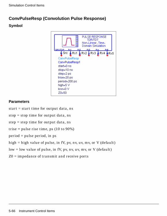
Simulation Control Items
ConvPulseResp (Convolution Pulse Response)
Symbol
Parameters
start = start time for output data, ns
stop = stop time for output data, ns
step = step time for output data, ns
trise = pulse rise time, ps (10 to 90%)
period = pulse period, in ps
high = high value of pulse, in fV, pv, nv, uv, mv, or V (default)
low = low value of pulse, in fV, pv, nv, uv, mv, or V (default)
Z0 = impedance of transmit and receive ports
5-66 Instrument Control Items

Notes
1. A template using this item can be accessed by selecting Insert > Template >ConvPulseRespT from the Schematic window.
2. ConvPulseResp emulates an instrument for measuring the reflection andtransmission of a network. The test signal is a pulse waveform, whosecharacteristics you specify. There is one source port, and five receive ports. Thesource port is also used to measure the reflected signal. The simulation iscarried out in the time domain, and if distributed elements are present in thenetwork being simulated, the convolution simulator will be used. The example,RF_Board/TDRcrosstalk_prj shows this component applied.
3. This is a simulation component. No other simulation or control components areneeded.
Instrument Control Items 5-67
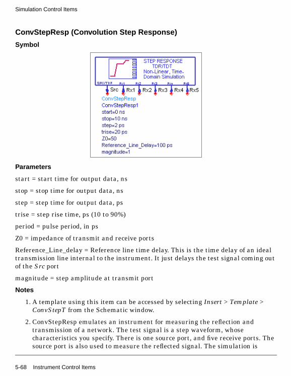
Simulation Control Items
ConvStepResp (Convolution Step Response)
Symbol
Parameters
start = start time for output data, ns
stop = stop time for output data, ns
step = step time for output data, ps
trise = step rise time, ps (10 to 90%)
period = pulse period, in ps
Z0 = impedance of transmit and receive ports
Reference_Line_delay = Reference line time delay. This is the time delay of an idealtransmission line internal to the instrument. It just delays the test signal coming outof the Src port
magnitude = step amplitude at transmit port
Notes
1. A template using this item can be accessed by selecting Insert > Template >ConvStepT from the Schematic window.
2. ConvStepResp emulates an instrument for measuring the reflection andtransmission of a network. The test signal is a step waveform, whosecharacteristics you specify. There is one source port, and five receive ports. Thesource port is also used to measure the reflected signal. The simulation is
5-68 Instrument Control Items

carried out in the time domain, and if distributed elements are present in thenetwork being simulated, the convolution simulator will be used. The example,RF_Board/TDRcrosstalk_prj shows this component applied.
3. This is a simulation component. No other simulation or control components areneeded.
Instrument Control Items 5-69

Simulation Control Items
DC_BJT (Curve Tracer for BJT
Symbol
Parameters
IBB_start = initial base current, in uA
IBB_stop = last base current, in uA
IBB_points = number of base current values
VCE_start = initial collector emitter voltage
VCE_stop = last collector emitter voltage
VCE_points = number of collector-emitter values
Notes
1. A template using this item can be accessed by selecting Insert > Template >DC_BJT_T from the Schematic window.
2. DC_BJT is a DC curve-tracer with a swept voltage source for the collector biasand a swept current source for the base bias.
3. This is a simulation component. No other simulation or control components areneeded.
5-70 Instrument Control Items

DC_FET (Curve Tracer for FET)
Symbol
Parameters
VGS_start = initial gate voltage
VGS_stop = last gate voltage
VGS_points = number of gate current values
VDS_start = initial drain-source voltage
VDS_stop = last drain-source voltage
VDS_points = number of drain-source values
Notes
1. A template using this item can be accessed by selecting Insert > Template >DC_FET_T from the Schematic window.
2. DC_FET is a DC curve-tracer with two swept voltage sources, one for the gatebias and the other for the drain bias.
3. This is a simulation component. No other simulation or control components areneeded.
Instrument Control Items 5-71

Simulation Control Items
LinearPulseResp (Pulse Response from Frequency Response)
Symbol
Parameters
start = start time for output data, ns
stop = stop time for output data, ns
step = step time for output data, ns
trise = pulse rise time, ps (10 to 90%)
period = pulse period, in ps
high = high value of pulse, in fV, pv, nv, uv, mv, or V (default)
low = low value of pulse, in fV, pv, nv, uv, mv, or V (default)
Z0 = impedance of transmit and receive ports
Notes
1. A template using this item can be accessed by selecting Insert > Template >LinearPulseRespT from the Schematic window.
2. LinearPulseResp emulates an instrument for measuring the reflection andtransmission of a network. The test signal is a pulse waveform, whosecharacteristics you specify. There is one source port, and five receive ports. Thesource port is also used to measure the reflected signal. The simulation iscarried out in the frequency domain, and the frequency-domain data is
5-72 Instrument Control Items

post-processed via the ts() function to get time-domain responses. If anynonlinear elements are included in the network being simulated, they will bemodeled as linear elements, linearized around their bias points. The example,RF_Board/TDRcrosstalk_prj shows this component applied.
3. This is a simulation component. No other simulation or control components areneeded.
Instrument Control Items 5-73

Simulation Control Items
LinearStepResp (Linear Response from Frequency Response)
Symbol
Parameters
start = start time for output data, ns
stop = stop time for output data, ns
step = step time, ps
trise = step rise time, ps (10 to 90%)
Z0 = impedance of transmit and receive ports
Reference_Line_delay = Reference line time delay
magnitude = step amplitude at transmit port
Notes
1. A template using this item can be accessed by selecting Insert > Template >LinearStepRespT from the Schematic window.
2. LinearStepResp emulates an instrument for measuring the reflection andtransmission of a network. The test signal is a step waveform, whosecharacteristics you specify. There is one source port, and five receive ports. Thesource port is also used to measure the reflected signal. The simulation iscarried out in the frequency domain, and the frequency-domain data ispost-processed via the ts() function to get time-domain responses. If anynonlinear elements are included in the network being simulated, they will be
5-74 Instrument Control Items

modeled as linear elements, linearized around their bias points. The example,RF_Board/TDRcrosstalk_prj shows this component applied.
3. This is a simulation component. No other simulation or control components areneeded.
Instrument Control Items 5-75
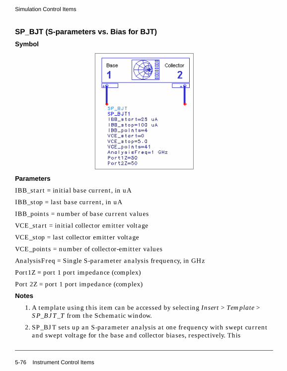
Simulation Control Items
SP_BJT (S-parameters vs. Bias for BJT)
Symbol
Parameters
IBB_start = initial base current, in uA
IBB_stop = last base current, in uA
IBB_points = number of base current values
VCE_start = initial collector emitter voltage
VCE_stop = last collector emitter voltage
VCE_points = number of collector-emitter values
AnalysisFreq = Single S-parameter analysis frequency, in GHz
Port1Z = port 1 port impedance (complex)
Port 2Z = port 1 port impedance (complex)
Notes
1. A template using this item can be accessed by selecting Insert > Template >SP_BJT_T from the Schematic window.
2. SP_BJT sets up an S-parameter analysis at one frequency with swept currentand swept voltage for the base and collector biases, respectively. This
5-76 Instrument Control Items

component helps select an operating point for desired gain. Connect it to abipolar junction transistor, as indicated in the schematic symbol.
3. This is a simulation component. No other simulation or control components areneeded.
Instrument Control Items 5-77

Simulation Control Items
SP_Diff (Differential-Mode S-Parameters)
Symbol
Parameters
Start = start frequency in Hz, KHz, GHz, or MHz (default)
Start = stop frequency in Hz, KHz, GHz, or MHz (default)
NumPoints = number of points in a linear sweep
Z1 = port 1 port impedance (complex)
Z2 = port2 port impedance (complex)
Notes
1. A template using this item can be accessed by selecting Insert > Template >SP_DiffT from the Schematic window.
2. SP_Diff sets up a swept-frequency S-parameter analysis. Ports 1 and 2 of theNetwork Analyzer are ungrounded, so the S-parameters of differentialnetworks can be simulated without using baluns.
3. This is a simulation component. No other simulation or control components areneeded.
5-78 Instrument Control Items
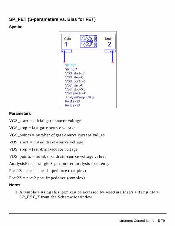
SP_FET (S-parameters vs. Bias for FET)
Symbol
Parameters
VGS_start = initial gate-source voltage
VGS_stop = last gate-source voltage
VGS_points = number of gate-source current values
VDS_start = initial drain-source voltage
VDS_stop = last drain-source voltage
VDS_points = number of drain-source voltage values
AnalysisFreq = single S-parameter analysis frequency
Port1Z = port 1 port impedance (complex)
Port2Z = port2 port impedance (complex)
Notes
1. A template using this item can be accessed by selecting Insert > Template >SP_FET_T from the Schematic window.
Instrument Control Items 5-79

Simulation Control Items
2. SP_FET sets up an S-parameter analysis at one frequency with two sweptvoltage, one each for the for the gate and drain bias. This component helpsselect an operating point for desired gain. Connect it to a field effect transistor,as indicated in the schematic symbol.
3. This is a simulation component. No other simulation or control components areneeded.
5-80 Instrument Control Items
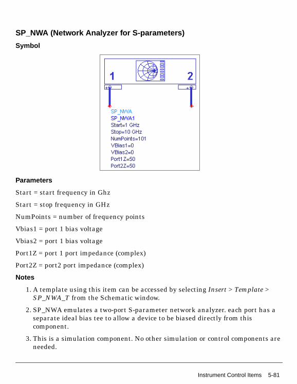
SP_NWA (Network Analyzer for S-parameters)
Symbol
Parameters
Start = start frequency in Ghz
Start = stop frequency in GHz
NumPoints = number of frequency points
Vbias1 = port 1 bias voltage
Vbias2 = port 1 bias voltage
Port1Z = port 1 port impedance (complex)
Port2Z = port2 port impedance (complex)
Notes
1. A template using this item can be accessed by selecting Insert > Template >SP_NWA_T from the Schematic window.
2. SP_NWA emulates a two-port S-parameter network analyzer. each port has aseparate ideal bias tee to allow a device to be biased directly from thiscomponent.
3. This is a simulation component. No other simulation or control components areneeded.
Instrument Control Items 5-81
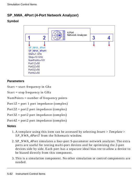
Simulation Control Items
SP_NWA_4Port (4-Port Network Analyzer)
Symbol
Parameters
Start = start frequency in Ghz
Start = stop frequency in GHz
NumPoints = number of frequency points
Port1Z = port 1 port impedance (complex)
Port2Z = port2 port impedance (complex)
Port3Z = port2 port impedance (complex)
Port4Z = port2 port impedance (complex)
Notes
1. A template using this item can be accessed by selecting Insert > Template >SP_NWA_4PortT from the Schematic window.
2. SP_NWA_4Port simulates a four-port S-parameter network analyzer. The extraports are useful for testing multi-port devices and for optimizing the 2-portdevices side by side. Each port has a separate ideal bias tee to allow a device tobe biased directly from this component.
3. This is a simulation component. No other simulation or control components areneeded.
5-82 Instrument Control Items

SP_NWA_4PortBias (4-Port Network Analyzer with Bias Sources)
Symbol
Parameters
Start = start frequency in GHz
Start = stop frequency in GHz
NumPoints = number of frequency points
V_DC1 = port 1 bias voltage
V_DC2 = port 2 bias voltage
V_DC3 = port 3 bias voltage
V_DC4 = port 4 bias voltage
Port1Z = port 1 port impedance (complex)
Port2Z = port2 port impedance (complex)
Port3Z = port2 port impedance (complex)
Port4Z = port2 port impedance (complex)
Instrument Control Items 5-83
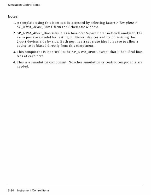
Simulation Control Items
Notes
1. A template using this item can be accessed by selecting Insert > Template >SP_NWA_4Port_BiasT from the Schematic window.
2. SP_NWA_4Port_Bias simulates a four-port S-parameter network analyzer. Theextra ports are useful for testing multi-port devices and for optimizing the2-port devices side by side. Each port has a separate ideal bias tee to allow adevice to be biased directly from this component.
3. This component is identical to the SP_NWA_4Port, except that it has ideal biastees at each port.
4. This is a simulation component. No other simulation or control components areneeded.
5-84 Instrument Control Items

SP_NWA_4PortBiasLog (4-Port Network Analyzer with Bias, Log Sweep)
Symbol
Parameters
Start = start frequency in GHz
Start = stop frequency in GHz
PointsperDec = number of frequency points per decade
V_DC1 = port 1 bias voltage
V_DC2 = port 2 bias voltage
V_DC3 = port 3 bias voltage
V_DC4 = port 4 bias voltage
Port1Z = port 1 port impedance (complex)
Port2Z = port2 port impedance (complex)
Port3Z = port2 port impedance (complex)
Port4Z = port2 port impedance (complex)
Instrument Control Items 5-85
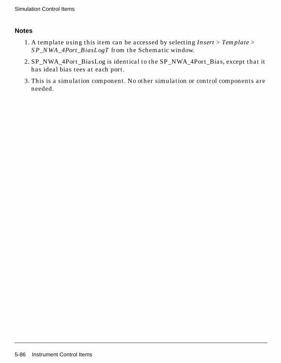
Simulation Control Items
Notes
1. A template using this item can be accessed by selecting Insert > Template >SP_NWA_4Port_BiasLogT from the Schematic window.
2. SP_NWA_4Port_BiasLog is identical to the SP_NWA_4Port_Bias, except that ithas ideal bias tees at each port.
3. This is a simulation component. No other simulation or control components areneeded.
5-86 Instrument Control Items

SP_NWA_4PortLog (4-Port Network Analyzer, Log Sweep)
Symbol
Parameters
Start = start frequency in kHz
Start = stop frequency in GHz
PointsPerDec = frequency points per decade
Port1Z = port 1 port impedance (complex)
Port2Z = port2 port impedance (complex)
Port3Z = port2 port impedance (complex)
Port4Z = port2 port impedance (complex)
Notes
1. A template using this item can be accessed by selecting Insert > Template >SP_NWA_4PortLogT from the Schematic window.
2. SP_NWA_4Port_Log is identical to SP_NWA_4Port, except the frequency isswept logarithmically. It simulates a four-port S-parameter network analyzer.The extra ports are useful for testing multi-port devices and for optimizing the2-port devices side by side. Each port has a separate ideal bias tee to allow adevice to be biased directly from this component.
Instrument Control Items 5-87

Simulation Control Items
3. This is a simulation component. No other simulation or control components areneeded.
5-88 Instrument Control Items
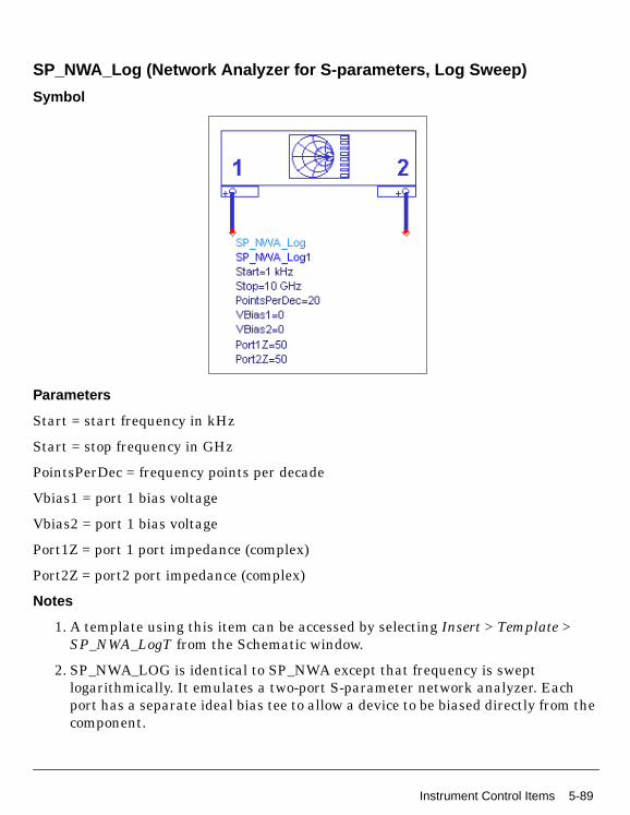
SP_NWA_Log (Network Analyzer for S-parameters, Log Sweep)
Symbol
Parameters
Start = start frequency in kHz
Start = stop frequency in GHz
PointsPerDec = frequency points per decade
Vbias1 = port 1 bias voltage
Vbias2 = port 1 bias voltage
Port1Z = port 1 port impedance (complex)
Port2Z = port2 port impedance (complex)
Notes
1. A template using this item can be accessed by selecting Insert > Template >SP_NWA_LogT from the Schematic window.
2. SP_NWA_LOG is identical to SP_NWA except that frequency is sweptlogarithmically. It emulates a two-port S-parameter network analyzer. Eachport has a separate ideal bias tee to allow a device to be biased directly from thecomponent.
Instrument Control Items 5-89

Simulation Control Items
3. This is a simulation component. No other simulation or control components areneeded.
5-90 Instrument Control Items

Chapter 6: Linear Data File Components
6-1

Linear Data File Components
Deembed1 (1-Port De-Embed Data File)
Symbol
Parameters
File = name of .s1p file containing 1-port S-, Y-, or Z-parameters for this component.The file extension and directory path are optional. Default extension is .s1p and thedefault directory is <prj>/data where <prj> is your current project directory.
Type = file type: Touchstone, Dataset, CITIfile
InterpMode = interpolation mode: Linear, Cubic Spline, Cubic, Value Lookup
InterpDom = interpolation domain: Data Based, Rectangular, Polar, DB
Temp = physical temperature, in °C
Range of Usage
Within the frequency range of the S-, Y-, or Z-parameter file
Notes/Equations/References
1. For details on data file format, refer to the Circuit Simulation manual.
2. One of the Deembed1 data file applications is to negate the 1-port subcircuit byusing this data file.
3. InterpDom defines the domains in that the two parts of a complex dependentvariable are interpolated:
Rectangular: transform to (real, imag) before interpolation
Polar: transfer to (mag, angle) before interpolation.
DB: transfer to (dB, angle) before interpolation
Data Based: (Series IV compatibility) uses Polar for S-parameters, Rectangularfor Y- and Z-parameters
4. If the S-parameters belong to a passive DUT, Temp is used to compute noiseperformance. If the S-parameters belong to an active DUT, Temp is ignored andthe component is assumed to be noiseless.
6-2 Deembed1 (1-Port De-Embed Data File)

5. For time-domain analysis, the impulse response used for transient will benoncausal. This model should not be used for transient or circuit envelopeanalysis.
6. This component has no default artwork associated with it.
Deembed1 (1-Port De-Embed Data File) 6-3

Linear Data File Components
Deembed2 (2-Port De-Embed File)
Symbol
Parameters
File = name of .s2p file containing 2-port S-, Y-, or Z-parameters for this component.The file extension and directory path are optional. Default extension is .s2p and thedefault directory is <prj>/data where <prj> is your current project directory.
Type = file type: Touchstone, Dataset, CITIfile
InterpMode = interpolation mode: Linear, Cubic Spline, Cubic, Value Lookup
InterpDom = interpolation domain: Data Based, Rectangular, Polar, DB
Temp = physical temperature, in °C
Range of Usage
Within the frequency range of the S-, G-, H-, Y-, or Z-parameter file
Notes/Equations/References
1. For details on data file format, refer to the Circuit Simulation manual.
2. One of the Deembed2 data file applications is to negate the 2-port subcircuit byusing this data file.
3. The 2-port S-parameters are assumed to be measured with pin 1 as the input,pin 2 as the output, and pin 3 as the common terminal.
4. InterpDom defines the domains in that the two parts of a complex dependentvariable are interpolated:
Rectangular: transform to (real, imag) before interpolation
Polar: transfer to (mag, angle) before interpolation.
DB: transfer to (dB, angle) before interpolation
Data Based: (Series IV compatibility) uses Polar for S-parameters, Rectangularfor Y- and Z-parameters
6-4 Deembed2 (2-Port De-Embed File)

5. If the file contains noise parameters, the noise performance of this component iscalculated using the noise parameters and Temp is ignored. If the noiseparameters are not specified and the S-parameters belong to a passivecomponent, noise performance is calculated based on S-parameters and Temp.If noise parameters are not specified and the S-parameters belong to an activecomponent, Temp is ignored and the component is assumed to be noiseless.
6. For time-domain analysis, the impulse response used for transient will benoncausal. This model should not be used for transient or circuit envelopeanalysis.
7. This component has no default artwork associated with it.
Deembed2 (2-Port De-Embed File) 6-5
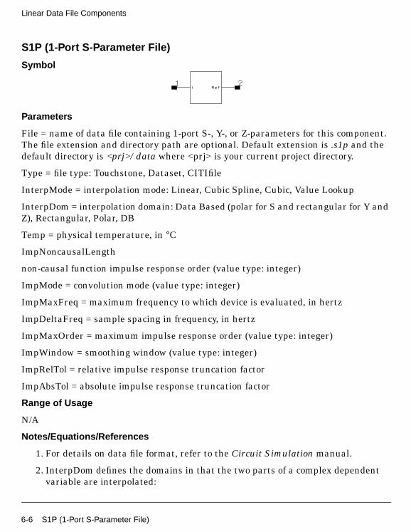
Linear Data File Components
S1P (1-Port S-Parameter File)
Symbol
Parameters
File = name of data file containing 1-port S-, Y-, or Z-parameters for this component.The file extension and directory path are optional. Default extension is .s1p and thedefault directory is <prj>/data where <prj> is your current project directory.
Type = file type: Touchstone, Dataset, CITIfile
InterpMode = interpolation mode: Linear, Cubic Spline, Cubic, Value Lookup
InterpDom = interpolation domain: Data Based (polar for S and rectangular for Y andZ), Rectangular, Polar, DB
Temp = physical temperature, in °C
ImpNoncausalLength
non-causal function impulse response order (value type: integer)
ImpMode = convolution mode (value type: integer)
ImpMaxFreq = maximum frequency to which device is evaluated, in hertz
ImpDeltaFreq = sample spacing in frequency, in hertz
ImpMaxOrder = maximum impulse response order (value type: integer)
ImpWindow = smoothing window (value type: integer)
ImpRelTol = relative impulse response truncation factor
ImpAbsTol = absolute impulse response truncation factor
Range of Usage
N/A
Notes/Equations/References
1. For details on data file format, refer to the Circuit Simulation manual.
2. InterpDom defines the domains in that the two parts of a complex dependentvariable are interpolated:
6-6 S1P (1-Port S-Parameter File)

Rectangular: transform to (real, imag) before interpolation
Polar: transfer to (mag, angle) before interpolation.
DB: transfer to (dB, angle) before interpolation
Data Based: (Series IV compatibility) uses Polar for S-parameters, Rectangularfor Y- and Z-parameters
3. Regarding the use of the InterpMode parameter: Interpolation of S-, Y-, orZ-parameters, PortZ reference impedance (and noise parameters for S2P) vs.simulation variable freq can be linear, cubic spline, cubic, or lookup by actualfreq value. The two parts of each complex parameter (RI, MA, dBA) areinterpolated independently.
4. If the S-parameters belong to a passive DUT, Temp is used to compute noiseperformance. If the S-parameters belong to an active DUT, Temp is ignored andthe component is assumed to be noiseless.
5. Allowed values for ImpMode are 1 (Discrete) and 2 (PWL Continuous).
Allowed values for ImpWindow are 0 (Rectangle) and 1 (Hanning).
If these values are not specified, they default to the corresponding globalparameter values specified by the transient analysis controller item. Refer toChapter 33, Simulation - Transient for default values on these parameters anda more detailed description of their use.
6. For time-domain analysis, the frequency-domain S-parameters are used.
7. This component has no default artwork associated with it.
S1P (1-Port S-Parameter File) 6-7

Linear Data File Components
S2P (2-Port S-Parameter File)
Symbol
Parameters
File = name of data file containing 2-port S-, Y-, or Z-parameters for this component.The file extension and directory path are optional. Default extension is .s2p and thedefault directory is <prj>/data where <prj> is your current project directory.
Type = file type: Touchstone, Dataset, CITIfile
InterpMode = interpolation mode: Linear, Cubic Spline, Cubic, Value Lookup
InterpDom = interpolation domain: Data Based (polar for S and rectangular for Y andZ), Rectangular, Polar, DB
Temp = physical temperature, in °C
ImpNoncausalLength = non-causal function impulse response order (value type:integer)
ImpMode = convolution mode (value type: integer)
ImpMaxFreq = maximum frequency to which device is evaluated, in hertz
ImpDeltaFreq = sample spacing in frequency, in hertz
ImpMaxOrder = maximum impulse response order (value type: integer)
ImpWindow = smoothing window (value type: integer)
ImpRelTol = relative impulse response truncation factor
ImpAbsTol = absolute impulse response truncation factor
Range of Usage
N/A
Notes/Equations/References
1. For details on data file formats, refer to the Circuit Simulation manual.
6-8 S2P (2-Port S-Parameter File)

2. The 2-port S-parameters are assumed to be measured with pin 1 as the input,pin 2 as the output, and pin 3 as the common terminal.
3. InterpDom defines the domains in that the two parts of a complex dependentvariable are interpolated:
Rectangular: transform to (real, imag) before interpolation
Polar: transfer to (mag, angle) before interpolation.
DB: transfer to (dB, angle) before interpolation
Data Based: (Series IV compatibility) uses Polar for S-parameters, Rectangularfor Y- and Z-parameters
4. Regarding the use of the InterpMode parameter: Interpolation of S-, Y-, orZ-parameters, PortZ reference impedance (and noise parameters for S2P) vs.simulation variable freq can be linear, cubic spline, cubic, or lookup by actualfreq value. The two parts of each complex parameter (RI, MA, dBA) areinterpolated independently.
5. If the file contains noise parameters, the noise performance of this component iscalculated using the noise parameters and Temp is ignored. If the noiseparameters are not specified and the S-parameters belong to a passivecomponent, noise performance is calculated based on S-parameters and Temp.If noise parameters are not specified and the S-parameters belong to an activecomponent, Temp is ignored and the component is assumed to be noiseless.
6. Allowed values for ImpMode are 1 (Discrete) and 2 (PWL Continuous).
Allowed values for ImpWindow are 0 (Rectangle) and 1 (Hanning).
If these values are not specified, they default to the corresponding globalparameter values specified by the transient analysis controller item.
7. For time-domain analysis, the frequency-domain S-parameters are used.
8. This component has no default artwork associated with it.
S2P (2-Port S-Parameter File) 6-9
Linear Data File Components
S2P_Conn (2-Port S-Parameter File; connector artwork)
Symbol
Parameters
File = name of data file containing 2-port S-, Y-, or Z-parameters for this component.The file extension and directory path are optional. Default extension is .s2p and thedefault directory is <prj>/data where <prj> is your current project directory.
Type = file type: Touchstone, Dataset. CITIfile, Value
InterpMode = interpolation mode: Linear, Cubic Spline, Cubic, Value Lookup, CeilingValue Lookup, Floor Value Lookup, Value
InterpDom = interpolation domain: Data Based (polar for S and rectangular for Y andZ), Rectangular, Polar, DB
Temp = physical temperature, in °C
Side = top or bottom
Range of Usage
S-, G-, Y-, or Z-parameters
Notes/Equations/References
1. For details on data file formats, refer to the Circuit Simulation manual.
2. The 2-port S-parameters are assumed to be measured with pin 1 as the input,pin 2 as the output, and pin 3 as the common terminal.
3. InterpDom defines the domains in that the two parts of a complex dependentvariable are interpolated:
Rectangular: transform to (real, imag) before interpolation
Polar: transfer to (mag, angle) before interpolation.
DB: transfer to (dB, angle) before interpolation
Data Based: (Series IV compatibility) uses Polar for S-parameters, Rectangularfor Y- and Z-parameters
6-10 S2P_Conn (2-Port S-Parameter File; connector artwork)

4. Regarding the use of the InterpMode parameter: Interpolation of S-, Y-, orZ-parameters, PortZ reference impedance (and noise parameters for S2P) vs.simulation variable freq can be linear, cubic spline, cubic, or lookup by actualfreq value. The two parts of each complex parameter (RI, MA, dBA) areinterpolated independently.
5. If the file contains noise parameters, the noise performance of this component iscalculated using the noise parameters and Temp is ignored. If the noiseparameters are not specified and the S-parameters belong to a passivecomponent, noise performance is calculated based on S-parameters and Temp.If noise parameters are not specified and the S-parameters belong to an activecomponent, Temp is ignored and the component is assumed to be noiseless.
6. Allowed values for ImpMode are 1 (Discrete) and 2 (PWL Continuous).
Allowed values for ImpWindow are 0 (Rectangle) and 1 (Hanning).
If these values are not specified, they default to the corresponding globalparameter values specified by the transient analysis controller item.
7. For transient analysis, pins 1 and 2 are shorted together.
8. For convolution analysis, the frequency-domain S-parameters are used.
S2P_Conn (2-Port S-Parameter File; connector artwork) 6-11

Linear Data File Components
S2P_PAD3 (2-Port S-Parameter File; pad artwork)
Symbol
Parameters
File = name of data file containing 2-port S-, Y-, or Z-parameters for this component.The file extension and directory path are optional. Default extension is .s2p and thedefault directory is <prj>/data where <prj> is your current project directory.
Type = file type: Touchstone, Dataset, CITIfile, Value
InterpMode = interpolation mode: Linear, Cubic Spline, Cubic, Value Lookup, CeilingValue Lookup, Floor Value Lookup, Value
InterpDom = interpolation domain: Data Based (polar for S and rectangular for Y andZ), Rectangular, Polar, DB
Temp = physical temperature, in °C
W1 = (for Layout Option) width of line at pins 1 and 2, in length units
W2 = (for Layout Option) width of line at pin 3, in length units
S = (for Layout Option) spacing (length from pin1 to pin 2, in length units
L1 = (for Layout Option) length from pin 1 to pin 2, in length units
L2 = (for Layout Option) length between pin 3 to pins 1 and 2, in length units
Side = top, bottom
Range of Usage
S-, G-, H-, Y-, or Z-parameters
Notes/Equations/References
1. For details on data file formats, refer to the Circuit Simulation manual.
2. The 2-port S-parameters are assumed to be measured with pin 1 as the input,pin 2 as the output, and pin 3 as the common terminal.
3. InterpDom defines the domains in that the two parts of a complex dependentvariable are interpolated:
6-12 S2P_PAD3 (2-Port S-Parameter File; pad artwork)

Rectangular: transform to (real, imag) before interpolation
Polar: transfer to (mag, angle) before interpolation.
DB: transfer to (dB, angle) before interpolation
Data Based: (Series IV compatibility) uses Polar for S-parameters, Rectangularfor Y- and Z-parameters
4. Regarding the use of the InterpMode parameter: Interpolation of S-, Y-, orZ-parameters, PortZ reference impedance (and noise parameters for S2P) vs.simulation variable freq can be linear, cubic spline, cubic, or lookup by actualfreq value. The two parts of each complex parameter (RI, MA, dBA) areinterpolated independently.
5. If the file contains noise parameters, the noise performance of this component iscalculated using the noise parameters and Temp is ignored. If the noiseparameters are not specified and the S-parameters belong to a passivecomponent, noise performance is calculated based on S-parameters and Temp.If noise parameters are not specified and the S-parameters belong to an activecomponent, Temp is ignored and the component is assumed to be noiseless.
6. Allowed values for ImpMode are 1 (Discrete) and 2 (PWL Continuous).
Allowed values for ImpWindow are 0 (Rectangle) and 1 (Hanning).
If these values are not specified, they default to the corresponding globalparameter values specified by the transient analysis controller item. Refer toChapter 33, Simulation - Transient for default values on these parameters anda more detailed description of their use.
7. For transient analysis, pins 1 and 2 are shorted together.
8. For convolution analysis, the frequency-domain S-parameters are used.
S2P_PAD3 (2-Port S-Parameter File; pad artwork) 6-13

Linear Data File Components
S2PMDIF (Multi-Dimensional 2-Port S-parameter File)
Symbol
Parameters
File = name of MDIF file containing 2-port S-, G-, H-, Y-, or Z-parameters for thiscomponent, with optional noise parameters. The file extension and directory path areoptional. Default extension is .s2p and the default directory is <prj>/data where<prj> is your current project directory.
Type = file type: S2PMDIF, Touchstone, Dataset, CITIfile
InterpMode = interpolation mode: Linear, Cubic Spline, Cubic, Value Lookup
InterpDom = interpolation domain: Data Based (polar for S and rectangular for Y andZ), Rectangular, Polar, DB
Temp = physical temperature, in °C
ImpNoncausalLength = non-causal function impulse response order (value type:integer)
ImpMode = convolution mode (value type: integer)
ImpMaxFreq = maximum frequency to which device is evaluated, in hertz
ImpDeltaFreq = sample spacing in frequency, in hertz
ImpMaxOrder = maximum impulse response order (value type: integer)
ImpWindow = smoothing window (value type: integer)
ImpRelTol = relative impulse response truncation factor
ImpAbsTol = absolute impulse response truncation factor
Range of Usage
N/A
Notes/Equations/References
1. For details on data file format, refer to the Circuit Simulation manual.
6-14 S2PMDIF (Multi-Dimensional 2-Port S-parameter File)
2. InterpDom defines the domains in that the two parts of a complex dependentvariable are interpolated:
Rectangular: transform to (real, imag) before interpolation
Polar: transfer to (mag, angle) before interpolation.
DB: transfer to (dB, angle) before interpolation
Data Based: (Series IV compatibility) uses Polar for S-parameters, Rectangularfor Y- and Z-parameters
3. Regarding the use of the InterpMode parameter: Interpolation of S-, Y-, orZ-parameters, PortZ reference impedance (and noise parameters for S2P) vs.simulation variable freq can be linear, cubic spline, cubic, or lookup by actualfreq value. The two parts of each complex parameter (RI, MA, dBA) areinterpolated independently.
4. Noise parameters (optimum source reflection coefficient, minimum noise figurein dB and effective source resistance) can be present in the file. If the filecontains noise parameters, the noise performance of this component iscalculated using the noise parameters and Temp is ignored. If the noiseparameters are not specified and the S-parameters belong to a passivecomponent, noise performance is calculated based on S-parameters and Temp.If noise parameters are not specified and the S-parameters belong to an activecomponent, Temp is ignored and the component is assumed to be noiseless.
Allowed values for ImpMode are 1 (Discrete) and 2 (PWL Continuous). Allowedvalues for ImpWindow are 0 (Rectangle) and 1 (Hanning). If ImpMode, If thesevalues are not specified, they default to the corresponding global parametervalues specified by the transient analysis controller item. Refer to Chapter 33,Simulation - Transient for default values on these parameters and a moredetailed description of their use.
5. For time-domain analysis, the frequency-domain S-parameters are used.
6. Note that a string iVar parameter is searched in a case-preferential manner, i.e.,it is searched in a case-sensitive manner, failing that, it is searched again in acase-insensitive manner.
7. This component has no default artwork associated with it.
S2PMDIF (Multi-Dimensional 2-Port S-parameter File) 6-15
Linear Data File Components
S2P_Spac (2-Port S-Parameter File)
Symbol
Parameters
File = name of data file containing 2-port S-, Y-, or Z-parameters for this component.The file extension and directory path are optional. Default extension is .s2p and thedefault directory is <prj>/data where <prj> is your current project directory.
Type = file type: Touchstone, Dataset, CITIfile, Value
InterpMode = interpolation mode: Linear, Cubic Spline, Cubic, Value Lookup, CeilingValue Lookup, Floor Value Lookup, Value
InterpDom = interpolation domain: Data Based (polar for S and rectangular for Y andZ), Rectangular, Polar, DB
Temp = physical temperature, in °C
L = length (meter, mil, in, ft)
Side = top, bottom
Range of Usage
S-, G-, H-, Y-, or Z-parameters
Notes/Equations/References
1. For details on data file formats, refer to the Circuit Simulation manual.
2. The 2-port S-parameters are assumed to be measured with pin 1 as the input,pin 2 as the output, and pin 3 as the common terminal.
3. InterpDom defines the domains in that the two parts of a complex dependentvariable are interpolated:
Rectangular: transform to (real, imag) before interpolation
Polar: transfer to (mag, angle) before interpolation.
DB: transfer to (dB, angle) before interpolation
6-16 S2P_Spac (2-Port S-Parameter File)
Data Based: (Series IV compatibility) uses Polar for S-parameters, Rectangularfor Y- and Z-parameters
4. Regarding the use of the InterpMode parameter: Interpolation of S-, Y-, orZ-parameters, PortZ reference impedance (and noise parameters for S2P) vs.simulation variable freq can be linear, cubic spline, cubic, or lookup by actualfreq value. The two parts of each complex parameter (RI, MA, dBA) areinterpolated independently.
5. If the file contains noise parameters, the noise performance of this component iscalculated using the noise parameters and Temp is ignored. If the noiseparameters are not specified and the S-parameters belong to a passivecomponent, noise performance is calculated based on S-parameters and Temp.If noise parameters are not specified and the S-parameters belong to an activecomponent, Temp is ignored and the component is assumed to be noiseless.
6. Allowed values for ImpMode are 1 (Discrete) and 2 (PWL Continuous).
Allowed values for ImpWindow are 0 (Rectangle) and 1 (Hanning).
If these values are not specified, they default to the corresponding globalparameter values specified by the transient analysis controller item.
7. For time-domain analysis, the frequency-domain S-parameters are used.
8. This component has no default artwork associated with it.
9. For transient analysis, pins 1 and 2 are shorted together.
10. For convolution analysis, the frequency-domain S-parameters are used.
11. This component is represented as a connected gap in layout -- into which acustom artwork object can be inserted.
S2P_Spac (2-Port S-Parameter File) 6-17
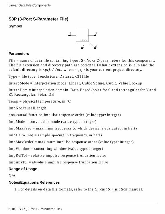
Linear Data File Components
S3P (3-Port S-Parameter File)
Symbol
Parameters
File = name of data file containing 3-port S-, Y-, or Z-parameters for this component.The file extension and directory path are optional. Default extension is .s3p and thedefault directory is <prj>/data where <prj> is your current project directory.
Type = file type: Touchstone, Dataset, CITIfile
InterpMode = interpolation mode: Linear, Cubic Spline, Cubic, Value Lookup
InterpDom = interpolation domain: Data Based (polar for S and rectangular for Y andZ), Rectangular, Polar, DB
Temp = physical temperature, in °C
ImpNoncausalLength
non-causal function impulse response order (value type: integer)
ImpMode = convolution mode (value type: integer)
ImpMaxFreq = maximum frequency to which device is evaluated, in hertz
ImpDeltaFreq = sample spacing in frequency, in hertz
ImpMaxOrder = maximum impulse response order (value type: integer)
ImpWindow = smoothing window (value type: integer)
ImpRelTol = relative impulse response truncation factor
ImpAbsTol = absolute impulse response truncation factor
Range of Usage
N/A
Notes/Equations/References
1. For details on data file formats, refer to the Circuit Simulation manual.
6-18 S3P (3-Port S-Parameter File)
2. InterpDom defines the domains in that the two parts of a complex dependentvariable are interpolated:
Rectangular: transform to (real, imag) before interpolation
Polar: transfer to (mag, angle) before interpolation.
DB: transfer to (dB, angle) before interpolation
Data Based: (Series IV compatibility) uses Polar for S-parameters, Rectangularfor Y- and Z-parameters
3. Regarding the use of the InterpMode parameter: Interpolation of S-, Y-, orZ-parameters, PortZ reference impedance (and noise parameters for S2P) vs.simulation variable freq can be linear, cubic spline, cubic, or lookup by actualfreq value. The two parts of each complex parameter (RI, MA, dBA) areinterpolated independently.
4. If the S-parameters belong to a passive DUT, Temp is used to compute the noiseperformance of the S3P component; if the S-parameters belong to an activeDUT, Temp is ignored and the component is assumed to be noiseless.
5. Allowed values for ImpMode are 1 (Discrete) and 2 (PWL Continuous).
Allowed values for ImpWindow are 0 (Rectangle) and 1 (Hanning).
If these values are not specified, they default to the corresponding globalparameter values specified by the transient analysis controller item. Refer toChapter 33, Simulation - Transient for default values on these parameters anda more detailed description of their use.
6. For time-domain analysis, the frequency-domain S-parameters are used.
7. This component has no default artwork associated with it.
S3P (3-Port S-Parameter File) 6-19

Linear Data File Components
S4P (4-Port S-Parameter File)
Symbol
Parameters
File = name of data file containing 4-port S-, Y-, or Z-parameters for this component.The file extension and directory path are optional. Default extension is .s4p and thedefault directory is <prj>/data where <prj> is your current project directory.
Type = file type: Touchstone, Dataset, CITIfile
InterpMode = interpolation mode: Linear, Cubic Spline, Cubic, Value Lookup
InterpDom = interpolation domain: Data Based (polar for S and rectangular for Y andZ), Rectangular, Polar, DB
Temp = physical temperature, in °C
ImpNoncausalLength = non-causal function impulse response order (value type:integer)
ImpMode = convolution mode (value type: integer)
ImpMaxFreq = maximum frequency to which device is evaluated, in hertz
ImpDeltaFreq = sample spacing in frequency, in hertz
ImpMaxOrder = maximum impulse response order (value type: integer)
ImpWindow = smoothing window (value type: integer)
ImpRelTol = relative impulse response truncation factor
ImpAbsTol = absolute impulse response truncation factor
Range of Usage
N/A
6-20 S4P (4-Port S-Parameter File)

Notes/Equations/References
1. For details on data file formats, refer to the Circuit Simulation manual.
2. InterpDom defines the domains in that the two parts of a complex dependentvariable are interpolated:
Rectangular: transform to (real, imag) before interpolation
Polar: transfer to (mag, angle) before interpolation.
DB: transfer to (dB, angle) before interpolation
Data Based: (Series IV compatibility) uses Polar for S-parameters, Rectangularfor Y- and Z-parameters
3. Regarding the use of the InterpMode parameter: Interpolation of S-, Y-, orZ-parameters, PortZ reference impedance (and noise parameters for S2P) vs.simulation variable freq can be linear, cubic spline, cubic, or lookup by actualfreq value. The two parts of each complex parameter (RI, MA, dBA) areinterpolated independently.
4. Allowed values for ImpMode are 1 (Discrete) and 2 (PWL Continuous).
Allowed values for ImpWindow are 0 (Rectangle) and 1 (Hanning).
If these values are not specified, they default to the corresponding globalparameter values specified by the transient analysis controller item. Refer toChapter 33, Simulation - Transient for default values on these parameters anda more detailed description of their use.
5. For time-domain analysis, the frequency-domain S-parameters are used.
6. This component has no default artwork associated with it.
S4P (4-Port S-Parameter File) 6-21

Linear Data File Components
S5P to S9P (5-Port to 9-Port S-Parameter File)
Symbol
Parameters
File = name of data file containing #-port S-, Y-, or Z-parameters for this component.The file extension and directory path are optional. Default extension is .s#p and thedefault directory is <prj>/data where <prj> is your current project directory.
Type = file type: Touchstone, Dataset, CITIfile
InterpMode = interpolation mode: Linear, Cubic Spline, Cubic, Value Lookup
InterpDom = interpolation domain: Data Based (polar for S and rectangular for Y andZ), Rectangular, Polar, DB
Temp = physical temperature, in °C
ImpNoncausalLength = non-causal function impulse response order (value type:integer)
ImpMode = convolution mode (value type: integer)
ImpMaxFreq = maximum frequency to which device is evaluated, in hertz
ImpDeltaFreq = sample spacing in frequency, in hertz
ImpMaxOrder = maximum impulse response order (value type: integer)
ImpWindow = smoothing window (value type: integer)
ImpRelTol = relative impulse response truncation factor
ImpAbsTol = absolute impulse response truncation factor
Range of Usage
N/A
6-22 S5P to S9P (5-Port to 9-Port S-Parameter File)
Notes/Equations/References
1. The number of terminals increases sequentially from 5 to 9, and is equal to thenumber of ports of the component.
2. For details on data file formats, refer to the Circuit Simulation manual.
3. If no extension is supplied with the file name, then a default value of “.s(#)p” isused, where (#) is the number of ports of the component.
4. InterpDom defines the domains in that the two parts of a complex dependentvariable are interpolated:
Rectangular: transform to (real, imag) before interpolation
Polar: transfer to (mag, angle) before interpolation.
DB: transfer to (dB, angle) before interpolation
Data Based: (Series IV compatibility) uses Polar for S-parameters, Rectangularfor Y- and Z-parameters
5. Regarding the use of the InterpMode parameter: Interpolation of S-, Y-, orZ-parameters, PortZ reference impedance (and noise parameters for S2P) vs.simulation variable freq can be linear, cubic spline, cubic, or lookup by actualfreq value. The two parts of each complex parameter (RI, MA, dBA) areinterpolated independently.
6. Allowed values for ImpMode are 1 (Discrete) and 2 (PWL Continuous).
Allowed values for ImpWindow are 0 (Rectangle) and 1 (Hanning).
If these values are not specified, they default to the corresponding globalparameter values specified by the transient analysis controller item. Refer toChapter 33, Simulation - Transient for default values on these parameters anda more detailed description of their use.
7. For time-domain analysis, the frequency-domain S-parameters are used.
8. This component has no default artwork associated with it.
6-23

Linear Data File Components
S10P to S20P (10-Port to 20-Port S-Parameter File)
Symbol
Parameters
File = name of data file containing #-port S-, Y-, or Z-parameters for this component.The file extension and directory path are optional. Default extension is .s#p and thedefault directory is <prj>/data where <prj> is your current project directory.
Type = file type: Touchstone, Dataset, CITIfile
InterpMode = interpolation mode: Linear, Cubic Spline, Cubic, Value Lookup
InterpDom = interpolation domain: Data Based (polar for S and rectangular for Y andZ), Rectangular, Polar, DB
Temp = physical temperature, in °C
ImpNoncausalLength = non-causal function impulse response order (value type:integer)
ImpMode = convolution mode (value type: integer)
ImpMaxFreq = maximum frequency to which device is evaluated, in hertz
ImpDeltaFreq = sample spacing in frequency, in hertz
ImpMaxOrder = maximum impulse response order (value type: integer)
ImpWindow = smoothing window (value type: integer)
ImpRelTol = relative impulse response truncation factor
ImpAbsTol = absolute impulse response truncation factor
6-24
Range of Usage
N/A
Notes/Equations/References
1. The items S11P through S99P cannot be selected from the component palette.They are accessed by typing the appropriate name (such as S12P or S98P) intothe right entry box (directly above the viewing area), pressing Enter, thenmoving the cursor to the viewing area to place the item.
2. The number of terminals increases sequentially from 10 to 20, and is equal tothe number of ports of the component.
3. For details on data file formats, refer to the Circuit Simulation manual.
4. If no extension is supplied with the File name, then a default value of “.s(#)p” isused, where (#) is the number of ports of the component.
5. InterpDom defines the domains in that the two parts of a complex dependentvariable are interpolated:
Rectangular: transform to (real, imag) before interpolation
Polar: transfer to (mag, angle) before interpolation.
DB: transfer to (dB, angle) before interpolation
Data Based: (Series IV compatibility) uses Polar for S-parameters, Rectangularfor Y- and Z-parameters
6. Regarding the use of the InterpMode parameter: Interpolation of S-, Y-, orZ-parameters, PortZ reference impedance (and noise parameters for S2P) vs.simulation variable freq can be linear, cubic spline, cubic, or lookup by actualfreq value. The two parts of each complex parameter (RI, MA, dBA) areinterpolated independently.
7. Allowed values for ImpMode are 1 (Discrete) and 2 (PWL Continuous).
Allowed values for ImpWindow are 0 (Rectangle) and 1 (Hanning).
If these values are not specified, they default to the corresponding globalparameter values specified by the transient analysis controller item. Refer toChapter 33, Simulation - Transient for default values on these parameters anda more detailed description of their use.
8. For time-domain analysis, the frequency-domain S-parameters are used.
6-25

Linear Data File Components
9. This component has no default artwork associated with it.
6-26
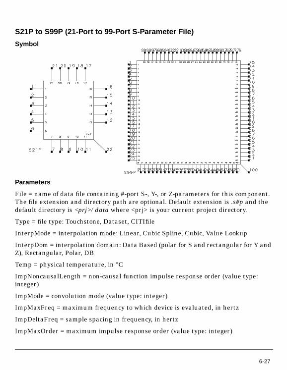
S21P to S99P (21-Port to 99-Port S-Parameter File)
Symbol
Parameters
File = name of data file containing #-port S-, Y-, or Z-parameters for this component.The file extension and directory path are optional. Default extension is .s#p and thedefault directory is <prj>/data where <prj> is your current project directory.
Type = file type: Touchstone, Dataset, CITIfile
InterpMode = interpolation mode: Linear, Cubic Spline, Cubic, Value Lookup
InterpDom = interpolation domain: Data Based (polar for S and rectangular for Y andZ), Rectangular, Polar, DB
Temp = physical temperature, in °C
ImpNoncausalLength = non-causal function impulse response order (value type:integer)
ImpMode = convolution mode (value type: integer)
ImpMaxFreq = maximum frequency to which device is evaluated, in hertz
ImpDeltaFreq = sample spacing in frequency, in hertz
ImpMaxOrder = maximum impulse response order (value type: integer)
6-27
Linear Data File Components
ImpWindow = smoothing window (value type: integer)
ImpRelTol = relative impulse response truncation factor
ImpAbsTol = absolute impulse response truncation factor
Range of Usage
N/A
Notes/Equations/References
1. The items S11P through S99P cannot be selected from the component palette.They are accessed by typing the appropriate name (such as S12P or S98P) intothe right entry box (directly above the viewing area), pressing Enter, thenmoving the cursor to the viewing area to place the item.
2. To support up to 99-port networks, the port number of a Port component can goup to 99.
3. The SMAT, YMAT, ZMAT, and NMAT measurements are allowed for up to99-port networks. However, single measurements such as SIJ, GD, and VSWRare only applicable for up to 20-port networks.
4. These components primarily support electromagnetic simulation results ofcircuits with a large number of ports, such as antenna feed networks.
5. InterpDom defines the domains in that the two parts of a complex dependentvariable are interpolated:
Rectangular: transform to (real, imag) before interpolation
Polar: transfer to (mag, angle) before interpolation.
DB: transfer to (dB, angle) before interpolation
Data Based: (Series IV compatibility) uses Polar for S-parameters, Rectangularfor Y- and Z-parameters
6. Regarding the use of the InterpMode parameter: Interpolation of S-, Y-, orZ-parameters, PortZ reference impedance (and noise parameters for S2P) vs.simulation variable freq can be linear, cubic spline, cubic, or lookup by actualfreq value. The two parts of each complex parameter (RI, MA, dBA) areinterpolated independently.
Allowed values for ImpMode are 1 (Discrete) and 2 (PWL Continuous).Allowed values for ImpWindow are 0 (Rectangle) and 1 (Hanning).If these values are not specified, they default to the corresponding global
6-28

parameter values specified by the transient analysis controller item. Refer toChapter 33, Simulation - Transient for default values on these parameters anda more detailed description of their use.
7. For time-domain analysis, the frequency-domain S-parameters are used.
8. This component has no default artwork associated with it.
6-29

Linear Data File Components
6-30

Chapter 7: Equation-Based LinearComponents
7-1

Equation-Based Linear Components
Chain (2-Port User-Defined Linear Chain)
Symbol
Parameters
A = reverse voltage gain (v1/v2 with i2=0)
B = reverse transresistance, in ohms (v1/i2 with v2=0)
C = reverse transconductance, in Siemens (i1/v2 with i2=0)
D = reverse current gain (i1/i2 with v2=0)
ImpNoncausalLength = non-causal function impulse response order (value type:integer)
ImpMode = convolution mode (value type: integer)
ImpMax Freq = maximum frequency to which device is evaluated, in hertz
ImpDeltaFreq = sample spacing in frequency, in hertz
ImpMaxOrder = maximum impulse response order (value type: integer)
ImpWindow = smoothing window (value type: integer)
ImpRelTol = relative impulse response truncation factor
ImpAbsTol = absolute impulse response truncation factor
Range of Usage
N/A
Notes/Equations/References
1. Port polarity is indicated by a minus sign (−) and a plus sign (+) on each port.Chain parameters are useful when cascading a number of networks. Any chainparameter that is not defined initially is set to a default value of zero andcannot be modified later.
2. Any chain parameter that is defined initially, even if it is set to zero, can bemodified and swept. It can also be swept indirectly by sweeping a variable thatit depends on. State current is available for port 2.
7-2 Chain (2-Port User-Defined Linear Chain)

3. Allowed values for ImpMode are 1 (Discrete) and 2 (PWL Continuous).
Allowed values for ImpWindow are 0 (Rectangle) and 1 (Hanning).
If these values are not specified, they default to the corresponding globalparameter values specified by the transient analysis controller item. Refer toChapter 33, Simulation - Transient for default values on these parameters anda more detailed description of their use.
Chain (2-Port User-Defined Linear Chain) 7-3

Equation-Based Linear Components
Hybrid (2-Port User-Defined Linear Hybrid)
Symbol
Parameters
H11 = input impedance (v1/i1 with v2=0)
H12 = reverse voltage gain (v1/v2 with i1=0)
H21 = forward current gain (i2/i1 with v2=0)
H22 = output conductance (i2/v2 with i1=0)
ImpNoncausalLength = non-causal function impulse response order (value type:integer)
ImpMode = convolution mode (value type: integer)
ImpMax Freq = maximum frequency to which device is evaluated, in hertz
ImpDeltaFreq = sample spacing in frequency, in hertz
ImpMaxOrder = maximum impulse response order (value type: integer)
ImpWindow = smoothing window (value type: integer)
ImpRelTol = relative impulse response truncation factor
ImpAbsTol = absolute impulse response truncation factor
Range of Usage
N/A
Notes/Equations/References
1. Port polarity is indicated by a minus sign (−) and a plus sign (+) on each port.
2. Any H-parameter that is not defined initially is set to a default value of 0 andcannot be modified later. Any H-parameter that is defined initially, even if it isset to 0, can be modified and swept. It can also be swept indirectly, by sweepinga variable that it depends on. State current is available for port 1.
3. Allowed values for ImpMode are 1 (Discrete) and 2 (PWL Continuous).
7-4 Hybrid (2-Port User-Defined Linear Hybrid)

Allowed values for ImpWindow are 0 (Rectangle) and 1 (Hanning).
If these values are not specified, they default to the corresponding globalparameter values specified by the transient analysis controller item. Refer toChapter 33, Simulation - Transient for default values on these parameters anda more detailed description of their use.
Hybrid (2-Port User-Defined Linear Hybrid) 7-5

Equation-Based Linear Components
S1P_Eqn to S6P_Eqn (1- to 6-Port S-parameters, Equation-Based)
Symbol
Parameters
S[i, j] = S-parameter in real and imaginary forma
Z[i] = port i reference impedance, in ohms
Recip = port is reciprocal: NO, YES
NFmin = minimum noise figure, in dB
Rn = noise resistance, in ohms
Sopt = optimum noise match
Temp = device noise temperature, in °C
ImpNoncausalLength = non-causal function impulse response order (value type:integer
ImpMode = convolution mode (value type: integer)
ImpMax Freq = maximum frequency to which device is evaluated, in hertz
ImpDeltaFreq = sample spacing in frequency, in hertz
ImpMaxOrder = maximum impulse response order (value type: integer)
ImpWindow = smoothing window (value type: integer)
ImpRelTol = relative impulse response truncation factor
ImpAbsTol = absolute impulse response truncation factor
7-6 S1P_Eqn to S6P_Eqn (1- to 6-Port S-parameters, Equation-Based)
Range of Usage
1 ≤ i, j ≤ port number
Sij can be made dependent on frequency by using the global variable freq.
For example, you can use a brick wall lowpass filter by using
S21=if(freq<1 GHz), then 1 else 0.
Notes/Equations/References
1. Port polarity is indicated by a minus sign (−) and a plus sign (+) on each port.The port can be made reciprocal by setting Recip=YES. By declaring the deviceto be reciprocal, S[i,j]] is always forced to be equal to S[j,i]. Only one of the twocan be defined.
If no value is entered for S[i,j], it is set to a default value of zero (0, 0) andcannot be modified later. To enter a value for S[i,j], use the syntax a+j ∗ b orcomplex(a,b). If S[i,j] is initially defined (even as zero), it can be modified andswept. It can also be swept indirectly, by sweeping a variable that it dependson. State currents are available for the port.
2. If NFmin, Sopt, and Rn are used to characterize noise, the following relationmust be satisfied for a realistic model.
A warning message will be issued if Rn does not meet this criterion. If the noiseparameters attempt to describe a system that requires negative noise (due toRn being too small), the negative part of the noise will be set to zero and awarning message will be issued.
3. Allowed values for ImpMode are 1 (Discrete) and 2 (PWL Continuous).
Allowed values for ImpWindow are 0 (Rectangle) and 1 (Hanning).
If these values are not specified, they default to the corresponding globalparameter values specified by the transient analysis controller item. Refer toChapter 33, Simulation - Transient for default values on these parameters anda more detailed description of their use.
RnZo-------- To Fmin 1–( ) 1 Sopt+
2
T 4------------------------------------------------------------------
1 S112
–( )
1 Sopt S11–2
---------------------------------------≥
S1P_Eqn to S6P_Eqn (1- to 6-Port S-parameters, Equation-Based) 7-7

Equation-Based Linear Components
Y1P_Eqn to Y6P_Eqn (1- to 6-Port Y-parameters, Equation-Based)
Symbol
Parameters
Y[i,j] = Y-parameter magnitude and phase
Recip = port is reciprocal: NO, YES
ImpNoncausalLength = non-causal function impulse response order (value type:integer
ImpMode = convolution mode (value type: integer)
ImpMax Freq = maximum frequency to which device is evaluated, in hertz
ImpDeltaFreq = sample spacing in frequency, in hertz
ImpMaxOrder = maximum impulse response order (value type: integer)
ImpWindow = smoothing window (value type: integer)
ImpRelTol = relative impulse response truncation factor
ImpAbsTol = absolute impulse response truncation factor
Range of Usage
1 ≤ i, j ≤ port number
Notes/Equations/References
1. Port polarity is indicated by a minus sign (−) and a plus sign (+) on each port.
7-8 Y1P_Eqn to Y6P_Eqn (1- to 6-Port Y-parameters, Equation-Based)

If no value is entered for Y[i,j], it is set to a default value of zero (0S, 0S) andcannot be modified later. To enter a value, use the syntax a+j × b orcomplex(a,b).
If the port parameter is initially defined (even as zero), it can be modified andswept. It can also be swept indirectly, by sweeping a variable that it depends on.No state currents are generated or available.
2. Allowed values for ImpMode are 1 (Discrete) and 2 (PWL Continuous).
Allowed values for ImpWindow are 0 (Rectangle) and 1 (Hanning).
If ImpMode, ImpMaxFreq, or ImpMaxOrder are not specified, they default tothe global ImpMode specified by the transient analysis controller item. Refer toChapter 33, Simulation - Transient for default values on these parameters anda more detailed description of their use.
Y1P_Eqn to Y6P_Eqn (1- to 6-Port Y-parameters, Equation-Based) 7-9

Equation-Based Linear Components
Z1P_Eqn to Z6P_Eqn (1- to 6-Port Z-parameters, Equation-Based)
Symbol
Parameters
Z[i,j] = Z-parameter magnitude and phase
C[i] = port 1 controlling current (see Notes/Equations/References)
Recip = port is reciprocal: NO, YES
ImpNoncausalLength = non-causal function impulse response order (value type:integer
ImpMode = convolution mode (value type: integer)
ImpMax Freq = maximum frequency to which device is evaluated, in hertz
ImpDeltaFreq = sample spacing in frequency, in hertz
ImpMaxOrder = maximum impulse response order (value type: integer)
ImpWindow = smoothing window (value type: integer)
ImpRelTol = relative impulse response truncation factor
ImpAbsTol = absolute impulse response truncation factor
Range of Usage
1 ≤ i, j ≤ port number
Notes/Equations/References
1. Port polarity is indicated by a minus sign (−) and a plus sign (+) on each port.The port can be made reciprocal by setting REC=1 (yes). By declaring the device
7-10 Z1P_Eqn to Z6P_Eqn (1- to 6-Port Z-parameters, Equation-Based)
to be reciprocal, Z[i,j] is always forced to be equal to Z[j,i]. Only one of the twocan be defined.
If no value is entered for Z[i,j], it is set to a default value of zero and cannot bemodified later. To enter a value for Z[i,j], use the syntax a+j × b or complex(a,b).
If Z[i,j] is initially defined (even as zero), it can be modified and swept. It canalso be swept indirectly, by sweeping a variable that it depends on. Statecurrents are available for the Z-port.
2. Allowed values for ImpMode are 1 (Discrete) and 2 (PWL Continuous).
Allowed values for ImpWindow are 0 (Rectangle) and 1 (Hanning).
If these values are not specified, they default to the corresponding globalparameter values specified by the transient analysis controller item. Refer toChapter 33, Simulation - Transient for default values on these parameters anda more detailed description of their use.
3. The C[i] parameter can be used to model the mutual coupling between ZnP_Eqnand other components in the circuit. For example, Z1P_Eqn_A is used to modela one-port block and Z1P_Eqn_B is used to model another one-port block. C[1]can be used to model the mutual coupling between Z1P_Eqn_A andZ1P_Eqn_B.
Z1P_Eqn to Z6P_Eqn (1- to 6-Port Z-parameters, Equation-Based) 7-11

Equation-Based Linear Components
7-12 Z1P_Eqn to Z6P_Eqn (1- to 6-Port Z-parameters, Equation-Based)
Index
Aac simulationssimulation parameters, 5-8Bbandwidth fraction
in circuit envelope simulations, 5-34Bin model, 1-2budget simulations
and harmonic balance simulations, 5-10,5-15
BudLinearization component, 5-55CCircuit Envelope simulator
bandwidth fraction, 5-34device fitting, 5-33simulation parameters, 5-32
convergence, 5-48convolution
parameters, 5-40DData Access Component, 1-6data file components, linear, 6-1dc simulations
simulation parameters, 5-1device fitting
in circuit envelope simulations, 5-33dynamic range
and noise, 5-20, 5-58Eequation-based linear components, 7-1FFM noise, 5-19frequency conversion, 5-10GGMIN, 5-42GMRES solver, 5-23Hharmonic balance simulations, 5-22
and budget simulations, 5-10, 5-15and oscillator simulations, 5-22simulation parameters, 5-14
Iinitial conditions
setting for transient analysis, 5-42, 5-61instrument control items, 5-65
KKrylov
option, 5-22subspace solver, 5-22
LLSSP simulations
simulation parameters, 5-29lumped components, 2-1MM_ parameter, 1-24maximum order, 5-15mixer analysis
and small-signal frequencies, 5-21multiplicity feature, 1-24Nnoise
and harmonic balance simulations, 5-18in circuit envelope simulations, 5-33
noise temperatureusing the Options component, 5-48
Ooscillator simulations
and harmonic balance simulations, 5-22and oscillator ports, 5-22FM and phase noise, 5-19with circuit envelope simulator and OscPort,
5-35oscillators
calculating startup transient, 5-35OscPort component
in circuit envelope simulations, 5-35Pphase noise
and FM noise, 5-19probe components, 4-1Ssimulation control items, 5-1simulation parameters, 5-1
ac simulation, 5-8circuit envelope, 5-32dc simulation, 5-1harmonic balance simulations, 5-14S-parameter simulations, 5-11transient/convolution simulations, 5-37
S-parameter simulations
Index-1
simulation parameters, 5-11Ttemperature
simulation temperature, 5-48threshold parameters, 5-50topology checks, 5-48transient/convolution simulations
convergence parameters, 5-42simulation parameters, 5-37
transmission lines, 5-37, 5-40truncation error
and transient/convolution simulations, 5-38VVar, 1-16variables and equations, 1-16Wwarnings, 5-50XXDB simulations
simulation parameters, 5-30
Index-2