circuits and systems for real-time drm of multimedia
TRANSCRIPT

5/3/2007 Mohanty 1
Circuits and Systems for Circuits and Systems for RealReal--Time DRM of MultimediaTime DRM of Multimedia
Saraju P. MohantyComputer Science and Engineering
University of North Texas.Email: [email protected]

5/3/2007 Mohanty 2
Outline of the TalkOutline of the TalkDigital Rights Management (DRM).
Our Proposed Secure Digital Camera (SDC) for real-time DRM.
A Watermarking Chip for the SDC.
Research Challenges for Security, Power (Battery), and Performance Tradeoffs.
Application Scenarios for the SDC.
Conclusions.

5/3/2007 Mohanty 3
Digital Rights Management Digital Rights Management (DRM)(DRM)
5/3/2007 Mohanty 4
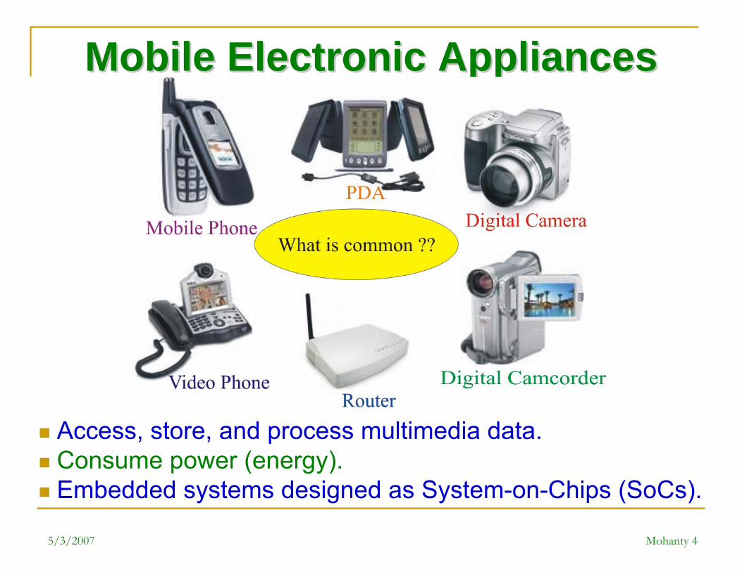
Mobile Electronic AppliancesMobile Electronic Appliances
Access, store, and process multimedia data.Consume power (energy).Embedded systems designed as System-on-Chips (SoCs).

5/3/2007 Mohanty 5
Security Requirements in Security Requirements in SoCsSoCs : : The Big PictureThe Big Picture
Content security is of our interest which will be handled through digital rights management (DRM) facility.

5/3/2007 Mohanty 6
DRM : DefinitionDRM : DefinitionDigital Rights Management (DRM) is a generic term that refers to any of several technologies used by publishers, creators, or owners to control access and usage of digital data.
Typically a DRM system:Protects intellectual property by encrypting the data so that it can only be accessed by authorized users.
and/orMarks the content with a digital watermark so that the content can not be freely distributed.

5/3/2007 Mohanty 7
DRM : Associated TechniquesDRM : Associated TechniquesWatermarking / Steganography: Embed additional data into a multimedia object visibly or invisibly.
Cryptography / Scrambling / Hashing: Transform multimedia data from plain form to another form using various functions.
… and many more … techniques.

5/3/2007 Mohanty 8
DRM : ExamplesDRM : ExamplesWatermarking
Cryptography
Judicious use of both encryption and watermarking necessary for multilayer protection through DRM.

5/3/2007 Mohanty 9
Our Solution for DRM:Our Solution for DRM:Secure Digital Camera (SDC)Secure Digital Camera (SDC)

5/3/2007 Mohanty 10
Secure Digital CameraSecure Digital CameraAn apparatus built as system-on-a-chip (SoC) with standards features of digital camera and built in facility for real-time, low-cost, low-power DRM.
For a given image/video SDC needs to prove:Copyright (visible watermarking)Extent of tampering (invisible-fragile watermarking)Source of image i.e. camera information, place, or date (invisible-robust or visible watermarking)Owner’s, creator's, or cameraman’s information (invisible-robust or visible watermarking)…….. and more.

5/3/2007 Mohanty 11
Proposed Secure Digital CameraProposed Secure Digital Camera(System(System--onon--aa--Chip : Chip : SoCSoC))
ControlData

5/3/2007 Mohanty 12
Hardware Based DRM : AdvantagesHardware Based DRM : AdvantagesEasy integration with multimedia hardware, such as digital camera, network processor, GPU, etc.Low-power consumption compared to software.High-performance compared to software.Higher reliability and availability compared to software. More useful for real-time applications like digital video broadcasting.Low-cost compared to having explicit software.DRM right at the source end will ensure that the information is always protected.DRM integrated with multimedia creating component will be more acceptable as legal evidence.

5/3/2007 Mohanty 13
SystemSystem--onon--aa--ChipChipDesign Challenges for Design Challenges for
Security, Power, and Security, Power, and Performance TradeoffsPerformance Tradeoffs

5/3/2007 Mohanty 14
Secure Secure SoCSoC Design Space ExplorationDesign Space Exploration
• Multidimensional design space, 3 are shown.
• More the security processing more the energy consumption and slower the performance.

5/3/2007 Mohanty 15
Different Forms of Attacks on Different Forms of Attacks on SoCsSoCs

5/3/2007 Mohanty 16
Power Dissipation in Power Dissipation in NanoNano--CMOS CMOS Based SystemsBased SystemsPower DissipationPower Dissipation
Static DynamicSubthreshold LeakageGate Leakage
Reverse-biased diode Leakage
Capacitive Switching Current
Short Circuit CurrentTransient Gate Leakage
• Almost the entire consumer electronic industry today is driven by nano-CMOS technology.
• Their low-power design is necessary to: reduce energy and cooling costs, to increase battery life, and more.

5/3/2007 Mohanty 17
Secure Secure SoCSoC Design : Two ModesDesign : Two ModesAddition of DRM features in SoC:
AlgorithmsProtocolsArchitecturesAccelerators / Engines
Consideration of DRM as a dimension in the design flow:
New design methodologyDesign automation or computer aided design (CAD) tools for fast design space exploration.

5/3/2007 Mohanty 18
Secure Digital Camera : Secure Digital Camera : AMSAMS--SoCSoC Research ChallengesResearch Challenges
Development of hardware amenable algorithms.
Building efficient VLSI architectures.
Hardware-software co-design for security, power, and performance tradeoffs.
Analog mixed-signal system-on-a-chip (AMS-SoC) design for security, power, and performance tradeoffs.

5/3/2007 Mohanty 19
AnalogAnalog--Digital MixedDigital Mixed--Signal DesignSignal DesignA side channel attack is any attack based on information gained from the physical implementation of an encryption system.
Static CMOS based circuit implementation are vulnerable to such attacks.
Vulnerable to side channel attack.
May abstract switching activity and reduce information leaking.

5/3/2007 Mohanty 20
HardwareHardware--Software CoSoftware Co--DesignDesignWith the same philosophy, hardware with embedded software based encryption system can be considered.
Vulnerable to side channel attack.
May abstract switching activity and reduce information leaking.

5/3/2007 Mohanty 21
SCMOS Logic and Differential Logic SCMOS Logic and Differential Logic Digital CircuitDigital Circuit
Develop logic styles and routing techniques such that power consumption per cycle is constant and capacitance charged at a node is constant.
Vulnerable to side channel attack.
May abstract switching activity and reduce information leaking.

5/3/2007 Mohanty 22
Secure Digital Camera : Secure Digital Camera : Different Design AlternativesDifferent Design Alternatives
New CMOS sensor with DRM.
New ADC with DRM.
Independent DRM (watermarking, encryption, etc.) processors.
DRM (watermarking, encryption, etc.) co-processor for DSP.
New instruction set architecture for RISC to support DRM at micro-architecture level.

5/3/2007 Mohanty 23
A LowA Low--Power Watermarking Power Watermarking Chip for the SDCChip for the SDC

5/3/2007 Mohanty 24
Our LowOur Low--Power Design Approach Power Design Approach
Adjust the frequency and supply voltage in a coordinated manner to reduce dynamic power while maintaining performance.
NOTE: We also have developed methods for gate-oxide and subthreshold leakage power reduction.

5/3/2007 Mohanty 25
Highlights of our Proposed Chip Highlights of our Proposed Chip
DCT domain processing.
First to insert both visible and invisible watermarks.
First low-power design for watermarking using dual voltage and dual frequency.
Uses pipelined and parallelization for better performance.
Uses decentralized controller scheme to indirectly implement clock gating for power reduction.

5/3/2007 Mohanty 26
Algorithms Selected for the ChipAlgorithms Selected for the ChipVisible watermarking algorithm:S. P. Mohanty, K. R. Ramakrishnan, and M. S. Kankanhalli, "A DCT Domain Visible Watermarking Technique for Images", in Proceedings of the IEEE International Conference on Multimedia and Expo, 2000, pp. 1029-1032.
Invisible watermarking algorithm:I. J. Cox, J. Kilian, T. Leighton, and T. Shamoon, “Secure Spread Spectrum Watermarking for Multimedia”, IEEE Transactions on Image Processing, Vol. 6, No. 12, 1997, pp. 1673-1687.
NOTE: Highest cited papers in respective category.
5/3/2007 Mohanty 27
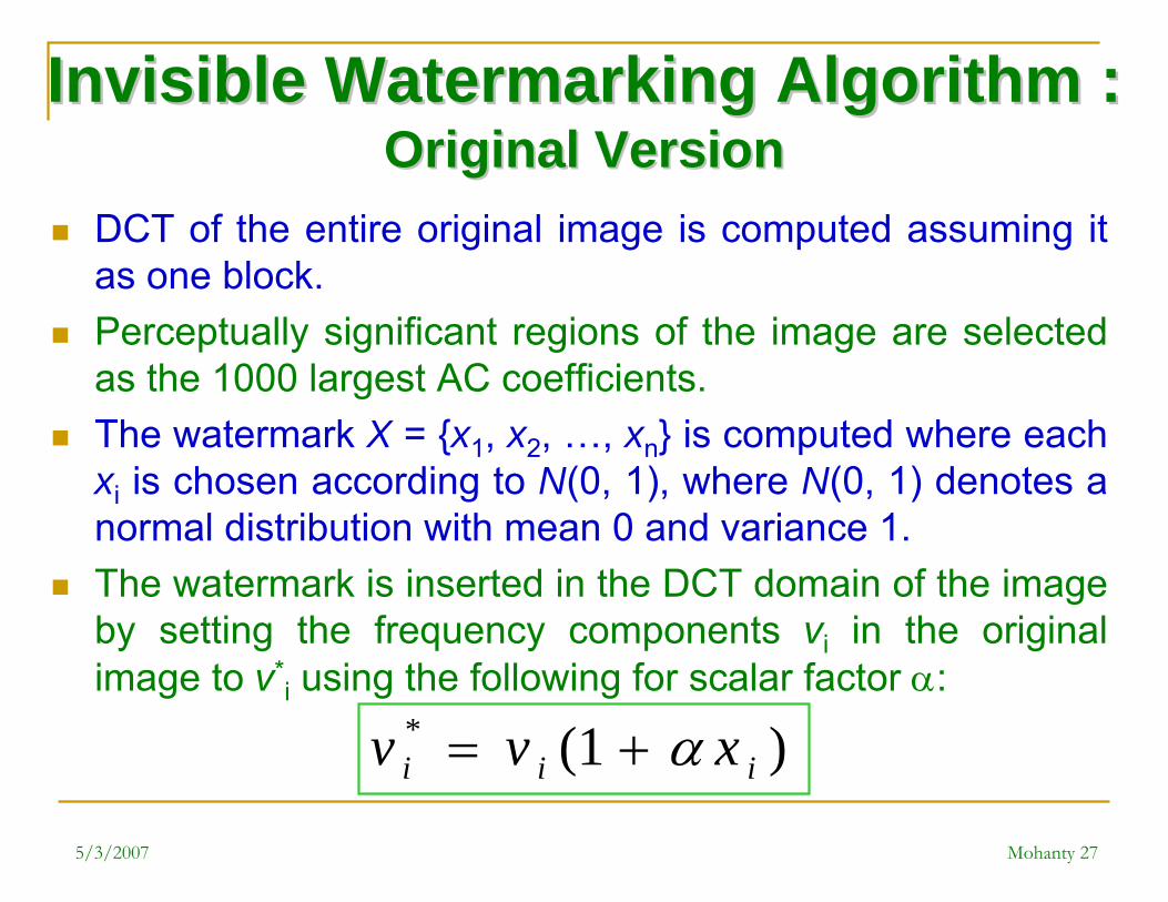
Invisible Watermarking Algorithm : Invisible Watermarking Algorithm : Original VersionOriginal Version
DCT of the entire original image is computed assuming it as one block.Perceptually significant regions of the image are selected as the 1000 largest AC coefficients.The watermark X = {x1, x2, …, xn} is computed where each xi is chosen according to N(0, 1), where N(0, 1) denotes a normal distribution with mean 0 and variance 1.The watermark is inserted in the DCT domain of the image by setting the frequency components vi in the original image to v*
i using the following for scalar factor α:
)1(*iii xvv α+=

5/3/2007 Mohanty 28
Invisible Watermarking Algorithm : Invisible Watermarking Algorithm : Modified VersionModified Version
1. Divide the original image into blocks.
2. Calculate the DCT coefficients of all the image blocks.
3. Generate random numbers to use as watermark.
4. Consider the 3 largest AC-DCT coefficients of an image block for watermark insertion.

5/3/2007 Mohanty 29
Visible Watermarking AlgorithmVisible Watermarking Algorithm
1. Divide original and watermark image into blocks.
2. Calculate DCT coefficients of all the blocks.
3. Determine the blocks containing edges in the original image.
4. Find the local and global statistics (μ, σ) of original image using DC-DCT and AC-DCT coefficients.
5. Calculate the scaling and embedding factors.
6. Add the original image DCT coefficients and the watermark DCT coefficients block by block.

5/3/2007 Mohanty 30
Visible Watermarking Algorithm Visible Watermarking Algorithm ……The αk and βk for edge blocks are taken to be αmax and βmin, respectively.
For non-edge blocks αk and βk are computed as:
αk and βk are then scaled to the ranges (αmin, αmax) and (βmin , βmax), respectively.
{ }[ ]{ }[ ]2**
*
2***
)(exp11
)(exp
IDCDCAC
k
IDCDCACk
Ik
Ik
IkIk
μμσ
β
μμσα
−−−=
−−=

5/3/2007 Mohanty 31
Visible Watermarking Algorithm : Visible Watermarking Algorithm : ModificationsModifications
Use cIwhite(0,0) for normalization instead of cImax(0,0).Rewrite αk and βk equations: { }[ ]
{ }[ ]2**
2**
)(exp1
)(exp
Im
Im
IIk
Ik
ax
IIk
ax
Ik
DCDCAC
ACk
DCDCAC
ACk
μμσ
σβ
μμσσ
α
−−−=
−−=
Remove σACImax:{ }[ ]
{ }[ ]2**
2**
)(exp11
)(exp
IDCDCAC
kc
IDCDCACkc
Ik
Ik
IkIk
μμσ
β
μμσα
−−−=
−−=
{ }{ }4**2**
4**2**
)()(1
)()(1
IDCDCIDCDCAC
kc
IDCDCIDCDCACkc
IkIk
Ik
IkIkIk
μμμμσ
β
μμμμσα
−−−=
−+−−=
Remove exponential using Taylor series:
Scale to the ranges (αmin, αmax) and (βmin, βmax), respectively.

5/3/2007 Mohanty 32
The Proposed ArchitectureThe Proposed Architecture

5/3/2007 Mohanty 33
The Proposed Architecture : The Proposed Architecture : Pipeline and Parallelism Pipeline and Parallelism
• The visible architecture has 3 stage pipeline and the invisible architecture has 2 stage pipeline.

5/3/2007 Mohanty 34
The Proposed Architecture : The Proposed Architecture : Dual Voltage and FrequencyDual Voltage and Frequency

5/3/2007 Mohanty 35
Dual Voltage : Level ConvertersDual Voltage : Level ConvertersLevel converters are required to step up the low voltage to high voltage.Single supply level converter is used as it is faster and consumes less power for its operation.

5/3/2007 Mohanty 36
Prototype Chip : LayoutPrototype Chip : Layout
NOTE: Standard cell design style adopted. Low-power cells are created based on Virginia Tech: TSMC 0.25µm library.

5/3/2007 Mohanty 37
Prototype Chip: StatisticsPrototype Chip: Statistics
Technology: TSMC 0.25µmTotal Area : 16.2 sq-mmDual Clocks: 284MHz and 71MHzDual Voltages: 2.5V and 1.5VNo. of Transistors: 1.4millionPower Consumption: 0.3mW
NOTE: Lowest power consuming watermarking chip available at present.
5/3/2007 Mohanty 38
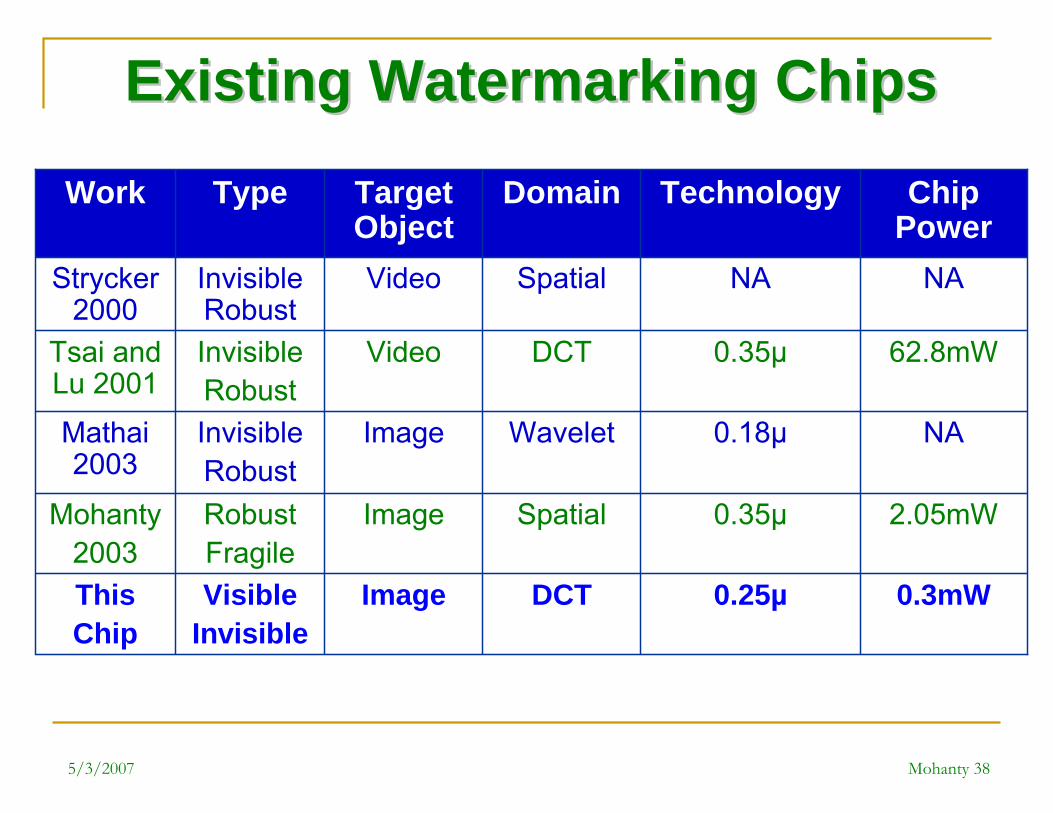
Existing Watermarking ChipsExisting Watermarking Chips
0.3mW0.25µDCTImageVisibleInvisible
ThisChip
2.05mW0.35µSpatialImageRobustFragile
Mohanty2003
NA0.18µWaveletImageInvisibleRobust
Mathai2003
62.8mW0.35µDCTVideoInvisibleRobust
Tsai and Lu 2001
NANASpatialVideoInvisible Robust
Strycker2000
Chip Power
TechnologyDomainTarget Object
TypeWork

5/3/2007 Mohanty 39
Secure Digital Camera (SDC): Secure Digital Camera (SDC): Some Application ScenariosSome Application Scenarios

5/3/2007 Mohanty 40
Application: Copyright ProtectionApplication: Copyright ProtectionPublicly available imagesDigital LibraryDVD VideoDigital TV Broadcasting
NOTE: Can enhance revenue of movie/broadcasting industry.
5/3/2007 Mohanty 41
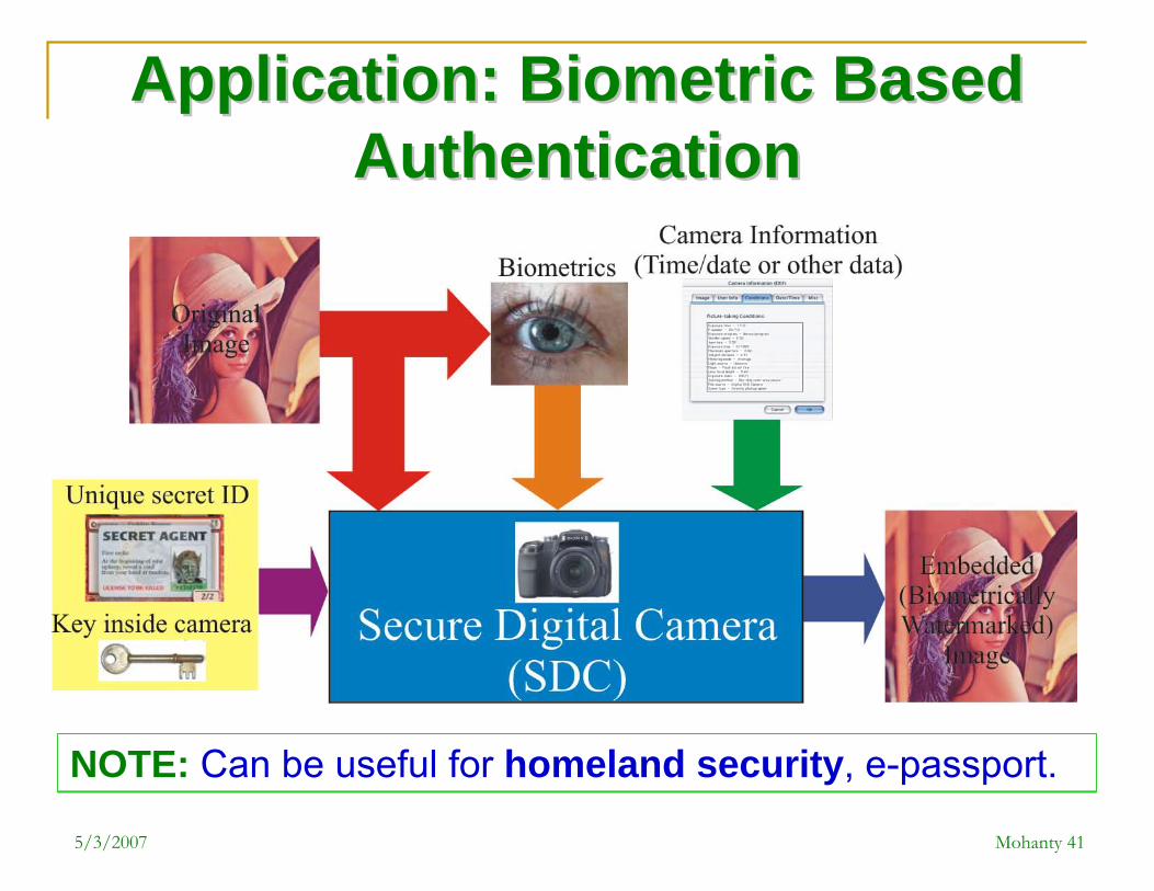
Application: Biometric Based Application: Biometric Based AuthenticationAuthentication
NOTE: Can be useful for homeland security, e-passport.

5/3/2007 Mohanty 42
Our Ongoing ResearchOur Ongoing Researchin Mixedin Mixed--Signal CircuitsSignal Circuits

5/3/2007 Mohanty 43
Universal Voltage Level ConverterUniversal Voltage Level Converter
Single circuit performing 4 operations:−Step-up−Step-down−Pass signal−Block signal
Goals:−Power efficient design with minimal
number of transistors.−Minimal dynamic, subthreshold, and
gate-oxide leakage power.
Applications:−Multi-VDD based AMS-SoCs.

5/3/2007 Mohanty 44
Universal Voltage Level Converter Universal Voltage Level Converter ……
Input
Output
Select
Signal
11: Up 01: Down 10: Pass 11: Block
S0
S1

5/3/2007 Mohanty 45
Universal Voltage Level Converter Universal Voltage Level Converter ……
• gpdk_90nm technology from Cadence.
• Works under varying load from 1fF -200fF and at low voltages as 0.6V.
• Consumes power of 24.8 μW.
5/3/2007 Mohanty 46
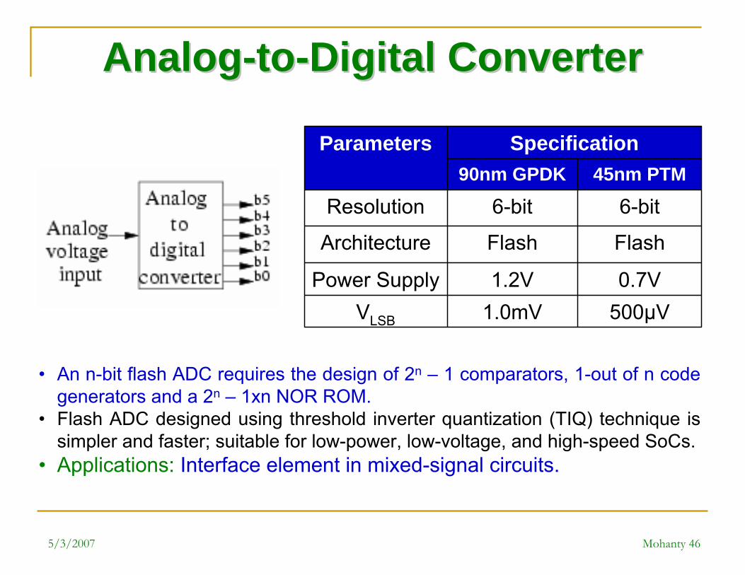
AnalogAnalog--toto--Digital ConverterDigital Converter
Specification
1.0mV1.2V
Flash
6-bit90nm GPDK
500µVVLSB
0.7VPower Supply
FlashArchitecture
6-bitResolution45nm PTM
Parameters
• An n-bit flash ADC requires the design of 2n – 1 comparators, 1-out of n code generators and a 2n – 1xn NOR ROM.
• Flash ADC designed using threshold inverter quantization (TIQ) technique is simpler and faster; suitable for low-power, low-voltage, and high-speed SoCs.
• Applications: Interface element in mixed-signal circuits.

5/3/2007 Mohanty 47
AnalogAnalog--toto--Digital Converter Digital Converter ……A 3-bit example
ComparatorsCode generator
ROM
PowerAvg
PowerPeak
SNDR
INL
DNL
Speed
45nm PTM90nm GPDK
Characterization
8.8µW 3.87W
45.42µW 4.87mW
31.9dB30.4dB
0.46LSB0.34LSB
0.7LSB0.47LSB
1Gs/sec1Gs/sec
Goals:─ Process-variation tolerant ADC.

5/3/2007 Mohanty 48
Voltage Controlled OscillatorVoltage Controlled Oscillator
VCO with frequency divider Output waveforms of the VCO and digital and analog frequency divider.
• It is seen that there is a 10% difference in the simulation results, depending on whether the frequency divider is considered as analog or digital.
• It is observed that 80% of the capacitive load is due to gate oxide tunneling and only 20% due to traditional gate capacitance when simulated for 45nm PTM.

5/3/2007 Mohanty 49
Secure Digital Pixel SensorsSecure Digital Pixel Sensors
Spatial-domain pixel-wise watermarking schemes will have less computational overhead.Additional circuitry will have minimal power dissipation overhead.Goal: Simulation and Optimization approaches for fast and accurate AMS-SoC design space exploration.

5/3/2007 Mohanty 50
ConclusionsConclusions

5/3/2007 Mohanty 51
SummarySummaryA low-cost, low-power camera is introduced that can perform DRM in real time.Hardware assisted DRM has several advantages over software only.Structure of SoCs that will realize the secure digital camera is an ongoing research.A low-power watermarking chip is designed that consumes 0.3mW power.SDC to be realized as an SoC will involve security, power, and performance tradeoffs.Design automation or computer-aided design (CAD) tools would be necessary for fast and automatic AMS-SoC design space exploration.

5/3/2007 Mohanty 52
ReferencesReferencesS. P. Mohanty, et al., "VLSI Architecture of an Invisible Watermarking Unit for a Biometric-Based Security System in a Digital Camera," in Proceedings of the 25th IEEE International Conference on Consumer Electronics (ICCE), 2007.
O. B. Adamo, S. P. Mohanty, E. Kougianos, and M. Varanasi, “VLSI Architecture for Encryption and Watermarking Units Towards the Making of a Secure Digital Camera,” in Proceedings of the IEEE International SOC Conference (SOCC), pp. 141-144, 2006.
S. P. Mohanty, et al., “A Dual Voltage-Frequency VLSI Chip for Image Watermarking in DCT Domain,” IEEE Transactions on Circuits and Systems II (TCAS-II), Vol. 53, No. 5, May 2006, pp. 394-398.
N. M. Kosaraju, M. Varanasi, and S. P. Mohanty, “A High-Performance VLSI Architecture for Advanced Encryption Standard (AES) Algorithm,”in Proceedings of the 19th IEEE International Conference on VLSI Design (VLSID), pp. 481-484, 2006.

5/3/2007 Mohanty 53
References References ……S. Ravi, A. Raghunathan, P. Kocher, S. Hattangady, “Security in Embedded Systems: Design Challenges,” ACM Transactions on Embedded Computing Systems (TECS), Volume 3 , Issue 3, August 2004, pp. 461 – 491.
S. P. Mohanty, et al., “A VLSI Architecture for Visible Watermarking in a Secure Still Digital Camera (S2DC) Design,” IEEE Transactions on VLSI Systems (TVLSI), Vol. 13, No. 8, Aug 2005, pp. 1002-1012.
G. R. Nelson, et al., “CMOS Image Sensor with Watermarking Capabilities,” in Proceedings of the IEEE International Symposium on Circuits and Systems (ISCAS), 2005, pp. 5326-5329.
P. Blythe and J. Fridrich, “Secure Digital Camera,” in Proceedings of Digital Forensic Research Workshop (DFRWS), 2004.
R. Puri et. al., “Pushing ASIC Performance in a Power Envelope,” in the Proceedings of the Design Automation Conference (DAC), 2003, pp. 788-793.

5/3/2007 Mohanty 54
References References ……S. P. Mohanty, N. Ranganathan, and R. K. Namballa, “VLSI Implementation of Invisible Digital Watermarking Algorithms Towards the Development of a Secure JPEG Encoder,” in the Proceedings of the IEEE Workshop on Signal Processing System, pp. 183-188, 2003.
D. Hwang, K. Tiri, A. Hodjat, B.C. Lai, S. Yang, P. Schaumont, I. Verbauwhede, "A AES-Based Security Coprocessor IC in 0.18-μm CMOS with Resistance to Differential Power Analysis Side-Channel Attacks”, IEEE Journal of Solid-State Circuits (JSSC), vol.44, issue 4, pp.781-792, 2006.
K. Tiri, and I. Verbauwhede, "A Digital Design Flow for Secure Integrated Circuits,” IEEE Transactions on Computer-Aided Design of Integrated Circuits and Systems (TCAD), vol.25, no.7, pp.1197-1208, 2006.
http://www.iprsystems.com, http://www.eifonline.org, http://www.trl.ibm.com/projects/RightsManagement/datahiding/index_e.htm,http://www.ctr.columbia.edu/~cylin/vismark/vismark.html, and more web sites ….

5/3/2007 Mohanty 55
For more information:For more information:http://www.cse.unt.edu/~smohantyhttp://www.cse.unt.edu/~smohanty