close supply chain collaboration enables easy...
TRANSCRIPT

AT & S Austria Technologie & Systemtechnik Aktiengesellschaft | Fabriksgasse13 | A-8700 Leoben Tel +43 (0) 3842 200-0 | E-Mail [email protected]
www.ats.net
Close supply chain collaboration enables easy implementation of
chip embedded power SiP
Gerald Weidinger, R&D Project Leader, AT&S

Embedding Technology Industrialization
History of embedded Die Technology
2000 2002 2004 2006 2008 2010 2012 2014 2016
Printed resistor
Printed capacitor
Discrete resistor
Discrete capacitor
Embedded silicon
1970
Concepts Development Projects Industrialization Serial Production Research
Embedded Chip

Embedding Technology Industrialization
Die FET FET
R, L, C
2

Why Chip Embedding?
AT&S Confidential - NDA Restrictions Apply AT&S Advanced Packaging
Unique Selling Propositions … in detail
Miniaturization • Footprint reduction • Higher component integration (additional assembly layer)
Electrical performance • Improved signal performance (higher data rates) • Reduction of parasitic effects
Mechanical performance
• Higher durability and reliability through copper-to-copper connections (copper filled microvias)
• Package enables protective enclosure • High drop, shock and vibration tolerance
Thermal management • Improved heat dissipation through direct copper connection • Improved heat dissipation FR4 versus air (compared to SMD)
Additional functions Reduction of overall cost EMI shielding
• EMV shielding (partial or full shielding of a package) • Package is the housing no additional molding required
ECP is supporting the trend towards modularization
• Lower set-up costs compared to other packaging technologies (packaging versus PCB processes)
• Customization of footprint and module versions can be done due to digital imaging - no separate tooling necessary (e.g. QFN)
Anti-Tamper and Security • Hidden electronics preventing reverse engineering and
counterfeiting

Embedding Technology Industrialization
Our collaboration enables customers success
• Global footprint • Strong R&D focus • High volume
manufacturing experience , capacity and capability
• Brought product portfolio
• Strong customer base • Long history in
embedded technology
• Global footprint • High volume
manufacturing experience , capacity and capability
• Excellent testing capabilities
• Strong customer base • Brought experience in
backend processing of various applications
Alignment on • Business processes • Aligned technical
capabilities • Common focus on
segments and applications

Supply Chain Offering
Strategic supply chain collaboration is a key success factor
Co- Design
Wafer to Die
Substrate embedded chip
Package assembly
Test
SMT Top FC / under fill
Cap or Mold Solder Ball Attach
Package saw
KGD test RDL
Thin / Dice Inspect / TnR
Substrate manufacturing Embedded chip
Strip Test
Package level test Reliability test
Alignment on Design Rules & Roadmaps - Substrate design - Assembly design
- Design integration
Customer Specs
Customer Consigned Option
April 2015 - Joint marketing / supply chain agreement
Between AT&S and UTAC for 3D SiP with embedded chip
technology. Collaboration press release April 2016.
AT&S over 5 years production embedding experience.
CMOS driver
Cbyp
GaAs FET die
other passive Components SMT

UTAC at a glance
6
• Outsourced Semiconductor Assembly and Test services (OSAT) provider in
support of Analog, Mixed-Signal, Logic, Power and Memory products.
• UTAC 2015 Revenue $878M; Ranked 6th in the Top Ten OSATs
• Focus – Assy, Test and Full Turnkey; Test comprises 35% of sales in 2015.
• 1997 Established in Singapore
• Mfg Footprint - Singapore, Taiwan, Malaysia, Indonesia, Thailand, China.
• >260K M2 Manufacturing Space and ~ 12K Employees Globally.
• Sales offices located worldwide.
• Markets: Mobile Phone, Automotive, Security, Wearable’s, Industrial & Medical.
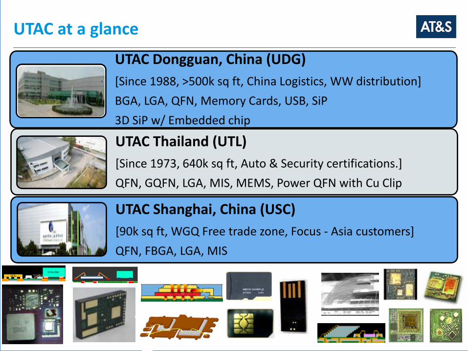
UTAC at a glance
7
UTAC Thailand (UTL)
[Since 1973, 640k sq ft, Auto & Security certifications.]
QFN, GQFN, LGA, MIS, MEMS, Power QFN with Cu Clip
UTAC Shanghai, China (USC)
[90k sq ft, WGQ Free trade zone, Focus - Asia customers]
QFN, FBGA, LGA, MIS
UTAC Dongguan, China (UDG)
[Since 1988, >500k sq ft, China Logistics, WW distribution]
BGA, LGA, QFN, Memory Cards, USB, SiP
3D SiP w/ Embedded chip

High-End Interconnection
Solutions for
Mobile Devices, Automotive,
Industrial, Medical Applications
One of the
most profitable
Players in the
Industry: EBITDA margin of 22%
in FY 2015/16
Continuously
Outperforming
market growth
€ 762.9m Revenue in FY 2015/16,
5.2% organic growth
# 1 manufacturer in Europe
# 3 in High-End Technology
worldwide
9,165 employees
Cost-competitive production
footprint with
6 plants in Europe and Asia
8
AT&S – a world leading high-tech PCB company

AT&S at a glance & global footprint
BU AIM Headquarters Plant Leoben, Austria Headquarters Staff: ~ 950 Customer Orientation: 9% Automotive 91% Industrial
BU AIM Plant Fehring, Austria Staff: ~350 Customer Orientation: 44% Automotive 56% Industrial
BU MS Plant Shanghai, China Staff: ~4600 Customer Orientation: 84% Mobile Devices 14% Automotive 2% Industrial
BU AIM Plant Nanjangud, India Staff: ~1.100 Customer Orientation: 60% Automotive 40% Industrial
BU MS Plant Chongqing, China Staff: ~1800
AT&S AG Headquarters
Leoben, Austria
BU MS Headquarters
Hong Kong, China
AT&S AG Headquarters Sales Offices /Representations Business Unit Mobile Devices & Substrates (BU MS) Business Unit Industrial & Automotive (BU IA)
BU AIM Plant Ansan, Korea Staff: ~280 Customer Orientation: 13% Automotive 47% Industrial 40% Mobile Devices

ECP® Basics – What’s ECP®
AT&S ECP® - Embedded Component Packaging
ECP® (Embedded Component Packaging) uses the space in an organic, laminate substrate (Printed Circuit Board) for active and passive components integration
Components embedding into the PCB core with copper plated microvia connections

ECP® Basics – Keyfacts
AT&S ECP® - Embedded Component Packaging
Laser drilled microvias
Galvanic copper plating
HDI PCB processes
PCB material and processes
Various combination of stack-ups possible
Active and/or passive components
Copper surface on IO‘s
Thickness 100µm - 350µm
In development: 80 – 500µm
Miniaturization
Reliable interconnection
Performance
Protection of components

Product Illustrations
X-section of embedded devices
SMT CSP
PCB with embedded
IC
AT&S Confidential - NDA Restrictions Apply AT&S Advanced Packaging
18,3 µm
87,9 µm
Embedded passives
CT image of embedded caps in a 4 layer PTH board)
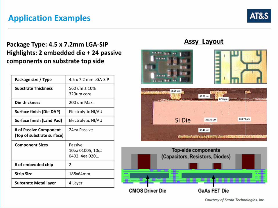
Application Examples
Package size / Type 4.5 x 7.2 mm LGA-SIP
Substrate Thickness 560 um ± 10% 320um core
Die thickness 200 um Max.
Surface finish (Die DAP) Electrolytic NI/AU
Surface finish (Land Pad) Electrolytic NI/AU
# of Passive Component (Top of substrate surface)
24ea Passive
Component Sizes Passive 10ea 01005, 10ea 0402, 4ea 0201.
# of embedded chip 2
Strip Size 188x64mm
Substrate Metal layer 4 Layer
Package Type: 4.5 x 7.2mm LGA-SIP Highlights: 2 embedded die + 24 passive components on substrate top side
Assy Layout
Si Die

UTAC & AT&S Collaboration
Summary
System in a package (SiP) is a strategic focus area for UTAC and AT&S
3D SiP with Embedded Chip provides integration, size and performance benefits over 2D planar SiP solutions
3D Embedded Chip technology adoption is accelerating in Power and High Density Interconnect Applications
Supply chain collaboration for emerging 3D SiP solutions with embedded chip technology will advanced the technology and provide full turnkey (FTK) supply solutions for customers.
Flexible business models available to fit to customer requirements
AT&S Confidential - NDA Restrictions Apply AT&S Advanced Packaging

AT & S Austria Technologie & Systemtechnik Aktiengesellschaft | Fabriksgasse13 | A-8700 Leoben Tel +43 (0) 3842 200-0 | E-mail [email protected]
www.ats.net
AT&S first choice for advanced applications