cmos integrated analog-to-digital and digital-to-analog …978-1-4757-376… · ·...
TRANSCRIPT
CMOS INTEGRATED ANALOG-TO-DIGITAL AND DIGITAL-TO-ANALOG CONVERTERS
2nd EDITION

mE KLUWER INTERNA TIONAL SERIES IN ENGINEERING AND COMPUTER SCIENCE
ANALOG CIRCUITS AND SIGNAL PROCESSING Consulting Editor: Mohammed Ismail. Ohio State University
RelaJed Titles:
SYSTEMATIC DESIGN OF ANALOG IP BLOCKS Vandenbussche and Gielen ISBN: 1-4020-7471-9
SYSTEMATIC DESIGN OF ANALOG IP BLOCKS Cheung & Luong ISBN: 1-4020-7466-2
LOW-VOLTAGE CMOS LOG COMPANDING ANALOG DESIGN Serra-Graells, Rueda & Huertas ISBN: 1-4020-7445-X
CIRCUIT DESIGN FOR WIRELESS COMMUNICATIONS Pun, Franca & Lerne ISBN: 1-4020-7415-8
DESIGN OF LOW-PHASE CMOS FRACTIONAL-N SYNTHESIZERS DeMuer & Steyaert ISBN: 1-4020-7387-9
MODULAR LOW-POWER, HIGH SPEED CMOS ANALOG-TO-DIGITAL CONVERTER FOR EMBEDDED SYSTEMS
Lin, Kemna & Hosticka ISBN: 1-4020-7380-1
DESIGN CRITERIA FOR LOW DISTORTION IN FEEDBACK OPAMP CIRCUITE Hemes & Saether ISBN: 1-4020-7356-9
CIRCUIT TECHNIQUES FOR LOW-VOLTAGE AND HIGH-SPEED AID CONVERTERS Walteri ISBN: 1-4020-7244-9
DESIGN OF IDGH-PERFORMANCE CMOS VOLTAGE CONTROLLED OSCILLATORS Dai and Harjani ISBN: 1-4020-7238-4
CMOS CIRCUIT DESIGN FOR RF SENSORS Gudnason and Bruun ISBN: 1-4020-7127-2
ARCHITECTURES FOR RF FREQUENCY SYNTHESIZERS Vaucher ISBN: 1-4020-7120-5
THE PIEZOJUNCTION EFFECT IN SILICON INTEGRA TED CIRCUITS AND SENSORS Pruett and Meijer ISBN: 1-4020-7053-5
CMOS CURRENT AMPLIFIERS; SPEED VERSUS NONLINEARITY Koli and Halonen ISBN: 1-4020-7045-4
MULTI-STANDARD CMOS WIRELESS RECEIVERS U and Ismail ISBN: 1-4020-7032-2
A DESIGN AND SYNTHESIS ENVIRONMENT FOR ANALOG INTEGRA TED CIRCUITS Van der PIas, Gielen and Sansen ISBN: 0-7923-7697-8
RF CMOS POWER AMPLIFIERS: THEORY, DESIGN AND IMPLEMENTATION Hella and Ismail ISBN: 0-7923-7628-5
DATA CONVERTERS FOR WIRELESS STANDARDS C. Shi and M. Ismail ISBN: 0-7923-7623-4
DIRECT CONVERSION RECEIVERS IN WIDE-BAND SYSTEMS A. Parssinen ISBN: 0-7923-7607-2
AUTOMATIC CALIBRATION OF MODULATED FREQUENCY SYNTHESIZERS D.McMahill ISBN: 0-7923-7589.{)
MODEL ENGINEERING IN MIXED-SIGNAL CIRCUIT DESIGN S. Huss ISBN: 0-7923-7598-X
ANALOG DESIGN FOR CMOS VLSI SYSTEMS F. Maloberti ISBN: 0-7923-7550-5

CMOS INTEGRATED ANALOG-TO-DIGITAL AND
DIGITAL-TO-ANALOG CONVERTERS
2nd Edition
by
Rudy van de Plassche Broadcom Netherlands BY, The Netherlands
and Broadcom, Irvine, CA, U.S.A.
SPRINGER SCIENCE+BUSINESS MEDIA, LLC
A C.I.P. Catalogue record for this book is available from the Library of Congress.
ISBN 978-1-4419-5367-4 ISBN 978-1-4757-3768-4 (eBook) DOI 10.1007/978-1-4757-3768-4
AU Rights Reserved © 2003 Springer Science+Business Media New York
Originally published by Kluwer Academic Publishers, Boston in 2003 Softcover reprint ofthe hardcover 2nd edition 2003
No part of this work may be reproduce<!. stored in a retrieval system, or transmitted in any form or by any means, electronic, mechanical, photocopying, microfilming, recording
or otherwise, without written permission from the Publisher, with the exception of any material supplied specifically for the purpose of being entered
and executed on a computer system, for exclusive use by the purchaser of the work.
Contents
List of figures
List of tables
List of symbols
Preface
1 The converter as a black box 1.1 Introduction................ 1.2 Basic D I A and AID converter function 1.3 Classification of signals. . . . . .
1.3.1 Different signal conditions . 1.3.2 Analog signals ...... . 1.3.3 Discrete-time signals ... . 1.3.4 Amplitude-discrete signals . 1.3.5 Digital signals. . . .
1.4 Quantization errors ..... 1.5 Oversampling of converters 1.6 Quantization error spectra . 1. 7 Amplitude dependence of quantization components 1.8 Multiple signal distortion ..... . 1.9 Accurate dynamic range calculation ....... . 1.10 Sampling time uncertainty ............. .
1.10.1 Reduction of ENOB by sampling clock jitter 1.11 Sampling clock time uncertainty 1.12 Conversion systems . . . . . . . .
1.12.1 Sampling with no-aliasing 1.12.2 Sampling with aliasing .. 1.12.3 Sampling of quantization errors.
xiii
xxvii
xxix
xxxv
1 1 2
5 5 5 6 6 6 7
10 12 16 17 19 21 23 25 27 28 29 29

11
1.13 Nyquist filtering in AID converter systems. 1.14 Combined analog and digital filter .... 1.15 Output filtering in D I A converter systems 1.16 Dynamic range and alias filter order . 1.17 Analog filter designs . . . . . . . . . .
1.17.1 Fourth order Butterworth filter 1.17.2 Fifth order Butterworth filter . 1.17.3 Digital filter design ...... .
1.18 Minimum required stop band attenuation 1.19 Conclusion ................ .
CONTENTS
31 32 34 41 42 42 43 45 45 48
2 Specifications of converters 51 51 52 53 55 57 57 57 58 62 64 64 65
2.1 Introduction ..... . 2.2 Digital data coding . . . . 2.3 Digital coding schemes . . 2.4 Ideal and Non-ideal converters 2.5 DC specifications . . . . .
2.5.1 Absolute accuracy ... 2.5.2 Relative accuracy. . . . 2.5.3 Nonlinearity calculation 2.5.4 Differential nonlinearity 2.5.5 Offset . . . . . . . . . . 2.5.6 Temperature dependence 2.5.7 Supply voltage . . . .
2.6 Dynamic specifications. . . . . . 65 2.6.1 Signal-to-Noise Ratio. . . 65 2.6.2 Spurious Free Dynamic Range 66 2.6.3 Effective Number Of Bits (ENOB's) 69 2.6.4 Dynamic range versus converter linearity 69 2.6.5 Required accuracy of converter elements. 70 2.6.6 Element matching versus INL of 8 to 14 bit converters 71 2.6.7 ENOB and SFDR versus INL converter model 75 2.6.8 Intermodulation modeling 79 2.6.9 Glitches............ 82 2.6.10 Noise ............ . 2.6.11 Minimum reference step size. 2.6.12 Bit Error Rate (BER) ... 2.6.13 Maximum sampling rate .. 2.6.14 Digital signal feed-through 2.6.15 Distortion . . . . . . . . . .
85 91 92 93 94 95
CONTENTS
2.6.16 Power supply rejection ratio . 2.6.17 Settling time .. 2.6.18 Acquisition time .. 2.6.19 Aperture time ... 2.6.20 Sample-to-hold step 2.6.21 Droop rate ..... 2.6.22 Signal feed-through during hold mode 2.6.23 Noise in sample-and-hold amplifiers 2.6.24 Overview of sample-and-hold specifications 2.6.25 Analog system bandwidth ...... . 2.6.26 Differential gain and differential phase
2.7 Figure of Merit 2.8 Conclusion ........ .
3 High-speed AID converters 3.1 Introduction ........ . 3.2 Design problems in high-speed converters
3.2.1 Timing errors ....... . 3.2.2 Distortion..........
3.3 Internal converter coding schemes . 3.3.1 Thermometer code 3.3.2 Gray encoder 3.3.3 Circular code . . .
3.4 Full-flash converters ... 3.4.1 Comparator input amplifier
3.5 Interpolation .. . . . . . . . . . . 3.5.1 DNL Improvement by interpolation 3.5.2 Multiple interpolation ... 3.5.3 Multiple interpolation error 3.5.4 Active interpolation . . 3.5.5 Capacitive interpolation . .
3.6 Averaging.............. 3.6.1 Averaging non-linearity error 3.6.2 Averaging non-linearity compensation 3.6.3 Moebius band averaging compensation . 3.6.4 Active averaging system . . . . . .
3.7 6-bit converter implementation . . . . . . 3.7.1 Differential input amplifier system 3.7.2 Second and third amplifier stages . 3.7.3 ENOB measurement of 6-bit converter.
iii
96 96 96 97 99 99
100 100 101 102 103 103 104
107 107 110 110 111 112 112 113 114 115 116 118 119 120 121 122 123 124 126 127 128 128 130 131 132 132

IV
3.7.4 Specification of 6-bit converter 3.8 Discrete time flash converter .
3.8.1 Second amplifier stage . 3.9 Gray code full flash converters 3.10 Circular code flash converters .
CONTENTS
134 134 137 138 142
3.11 Two-step flash converters ... 144 3.11.1 Two-step AID converter implementation. 145 3.11.2 Two-step capacitive MDAC AID converter 147
3.12 Sub ranging converter architecture . . . . . . . . . 148 3.12.1 8-bit Sub ranging converter implementation 150 3.12.2 Coarse comparator. . . . . . . 151 3.12.3 Fine comparator . . . . . . . . . . . . 152 3.12.4 Reference ladder construction. . . . . 152 3.12.5 Interleaved comparator flash converter 153 3.12.6 Interleaved comparator two-step AID converter. 154 3.12.7 lO-bit subrange converter 157 3.12.8 Coarse converter stage. 158 3.12.9 Fine converter stage . . 159 3.12.10 10-bit converter data. . 160
3.13 Pipeline converter architecture 160 3.13.1 Single bit per stage sub-converter architecture. 161 3.13.2 Multi-bit pipeline converter . . . . . . . 164 3.13.3 Sharing amplifiers in pipeline converters 166
3.14 Folding converter system. . . . . . . . . . . . 169 3.14.1 Current-folding AID converter system 170 3.14.2 7-bit current folding implementation 171 3.14.3 Improved current folding system . 172 3.14.4 Fine converter system . . . . . . . 173 3.14.5 High-frequency rounding problem. 174 3.14.6 Double folding system. . . . . . . 174 3.14.7 8-bit folding and interpolation converter 176 3.14.8 Transimpedance amplifier . . . . . . . . 177 3.14.9 Transimpedance amplifier circuit diagram 178 3.14.10 Resistive interpolation . 179 3.14.11 Comparator circuit. . . . . . . . . . . . . 179 3.14.12 Converter specifications . . . . . . . . . . 181 3.14.13 Distributed S/H folding and interpolation converter 181 3.14.14 Distributed T IH folding and interpolation converter
architecture. . . . . . . . . . . . . . . . 183 3.14.15 Track-and-hold circuit implementation ......... 184

CONTENTS v
3.14.16 Cascaded folding block architecture 185 3.14.17 Triple folding block circuit diagram. 187 3.14.18 Coarse code generation ....... 188 3.14.19 Measurements ............ 188 3.14.208-bit distributed T /H folding and interpolation con-
verter specifications .......... 188 3.14.211O-bit folding and averaging converter 190 3.14.22 Improved averaging ........ 190 3.14.23 Drain load current sources. . . . . 192 3.14.24 Differential converter input system 193 3.14.25 Comparator circuit diagram. 194 3.14.26 Measurements ........ 195 3.14.2710-bit converter specifications
3.15 Time interleaved high-speed converters. 3.16 Minimum supply voltage calculation 3.17 Reference ladder signal feedthrough . 3.18 Bubble correction ...... . 3.19 Delay over interconnect lines 3.20 Conclusion ........ .
195 195 198 199 200 201 203
4 High-speed D / A converters 205 4.1 Introduction................. 205 4.2 High-speed D / A converter architectures . 205
4.2.1 Binary weighted converter coding. 206 4.2.2 Fully segmented converter architecture. 206 4.2.3 Partially segmentation combined with binary weight-
ing converter architecture . . . . . 206 4.3 Voltage weighting based architecture . . . . . 208
4.3.1 Dual-ladder lO-bit D / A converter. . . 208 4.3.2 Equal currents output ladder network 212 4.3.3 Data interleaved D / A converter . . . . 213
4.4 High-speed segmented converter architecture 214 4.4.1 10-bit 500 Msamples/sec digital-to-analog converter 216 4.4.2 Measurement results of 500 Msamples/s lO-bit converter219 4.4.3 A 10-bit 1-Gsample/s Nyquist digital-to-analog con-
verter . . . . . . . . . . . 221 4.4.4 Current matrix floor plan . . . . . . . . . . . . . . . . 222 4.4.5 Switch and latch circuit . . . . . . . . . . . . . . . . . 222 4.4.6 Measurement results of 1-Gsample/s lO-bit converter. 223 4.4.7 12-bit 500 Msample/s digital-to-analog converter ... 224

VI CONTENTS
4.4.8 Measurement results of the 12-bit 500 Msamplels digital-to-analog converter . . . . . . . . . . . . . . . . . . . . 225
4.4.9 Influence of wire delay on high-frequency performance 225 4.4.10 Digital-to-analog converter switching network model 227 4.4.11 SFDR and delay calculation model . . . . . . . . . . . 229 4.4.12 Output impedance of current cells ........... 231 4.4.13 Calculation of minimum current cell output impedance 233
4.5 Conclusion ............................ 234
5 High-resolution AID converters 5.1 Introduction .......... . 5.2 5.3 5.4
5.5
5.6 5.7 5.8 5.9
Single slope AID converter system Dual-slope AID converter system. Dual-ramp single-slope AID converter system 5.4.1 Accuracy analysis of the dual ramp AID converter Successive approximation converter system ....... . 5.5.1 Successive approximation AID converter examples 5.5.2 Digital-to-analog converter ............ . 5.5.3 Current subtraction circuit ............ . 5.5.4 Micropower successive approximation AID converter. 5.5.5 Current subtracter I comparator circuit diagram . . . . 5.5.6 12-bit switched capacitor successive approximation con-
verter .................. . Algorithmic AID converter .......... . Cyclic Redundant Signed Digit AID converter Self-calibrating capacitor AID converter Conclusion ............... .
6 High-resolution D I A converters 6.1 Introduction ............... . 6.2 Pulse-width modulation D I A converters 6.3 Integrating D I A converters . . . . . . . 6.4 Current weighting using ladder networks.
6.4.1 R-2R ladder network ....... . 6.4.2 MOS only binary weighted current network 6.4.3 MOS R-2R implementation . . . . . 6.4.4 4-bit R-2R MOS converter example . 6.4.5 Two-step current division network .. 6.4.6 MOS ladder network converter system 6.4.7 Weighted capacitor converter system .
237 237 238 240 241 243 244 246 246 247 248 250
251 254 256 260 262
263 263 264 266 270 270 271 273 274 275 276 277

CONTENTS vii
6.4.8 Weighted capacitor network with output amplifier . . 278 6.4.9 Weighted capacitor network with resistive interpolation279
6.5 Monotonic by design network systems 280 6.5.1 Voltage division operation . . . . . . . . 281 6.5.2 Current weighting operation. . . . . . . 283 6.5.3 MOS only monotonic by design system. 284 6.5.4 Active division MOS only monotonic by design system 285 6.5.5 Current-to-voltage converter 286
6.6 Self calibrating D / A converter system 287 6.7 Dynamic Element Matching . . . . . . 289
6.7.1 Basic dynamic divider scheme. 289 6.7.2 Practical dynamic divider circuit 292 6.7.3 Two-bit dynamic current divider scheme. 293 6.7.4 Dynamic current mirror circuit . . . . . . 296 6.7.5 Binary-weighted accurate current network 297 6.7.6 Binary-weighted current network with divided inter-
changing clock . . . . . . . . . . . . . . . . . . . . . . 298 6.7.7 Binary-weighted current network using equal inter-
changing clock frequencies . . . 299 6.7.8 16-bit binary network example . . . 299 6.7.9 Filtering and switching ....... 300 6.7.10 Randomizer to avoid ripple filtering 301
6.8 Current calibration principle ........ 302 6.8.1 Improved current calibration principle 305 6.8.2 Continuous current calibration system 306 6.8.3 Practical current calibration implementation 306 6.8.4 16-bit D / A converter system . . . . 307 6.8.5 Integral nonlinearity measurement 309 6.8.6 Dynamic performance measurement 309 6.8.7 D / A converter specifications 310 6.8.8 Some remarks about the ladder converter systems 310
6.9 Conclusion .......................... 311
7 Sample-and-hold amplifiers 7.1 Introduction ............. . 7.2 Basic sample-and-hold configuration
7.2.1 Signal bandwidth .... 7.2.2 7.2.3 7.2.4
Acquisition time . . . . . . . Aperture time accuracy . . . Sampling moment distortion calculation
313 313 314 314 315 316 317

viii CONTENTS
7.3
7.4 7.5 7.6
7.2.5 Differential sample-and-hold circuit ..... . 7.2.6 Sample clock bootstrapping . . . . . . . . . . 7.2.7 Differential sampling clock bootstrap circuit. 7.2.8 Low signal feedthrough switch .... 7.2.9 Time interleaved sample-and-hold .. 7.2.10 Signal dependent clock bootstrapping 7.2.11 Simple signal clock bootstrap system. 7.2.12 Modified signal clock bootstrap system. 7.2.13 Gate and bulk bootstrapping system 7.2.14 Double sided bootstrapping. 7.2.15 Sample and hold mode errors .. 7.2.16 MOS switch charge injection .. 7.2.17 Noise in sample-and-hold circuits Generalized non-inverting configurations 7.3.1 Double-buffered sample-and-hold circuit 7.3.2 Feedback improved sample-and-hold circuit 7.3.3 Integrating sample-and-hold circuit .... . 7.3.4 Practical integrating SIR circuit ..... . 7.3.5 Switched capacitor sample-and-hold circuit 7.3.6 Switched capacitor sample-and-hold circuit with gain. 7.3.7 CMOS non-inverting mode SIR example .... 7.3.8 MOS differential sample-and-hold. . . . . . . . 7.3.9 Sample-and-hold amplifier with full hold time . Inverting sample-and-hold circuit . . . . . . . . . . . . Operational range of simple sample-and-hold amplifiers Conclusion ......... .
8 Noise-shaping D / A conversion 8.1 Introduction ..................... . 8.2 Digital oversampling filtering ........... .
8.2.1 Combined digital-analog DI A output filter 8.2.2 Digital filter configuration 8.2.3 Quantization errors. . . . . . . . . .
8.3 Noise-shaping................. 8.3.1 Single bit digital-to-analog converter 8.3.2 Multi-bit digital-to-analog converter 8.3.3 8.3.4 8.3.5 8.3.6
First-order noise-shaper Second-order noise-shaper ..... . Third-order noise-shaper. . . . . . . Fourth-, fifth-, and sixth-order noise-shaper
318 320 321 322 323 324 324 326 326 327 328 329 333 335 335 336 336 337 338 339 340 342 344 345 346 347
349 349 350 351 352 353 353 355 356 357 360 361 364

CONTENTS
8.3.7 Largely oversampled noise-shaper . . 8.4 Multi-bit largely oversampled noise-shaper . 8.5 Stability analysis of noise-shapers . . . . . .
8.5.1 Noise-shaper stability model ..... 8.5.2 Root Locus stability analysis method. 8.5.3 First-order system ........ . 8.5.4 Second-order system . . . . . . . . 8.5.5 Simulation of second order system 8.5.6 Third-order system ........ . 8.5.7 Quantizer describing function model 8.5.8 Maximum global gain calculation .. 8.5.9 Extended quantizer model ..... .
ix
369 370 371 372 373 374 374 375 375 379 383 384
8.5.10 Root locus of second order system using extended quantizer model . . . . . . . . . . . . . . . . . . . . . . . . 387
8.5.11 Third order I-bit system using the extended quantizer model. . . . . . . . . . . . . . . 388
8.5.12 Multi-bit system analysis . . . . 389 8.6 Practical noise-shaping D / A converters. 391
8.6.1 16-bit D/A converter system .. 391 8.6.2 18-bit D / A converter system .. 395 8.6.3 Continuous time FIR reconstruction filter D / A converter 398 8.6.4 Combined digital-analog FIR filter architecture 399 8.6.5 FIR filter response . . . 400 8.6.6 Total filter response ..... . 8.6.7 Converter specification . . . . .
8.7 Multi-bit noise-shaping D / A converter 8.7.1 8.7.2 8.7.3 8.7.4 8.7.5
8.7.6 8.7.7 8.7.8 8.7.9 8.7.10 8.7.11 8.7.12
Multi-bit system configuration Detail of sign-magnitude converter Sign-magnitude self-calibration system . Total system implementation . . . . . . Multi-bit digital-to-analog converter using randomized Dynamic Element Matching . . . . . . . Non-filtered DEM D / A architecture . . Resistive element DEM D / A converter . Randomizer system .......... . Super audio 24-bit D / A converter .. . 15-level capacitive DEM D / A converter Differential dual 31-level DEM D/A converter. Third order noise-shaper architecture .....
402 402 403 403 405 405 406
407 408 409 410 410 411 412 413
x CONTENTS
8.7.13 Comparison between conventional DWA and partial DWA system architecture . . . . . 413
8.7.14 24-bit DI A converter performance 413 8.8 Conclusion ................. 415
9 Sigma-delta AID conversion 417 9.1 Introduction................... 417 9.2 General form of Sigma-delta AID converters. 418
9.2.1 Dynamic range . . . . . . . . . . . 422 9.3 General filter architectures. . . . . . . . . . . 423
9.3.1 I-bit Sigma-delta signal examples. . . 425 9.3.2 Multi-bit Sigma-delta signal examples 426 9.3.3 Return-to-zero D I A pulse . . . . . . . 427 9.3.4 Continuous time filter first order converter 428 9.3.5 Fully continuous time first order converter . 430
9.4 Discussion of basic converter architectures 432 9.4.1 First-order AID converter. . 432 9.4.2 Second-order AID converter. . . . 433 9.4.3 Third-order AID converter .... 435
9.5 Multi-stage sigma-delta converter (MASH) 437 9.6 Quantizer overload avoidance . . . . . . . . 438
9.6.1 Interstage gain scaling in cascaded converters 439 9.6.2 Local feedback system across individual integrators. 440 9.6.3 Gain scaling and local feedback in cascaded converters 440
9.7 Converter input circuitry ...... 441 9.7.1 Cross-coupled input sampling. 443 9.7.2 Clock timing scheme. . . . . . 444 9.7.3 Shared capacitor input circuit . 444
9.8 Practical 16-bit cascaded converter . 445 9.8.1 Converter specifications . . . 445
9.9 Feed-forward AID converter system 445 9.9.1 Continuous time input circuit 448 9.9.2 Intermediate stage circuit diagram 450 9.9.3 Simulated noise transfer function 451
9.10 Nth-order sigma-delta architecture . . 451 9.11 Bandpass sigma-delta converters .... 454 9.12 Low-pass to band-pass transformation . 454
9.12.1 Switched capacitor implementation. 454 9.12.2 Switched capacitor N-path architecture 455 9.12.3 Two-path band-pass converter architecture 455

CONTENTS xi
9.12.4 Two-path circuit implementation 457 9.13 Continuous time band-pass converter. . 458
9.13.1 Band-pass filter architecture. . . 458 9.13.2 Differential amplifier implementation. 460 9.13.3 Measurements sixth order band-pass converter 461
9.14 Limited gain in loop filter . . . . . . . . . . . . . 463 9.15 Idle pattern . . . . . . . . . . . . . . . . . . . . . . . 463
9.15.1 Threshold effect of a first-order converter .. 466 9.15.2 Threshold effect of a second-order converter 468 9.15.3 Dither signals. . . . . . . . 468 9.15.4 Threshold signal distortion 469
9.16 Sigma-delta digital voltmeter . . . 469 9.16.1 Auto-zero circuit . . . . . . 472 9.16.2 Analog subsystem implementation 473 9.16.3 Complete digital voltmeter system 474
9.17 Conclusion .......... .
10 Voltage and current references 10.1 Introduction ................... . 10.2 Gate-source voltage used as a reference. . . . .
10.2.1 Improved gate-source voltage stabilizer. 10.3 Basic band-gap reference voltage source .
10.3.1 Practical band-gap voltage source 10.4 Conclusion ....... .
11 Limitations of comparators 11.1 Signal delay in limiting amplifiers .
11.1.1 Introduction ..... . 11.2 Definition of the delay problem 11.3 Delay calculation model . 11.4 Variable delay calculation .. . 11.5 Distortion calculation .... . 11.6 Failure analysis of comparators
11.6.1 First-order model of a flip-flop 11.6.2 BER simulation. . . . . .
11. 7 Current mode comparator circuit . . . 11.8 Differential auto-zero comparator ... 11.9 Complementary comparator with latch. l1.lOLow kick back comparator implementation. l1.11Input frequency decision moment variation
475
477 477 477 478 479 483 484
485 485 485 486 487 489 495 499 499 503 504 506 508 509 510
XlI
11.12Conclusion
12 Technology and device matching 12.1 Introduction ..... . 12.2 Technology road map. 12.3 MOS matching models 12.4 Capacitor matching. 12.5 Resistor matching 12.6 Conclusion .....
13 Testing of DIA and AID converters 13.1 Introduction ......... . 13.2 DC testing of D I A converters . . .
13.2.1 Temperature relations ... 13.2.2 Supply voltage dependence 13.2.3 Bit weight noise ..... .
13.3 Dynamic testing of D I A converters 13.3.1 Dynamic integral nonlinearity test 13.3.2 Spurious free dynamic range 13.3.3 Differential nonlinearity 13.3.4 Glitches . . . . . . . . . . . 13.3.5 Distortion measurement . . 13.3.6 Settling time measurement
13.4 DC testing of AID converters . . . 13.5 Dynamic testing of AID converters
13.5.1 Conversion speed ..... . 13.6 Bit Error Rate .......... . 13.7 Testing very high-speed AID converters 13.8 Beat frequency test configuration . . . . 13.9 Code density DNL and INL measurement 13.1OTesting of sample-and-hold amplifiers.
13.10.1 Testing DC characteristics .. . 13.10.2 Dynamic measurements ... .
13.llCascading sample-and-hold amplifiers 13.12Conclusion .............. .
Bibliography Index
CONTENTS
. 510
513 513 513 514 520 521 522
523 523 523 525 525 525 526 527 527 528 528 529 529 531 532 534 535 536 539 540 544 545 545 548 549
551 567
List of Figures
1.1 Block diagram of a D I A converter . 3 1.2 Block diagram of an AID converter. 4 1.3 Different signal conditions . . . . . . 5 1.4 Quantization Error and Error Probability Density 8 1.5 (a) Quantization error of a Nyquist sampled converter system
(b) Quantization error of a four times oversampled converter system (c) Quantization error resulting after bandwidth lim-itation .......... .
1.6 Quantized "Ramp" Signal ............. . 1. 7 Sawtooth Error Signal . . . . . . . . . . . . . . . . 1.8 10-bit quantizer spectrum with 30.000 components 1.9 lO-bit quantizer spectrum with 3500 components 1.10 Distortion variation within a quantization step .. 1.11 Two-tone 8-bit quantization error spectrum ....
11 13 13 15 15 16 18
1.12 Detail of two-tone 8-bit quantization error spectrum 18 1.13 SIN, Third order distortion and 1M3 of Quantizers 19 1.14 Sampling time uncertainty calculation model 22 1 15 R d t· . ENOB' Tjitter 24 . e uc Ion In s versus Tsig ..... .
1.16 Clock time uncertainty model . . . . . . . . . 26 1.17 AID converter system (a) and DIA converter system (b) . 27 1.18 Input signal band (a) and sampled signal spectrum (b) . . 28 1.19 Wide input signal band (a) and sampled signal spectrum (b) 29 1.20 Sampling of a quantized signal ................. 30 1.21 (a) AID converter with "brick"wall filtering (b) Filter response 31 1.22 (a) AID converter with combined analog and digital filtering 32 1.23 (a) Analog (b) Sampled Signal (c) digital (d) total filter fre-
quency response ......................... 33 1.24 (a) D I A converter system (b) Ideal amplitude characteristic
of the total system . . . . 1.25 Zero-order hold operation
Xlll
35 ................. 36

xiv LIST OF FIGURES
1.26 Zero-order hold amplitude reduction . . . . . . . . . . . . .. 36 1.27 (a) D I A Converter with deglitcher switch (b) D I A Converter
output signal (c) Deglitched output signal . . . . . . . . . .. 38 1.28 D I A converter system using combined digital-analog low-pass
filter . . . . . . . . . . . . . . . . . . . . . . . . . . . . . . .. 39 1.29 (a) Amplitude characteristic of the digital filter (b) Ampli-
tude characteristic of the analog post filter (c) Amplitude characteristic of the total system . . . . . . . . . . . . . . .. 40
1.30 Relation between filter order, oversampling ratio and dynamic range. . . . . . . . . . . . . . . . . . . . . . . . . . . . 41
1.31 Fourth order Butterworth LP filter . . . . . . . . . . . 42 1.32 Frequency response and noise of fourth order LP filter 43 1.33 Fifth order Butterworth LP filter . . . . . . . . . . . 43 1.34 Frequency response and noise of fifth order LP filter 1.35 Frequency response of a digital LP filter . . 1.36 Output signal of amplifier-comparator stage . .
2.1 Serial-to-parallel conversion in a D I A converter 2.2 Basic sign-magnitude inverter implementation. 2.3 Ideal converter ................. . 2.4 Non-ideal converter. . . . . . . . . . . . . . . .
44 46 47
53 54 56 56
2.5 Definition of the Integral Non-Linearity of a Dj A converter 58 2.6 MSB major carry transition. . . . . . . . . . . 61 2.7 Bit-weight error of a binary-weighted converter . . . . . .. 62 2.8 Transfer curve of a 4-bit AID converter .. . . . . . . . .. 63 2.9 Signal-to-(noise plus distortion) ratio as a function of fre-
quency with various amplitude values ............. 67 2.10 Signal-to-(noise plus distortion) ratio as a function of amplitude 67 2.11 Definition of Spurious Free Dynamic Range . . . . . 68 2.12 SINAD as a function of converter construction ...... 70 2.13 SFDR and ENOB's of a lO-bit converter versus INL . . . 71 2.14 Histogram of SFDR and ENOB of 1000 10-bit converters 72 2.15 Relation between INL and unit element matching (8-bit) . 73 2.16 Relation between INL and unit element matching (lO-bit) 73 2.17 Relation between INL and unit element matching (12-bit) 74 2.18 Relation between INL and unit element matching (14-bit) 74 2.19 INL versus ENOB reduction model. . . . . . . . . . 76 2.20 ENOB Reduction vs INL of a Converter. . . . . . . . . . 78 2.21 SFDR and model results versus INL of a Converter. . . . 80 2.22 Intermodulation and model results versus INL of a Converter 82

LIST OF FIGURES xv
2.23 Major carry glitch ..... 83 2.24 Styled glitch of a converter 83 2.25 Measured MSB-glitch error 85 2.26 Gaussian distribution curve of noise 87 2.27 AID input noise dc biased at decision level Aj 88 2.28 AID noise level dc biased ! LSB above quantization level 89 2.29 D I A converter distortion model . . . . . . . . . . . . 95 2.30 Definition of the acquisition time of a S IH amplifier 97 2.31 Definition of aperture time ........ 98 2.32 Sample-to-hold step .............. 99 2.33 Overview of sample-and-hold parameters. . . 101 2.34 Effective resolution bandwidth of a converter 103 2.35 Resolution vs Input Frequency FOM plot 104
3.1 Full-flash AID converter structure 116 3.2 Comparator Input Amplifier . 117 3.3 Resistive Interpolation . . . . . . . 118 3.4 Input Amplifier with Buffer . . . . 119 3.5 DNL Improvement by Interpolation 119 3.6 Multiple Interpolation Scheme. 120 3.7 Interpolation error . . . . . . . . 121 3.8 Active Interpolation Scheme . . . 123 3.9 Capacitive Interpolation Scheme 124 3.10 Resistive averaging Scheme 125 3.11 Effect of averaging on INL . . 126 3.12 Effect of averaging on INL . . 127 3.13 INL averaging compensation. 128 3.14 Moebius band averaging compensation 129 3.15 Active averaging system . . . . . . 129 3.16 6-bit converter architecture . . . . . . 130 3.17 Differential input amplifier system . . 131 3.18 Combined averaging and interpolation amplifier system 133 3.19 ENOB measurement . . . . . 133 3.20 6-bit converter architecture . . . . . 3.21 Discrete time input amplifier .... 3.22 Differential amplifier circuit diagram 3.23 Second amplifier circuit diagram .. 3.24 Analog Gray encoding for MSB, MSB-1, and MSB-2 3.25 Output signal of the Analog encoder 3.26 Circular code circuit implementation . . . . . . . . .
135 135 136 138 140 141 143
xvi LIST OF FIGURES
3.27 Two-step AjD converter structure .. . . . . . . . . . . .. 144 3.28 Two-step AjD converter implementation. . . . . . . . . .. 145 3.29 Detailed circuit diagram of the S jH and Subtracter circuit. 146 3.30 Two-step recycling AjD converter system . . . . . . . 147 3.31 Three operation phases of the two-step AjD converter 148 3.32 Sub ranging converter architecture . . . 149 3.33 8-bit Sub ranging converter architecture 150 3.34 Coarse comparator circuit diagram 151 3.35 Fine comparator circuit diagram . . . 152 3.36 Reference ladder construction . . . . . 153 3.37 Interleaved comparator AjD converter 154 3.38 Interleaved comparator two-step AjD converter system. 155 3.39 Fine quantizer circuit configuration and timing diagram 156 3.40 lO-bit Sub ranging architecture 157 3.41 Coarse converter stage . . . . . 158 3.42 Fine converter stage . . . . . . 159 3.43 Pipeline converter architecture 161 3.44 Single bit sub-system implementation 162 3.45 I-bit residue signal . . . . . . . . . 163 3.46 1.5-bit sub-system implementation 163 3.47 1.5-bit residue signal . . . . 164 3.48 Multi-bit system operation .... 165 3.49 Multi-bit residue signal ...... 166 3.50 Sharing of amplifiers in pipeline converters. 167 3.51 Sampling and residue calculation in pipeline converter 168 3.52 Reference signal operation. . . . . . . . . . . . 168 3.53 Folding converter system. . . . . . . . . . . . . 169 3.54 Current-folding 2-bit AjD converter structure. 170 3.55 Input and output signal as a function of time 171 3.56 7-bit current folding architecture 172 3.57 Improved current folding system 172 3.58 Fine converter system . . . . . . . 173 3.59 High-frequency rounding problem. 174 3.60 Double folding system . . . . . . . 175 3.61 Double folding output signals . . . 175 3.62 8-bit folding and interpolation architecture 176 3.63 Input folding amplifier system. . . . . . . 177 3.64 Transimpedance amplifier system . . . . . 178 3.65 Transimpedance amplifier circuit diagram 179 3.66 Resistive interpolation scheme. . . . . . . 180

LIST OF FIGURES XVll
3.67 Comparator circuit diagram . . . . . . . . . . . . 180 3.68 Folding converter with T IH input. . . . . . . . . 182 3.69 Folding converter with distributed T IH function 182 3.70 Comparison between input S IH and distributed T IH function 183 3.71 Distributed T IH folding converter architecture 184 3.72 Distributed T IH circuit diagram . . 185 3.73 Cascaded folding block architecture. . 186 3.74 First folding block signal diagram. . . 186 3.75 Cascaded folding block signal diagram 187 3.76 Triple folding block circuit diagram . 187 3.77 Coarse code generation. . . . . 188 3.78 DNL and INL measurements .... 189 3.79 SNR and ENOB measurements. . . 189 3.80 10-bit folding and averaging converter architecture 191 3.81 Improved averaging scheme . . . 191 3.82 Current source circuit diagram . 192 3.83 Differential converter input stage 193 3.84 Comparator circuit diagram. . . 194 3.85 SNR and ENOB measurements . 195 3.86 Time interleaved AID converter architecture 3.87 Timing diagram of interleaved AID converter 3.88 Minimum supply voltage calculation model . 3.89 Maximum ladder impedance calculation model 3.90 (a) Correct and (b) Incorrect encoding 3.91 Wire delay for different technologies 3.92 Clock layout structures ...... .
196 197 198 199 200 201 202
4.1 Segmentation versus die area plot . 207 4.2 Basic dual-ladder system. . . . . . 208 4.3 Block diagram of lO-bit D I A converter . 209 4.4 Output buffer amplifier ......... 211 4.5 High-speed equal current binary weighted resistor network. 212 4.6 Input data interleaved D I A converter ....... 214 4.7 Segmented D I A converter architecture . . . . . . . 215 4.8 10-bit 500 Msamplesls DI A converter architecture 216 4.9 Segmented current network layout . 217 4.10 Current cell circuit diagram . . . . . 218 4.11 Complete 256 current matrix layout 219 4.12 Sine wave performance summary . . 220 4.13 10-bit 1-Gsample/s digital-to-analog converter architecture 221
xvm LIST OF FIGURES
4.14 Floor plan of D I A current network . . . . . . . . . . 222 4.15 Switch and latch circuit diagram . . . . . . . . . . . 223 4.16 SFDR measurements of 1-Gsample/s D/A converter 224 4.17 12-bit 500 Msample/s digital-to-analog converter architecture 225 4.18 12-bit 500 Msample/s SFDR measurements 226 4.19 Wireline model . . . . . . . . . . . . . . . . . 227 4.20 D I A switching network model. . . . . . . . . 228 4.21 SFDR model and measured data lO-bit D I A 230 4.22 SFDR model and measured data 12-bit D I A 231 4.23 Single transistor current source 232 4.24 Cascoded current cell. . . . . . . . 232
5.1 Single-slope AID converter system 239 5.2 Single-slope AID converter timing 239 5.3 Dual slope AID converter system. 240 5.4 Dual slope AID converter timing . 241 5.5 Dual-ramp single-slope AID converter system 242 5.6 Output signal of the sample-and-holdjintegrator amplifier 243 5.7 Styled output signal of the sample-and-hold/integrator amplifier244 5.8 Basic successive approximation AID converter .. 245 5.9 MOS only 10-bit SAR AID converter architecture 246 5.10 MOS only lO-bit D/A converter architecture 247 5.11 Current subtraction circuit diagram ...... 248 5.12 Micropower D/A converter architecture .... 249 5.13 Current subtracter I comparator circuit diagram 250 5.14 Switched capacitor 12-bit successive approximation AjD con-
verter architecture ........................ 252 5.15 C2C capacitor Iresistor combined D I A converter architecture 253 5.16 Algorithmic AID converter system . . . . . . . . . . . 254 5.17 Detailed operation of the accurate times two amplifier 255 5.18 Complete analog part of the AID converter . . . . 257 5.19 Basic RSD converter implementation. . . . . . . . 258 5.20 Switched capacitor RSD converter implementation 259 5.21 Self-calibrating AID converter system 260 5.22 C-2C calibration principle . . . . . . . . 261
6.1 Pulse-width modulation D I A converter 265 6.2 Reverse comparing pulse-width modulating D I A converter. 266 6.3 Single-slope integrating D I A converter 268 6.4 Dual-ramp D I A converter system . . . . . . . . . . . . . .. 269

LIST OF FIGURES
6.5 R-2R ladder network D / A converter system 6.6 MOS only binary weighted current network 6.7 Binary weighted current division network 6.8 R-2R MOS elements . . . . . . . . . 6.9 4-bit R-2R MOS converter example. . . .
xix
270 271 272 273 274
6.10 Two-step current division network . . . . 275 6.11 MOS ladder network D/A converter system 276 6.12 Binary-weighted capacitor D / A converter . 277 6.13 Binary-weighted capacitor D / A converter with output amplifier279 6.14 Binary-weighted capacitor D / A converter with resistive inter-
polation . . . . . . . . . . . . . . . . . . . . . . . . . . . 280 6.15 Voltage division monotonic converter. . . . . . . . . . . 281 6.16 Detailed circuit diagram of monotonic voltage converter 282 6.17 Monotonic current based D / A converter system . 283 6.18 MOS only monotonic by design system. . . . . . 285 6.19 Monotonic current based D/A converter system. 286 6.20 Current-to-voltage converter stage . . 287 6.21 Self-calibrating D / A converter system 288 6.22 D / A correction cycle . . . . . . . . . . 288 6.23 Basic dynamic current divider . . . . . 290 6.24 Currents as a function of time in the dynamic current divider 290 6.25 Practical dynamic divider scheme . . . . . . . . . . . . . . . . 293 6.26 2-bit current divider scheme . . . . . . . . . . . . . . . . . . . 294 6.27 Output currents as a function of time for the 2-bit divider
system. . . . . . . . . . . . . . . . . . . 294 6.28 Practical 2-bit dynamic current divider. 295 6.29 Dynamic current mirror circuit diagram 296 6.30 Binary-weighted current network . . . . 297 6.31 16-bit binary-weighted current network. 300 6.32 Filtering and switching of bit currents . 301 6.33 Randomized dynamic element matching 302 6.34 Current calibration principle ...... 303 6.35 Two dominant error sources . . . . . . . 304 6.36 Drain current of calibrated device as a function of time. 304 6.37 Improved current calibration principle 305 6.38 Continuous current calibration system . . . . . 306 6.39 Practical current calibration circuit . . . . . . . 307 6.40 16-bit current calibrated D / A converter system 308 6.41 Integral nonlinearity measurement result. . . . 309 6.42 Signal-to-noise plus distortion as a function of amplitude. 310
xx LIST OF FIGURES
7.1 Basic sample-and-hold configuration . . 315 7.2 Signal-dependent sampling moment. . . 316 7.3 Differential S/H circuit implementation 319 7.4 Sampling clock bootstrap circuit . 321 7.5 Differential clock bootstrap circuit . . . 322 7.6 Low signal feedthrough switch. . . . . . 323 7.7 Time interleaved sample-and-hold system 323 7.8 Basic clock bootstrap solution. . . . . . 324 7.9 Simple clock signal bootstrap system. . 325 7.10 Modified signal clock bootstrap system . 326 7.11 Bulk and signal clock bootstrap system 327 7.12 Double sided bootstrap system . . . . . 328 7.13 Simplified model of aMOS sample-and-hold . 329 7.14 Distributed MOS sample-and-hold model .. 330 7.15 Decomposed sample-and-hold charge injection model 331 7.16 Hold charge injection plot . . . . . . . . . . . . . . . 332 7.17 Charge-injection compensation with half-sized dummy switches333 7.18 Double-buffered sample-and-hold circuit . . 335 7.19 Feedback improved sample-and-hold circuit . . . . . 336 7.20 Integrating sample-and-hold circuit. . . . . . . . . . 337 7.21 Integrating sample-and-hold circuit implementation. 338 7.22 Switched capacitor sample-and-hold circuit 338 7.23 Switched capacitor S/H with gain. . . . 340 7.24 Sampling bridge circuit implementation . 341 7.25 CMOS S/H circuit implementation. . . . 342 7.26 MOS differential sample-and-hold circuit. 343 7.27 Improved differential sample-and-hold circuit 343 7.28 Sample-and-hold with full hold time . . . . 344 7.29 Inverting sample-and-hold circuit . . . . . . 345 7.30 Operational range of simple S/H amplifiers 346
8.1 Combined digital-analog low-pass output filter 351 8.2 Block diagram of an oversampling filter .... 352 8.3 (a), (b) and (c) Quantization errors as a function of oversam-
pling ratio . . . . . . . . . . . . . 353 8.4 General noise-shaper . . . . . . . 354 8.5 I-bit digital-to-analog converter. 355 8.6 4-level digital-to-analog converter 356 8.7 First-order noise-shaper ..... 357 8.8 Square of the filter amplitude response . 358

LIST OF FIGURES
8.9 Second-order filter implementation . . . . . . . 8.10 First- and second-order noise-shaping functions 8.11 Third-order filter implementation . . . . . . . . 8.12 Signal-to-noise improvement as a function of oversampling
xxi
360 361 362
ratio and filter order in a multi-bit system . . . . . . . . . . . 365 8.13 Signal-to-noise improvement of multi-bit system with a 1 to
10 oversampling ratio ...................... 366 8.14 Normalized noise-shaping improvement function ........ 367 8.15 Signal-to-noise improvement of a I-bit system as a function
of oversampling ratio and filter order . . . . . . . . . . . . . . 368 8.16 Detail of signal-to-noise improvement of a I-bit system with
oversampling ratios between 10 and 100 . . . . . . 369 8.17 Partitioning of a noise-shaper for stability analysis 372 8.18 Stability analysis model for noise-shapers 373 8.19 Root locus of a first-order system. . . . . . 374 8.20 Root locus of a second-order system . . . . 375 8.21 Small signal second order output spectrum 376 8.22 Root locus of a I-bit third-order system . . 377 8.23 Root locus of a third-order multi-bit system 378 8.24 Nonlinear part of a quantizer function . . . 379 8.25 Input versus output of the nonlinear part of a I-bit quantizer 380 8.26 Global transfer A as a function of input amplitude Ab 381 8.27 Quantizer error signal with a sine-wave input signal 381 8.28 Global gain As as a function of the input sine wave As 382 8.29 Comparison of sine wave and square wave maximal gain as a
function of t . . . . . . . . . . . . . . . . . . . . . . . 383 8.30 Global gain as a function of a and the loop filter order 385 8.31 Phase uncertainty of a one bit quantizer at it . . . . . 385 8.32 Maximum phase uncertainty piecewise linear model. . 386 8.33 Root locus of a second order system using the extended quan-
tizer model ............................ 387 8.34 Root locus of a third order system using the extended quan-
tizer model . . . . . . . . . . . . . . . . . 388 8.35 Multi-level phase uncertainty . . . . . . . . . . . . . . . 389 8.36 Multi-level phase analysis stability result. . . . . . . . . 390 8.37 Block diagram of an oversampled D / A converter system 392 8.38 Pass band amplitude response. . . . . . 393 8.39 Switched capacitor I-bit D / A converter . . . . . 393 8.40 I-bit D/A converter output spectrum. . . . . . . 394 8.41 Differential I-bit D / A converter implementation 395

XXIl LIST OF FIGURES
8.42 Differential switched capacitor D I A converter . . . . . .. 396 8.43 Timing diagram of non-overlapping clock signals . . . .. 397 8.44 Continuous time FIR reconstruction filter D I A converter 398 8.45 Different spectra of the filter response . . . . . . . 399 8.46 Combined digital-analog FIR filter implementation 400 8.47 Practical FIR filter implementation. 401 8.48 128-bit FIR filter response . . . . . . . 401 8.49 Total filter response .......... 402 8.50 Multi-bit D I A converter architecture . 404 8.51 Detailed sign-magnitude D I A converter system 405 8.52 Detail of a sign-magnitude self-calibration system. 406 8.53 Output spectrum of a 1 kHz signal attenuated 84 dB . 407 8.54 Non-filtered DEM D I A architecture ........ 408 8.55 Resistive element randomized DEM D I A converter 409 8.56 Butterfly randomizer . . . . . . . . . . . . . . . . 410 8.57 Super audio 24-bit D I A converter architecture .. 411 8.58 Switched capacitor 15-level DEM D I A converter . 412 8.59 Dual 31-level switched capacitor DEM DI A converter 413 8.60 Third order noise-shaper architecture. . . . . . . . . . 414 8.61 Comparison between conventional and partial DWA algorithm 414
9.1 Sigma-delta AID converter system ............... 419 9.2 Transformation of a noise-shaper into a sigma-delta modulator421 9.3 Generalized feedback filter architecture. . . . . . . . . .. 423 9.4 Generalized feed forward filter architecture .......... 424 9.5 I-bit Sigma-delta AID converter input and output signals . . 425 9.6 Multi-bit sigma-delta AID converter small input and output
signals . . . . . . . . . . . . . . . . . . . . . . . . . . . . . . . 426 9.7 Multi-bit sigma-delta AID converter large input and output
signals ...................... . 9.8 DIA output pulses (a) NRZ (b) RTZ ....... . 9.9 AID converter with continuous-time loop filter .. 9.10 First order switched capacitor AID phase criterion 9.11 First order switched capacitor AID root locus .. . 9.12 Fully continuous time AID converter ....... . 9.13 First order full continuous time AID phase criterion 9.14 First-order AID converter ..... . 9.15 Second-order sigma-delta modulator 9.16 Third-order noise-shaping coder. . 9.17 MASH noise-shaping coder system .
427 428 429 429 430 431 431 432 434 435 437
LIST OF FIGURES XXlll
9.18 Block diagram of cascaded multi-bit sigma-delta converter 439 9.19 Interstage gain scaling in a 2-1 cascaded converter .... 440 9.20 Local feedback to avoid quantizer overload. . . . . . . .. 441 9.21 Combined gain scaling and local feedback overload avoidance 442 9.22 Standard switched capacitor input circuit 442 9.23 Cross-coupled double input sampling . . 443 9.24 Timing diagram of clock signals. . . . . . 444 9.25 Shared input sampling capacitor system . 445 9.26 16-Bit cascaded AID converter architecture 446 9.27 Feed-forward AID converter system ... 447 9.28 Feed forward architecture using gm stages 449 9.29 Continuous time input circuit . . . . . . 449 9.30 Intermediate filter stage circuit diagram . 450 9.31 Noise transfer function (simulation). . . . 451 9.32 Nth-order sigma-delta converter architecture 452 9.33 Noise transfer function of a fourth-order sigma-delta converter 453 9.34 Switched capacitor band-pass converter architecture 455 9.35 N-path converter architecture . . . . . . . . 456 9.36 Two-path band-pass architecture . . . . . . 456 9.37 Two-pass band-pass circuit implementation 457 9.38 Band-pass converter architecture 458 9.39 Band-pass loop filter architecture . 459 9.40 Resonator architecture . . . . . . . 459 9.41 Differential CMOS amplifier circuit 460 9.42 Frequency response of 6th order band-pass converter 461 9.43 Inter modulation measurement .. . . . . . . . . . . 462 9.44 Reduction of dynamic range due to finite loop filter gain 464 9.45 Idle pattern of a sigma-delta AID converter with zero input
signal ............................... 464 9.46 Idle pattern of a sigma-delta AID converter with a sine wave
input signal . . . . . . . . . . . . . . . . . . . . . . . . 465 9.47 Distortion simulation of a sigma-delta AID converter. 470 9.48 Basic sigma-delta digital voltmeter system. 471 9.49 Total digital voltmeter system. . . 471 9.50 Auto-zero system. . . . . . . . . . 473 9.51 Analog subsystem implementation 474
10.1 Gate-source voltage stabilizer example 478 10.2 Improved gate-source voltage stabilizer. 479 10.3 Basic band-gap voltage reference source 480

xxiv LIST OF FIGURES
10.4 Temperature dependence of a band-gap reference source 482 10.5 Practical band-gap reference source . . 483
11.1 Over-drive model of a flash converter. 487 11.2 Simple nonlinear model of a limiting amplifier stage 487 11.3 Output signal of an amplitude-limiting circuit with a ramp
input signal . . . . . . . . . . . . . . . . . . . . . . . . . . . . 488 11.4 Variation of the delay as a function of the input signal .... 492 11.5 Total normalized delay variation as a function of input am
plifier bandwidth/ input frequency . . . . . . . . . . . . . . . 494 11.6 Signal shifting of the output sine wave by the signal dependent
delay ................................ 496 11.7 Error signal after subtraction of the input signal ....... 496 11.8 Error signal after subtraction using an amplitude adjustment 497 11.9 Total distortion versus bandwidth/input frequency ratio of
an A/D converter . . . . . . . . . . . . . . 498 l1.lOStates of a flip-flop used as a comparator 499 11. 11 Small signal model of a flip-flop. . . . . . 500 11.12Relation between unity gain bandwidth and sampling fre-
quency ratio and the number of meta-stable errors per second 502 11.13BER simulation setup ...................... 503 11.14Current mode comparator circuit ................ 505 11.15Two operational phases of the current mode comparator circuit505 11.16Differential auto-zero comparator circuit . . . . . . . . . .. 506 11.17 Amplification ( a) and latching mode (b) of the comparator 507 11.18Complementary comparator with output latch 508 11.19Low kick back comparator system 509
12.1 SIA Technology road map . . . . . 514 12.2 Unit area threshold mismatch versus gate oxide thickness 516 12.3 Unit area gain mismatch versus gate oxide thickness . 517 12.4 Threshold mismatch versus vW L of a MOS transistor 518 12.5 Gain mismatch versus vW L of a MOS transistor 520
13.1 DC measurement test set-up .......... 524 13.2 Bit-weight error of a binary-weighted converter 524 13.3 Dynamic test set-up . . . . . . . . . . . 526 13.4 Major carry glitch measurement result . 528 13.5 Direct settling time measurement set-up 530 13.6 DC test set-up for A/D converters .. . 531
LIST OF FIGURES
13.7 Integral Non-Linearity measurement result. 13.8 Dynamic test set-up for AID converters 13.9 Conversion time measurement result . . . . 13.lOBER measurement result ......... .
xxv
532 533 535 536
13.11 Very high-speed AID converter test set-up using sub-sampling 537 13.12Sub-sampling in converter systems . . . . . . . . . . . .. 538 13.13High-speed AID converter distortion measurement result .. 539 13.14Beat frequency output signal .................. 540 13.15Code density (DNL) measurement result with a triangular
input signal . . . . . . . . . . . . . . . . . . . . . . . . . . . . 541 13.16Integral nonlinearity density measurement result ....... 542 13.17Code density (DNL) measurement result with a sine wave input542 13.18Test set-up for measuring S/H amplifiers. . . . . . . 544 13.19Dynamic test set-up for sample-and-hold amplifiers ...... 546 13.20Acquisition time measurement result .............. 547 13.210verview of parameters to measure sample-and-hold amplifier 548 13.22Cascade of two sample-and-hold amplifiers. . . . . . . . . . . 549

List of Tables
1.1 S /N as a function of the number of bits n
2.1 Different digital coding schemes ..... . 2.2 Signal-to-noise reduction ratio as a function of distortion prod-
ucts ......................... . 2.3 Resistor matching versus converter accuracy data. 2.4 Amplitude probability as a function of k rms value
3.1 Binary-thermometer code implementation 3.2 Binary-Gray code implementation 3.3 Binary-circular code implementation 3.4 6-bit converter specification 3.5 Gray code table. . . . . . . . 3.6 Circular code table . . . . . . 3.7 lO-bit converter specification 3.8 10-bit pipeline converter specification. 3.9 8-bit converter specification ..... . 3.10 8-bit distributed T /H converter specification 3.11 10-bit folding and averaging converter specification
4.1 lO-bit D / A converter data . . . . . . . . . . 4.2 10-bit 500 Msamples/s D/A converter data 4.3 10-bit 1-Gsample/s D/A converter data .. 4.4 12-bit 500 Msample/s D/A converter data.
5.1 10-bit A/D converter data . 5.2 8-bit A/D converter data 5.3 12-bit A/D converter data . 5.4 Signed Digit coding ..... 5.5 Switching and operation schemes of converter
XXVll
21
55
69 75 93
113 114 115 134 139 142 160 165 181 190 196
211 220 223 226
249 251 253 257 259
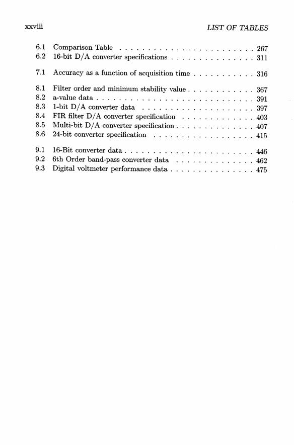
xxviii LIST OF TABLES
6.1 Comparison Table ......... 267 6.2 16-bit D / A converter specifications 311
7.1 Accuracy as a function of acquisition time 316
8.1 Filter order and minimum stability value . 367 8.2 a-value data ............... 391 8.3 I-bit D/A converter data ....... 397 8.4 FIR filter D / A converter specification 403 8.5 Multi-bit D / A converter specification. 407 8.6 24-bit converter specification 415
9.1 16-Bit converter data ..... 446 9.2 6th Order band-pass converter data 462 9.3 Digital voltmeter performance data . 475

List of Symbols
Symbol Description Unit
A Amplitude 1
~A Amplitude deviation 1
AID Analog-to-Digital
Afoldback Ratio between amplifier bandwidth and system bandwidth 1
Ab Amplitude of square wave 1
Ac Amplitude of sine wave 1
Ad Attenuation component: index d 1
Ae Amplitude of error signal 1
Af Amplitude of fundamental 1
Aj Amplitude level: index j 1
Al Limiter constant 1
Arms Root Mean Square amplitude value 1
As Amplitude of sine wave 1
Astopband Stopband attenuation dB ATE Automatic Test Equipment
App Peak-to-peak amplitude 1
An Operational Amplifier: index n 1
Ao Output value of I-bit quantizer 1
Aopenloop Open-loop amplification 1
B Full-Scale Value 1
Bin Input number of bits 1
Bo Most Significant Bit Value 1
Bm mth Bit Value 1
Bn- 1 Least Significant Bit Value 1
Bout Output number of bits 1
xxix

xxx LIST OF SYMBOLS
BER Bit Error Rate 1
C Constant 1
Cbc Base-Collector capacitance F
Cbe Base-Emitter capacitance F Cbex Extra Base-Emitter capacitance F
Cd Diode capacitance F Cg Comparator gain index: g F
CH(old) Hold capacitor F
Cin Input capacitance F CML Current Mode Logic
Cn Capacitor: index n F CMOS Complementary Metal Oxide Semiconductor
Cm Digital code: index m F Cn Capacitor: index n F
D/A Digital-to-Analog
DC Direct Current A
Dn Diode: index n DNL Differential N on-Linearity 1
Dout Digital output data 1 E(.) Statistical expectation 1 ECL Emitter Coupled Logic
ENOB Effective Number of Bits 1 EPS Errors Per Second 1 ERB Effective Resolution Bandwidth Hz
EXOR Exclusive OR function
Eglitch Glitch error Vs
ELSB LSB energy Vs
Enoise Quantization noise voltage V
Etotal Total noise voltage V
Eqns Quantization noise voltage V
E~n8(J) Quantization noise density V2/Hz
f Frequency Hz
fb -3 dB bandwidth Hz
fc Clock frequency Hz
fcomp Comparator -3 dB bandwidth Hz
fin Input signal frequency Hz

LIST OF SYMBOLS XXXI
fose
fqns
fs
fsig
fUGB
FSR GA G{z)
9m H{z) H{w) HS3
!I ft I
AI
Ie Ieomp
Ileakage
lout
IRe!
IEEE INL
io 10 12S h lin
J-FET J{z) k
K{z) LSB m
Oscillation frequency
Quantization noise bandwidth
Sample frequency
Signal bandwidth
Unity Gain Bandwidth
Full-Scale Range
Amplifier gain
Transfer function
Mutual transconductance
Transfer function
System transfer function
High-speed bipolar oxide isolated process
Unity gain bandwidth
Transition frequency
Current
Current deviation
As index
Integrated Circuit
Compensation current
Leakage current
Output current
Reference current
Institute of Electrical and Electronic Engineers
Integral Non-Linearity
Base-Emitter reverse current
Bias current index: 0
Inter IC Signal Standard
Temperature-dependent current
Input current
J unction Field Effect Transistor
Transfer function
Hz
Hz
Hz
Hz
Hz
1
1
1
A/V 1
1
Hz
Hz
A A 1
A A A A
1 A A
A/degree C
A
Boltzmann's constant
Transfer function
Least Significant Bit
As index
1.38 X 10⁻²³ J /K As index
1
1
1
Mean value 1 1
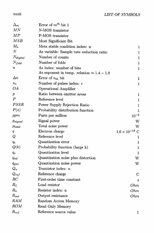
xxxii LIST OF SYMBOLS
Am Error of mth bit 1
MN N-MOS transistor
MP P-MOS transistor
MSB Most Significant Bit
Mn Meta stable condition index: n 1 N As variable: Sample rate reduction ratio 1
Ndigital Number of counts 1
Nlold Number of folds 1 n As index: number of bits 1
As exponent in temp. relation ~ 1.4 - 1.8
An Error of nth bit 1
nr Number of pulses index: r 1 OA Operational Amplifier
P Ratio between emitter areas 1 P Reference level 1
PSSR Power Supply Rejection Ratio 1 P(x) Probability distribution function 1 ppm Parts per million 10-6
Psignal Signal power W Ptotal Total noise power W q Electron charge 1.6 x 10⁻¹⁹ C
Q Reference level 1
qe Quantization error 1 Q(k) Probability function (large k) 1
qs Quantization level 1
qnd Quantization noise plus distortion W
qqns Quantization noise power W Qn Transistor index: n
Qrel Reference charge C
RC First-order time constant s
RL Load resistor Ohm
Rn Resistor index: n Ohm
Rout Output resistance Ohm
RAM Random Access Memory
ROM Read Only Memory
Rrel Reference source value 1

LIST OF SYMBOLS xxxiii
SINAD Signal-to-noise and distortion ratio dB SFDR Spurious Free Dynamic Range 1
SIN Signal-to-noise ratio dB
SIN(J) Signal-to-noise density ratio dB .jHz
SINsystem Signal-to-noise ratio of a system dB
S I Nquantizer Signal-to-noise ratio of quantizer dB
Sn Switch index: n
S Step size 1
Stear Correction factor 1
Stout Output step size 1
SWn Switch index: n
b.Stout Output step size deviation 1
T Absolute temperature K b.T Absolute temperature variation K THD Total Harmonic Distortion
Tconversion Conversion time s
To Reference temperature K Tp Time period index: p s
Tn Transistor index: n
TTL Transistor Transistor Logic
t Time s b.t Time deviation s tmax Maximum time deviation s
td Delay time s
Ottd Delay time difference s
tdif Time difference s
th Hold time s U(t) Unity step function 1
V Potential V b.V Potential deviation V
Va Analog voltage V
VB Battery voltage V
Vbe AC Base-emitter voltage V
VBE DC Base-emitter voltage V VD Diode voltage V
Vdif ference Difference voltage V

xxxiv LIST OF SYMBOLS
Vdroop Droop voltage V
V!s Full-scale voltage value V
Vg Bandgap voltage of silicon 1.208 V
\tid Idle noise voltage V
\tin Input voltage V
Vir Linear voltage range V Vmax Maximum voltage V
Vn Voltage at node index: n V Vout Output voltage V
Vp Peak voltage V
Vre! Accurate reference voltage V
Vrn Reference voltage at node index: n V
vtap Reference tap voltage V
vth Threshold voltage V z Complex frequency for discrete signals
(3 Transistor current gain 1
(3square Unit area MOS gain factor /-lA/V2/-l E Amplitude deviation 1 Em Error index: m 1 ~ Matching deviation 1
7r Angular constant 3.14159
An Integration constant index: n 1 A Global transfer 1
Ab Global transfer of square wave 1
Al Global transfer of limiter 1
Am Maximum value of A 1
As Global transfer of sine wave 1
A Real value 1 (j(P) Standard deviation of P 1
Td Delay time s
en Complex phase rad
w Angular frequency rad/s q> Phase angle rad
Preface
In this introduction an overview of the contents of this book will be given. Analog-to-digital (A/D) and digital-to-analog (D/A) converters provide the link between the analog world of transducers and the digital world of signal processing, computing, and other digital data collection or data processing systems. Numerous types of converters have been designed that use the best technology available at the time a design is made. High-performance submicron CMOS technologies result in high-resolution or high-speed A/D and D / A converters that can be applied in digital audio, digital video, instrumentation and signal processing systems. Furthermore, sub-micron CMOS technologies show an increase in conversion speed into the Giga Hertz range. Applications in these areas are, for example, in high-definition digital television, digital receiver applications, Local Area Networks, cable modem chips and digital oscilloscopes. The availability of high-speed memory chips results in so-called "one-shot" memory applications in these oscilloscopes. In this book different techniques to improve the accuracy in high-resolution A/D and D / A converters will be discussed. Also, special techniques to reduce the number of elements in high-speed A/D converters by a repetitive use of comparators will be described.
In chapter one the application of converters in systems will be discussed. If analog-to-digital and digital-to-analog converters are applied in discretetime systems it is important to perform these operations on frequency-bandlimited signals. In most cases filters are needed to limit the input and output spectrum of the analog signals. If no band limitation is performed, then aliasing of the analog signals into the signal band of interest can occur. General criteria that determine the overall system performance in the case of ideal converters are introduced and defined. Combinations of analog and digital filtering operations result in linear phase filtering over the band of interest. Such a linear phase filtering is very important in digital audio systems.
xxxv

xxxvi Preface
Performance definitions of converters are defined in chapter two. The performance definitions must be unique for a specific parameter. Good parameter definitions of converters are very important in determining the final performance of a discrete-time system. Furthermore, these definitions can be used to compare the performance of different brands of converters. In particular, a good definition of the dynamic parameters of converters is needed. The application of converters in digital audio, digital video systems and digitization of carrier signals, for example, requires these dynamic specifications. Many converters that originally were designed for high-accuracy measurement system applications are not optimized for dynamic operations. In digital audio, for example, many specifications, that are important in instrumentation (such as offset, full-scale accuracy, temperature drift) are of minor value. The specific dynamic parameters must therefore be defined and related to important design parameters. Glitches in D / A converters introduce distortion in digital audio systems, while in video display systems fuzzy images are obtained. Definitions like Effective Number of Bits (ENOB), Spurious Free Dynamic Range (SFDR), jitter of the sampling clock and interconnect wire delay will be correlated to Integral Non-Linearity (INL) and Differential Non-Linearity (DNL) specifications. Furthermore quantization spectra and the influence on the linearity specification will be derived.
In general it can be said that the number of systems and circuits that can perform analog-to-digital conversion is much larger than the number of structures and basic solutions to digital-to-analog conversion. In chapter three examples of high-speed analog-to-digital converters are discussed. Up until now the full-flash converter was considered the fastest converter type that can be designed. This, however, is only partly true. Due to the use of a large amount of components for example, in an 8-bit converter 255 comparators are needed to detect every code level the size of such a converter becomes large with respect to the time a signal needs to travel over the interconnection lines on a chip. In high-speed converters the time difference for signals traveling at the top of the converter structure with respect to signals traveling in the middle of the structure may become in the order of pico seconds. At high-input frequencies these time differences in signal transfer introduce distortion. Depending on input frequency and resolution of a converter, timing differences may not exceed pico second values. When taking into account that the transmission speed over the interconnection lines in sub-micron CMOS integrated circuit is about one-third of the speed of light, then 1 psec equals about 100 microns of interconnect. When the
Preface xxxvii
size of an analog-to-digital converter chip without sample-and-hold amplifier increases, it is practically impossible to match clock- and signal-line delays within the required timing accuracy. Therefore, improved converter systems with a reduced chip size using a continuous input-signal folding architecture overcome these problems. In a final system implementation of such a system, only zero crossings of the analog signal are important for the converter accuracy. To reduce the number of input amplifier-comparator stages in such a system, an interpolation of zero crossings is used. This system results in a compact very high-performance analog-to-digital converter structure. In an MOS technology switches and capacitors are the main design elements. The input signal can be stored on multiple capacitors and then a comparison is made to perform an AjD conversion. Subranging or two-step system solutions can be easily implemented. These systems show a very good performance close to the ideal converter at reasonable high sampling rates. Finally pipeline converters will be discussed. These systems can use a 1.5 bit per stage or multi-bit per stage conversion units. The multi-bit per stage can suffer from linearity problems in the first stages depending on the resolution of the converter. Calibration of these stages can overcome these problems.
High-speed digital-to-analog converters discussed in chapter four show good performance at sampling frequencies up to 1 GSamplejs. These converters can use binary weighted capacitor arrays. In modern technologies capacitor matching is good enough to obtain a full linearity specification up to 12-bit resolution without trimming. However, most high-speed digital-toanalog converters use segmented current source structures in combination with binary weighting of current sources. The segmentation improves linearity and guarantees monotonicity, while furthermore it is more easy to obtain a low glitch energy under dynamic operation of the converter. Especially the performance at high output signal frequencies is discussed in a couple of designs. Timing is the most important issue after obtaining the linearity specification. In high-accuracy analog-to-digital and digital-to-analog converters the accuracy with which the binary weighting of the bit weights is performed is an important design criterion. In chapters five and six generally applicable methods to obtain high-accuracy converters will be introduced. These methods will mainly use a combination of accuracy introduced by matched elements and a dynamic method to improve the limited passive accuracy. Resistor or capacitor matching in integrated circuits limits the resolution of converters based on these elements to about twelve bits. Trimming methods

xxxviii Preface
can be used to overcome this problem. These trimming methods, however, are expensive, while in addition changes of the trimmed elements due to time or temperature variations destroy the accurate trimming of the converter. In MOS technologies accuracy is obtained by matching binary weighted capacitor banks. Accuracies of ten to twelve bits are possible without trimming.
When monotonicity of a converter is the most important design criterion then special system configurations are possible. Solutions based on current swapping or voltage division will be described. These systems are inherently monotonic while overall linearity is limited.
When the absolute accuracy in a converter is required, then special systems are needed. Systems which convert the digital value into an accurate time need a limited amount of accurate elements. However, speed is limited, while systems with higher sampling rates suffer from extremely high clock frequencies which result in high-frequency signal radiation.
To overcome these problems a combination of passive and active matching of components will be used. The first method combines accurate passive division with a time interchanging concept to obtain a very high weighting accuracy without using accurate elements. Furthermore, this method is independent of element aging and remains accurate over a large temperature range. Examples of digital-to-analog and analog-to-digital converters will be given that use this special method. In an MOS technology calibration of current sources can be used to obtain a segmented converter structure. Such a structure is less sensitive to element matching, while the calibration of the individual current sources makes the system independent of element aging and less temperature-sensitive. The gate capacitance of an MOS device is used to store the error signal information that is needed to calibrate the bit current sources.
In high-speed, high-accuracy analog-to-digital converters the analog input signal must be sampled and kept constant during the time the conversion takes place. High-resolution, high-speed and high-accuracy sample-and-hold amplifiers are a key element for analog-to-digital conversion in, for example, digital video, digital audio or carrier signal conversion. In chapter seven sample-and-hold amplifiers are discussed. A high-performance sample-andhold amplifier in front of a parallel-type AID converter can for example improve at high frequencies the dynamic performance of such a converter. The sampling of the analog signal in this way is performed by the sample-

Preface xxxix
and-hold amplifier. Distortion introduced by timing uncertainties at high frequencies in the flash converter can be avoided in this way. Only a single switch in the sample-and-hold amplifier determines the timing accuracy.
Different examples of sample-and-hold amplifiers are shown. Furthermore in sub-micron technology the sampling switches may become a problem. Therefore clock bootstrapping techniques will be shown that improve the performance of the sampling switches. In chapters eight and nine examples of noise-shaping techniques to improve the dynamic range of a system are described. Such techniques are very useful when speed can be exchanged with accuracy or with the word length used in a system.
An ultimate of the noise-shaping techniques are the well-known sigma-delta AID and D I A converters which basically use a noise-shaping filter in cooperation with a quantizer and a I-bit DI A or AID converter stage. Such a I-bit converter is extremely linear, which results in a very good differential linearity of such a converter. The most important design criteria and limitations will be given. At the moment the dynamic range of a system must be increased but the maximum clock speed in the system cannot be enlarged, then a multi-bit D I A converter can be used in the feedback loop. At that moment, however, the linearity of the D I A converter determines the overall linearity of the converter. Therefore, dynamic element matching in the form of Data Weighted Averaging or other error randomizing techniques can be used. The root locus method can be used successfully to determine the stability of noise-shaping coders. However, modeling a quantizer simply with a variable gain is not sufficient to predict the stability at small signals of the converter. Therefore a modified model using a variable gain and a phase uncertainty is introduced. This model predicts the small signal stability of the converters pretty well. Especially when a higher-order noise-shaping filter is used, the stability analysis gives an insight in the operation of the system when small input signals are applied. A noise-shaping coder is said to be stable when an idle pattern at half the sampling frequency is present under nearly all input signal conditions. Different architectures will be described which introduce a high-order noise-shaping filter architecture without running into a stability problem. A special system that uses a signal-level-dependent filtering order implements a kind of feed-forward coupling in the filtering function. At low-level input signals a high-order filtering function is present, but at the moment the signal in the loop increases in amplitude, the filter order is

xl Preface
reduced. In this way a very good optimum between filter order and stability of operation is obtained. Examples of designed 16- to 20-bit D / A converters using 1-bit or multi-bit D/ A converters will be described. The MASH structure that uses a cascade of first or second order noiseshaping stages prevents the problem of instability while at the same time a higher order noise-shaping filtering operation is performed. Bandpass sigma-delta modulators are added to complete the overview. A specific design using a continuous time noise-shaping filter shows already very good performance for applications in digital radio systems. Finally an example of a 5-digit digital voltmeter system that completes chapter eight will be given.
Low-noise high-stability reference sources are a basic element in converters. Different methods to obtain accurate and temperature insensitive reference sources will be given in chapter ten. The temperature dependence of the bandgap voltage (about 1.2 V) reference sources is small and in CMOS the parasitic substrate bipolar PNP devices are used for this purpose. The noise analysis of these systems is performed. In signal processing applications the absolute value of the reference source is not always important. System noise might be dominant and therefore reference sources must be designed for minimum noise performance. In low-voltage systems (1 V) the bandgap designs are difficult and mostly higher voltages are used to solve this problem.
In high-speed analog-to-digital converters that are based on the full-flash or folding principles, the question about the relation between maximum analog input frequency and the bandwidth of the comparator-amplifier stages arises. In chapter eleven an analysis that determines the relation between the maximum analog input frequency and the bandwidth of the comparatoramplifier stages is performed. Furthermore it will be shown from this analysis that a limited analog bandwidth of the system results in third-order signal distortion. This distortion can fold signals back into the baseband of the converter and results in a reduction of the signal-to-noise ratio of the system. The maximum analog input frequency will be defined as that input frequency for which the signal-to-noise ratio is reduced by a value equal to half the least significant bit. The number of effective bits as a function of input frequency will be used as an accurate measure for the performance of high-speed analog-to-digital converters. A second analysis about the decision failure of comparators in flash-type converters is performed. This analysis gives insight in the relation between the bit error rate (BER) of a comparator as a function of the gain-bandwidth product of a technology.
Preface xli
Comparator stages can be optimized for a minimum error.
In chapter twelve attention is paid to sub-micron CMOS technologies. Especially matching of components is a very important requirement. Most systems used today have a differential signal operation to reduce cross talk from other (mostly digital) system parts. Results and design issues are given in this chapter. Components in an integrated circuit are best matched when they are placed close to each other. Furthermore, these devices must be placed on chip using an isothermal boundary. When more devices such as transistors or resistors must have a very good matching, care must be taken that neighboring, not active elements are placed at the edges of the layout of such a system. In this wayan improvement in matching between the individual elements of the array is obtained. After defining the important specifications of converters, good measurement set-ups and definitions are needed. In chapter thirteen attention is paid to measuring the static and dynamic performance of converters. Usually DC parameters can be measured with automatic test equipment and are well defined. Much attention has been paid to obtaining measurements and measurement set-ups which give the required parameter in a fairly simple way and use a well-defined test condition. One of the most important parameters to be determined in this way is the dynamic performance of a system. The dynamic range is determined by measuring the signal-to-noise ratio of a converter over half the sampling frequency. This signal-to-noise ratio must, in the case of a well-designed converter, be close to the theoretical value, which is defined over a bandwidth equal to half the sampling frequency. When large discrepancies are found, then this converter is not designed to operate under dynamic conditions. Sometimes it is possible to overcome some of the problems by adding external circuitry, which, for example, can be a deglitcher circuit to reduce the glitch of the converter or by adding data latches which perform the switching of the bit weights in a digital-to-analog converter at the same time moment.
During the writing of this book an attempt has been made to discuss the most important parameters and design criteria and giving worked-out examples of practical circuits and systems. On the other hand, no attempt has been made to be complete and cover all subjects in detail. By including practically worked-out examples, what in a number of cases are products supplied by semiconductor manufacturers, the reader gets familiar with design problems and practical system implementations under real conditions.

xlii Preface
For the most part, these implementations differ quite a lot from the basic system solution. Furthermore this book is not written to be complete. Always it can be improved and system or circuit solutions that are more optimal to perform a function will be available or will soon be. An attempt has been made to include important design examples from literature to give the reader an insight on what can be obtained in CMOS technology. Furthermore circuits or systems are mostly briefly discussed. The size of the book would increase too much in case all circuits should have been discussed more detailed. Therefore the limited description has been used. The reader can copy the publication from IEEE in case he is interested in more detailed analysis and study the specific system.