cms conference reportcdsweb.cern.ch/record/687411/files/cr02_004.pdf · cms conference report ......
TRANSCRIPT
Available on CMS information server CMS CR 2002/004
CMS Conference Report
25 March 2002
Developments in Particle Detection
Tejinder S. Virdee
Imperial College, London, UK.
Abstract
From the many recent developments in particle detectors we select some of the major and challengingones. The selected developments are primarily those necessitated by the harsh environment of theLHC. The presentations made in the parallel sessions of this conference are mostly placed in the con-text of these developments. This includes those connected with two new experiments concepts whichwere presented namely: TESLA and BTeV. From the inner tracking we look at pixel detectors, siliconmicrostrip detectors and microstrip gas detectors; from calorimetry we consider PbWO4 scintillatingcrystals and the ’accordion’ liquid argon calorimeter; from the muon systems we consider monitoreddrift tubes (MDTs), thin-gap chambers (TGCs) and resistive plate chambers (RPCs). Another subjectcovered, and much reported in the parallel sessions, is that of photodetectors including avalanche pho-todiodes (APDs), vacuum phototriodes (VPTs), hybrid photodiodes (HPDs) and visible light photondetectors (VLPCs). Finally the important subject of electronics is discussed.
Presented at EPS Conference. July 12-18, 2001, Budapest
1 IntroductionA major R&D effort in particle detectors was required during the last decade to select detectors that could surviveand operate reliably in the harsh environment of the Large Hadron Collider (LHC). For each sub-detector tech-nology retained, several others were also investigated. Development of new particle detectors takes a long timeand goes through many phases starting from the idea or concept, progressing through intensive R&D, prototyping,systems integration, installation and commissioning and finally data taking. This can be illustrated using any oneof the many detector technologies in the LHC experiments.
We have chosen lead tungstate scintillating crystals, used for the electromagnetic calorimeter of CMS, as an illus-trative example [1, 2].
- Idea: in 1992 some yellowish samples of a few cc were shown - the final volume required is 10 m3 !!
- R&D: 1993-2000: much work was carried out to increase the size of crystals (both length and cross-section),requiring improvements in the growing technique for heavier and heavier crystals. Improvements in theradiation hardness required optimization of stoechiometry (fraction of lead oxide and tungsten oxide), of thepurity of raw materials (balance cost v/s level of purity), and compensation of defects by specific doping(production crystals are now doped with Yttrium and Niobium).
- Prototyping: 1994-2000: performance of larger and larger matrices of crystals was studied in test beams- this should culminate in a test in 2002 of a prototype ’basket’ comprising 400 crystals. The informationgleaned from the earlier prototypes was fed back into the R&D e.g. in 1997 significant radiation inducedattenuation (through creation of colour centers) was observed at a low dose rate (∼ 1 Gy/hr) leading toa drop in the collected light. The extent of the loss depended on the dose rate and exhibited saturation.However after irradiation recovery of the light signal was observed. Through R&D the light loss has beenreduced by a factor of 5 at saturation: now it is ∼ 3-5 %.
- Mass manufacture: 2000-2006: a sizeable and high-yield crystal growing capability had to be put in place -around 130 ovens had to be refurbished and computer-control implemented. The diameter of the boules hasbeen steadily increased so that now two crystals, and probably 4 crystals, can be obtained from one boule.
- Systems integration: 2001-2003: the crystals are assembled into the specially developed light and thinmechanical structures, the electronics, cooling system and signal and voltage cables have to be integratedinto each one of 36 phi ’super-modules’ comprising 4 ’baskets’ each.
- Test beam calibration (2002-2006)
- Data taking is foreseen in 2006.
It can be seen that almost one and half-decades will have passed from the concept to physics data taking!
2 New ExperimentsTwo new experiment designs were presented in the parallel session namely TESLA [3] and BTeV [4]. It is clearthat this new generation of experiments can benefit from the development of detectors for LHC and can thereforeenter into the detector development cycles at later stages. The time from conception to completion can hence beshortened. We shall briefly describe these detectors in order to pull out novel detector technologies and place themin the context of the development of some of the LHC detectors.
2.1 The TESLA Detector
The parameters of the various electron-positron colliders are compared in Table 1. At TESLA the repetition rate is5 Hz with 2820 bunches/train.
The main requirements for the TESLA detector are similar to those for the pp LHC experiments and are summa-rized below:
- Good momentum resolution of δ(1/pT ) < 5.10−5 GeV−1 that is driven by the need for a precise measure-ment of recoil mass in processes such as e+e− → Z (→ ``)H . The desired resolution is similar to that inATLAS and CMS but a factor 10 better than that in LEP detectors.
2

Table 1: Some of the parameters of TESLA compared with those of LEP and SLC
TESLA LEP SLCEnergy (GeV) 500 209 92
Luminosity (cm−2s−1) 3.4×1034 6×1031 3×1030
Bunch Spacing (ns) 337 22000 8.3×10⁶
Beam size (x, y) (nm) 553, 5 3×10⁵, 8000 1500, 650
- Vertexing - an impact parameter resolution of δ(impact parameter) < 5µm + 10µm / (psin3/2θ). Such aresolution is necessary for identifying final states containing c, b and t quarks in order to determine thebranching ratios of H → bb, cc, tt. High purity and high efficiency tagging of c and t as well as b isrequired.
- Energy flow - a large number of jets is expected in final states such as ZH → qq + bb (i.e. 4j incl 2b),tt → bW , bW (i.e. 6j incl 2b), HA → tt + tt (12j incl 4b). Beamstrahlung, initial state radiation and thecomplex topology of such final states makes kinematics fits difficult.
- Hermiticity - missing ET is an important signature for SUSY processes.
The single most important aspect of detector design is the choice of the magnet field configuration. In orderto satisfy the above requirements a detector configuration similar to that of CMS has been chosen (Fig. 1); alarge-bore 3-4 T solenoid enclosing the inner tracking and calorimetry with the muon placed system outside. Thechallenge associated with the design and construction of high field solenoids is considered in Section 3.
Figure 1: The transverse view of the TESLA detector. All dimensions are in mm.
The inner tracking comprises a large volume TPC complemented by a multi-layer semiconductor vertex detector.The TPC provides a large number of measurement points for a minimum of material per point. It will be read-out continuously with data from about 160 bunch crossings overlaid during a drift time of 55 µs. During thisinterval ∼ 0.01 high-energy hadronic event is expected. One readout technology being considered is the gaselectron multiplier (GEM) coupled with microstrip gas chambers (MSGCs) (see Section 4.3). In GEM and MSGCdetectors the problem of ion feedback is naturally reduced and GEM detectors lend themselves to gating that canfurther reduce ion feedback if required.
3
The vertex detector is designed to have a resolution of a factor two better than that achieved by SLD that usedCCD technology: σ(ip)rφ=4.2 µm ⊗ 4.0 µm/(psin3/2θ), where ⊗ signifies the root of the quadratic sum of theterms and p is in GeV/c. This is achieved by 20×20 µm2 pixels with a first layer at a radius of 1.5 cm from thebeam-line. The expected hit rate in TESLA is 0.03 hits/mm2/bunch crossing. Alternative technologies are CMOSmonolithic pixels and hybrid pixels. All three approaches require considerable R&D before use at TESLA. This isconsidered in Section 4.1.
Both the electromagnetic and hadronic calorimeters will be highly segmented to disentangle multi-jet events andenable use of energy flow algorithms. The aim is to improve the jet energy measurement by using the momenta ofcharged tracks measured in the inner tracking, the energies of photons and electrons measured in the ECAL and theenergies of neutral hadrons measured in the hadron calorimeter. For optimal use of the energy-flow technique it isadvisable to place the calorimetry inside the coil. Clearly the precision attained will depend on how the momentaand energies are combined, for which dense highly granular calorimeters are of great value. The electromagneticcalorimeter is planned to have a segmentation of 1×1 cm2 using sampling of 1.4 mm tungsten/Si. The hadroniccalorimeter uses 2 cm Fe/ scintillators with WLS fibre readout. The smallest tile size is 5×5 cm2.
Since the bunch trains are ∼ 1 ms long, data have to be buffered before being read-out during the long inter-traininterval of 200 ms.
2.2 BTeV
BTeV is designed to measure CP violation parameters in the b-quark system at the Tevatron. The special featuresare:
- a precision vertex detector comprising 31 pixel planes using hybrid pixels
- particle identification assured by RICH detectors
- good measurement of mass of final states containing photons using a lead tungstate electromagnetic calorime-ter.
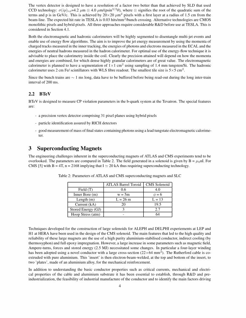
3 Superconducting MagnetsThe engineering challenges inherent in the superconducting magnets of ATLAS and CMS experiments tend to beoverlooked. The parameters are compared in Table 2. The field generated in a solenoid is given by B = µ0nI. ForCMS [5] with B = 4T, n = 2168 implying that I ' 20 kA thus requiring superconducting technology.
Table 2: Parameters of ATLAS and CMS superconducting magnets and SLC
ATLAS Barrel Toroid CMS SolenoidField (T) 0.6 4.0
Inner Bore (m) w = 5m φ = 6Length (m) L = 26 m L = 13
Current (kA) 20 19.5Stored Energy (GJ) 3 2.7Hoop Stress (atm) - 64
Techniques developed for the construction of large solenoids for ALEPH and DELPHI experiements at LEP andH1 at HERA have been used in the design of the CMS solenoid. The main features that led to the high quality andreliability of these large magnets are the use of a high purity aluminium-stabilised conductor, indirect cooling (bythermosyphon) and full epoxy impregnation. However, a large increase in some parameters such as magnetic field,Ampere-turns, forces and stored energy (2.5 MJ) necessitated some changes. In particular a four-layer windinghas been adopted using a novel conductor with a large cross-section (22×64 mm2). The Rutherford cable is co-extruded with pure aluminium. This ’insert’ is then electron-beam-welded, at the top and bottom of the insert, totwo ’plates’, made of an aluminium alloy, for the mechanical reinforcement.
In addition to understanding the basic conductor properties such as critical currents, mechanical and electri-cal properties of the cable and aluminium substrate it has been essential to establish, through R&D and pre-industrialization, the feasibility of industrial manufacture of the conductor and to identify the main factors driving
4
its cost. Final full-lengths of the conductor are now being manufactured and the CMS magnet is scheduled for testin mid-2004.
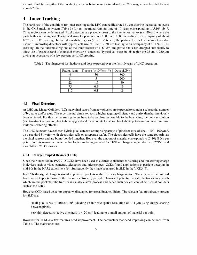
4 Inner TrackingThe harshness of the conditions for inner tracking at the LHC can be illustrated by considering the radiation levelsin the CMS tracking system (Table 3) for an integrated running time of 10 years corresponding to 5.105 pb−1.Three regions can be delineated. Pixel detectors are placed closest to the interaction vertex (r < 20 cm) where theparticle flux is the highest. The typical size of a pixel is about 100 µm × 100 µm leading to an occupancy of about10−4 per LHC crossing. In the intermediate regions (20 < r < 60 cm) the particle flux is low enough to enableuse of Si microstrip detectors with typical cell size of 10 cm × 50 µm leading to an occupancy of ' 1 % / LHCcrossing. In the outermost regions of the inner tracker (r > 60 cm) the particle flux has dropped sufficiently toallow use of gaseous (and of course Si microstrip) detectors. Typical cell sizes in this region are 25 cm × 250 µmgiving an occupancy of a few percent per LHC crossing.
Table 3: The fluence of fast hadrons and dose expected over the first 10 years of LHC operation.
Radius (cm) Fluence (×1014cm−2) Dose (kGy)4 30 80011 5 20022 1.5 8075 0.3 8
115 0.1 2
4.1 Pixel Detectors
At LHC and Linear Colliders (LC) many final states from new physics are expected to contain a substantial numberof b-quarks and/or taus. The experimental aim is to reach a higher tagging efficiency and purity than has previouslybeen achieved. For this the measuring layers have to be as close as possible to the beam-line, the point resolution(and two-track separation) has to be very good and the amount of material has to be kept to a minimum to minimizemultiple scattering effects.
The LHC detectors have chosen hybrid pixel detectors comprising arrays of pixel sensors, of size ∼ 100×100 µm2,on a standard Si wafer, with electronics cells on a separate wafer. The electronics cells have the same footprint asthe pixel sensors and are bump-bonded together. However the amount of material corresponds to (5-10) % X0 perpoint. For this reason two other technologies are being pursued for TESLA: charge coupled devices (CCDs), andmonolithic CMOS sensors.
4.1.1 Charge Coupled Devices (CCDs)
Since their invention in 1970 2-D CCDs have been used as electronic elements for storing and transferring chargein devices such as video cameras, telescopes and microscopes. CCDs found applications as particle detectors inmid-80s in the NA32 experiment [6]. Subsequently they have been used in SLD in the VXD3 [7].
In CCDs the signal charge is stored in potential pockets within a space-charge region. The charge is then movedfrom pocket to pocket towards the readout electrode by periodic changes of potential on gate electrodes underneathwhich are the pockets. The transfer is usually a slow process and hence such devices cannot be used at colliderssuch as the LHC.
However CCD-based detectors appear well adapted for use at linear colliders. The relevant features already presentfor SLD are:
- small pixel sizes of 20×20 µm2, yielding an intrinsic spatial resolution of ∼ 4 µm using charge sharingbetween pixels.
- very thin detectors (active thickness is ∼ 20 µm) leading to a small amount of material per point
However for TESLA a few features need improvement. The parameters that need improving can be seen fromTable 4. The major ones are:
5

- develop architectures to increase the speed of the pixel readout. VXD3 had a readout time of 180 ms! Thebackground, mainly from e+e− pairs, at r = 1.5 cm is estimated to give 0.03 hits/mm2/bx. Because of theTESLA beam structure the resulting ∼ 100 hits/mm2 (4 % occupancy) is not comfortable even at 50 MHzreadout speed.
- improvement of radiation hardness to a 1 MeV-equivalent neutron fluence of 1010 n/cm2.
- develop thin mechanical structures to mount the CCDs
Table 4: The performance improvement factors required for LC CCD vertex detector
SLD LC FactorLongest CCD (mm) 80 125 1.6
Largest CCD area (mm2) 1280 3000 2.3Ladder Thickness ( % X0) 0.4 0.12 3.3
Layer 1 radius (mm) 28 12 2.3Readout rate (MHz) 5 50 10
N pixels (M) 307 700 2.3
The active thickness of pixels is 20 µm. In order to keep the material at a minimum a method needs to be developedto thin down the pixels wafer and then to mount them on thin Be substrates.
Radiation damage could be an issue though the expected n-fluence is several orders of magnitude lower than thatexpected at the LHC. In a sensitive thickness of 20 µm the signal from a mip is only ∼ 2000 e. This chargehas to undergo hundreds of serial transfers before readout. In damaged detectors charge can be trapped in crystaldefects. As crystal defects are especially abundant in the surface region, it is desirable to move the region of signalgeneration a certain distance away from the Si-SiO2 interface into the bulk. At the same time the speed of chargetransfer also increases. This movement at a small distance from the surface is done in what is named a ’buried-channel’ CCD. The charge is moved to an output electrode the size of which can be made very small, so that thedetector capacity as seen by the readout electronics is very low (10-100 fF). However it is necessary to integrate atleast part of the electronics onto the detector so that stray capacitances in leads (∼ pF) can be avoided.
4.1.2 Monolithic CMOS Pixel Sensors
These are novel position sensitive devices that integrate a 2-D array of detecting diodes and the associated readoutelectronics on the same Si substrate [8]. Hence the bump-bonding step, necessary for hybrid pixels, can be avoided.
The architecture is similar to that of the visible light CMOS camera that is emerging as a competitor to the standardCCDs for digital photography. A thin epitaxial layer of low-resistivity silicon is used as the sensitive detectorvolume. The charge generated by the traversing charged particle (∼ 80 electron-hole pairs per micron) is collectedby an n-well/p-epi diode, created by n-well implantation into the epitaxial layer. The electrons liberated in thislayer diffuse towards the diode within a typical time of a few tens of nanoseconds. Because of the three ordersof magnitude between the doping levels of the p-epitaxial layer and of the neighbouring p++ wells and substrate,potential barriers are created at the region boundaries, that act like mirrors for the excess electrons (Fig. 2).
This principle was tested using 120 GeV/c pion beams on two prototype chips, each with 64×64 square pixelswith almost a 100 % fill-factor (active area), labeled MIMOSA I or II. The relevant characteristics and results aregiven in Table 5 [8].
As can be seen an excellent spatial resolution can be achieved with these very thin structures. However a 50 %decrease in the collected charge was observed after proton irradiation with a fluence of ∼ 5×10¹¹ p/cm2. FurtherR&D is needed to design faster read-out, demonstrate feasibility on full-scale chips (∼ 2×2 cm2) and to improveradiation hardness. An important advantage of this approach is that standard sub-micron CMOS commercialfabrication processes can be used, which should lead to reduced cost and inherent radiation hardness, though thelatter has still to be demonstrated. This is still an immature technique and may have a high potential.
4.1.3 Hybrid Pixels.
The LHC experiments employ hybrid pixel detectors close to the interaction region. The electronic cell containsamplification/shaping elements and circuitry to allow hit data to be stored on the edge of the chip awaiting readout
6

p+ p+ N+NWELLPWELL PWELL
---
-
----
--
-
-
--
-
---
-
++
++++
+
+++
++
+
++++
++
m.i.p.
PASSIVATIONOXIDE
DEPLETIONZONEEPI-LAYERP
SUBSTRATEP++ JV_3
16
Figure 2: Charge collection within a CMOS pixel, indicating the potential barriers.
Table 5: Characteristics and results from two CMOS monolithic pixel detectors.
MIMOSA I MIMOSA IIFabrication Process 0.6 µm 0.35 µm
Epitaxial Layer Thickness 14 µm 5 µmCharge Collection Time 150 ns 100 ns
Readout Clock Frequency 5 MHz 25 MHzCollected Charge (seed pixel) 300 e 110 eCollected Charge (3×3 pixels) 900 e 315 e
Efficiency 99.5 % 98.5 %Spatial Resolution, σx 1.4 µm 2.2 µm
upon receipt of a trigger.
An example of a hybrid pixel detector is the CMS pixels detector [9]. CMS has chosen n+ pixels on n-type Sisubstrate. The size of the pixels is 150µm × 150µm. The choice of substrate material is motivated by the largeLorentz angle (340) for electrons in the 4T field that leads to a sizeable charge sharing among the pixels. Thespatial resolution in rφ is ∼ 15 µm.
Results were presented from tests of BTeV prototype sensors bonded to 0.25 µm ’deep-submicron’ electronics (seeSection 8) [4]. The size of the pixels was 50 × 400 µm2. A rφ spatial resolution of ∼ 9 µm was measured and theamplifier response was found not to change after irradiation up to a dose of 33 Mrad.
It appears unlikely that such a technique will be employed at the LC due to the large material thickness and largepixel sizes. However they afford a fast readout and exhibit high radiation resistance. Such a technique could wellbe suitable for upgrades of the closest-to-beam Si microstrip detectors at the LHC.
4.2 Silicon Microstrip Detectors
Silicon microstrip detectors are perhaps ideal detectors for inner tracking in the pp experiments at the LHC. Theyare fast (charge can be collected within an inter-bunch crossing time of 25 ns), can give very good spatial resolution
7
(∼ 20-50 µm leading to good momentum resolution) and a good two-track resolution (tracks inside high pT jetscan be separated). However in the early 1990’s at the conceptual design stage of the LHC experiments, it wasfar from evident that large areas of Si microstrip detectors could be deployed. Radiation damage of detectorswas poorly understood (hadron fluences of 1014 /cm2 have to be withstood at the LHC), the costs of fabricationappeared prohibitive (100s of m2 are required) and the per channel electronics cost had to be brought down to ∼ afew CHF/channel (tens of millions of channels are required).
In the early 1990’s results [10, 11, 12] from irradiation up to the levels anticipated at the LHC showed a sizeableleakage current, that rises linearly with fluence, but more seriously that the effective doping of the bulk changedleading to type-inversion (n-type material becomes p-type). Progressively higher and higher bias voltage is thenrequired (∼ several hundred volts) for full depletion. However, the available detectors could only be biased up to ∼100 V before exhibiting breakdown. It was also observed that the doping changes continued after the terminationof irradiation for detectors kept at room temperature (’reverse annealing’).
Considerable R&D has been carried out to improve the understanding of the damage mechanisms, working outstrategies to prolong the useful lifetime of irradiated detectors and to improve the HV behaviour of the detectors.
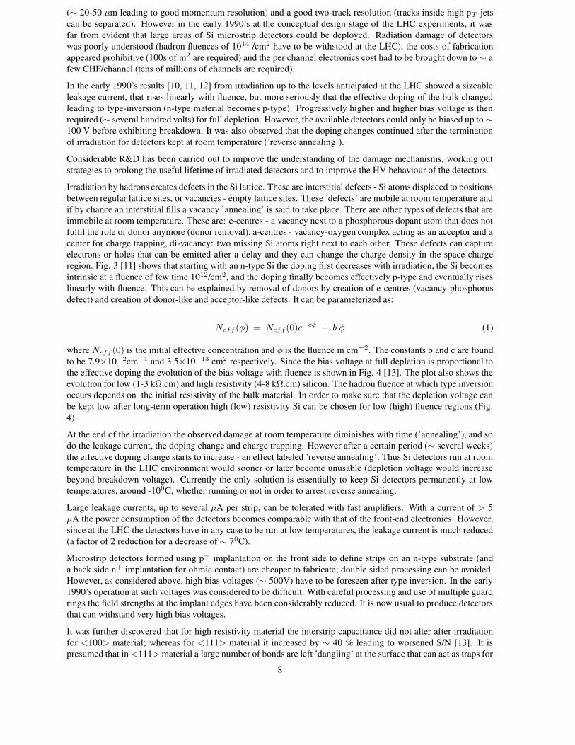
Irradiation by hadrons creates defects in the Si lattice. These are interstitial defects - Si atoms displaced to positionsbetween regular lattice sites, or vacancies - empty lattice sites. These ’defects’ are mobile at room temperature andif by chance an interstitial fills a vacancy ’annealing’ is said to take place. There are other types of defects that areimmobile at room temperature. These are: e-centres - a vacancy next to a phosphorous dopant atom that does notfulfil the role of donor anymore (donor removal), a-centres - vacancy-oxygen complex acting as an acceptor and acenter for charge trapping, di-vacancy: two missing Si atoms right next to each other. These defects can captureelectrons or holes that can be emitted after a delay and they can change the charge density in the space-chargeregion. Fig. 3 [11] shows that starting with an n-type Si the doping first decreases with irradiation, the Si becomesintrinsic at a fluence of few time 1012/cm2, and the doping finally becomes effectively p-type and eventually riseslinearly with fluence. This can be explained by removal of donors by creation of e-centres (vacancy-phosphorusdefect) and creation of donor-like and acceptor-like defects. It can be parameterized as:
Neff (φ) = Neff (0)e−cφ − b φ (1)
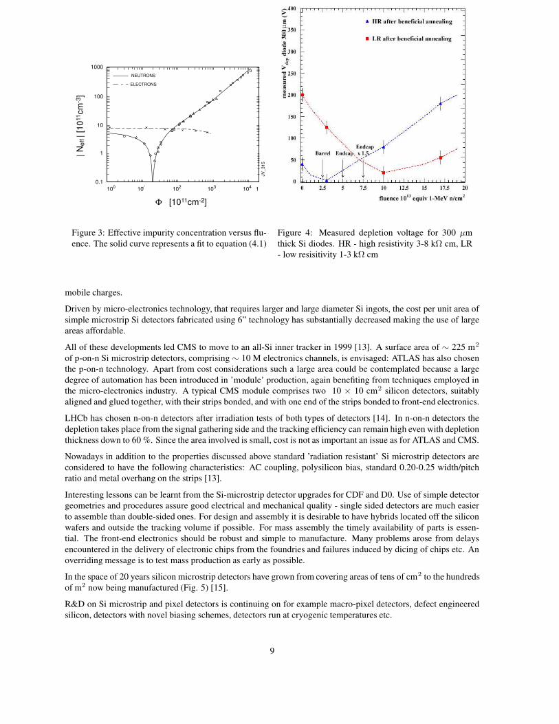
where Neff (0) is the initial effective concentration and φ is the fluence in cm−2. The constants b and c are foundto be 7.9×10⁻²cm−1 and 3.5×10⁻¹³ cm2 respectively. Since the bias voltage at full depletion is proportional tothe effective doping the evolution of the bias voltage with fluence is shown in Fig. 4 [13]. The plot also shows theevolution for low (1-3 kΩ.cm) and high resistivity (4-8 kΩ.cm) silicon. The hadron fluence at which type inversionoccurs depends on the initial resistivity of the bulk material. In order to make sure that the depletion voltage canbe kept low after long-term operation high (low) resistivity Si can be chosen for low (high) fluence regions (Fig.4).
At the end of the irradiation the observed damage at room temperature diminishes with time (’annealing’), and sodo the leakage current, the doping change and charge trapping. However after a certain period (∼ several weeks)the effective doping change starts to increase - an effect labeled ’reverse annealing’. Thus Si detectors run at roomtemperature in the LHC environment would sooner or later become unusable (depletion voltage would increasebeyond breakdown voltage). Currently the only solution is essentially to keep Si detectors permanently at lowtemperatures, around -100C, whether running or not in order to arrest reverse annealing.
Large leakage currents, up to several µA per strip, can be tolerated with fast amplifiers. With a current of > 5µA the power consumption of the detectors becomes comparable with that of the front-end electronics. However,since at the LHC the detectors have in any case to be run at low temperatures, the leakage current is much reduced(a factor of 2 reduction for a decrease of ∼ 70C).
Microstrip detectors formed using p+ implantation on the front side to define strips on an n-type substrate (anda back side n+ implantation for ohmic contact) are cheaper to fabricate; double sided processing can be avoided.However, as considered above, high bias voltages (∼ 500V) have to be foreseen after type inversion. In the early1990’s operation at such voltages was considered to be difficult. With careful processing and use of multiple guardrings the field strengths at the implant edges have been considerably reduced. It is now usual to produce detectorsthat can withstand very high bias voltages.
It was further discovered that for high resistivity material the interstrip capacitance did not alter after irradiationfor <100> material; whereas for <111> material it increased by ∼ 40 % leading to worsened S/N [13]. It ispresumed that in <111> material a large number of bonds are left ’dangling’ at the surface that can act as traps for
8
NEUTRONS
ELECTRONS
1000.1
1
10
100
1000
10⁄ 102 103 104 1
Φ [1011cm-2]
| Nef
f | [1
011 c
m-3
]
JV_3
15
Figure 3: Effective impurity concentration versus flu-ence. The solid curve represents a fit to equation (4.1)
Figure 4: Measured depletion voltage for 300 µmthick Si diodes. HR - high resistivity 3-8 kΩ cm, LR- low resisitivity 1-3 kΩ cm
mobile charges.
Driven by micro-electronics technology, that requires larger and large diameter Si ingots, the cost per unit area ofsimple microstrip Si detectors fabricated using 6” technology has substantially decreased making the use of largeareas affordable.
All of these developments led CMS to move to an all-Si inner tracker in 1999 [13]. A surface area of ∼ 225 m2
of p-on-n Si microstrip detectors, comprising ∼ 10 M electronics channels, is envisaged: ATLAS has also chosenthe p-on-n technology. Apart from cost considerations such a large area could be contemplated because a largedegree of automation has been introduced in ’module’ production, again benefiting from techniques employed inthe micro-electronics industry. A typical CMS module comprises two 10 × 10 cm2 silicon detectors, suitablyaligned and glued together, with their strips bonded, and with one end of the strips bonded to front-end electronics.
LHCb has chosen n-on-n detectors after irradiation tests of both types of detectors [14]. In n-on-n detectors thedepletion takes place from the signal gathering side and the tracking efficiency can remain high even with depletionthickness down to 60 %. Since the area involved is small, cost is not as important an issue as for ATLAS and CMS.
Nowadays in addition to the properties discussed above standard ’radiation resistant’ Si microstrip detectors areconsidered to have the following characteristics: AC coupling, polysilicon bias, standard 0.20-0.25 width/pitchratio and metal overhang on the strips [13].
Interesting lessons can be learnt from the Si-microstrip detector upgrades for CDF and D0. Use of simple detectorgeometries and procedures assure good electrical and mechanical quality - single sided detectors are much easierto assemble than double-sided ones. For design and assembly it is desirable to have hybrids located off the siliconwafers and outside the tracking volume if possible. For mass assembly the timely availability of parts is essen-tial. The front-end electronics should be robust and simple to manufacture. Many problems arose from delaysencountered in the delivery of electronic chips from the foundries and failures induced by dicing of chips etc. Anoverriding message is to test mass production as early as possible.
In the space of 20 years silicon microstrip detectors have grown from covering areas of tens of cm2 to the hundredsof m2 now being manufactured (Fig. 5) [15].
R&D on Si microstrip and pixel detectors is continuing on for example macro-pixel detectors, defect engineeredsilicon, detectors with novel biasing schemes, detectors run at cryogenic temperatures etc.
9

0.001
0.01
0.1
1
10
100
2010200520001995199019851980Year of operation
1980 NA11981 NA111982 NA141990 Mark II 1990 DELPHI1991 ALEPH
1991 OPAL1992 CDF1993 L31998 CLEO III1999 BABAR2001 CDF-II2006 ATLAS2006 CMS
J_V_255
3 mm
pitch 200 µm
cathode 93 µm
anode 7 µm
coating1 µm
gas mixtureNe(40%)-DME(60%)
thickness0.6 µm
0.3 mm glasssubstrate
drift plane
Figure 5: Evolution of the Si surface area used in var-ious experiments. The year of startup is indicated.
Figure 6: The layout of a microstrip gas chamber.
4.3 Microstrip Gas Chambers (MSGCs)
MSGCs are made using micro-electronics technology where the precision of photo-lithography is ' 0.1-0.2 µm[16]. This overcomes two major limitations of multi-wire proportional chambers (MWPCs). In MWPCs thespatial resolution orthogonal to the wire is limited by wire spacing. The limit is around 1 mm due to mechanicaland electrostatics considerations. The rate capability of MWPCs is limited by the long ion collection time that istypically several tens of µs.
The MSGC is a miniaturized version of a MWPC (Fig 6). The wires are replaced by thin strips imprinted onan insulating support e.g. glass to prevent the electrostatic forces from distorting or breaking them. Hence theirspacing and width can be reduced. The cathode and anode strips are laid on the substrate over which is placeda planar electrode generating the drift field. The drift distance of ions is therefore only ∼ 50 µm compared withmm’s in the case of MWPCs. MSGCs have been operated at rates up to 106 particles/mm2/s. The gas gap betweenthe substrate and the drift electrode is usually about 3mm.
The performance of MSGCs depends strongly on several critical parameters. The influence, and the choice of thevalue, of these parameters has been the subject of much R&D in the last decade. Much of this R&D has beendriven by the desire to use these detectors in experiments such as HERA-B and CMS where prolonged runningat high particle intensities is required. This desire also led to the invention of the Gas Electron Multiplier (GEM)[17].
Coating the surface of the glass with resistive coating (e.g. diamond-like carbon coating or sputtering 1 µm ofelectronic conducting Pestov glass with ρ ' 1016Ω/cm2 stops charging-up of the substrate at high rates andrenders the detector independent of the bulk electrical characteristics of the substrate.
Strips made out of gold slow ageing and reduce attenuation of the collected charge along long strips. Early designsused aluminium as strip material and led to rapid ageing as aluminium is an active metal that can react vigorouslywith substances produced in the avalanche. Chromium yielded good results but has a relatively high specificresistance and hence is unsuitable for detectors with long strips.
Certain regions of the MSGC, e.g. those close to the electrode structures, have higher than average electric fieldsthat may induce formation of streamers or sparks. It was found that for MSGCs exposed to heavily ionising tracksat high rates these sparks could damage the detectors such that the maximum voltage that can be applied beforebreakdown is reduced below the operating voltage. Two solutions have been pursued. The first one is to passivatethe cathode edges by laying 8 µm wide and 2 µm thick strips of polyamide on the cathode edges. In a recentdevelopment, the Gas Electron Multiplier (GEM), the gain is achieved in two stages.
To demonstrate the suitability of MSGCs for CMS, with passivation of cathodes [18], around 30 chambers were
10
subjected to 350 MeV pions at an intensity of ∼ 6 kHz/mm2 for a total integrated time of around 500 hours. Thechambers had a size of 20×10 cm2 and comprised a total of over 16k strips. These chambers were assembled inindustry following relatively strict QC procedures. The operating voltage (∼ 500V) was set individually for eachchamber to attain an efficiency of 98 % for a mip. The gas mixture used in ’passivated chambers’ is Neon-DME(40 %-60 %). DME has large primary cluster and total ionization density (60/cm). In the test very few strips werefound to have been damaged and the spark rate was found to be less than 1 spark/chamber/day at the end of the testperiod. It was clearly demonstrated that such chambers could withstand the LHC environment and operate well.
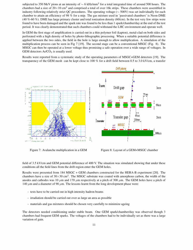
In GEM the first stage of amplification is carried out in a thin polymer foil (kapton), metal-clad on both sides andperforated with a high density of holes by photo-lithographic processing. When a suitable potential difference isapplied between the two sides, the field in the hole is large enough to allow multiplication. A simulation of themultiplication process can be seen in Fig 7 [19]. The second stage can be a conventional MSGC (Fig. 8). TheMSGC can then be operated at a lower voltage thus promising a safe operation over a wide range of voltages. InGEM detectors Ar/CO2 is usually used.
Results were reported from a systematic study of the operating parameters of MSGC+GEM detectors [19]. Thetransparency of the GEM mesh can be kept close to 100 % for a drift field between 0.5 to 3.0 kV/cm, a transfer
Figure 7: Avalanche multiplication in a GEM Figure 8: Layout of a GEM+MSGC chamber
field of 3.5 kV/cm and GEM potential difference of 400 V. The situation was simulated showing that under theseconditions all the field lines from the drift region enter the GEM holes.
Results were presented from 184 MSGC + GEM chambers constructed for the HERA-B experiment [20]. Thechambers have a size of 30×30 cm2. The MSGC substrate was coated with amorphous carbon, the width of theanodes and cathodes was 10 µm and 170 µm respectively at a pitch of 300 µm. The GEM holes have a pitch of140 µm and a diameter of 90 µm. The lessons learnt from the long development phase were:
- tests have to be carried out in high intensity hadron beams
- irradiation should be carried out over as large an area as possible
- materials and gas mixtures should be chosen very carefully to minimize ageing
The detectors needed conditioning under stable beam. One GEM spark/chamber/day was observed though 3chambers had frequent GEM sparks. The voltages of the chambers had to be individually set as there was a largevariation of gain.
11

Figure 9: X-ray absorption image of a small mammal taken with a double-GEM detector.
MSGC+GEM chambers are being considered for the readout of the TPC in TESLA.
Much research is still being carried out on these miniaturized gas chambers. The introduction of GEM means thatthe effective gain can be adapted to particular needs by having one or more stages of GEM amplification. The bigadvantage is that the gas amplification and read-out stages can be separated. As the signal is induced by the motionof electrons, the probability of discharge is almost eliminated. As an example, Fig. 9 shows a radiographic imageof a bat taken using a chamber comprising a double GEM with 2-D readout [21].
5 CalorimetryConsiderable research was carried out to select and then develop the electromagnetic calorimeters of the LHC ppexperiments. ATLAS chose liquid argon sampling calorimeter for the electromagnetic calorimeter and the endcaphadronic calorimeter. CMS chose lead tungstate scintillating (PbWO4) crystals for its electromagnetic calorimeter.Both experiments use scintillator based hadronic calorimeters with wave-length shifting fibres.
5.1 ATLAS Accordion Liquid Argon Sampling Electromagnetic Calorimeter
Conventionally the absorber planes in ionization chambers are oriented perpendicular to the incident particles.However in geometry it is difficult to
• realise fine lateral segmentation with small size towers, which in addition need to be projective in colliderexperiments,
• implement longitudinal sampling,
without introducing insensitive regions, a large number of penetrating interconnections, and long cables whichnecessarily introduce electronics noise and lead to increased charge transfer time. To overcome these shortcomingsa novel absorber-electrode configuration, known as the ’accordion’ (Fig. 10, [22]), has been introduced, in whichthe particles traverse the chambers at angles around 450. With such structures the electrodes can easily be groupedinto towers at the front or at the rear of the calorimeters.
In ATLAS ECAL the absorber is made of lead plates, clad with thin stainless steel sheets for structural stiffnessand corrugated to the shape shown in Fig. 11. Details of the sampling structure can also be seen. The read-outelectrodes are made out of copper clad kapton flexible foil and kept apart from the lead plates by a honeycombstructure.
Results from a full-size barrel prototype module were presented. The final functionality electronic readout chainwas employed but not in the radiation-hard version. The local energy resolution for electrons could be parametrizedby
σ(E)/E = (9.18± 0.13)% /√
E ⊕ (0.27± 0.04)% (2)
where E is in GeV. The e/µ ratio is measured to be 0.75 ± 0.03. The photon-pointing resolution, necessary tomeasure direction of photons from the H → γγ decay, was measured to satisfy the requirement of 50mrad/
√E.
12

Figure 10: A view of the ATLAS Barrel Module 0 liquid argon “accordeon” calorimeter wedge
5.2 ATLAS Endcap Liquid Argon Hadronic Calorimeter
The ATLAS endcap hadronic calorimeter has a conventional structure but for a novel readout that employs 3readout electrodes/gap linked serially, in an approach termed ’electrostatic transformer structure’. Copper plates,with a thickness of 25mm and 50 mm, sandwich argon gaps of a width of ∼ 8 mm. Several modules of HEC weretested [22]. The energy resolution could be parametrized by
σ(E)/E = (70.6 ± 1.5)% /√
E ⊕ (5.8 ± 2.2)% (3)
The e/µ ratio is measured to be 0.93 ± 0.04. The e/h ratio was measured to be 1.5 ± 0.02. The series productionof both the electromagnetic and hadronic modules is well underway.
6 PhotodetectorsThe parallel session had many presentations on developments of photodetectors.
6.1 Silicon Avalanche Photodiodes and Vacuum Phototriodes
The electromagnetic calorimeter for CMS uses lead tungstate (PbWO4) scintillating crystals as the active medium.In many respects PbWO4 is an ideal crystal for use at the LHC. It has:
- a very short radiation length (8.9 mm) and Moliere radius (21.9mm) allowing a compact design
- fast scintillation emission (> 90 % of the light emitted within 100 ns) in the visible region (∼ 430 nm)
- strong resistance to radiation induced darkening
However the light yield is rather low (∼ 50 photons/MeV) necessitating the use of photodetectors with internalgain. Furthermore, in CMS the ECAL is located in a solenoidal magnetic field of 4T. Therefore photodevices thatcan provide some gain and operate in a magnetic field are required. The photodetectors chosen in the barrel areavalanche photodiodes [23]. In the endcap the radiation levels are much higher than in the barrel and the use ofsilicon based photodetectors such as APDs is excluded: vacuum phototriodes are used in this region [24]. Theintegrated radiation levels over 10 years of LHC operation in the barrel part of CMS are 2.1013 n/cm2 and 2.5 kGywhilst in the endcap region, and |η|=2.6, the levels are 1014 n/cm2 and 25 kGy.
13

6.1.1 Avalanche Photodiodes (APDs)
APDs are novel devices; only a handful were available in the early 1990’s. CMS will use 120,000 devices (2 percrystal) [23]. CMS has developed these APDs over 8 years in close collaboration with Hamamatsu. The structureof these APDs is shown in Fig. 11. Incident photons produce photoelectrons in the surface layers (∼ 5 µm thick)that are accelerated in the high field region of the p-n junction. They gain enough energy to create further electron-hole pairs and an avalanche is generated. The diode structure is embedded in ∼ 40 µm of eptaxially grown siliconon a low resitivity silicon base. The grooves etched around the edges reduce surface currents and are important forradiation hardness. Some important characteristics of APDs are listed in Table 6.
Table 6: Some important characteristics of APDs.
Active area (2 APDs/crystal) 5 × 5 mm (each)Quantum efficiency 75 % at 430 nmOperating voltage ∼ 380 V
Gain (M) 50 (max > 1000)Capacitance 80 pF
Voltage sensitivity (1/M × dM/dV) 3.15 % / VTemperature sensitivity (1/M × dM/dT) - 2.2 % / 0C
Excess noise factor 2.1Thickness sensitive to ionizing particles 5 µm
Amongst the improvements made in the course of this development are:
- the amplification region has been placed just behind the conversion layer to substantially decrease the sensi-tivity to traversing charged particles.
- the epitaxial layer is grown on a few hundred microns thick low resistivity silicon to lower the capacitance
- the tolerance to radiation has been improved after changing the geometry to reduce lateral electric field, byrounding corners, changing spacings and introducing field clamps.
Radiation hardness proved to be hard to assure. An important indicator of radiation hardness was found to be thedifference between the breakdown (VB) and operating voltages (VC) (the difference (VB-VC) for good APDs is∼ 40V).
Since the aim is to reach a failure rate of only 0.1 % over 10 years of LHC operation all APDs will be screenedby non-destructive irradiation at 5 kGy with 60Co. This will be followed by 2 weeks of annealing and acceleratedageing at 900C to remove all the dark current induced by the irradiation. Any APD showing a large VB-VC oran anomalously large leakage current will be rejected. Destructive tests with neutron irradiation have also beencarried out. Some 500 screened APDs have been irradiated without any failure.
Around twenty thousand APDs have already been delivered to CMS.
6.1.2 Vacuum Phototriodes (VPTs)
A vacuum phototriode is essentially a photomultiplier tube with a single stage of gain (Fig. 12 [24]). After emissionfrom the photcathode the photolelectrons are accelerated towards the anode consisting of a very fine metal mesh. Afraction (∼ 50 %) of the photons pass through the anode and strike a solid metal dynode, located behind the anode.Secondary electrons ejected from the dynode are accelerated back towards the anode where most are collected.Under normal operating conditions (VA=1000V, VD=800V) the effective gain of the VPT is ∼ 10.
In CMS, the angle between the axis of the VPT and the direction of the magnetic field will vary from ∼ 60 to 260.It has been verified that the gain of the VPT does not vary by more than 10 % in the range of angles from -300 to+300.
Radiation hardness is an issue because radiation can cause darkening of the window due to the formation of colourcenters. Tubes with a standard borosilicate window are readily darkened by radiation. Tubes with fused silicawindows are tolerant but would be prohibitively expensive for application in CMS. The use of UV transmittingglass is a good compromise that shows a small loss of transmission (∼ 4 %) at the doses mentioned above.
14

= 26.5 mm
MESH ANODE
Figure 11: Schematic of an APD Figure 12: Schematic of a VPT
6.1.3 Visible Light Photon Counter (VLPC)
A novel item of the D0 upgrade is the scintillating fibre tracker employing 77,000 fibres, with a diameter of835-µm, arranged in axial and u,v steros doublets. The light is detected by a solid state device developed byRockwell called the visible light photon counter (VLPC) [25]. The incoming photon is converted in the intrinsicregion creating an electron-hole pair. The hole drifts into the drift region where it ionizes an atom. The electronis accelerated back through the gain region generating avalanche amplification. Gains of 20,000 to 60,000 canbe attained. These devices have high quantum efficiency (80 % in the visible). The single photon response isexcellent. An inconvenience of these devices is the need to run at 7 K. In D0 each scintillating fibre is connectedto a 7-11 m long clear fibre that transmits the light to the VLPCs kept in a dewar outside the experiment.
6.1.4 Hybrid Photodiodes (HPDs)
HPDs are two stage vacuum devices: photons are converted in a conventional photocathode and the photoelectronsare accelerated in an electric field of 10 kV/cm. The energetic photoelectrons then strike a silicon detector that actsas an anode. Electron-hole pairs are created (one per 3.7 eV of deposited energy) resulting in a gain of the order of3000. These photodevices can operate in axial magnetic fields. The single photoelectron response of such devicesis excellent as can be seen from Fig. 13 [26]. At LHC they are used to detect light from the scintillators of theCMS HCAL and to detect Cerenkov photons from the LHCb RICH [27].
CMS uses commercially manufactured 19 pixel channel devices in a standard 2’ envelope. Results were presentedin this conference from tests of specially prepared HPDs, used to detect light from an aerogel Cerenkov radiator[27]. Four HPDs with pixelised readout consisting of 2048 channels were used. The fountain shaped electric fieldgives a 2.4 fold de-magnifed image. The separation of proton / pion rings produced by a beam of 8 GeV/c is shownin Fig. 14.
7 Muon ChambersPerhaps the biggest challenge for the measurement of momentum and identification of muons in the LHC ppexperiments is the manufacture of thousands of m2 of chambers with the desired high precision (as low as 80 µmper measured point) and including alignment procedures able to maintain such accuracy over large surface areas.These chambers use technologies that are not necessarily novel. However, much R&D was required to demonstratethe required rate capability and good long-term operation under the modest levels of radiation anticipated in theseregions.
For precision measurements both ATLAS and CMS use drift devices in the barrel region (Drift Tubes (DTs) andMonitored Drift Tubes (MDTs) respectively) and Thin Gap Chambers (TGCs) and/or Cathode Strip Chambers(CSCs) in the endcap regions. Both experiments use Resistive Plate Chambers (RPCs) for precise timing andtriggering. CMS also uses the precision chambers for triggering.
15
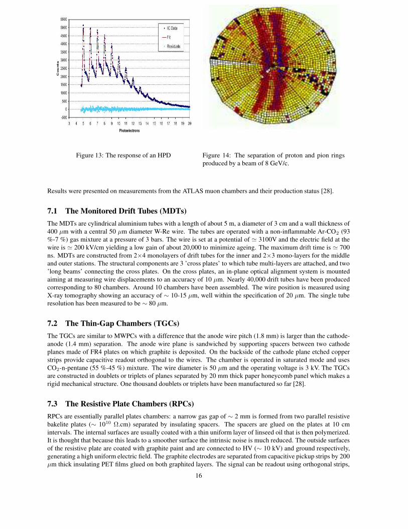
Figure 13: The response of an HPD Figure 14: The separation of proton and pion ringsproduced by a beam of 8 GeV/c.
Results were presented on measurements from the ATLAS muon chambers and their production status [28].
7.1 The Monitored Drift Tubes (MDTs)
The MDTs are cylindrical aluminium tubes with a length of about 5 m, a diameter of 3 cm and a wall thickness of400 µm with a central 50 µm diameter W-Re wire. The tubes are operated with a non-inflammable Ar-CO2 (93%-7 %) gas mixture at a pressure of 3 bars. The wire is set at a potential of ' 3100V and the electric field at thewire is ' 200 kV/cm yielding a low gain of about 20,000 to minimize ageing. The maximum drift time is ' 700ns. MDTs are constructed from 2×4 monolayers of drift tubes for the inner and 2×3 mono-layers for the middleand outer stations. The structural components are 3 ’cross plates’ to which tube multi-layers are attached, and two’long beams’ connecting the cross plates. On the cross plates, an in-plane optical alignment system is mountedaiming at measuring wire displacements to an accuracy of 10 µm. Nearly 40,000 drift tubes have been producedcorresponding to 80 chambers. Around 10 chambers have been assembled. The wire position is measured usingX-ray tomography showing an accuracy of ∼ 10-15 µm, well within the specification of 20 µm. The single tuberesolution has been measured to be ∼ 80 µm.
7.2 The Thin-Gap Chambers (TGCs)
The TGCs are similar to MWPCs with a difference that the anode wire pitch (1.8 mm) is larger than the cathode-anode (1.4 mm) separation. The anode wire plane is sandwiched by supporting spacers between two cathodeplanes made of FR4 plates on which graphite is deposited. On the backside of the cathode plane etched copperstrips provide capacitive readout orthogonal to the wires. The chamber is operated in saturated mode and usesCO2-n-pentane (55 %-45 %) mixture. The wire diameter is 50 µm and the operating voltage is 3 kV. The TGCsare constructed in doublets or triplets of planes separated by 20 mm thick paper honeycomb panel which makes arigid mechanical structure. One thousand doublets or triplets have been manufactured so far [28].
7.3 The Resistive Plate Chambers (RPCs)
RPCs are essentially parallel plates chambers: a narrow gas gap of ∼ 2 mm is formed from two parallel resistivebakelite plates (∼ 1010 Ω.cm) separated by insulating spacers. The spacers are glued on the plates at 10 cmintervals. The internal surfaces are usually coated with a thin uniform layer of linseed oil that is then polymerized.It is thought that because this leads to a smoother surface the intrinsic noise is much reduced. The outside surfacesof the resistive plate are coated with graphite paint and are connected to HV (∼ 10 kV) and ground respectively,generating a high uniform electric field. The graphite electrodes are separated from capacitive pickup strips by 200µm thick insulating PET films glued on both graphited layers. The signal can be readout using orthogonal strips,
16

enabling 2-D position measurement. The chambers have a good time resolution (∼ few ns) and the signal durationis short (< 25 ns).
RPCs can be operated both in the avalanche mode and streamer mode. The avalanche mode offers a higher ratecapability and stable timing performance that is independent of counting rate and is the mode suitable for operationat the LHC. In ATLAS the gas mixture used is tetrafluoroethane (C2H2F4), a non-flammable and environmentallysafe gas, and ∼ 3 % iso-butane (C4H10); 0.3 % SF6 may be used to suppress streamer formation. At ∼ 10kV thestreamer probablility is about 0.1 % and the rate capability is expected to be up to 1 kHz/cm2.
Considerable attention has recently been paid to RPCs due to the experience of BaBar where the oiled RPCs, runin streamer mode, showed significant ageing. Significant and continued efficiency drop was observed even afterincreasing the bias voltage. Some of the affected chambers were opened and oil droplets were found instead of asmooth surface. A new oil treatment is now employed: a ’diluted’ mixture of 60 % (instead of 40 %) eptane/linseedoil is used and a single pass (instead of 3) is made resulting in thinner coating (∆t ∼ 10 µm instead of ∼ 100 µm).Furthermore smoother bakelite plates are now used. Much effort has also been put into quality control proceduresat the gap fabrication plant. It is now believed that these chambers should not age.
A 15-month ageing test has been performed at CERN-X5 GIF irradiation facility. After 0.3 C/cm2, correspondingto 10 ATLAS LHC years, the tested RPC still had a rate capability of 200-300 Hz/cm2 [28].
Results were reported at this conference on chambers operated in the streamer mode [29]. Prototypes with ’diluted’oil coating were subjected to 2 months of irradiation in GIF at a rate between 5-150 Hz/cm2. Ageing was not foundto be dramatic and double coating seemed to be more resistant to ageing!
CMS has been developing uncoated RPCs by smoothing the bakelite surfaces before assembly. Although many ofthe operating specifications can be met one has caused some concern. Un-oiled chambers have a higher intrinsicnoise rate: some 10 times that from an oiled chamber. In CMS this causes a high trigger rate that does not allow asufficient margin for unforeseen problems. As a consequence CMS will also oil the chambers in the barrel region.
A major production run of RPCs, for both CMS and ATLAS, will take place soon with increased emphasis onquality control and monitoring of the oiling step. Initially every tenth chamber will be opened for inspection of thepolymerized oiled-surfaces.
Within CMS, R&D is still being carried out to reduce the intrinsic noise of un-oiled chambers. For example, theintrinsic noise is found to decrease by a factor of three when the graphite coating is offset from the edge of thebakelite plate by 3 cm instead of the usual 1.5 cm. In the endcap region the neutron-induced noise rate (due togammas from n-capture reactions) is similar or higher than the intrinsic one and un-oiled chambers in this regionwould be preferred, as long-term ageing in a high radiation environment is still a concern.
8 ElectronicsThe subject of the electronics tends to be overlooked in such presentations. In the current large-scale experimentsaround one-third of the cost of the sub-detectors resides in electronics. In the harsh environment of the LHC therisks to the proper functioning of the detector-system are considerably higher than this cost percentage. All theelectronics inside the experimental caverns of LHC pp experiments has to be rad-tolerant whereas those in thehigh radiation environment (inner tracker, ECAL etc.) have to be radiation-hard. These requirements pose newchallenges for HEP experiments. This, together with the development of advanced microelectronics technologyhas meant that an unusually large fraction of the electronics has had to be custom-designed.
The line width found in microelectronics circuits has been decreasing exponentially with time over the last thirtyyears; it has decreased in commercial circuits from 2 µm in 1985 to 0.25 µm in 2000. This has meant that the costper/channel could be lowered and larger and larger number of channels could be envisaged opening the possibilityof building better performing detectors. There has been an almost exponential increase in the number of channelsper experiment (Fig. 15) although the experiments themselves have become bigger as well!
In the last decade considerable effort has gone into designing highly performing, low power consuming, lowcost/channel and radiation-hard electronics. For most of the last decade electronics designers had worked withfoundries traditionally supplying radiation-hard electronics to defence and space applications. The up-front costshave been high, and the turn-around times long, hampering rapid development. More recently, as the line widthhas decreased, deep sub-micron technologies, with some modification, have been found to satisfy the radiationhardness requirements. Most of the R&D for the LHC pp experiments has been completed and the productionphase is being entered.
17

100
101
102
103
104
105
106
107
No of electronic channels
2010200019901980
Year of operation
Channels
VLSI chips
Discrete
circuits
Custom VLSI circuits
64-128 channels/chip
Figure 15: The evolution of the number of electronic channels and chips used in experiments.
To illustrate the above mentioned requirements and developments we take, as an example, the electronics chain ofthe CMS tracker. On the Si detector each microstrip is read out by a charge sensitive amplifier with τ ∼ 50ns. Theoutput voltage is sampled at the beam-crossing rate of 40 MHz. The samples are stored in an analog pipeline upto the Level-1 trigger latency (3.2 µs). Following a trigger a weighted sum of 3 samples is formed in an analogcircuit. This confines the signal into single bunch crossing and gives the pulse height. The buffered pulse heightdata are multiplexed out on optical fibres. The output of the laser is modulated by the pulse height for each strip.The light pulses are transported via 120 m long optical fibres to the underground control room that is accessibleduring data taking. The light signal is converted into an electrical signal by Si photodiodes and digitized to givethe pulse height. After zero-suppression and formatting the data are stored in local memories ready for access bythe DAQ system. Unlike most previous experiments, the functions up to and including light transmission into theoptical fibre, are carried out in custom-designed radiation-hard electronics. It should be noted that most of the dataof the LHC pp experiments will be transported out on optical fibres. Installation and commissioning of such a largeoptical cable plant will be a challenge in its own right!
The design of the CMS tracker front-end chip (APV) was almost finalized in 1997 and found to satisfy theradiation-hardness specification. However the vendor decided to carry out the production in a newly set-up foundryand the extreme radiation hardness requirements could no longer be met. As force − majeure CMS decided toinvestigate a path that looked promising utilizing a foundry that mass-produced chips in 0.25 µm CMOS pro-cess (’deep-submicron’ process). Many radiation-hard circuits for the LHC experiments have been, or are being,converted into this technology. We consider below the reasons why [30, 31].
Radiation effects can be divided into two categories: total dose effects and single event effects [30]. Total doseeffects in CMOS are mainly associated with charging-up of oxides. During irradiation electrons and holes aregenerated in the oxides. While the electrons are evacuated rapidly (within ns) holes accumulate in traps leadingto transistor threshold shifts. As the oxides get thinner the charging decreases in proportion to the volume of theoxide. Hence thinner oxides are inherently more radiation hard. As the oxide thickness falls below 10 nm thereduction in the radiation induced threshold voltage becomes even more pronounced. It is thought that electronsthat tunnel into the oxide combine with radiation induced trapped holes. Therefore for deep sub-micron processes(a 0.25 µm process has a gate oxide thickness of 5 nm) radiation induced threshold voltage shift becomes negligibleeven at very high radiation doses. However there is still the possibility of leakage paths from drain to source and
18

from one transistor to another that have to be eliminated by special layout techniques [32].
Single event effects are also important especially for the inner trackers at the LHC. These are considered in orderof severity.
Single event gate rupture (SEGR) is a catastrophic breakdown of transistor gate that occurs when a highly ionizingparticle induces an avalanche breakdown of the gate oxide. Fortunately the effect only manifests itself above acritical threshold electric field and should not be an issue for deep sub-micron CMOS circuits.
Single event latch-up (SEL) occurs when a highly ionizing particle deposits enough charge in a small volume ofthe Si substrate to switch on a parasitic thyristor that causes a very high current to flow between power supplies.If this current is not detected quickly and the power supplies interrupted the chip may be destroyed. One way ofavoiding SEL is to use guard rings and substrate contacts extensively in the design. Fortunately these are also thedesign techniques used to limit total dose effects mentioned above. The 0.25 µm components have been tested toa LET of 89 MeV cm2 mg−1.
Single event upsets (SEU) occur when highly ionizing particle deposits charge near a low capacitance node causingthe logical level of the node to switch state. This effect occurs above a threshold LET. The threshold LET tends todecrease for smaller feature sizes and is a real concern for deep sub-micron circuits.
In the 1999 edition of the roadmap of the Semiconductor Industry Association gate lengths are predicted to fallfrom the present-day 180 nm to 35 nm by 2014 accompanied by a fall in the power supply from the present 1.8V to 0.6 V. The shrinking of the transistor dimensions should enable continuation of the exponential increase incomponent density with time. Understanding the limits, and applicability, of such electronics should be a subjectof vigorous R&D in our field for the next generation of experiments and for the upgrades of LHC experiments.
The response function of the CMS-APV25 0.25 µm chips is unchanged for doses up to 20 Mrads. These chips havebeen coupled to final Si modules and have yielded the expected performance: S/N of ∼ 15 in the de-convolutionmode. The final chip, with a size of ∼ 7 × 8 mm2, was received in August 2000. Following these technologydevelopments has resulted in electronics that have lower cost, have lower noise, are made in foundries catering forvolume rather than niche markets which has resulted in a faster turnaround from design to working chips.
9 Future ChallengesExtreme performance requirements invariably force the pace of detector development. The requirements for theLHC experiments have been a supreme example of this. The linear collider experiments will necessarily pushthe limits of pixel detectors and high granularity dense calorimetry. Upgrading the LHC to attain luminositiesof 1035 cm−2s−1 is already being discussed. This will require further R&D especially for the inner trackingdetectors (monolithic pixel detectors, macro-pixel detectors, use of defect engineered silicon, Si detectors withnovel biasing schemes, Si detectors run at cryogenic temperatures, new sensor materials, engineering issues), forthe associated electronics (10-fold increase in number of channels at 10 times lower cost per channel, radiationhardness of electronics at tens of nm feature size), for higher bandwidth optical links for data transport (10 Gbit/s)with rad-hard transmitter end etc.
10 ConclusionsIt is clear that much progress has been made in detector development in the last decade. This has been drivenby the physics goals of the LHC experiments. These experiments have now moved into almost industrial-scalemass production. An important lesson being learnt is the importance of putting enough thought, early enough, intothe systems aspects. The new generation of experiments will reap many of the benefits from the R&D that hasbeen necessary for LHC experiments. It is important to acknowledge that improvement of existing techniques andmeasurements and search for novel ones of are essential in the exploration of uncharted science. It is thereforeessential to continue funding of detector (and accelerator) R&D even at a modest level.
11 AcknowledgementsWe would like to thank the organizers of this conference for their hospitality and help. We would like to thank allthe speakers in the parallel session 13 for illuminating talks and providing beforehand electronic copies of theirtransparencies. Austin Ball and Peter Sharp are thanked for commenting on the manuscript. Sasha Nikitenko isthanked for help in preparing this manuscript and Guy Martin for drawing some of the figures.
19
References[1] The CMS Electromagnetic Calorimeter Project, Technical Design Report, CERN/LHCC 97-33, Dec. 1997
[2] A. Annenkov et al., to be submitted to Nucl. Instr. and Meth. A and references therein.
[3] M. Doucet, these proceedings.
[4] K. Honscheid, these proceedings.
[5] http://cmsdoc.cern.ch/cms/TDR/MAGNET/magnet.html
[6] C. Damerell et al., IEEE Trans. Nucl. Sci., 33 (1986) 51.
[7] T. Abe, Proc. Workshop on Vertex Detectors (VERTEX 99), Netherlands, June 1999.
[8] M. Winter, these proceedings.
[9] http://cmsdoc.cern.ch/TDR/TRACKER/tracker.html
[10] D. Pitzl et al., Nucl. Instr. And Meth. A311 (1992) 98.
[11] R. Wunstorf et al., Nucl. Instr. And Meth. A315 (1992) 149.
[12] K. Gill et al., Nucl. Instr. And Meth. A322 (1992) 177.
[13] http://cmsdoc.cern.ch/cms/TDR/TRACKER/tracker-addendum.pdf
[14] J. Libby, these proceedings.
[15] G. Hall, private communication.
[16] A. Oed, Nucl. Instr. And Meth. A263 (1988) 351.
[17] F. Sauli, Nucl. Instr. And Meth. A386 (1997) 531.
[18] R. Bellazzini et al., Nucl. Instr. And Meth. A??? (2000) ???.
[19] G. De Lentdecker, these proceedings.
[20] T. Zeuner, these proceedings.
[21] S. Bachmann et al., Proc. Vienna Conf. on Instrumentation., Feb 2001, Elsevier.
[22] L. Neukermans, these proceedings.
[23] Q. Ingram, these proceedings.
[24] R. Brown, these proceedings.
[25] M. Abolins, these proceedings.
[26] D. Britton, private communication.
[27] M. Calvi, these proceedings.
[28] K. Ishii, these proceedings.
[29] A. Ferretti, these proceedings.
[30] A. Rivetti, 5th Workshop on Electronics for LHC Experiments, CERN 99-09, (1999) 157
[31] M. Campbell et al., Nucl.Instr. and Meth. A 473(2001) 140
[32] P. Jarron et al., Nucl. Phys. B. Proc. Suppl 78 (1999) 625.
20