common-base configuration (cb) the cb configuration having ... 1/part4.pdf · common-base...
TRANSCRIPT

114
Common-Base Configuration (CB)The CB configuration having a low input and high output impedance and a current gain less than 1, the voltage gain can be quite large, ro in MΩ so that ignored in parallel with RC
Fig6-22 CB configuration Fig6-23 re equivalent circuitZi
[6-54]Zo
[6-55]Av
[6-56]Ai Assuming RE >> re
[6-57]
Phase Relationship: the resulting equation for the Av is a positive reveals that the output Vo
and input Vi are in phase for the common-base configuration
Example 8: For the network in fig 6-24
Fig6-24 Ex 8Solution: IE

115
re
Zi
Zo
Av
Ai
Collector Feedback Configuration (CEA feedback path from collector to base increased the stability of the system
Fig6-25 feedback configuration Fig6-26 re model into network of fig6-25Zi

116
[6-58]
Zo to define Zo set Vi to zero , the effect of βre is removed and RF appears in parallel with RC
[6-59]
Av at node C of Fig 6-26
[6-60]
Ai Applying KVL around the outside network loop

117
Ignoring βre compared to RF and βRC gives us
[6-61]βRC >> RF
[6-62]
Phase Relationship: the negative sign in the resulting equation for the Av reveals that a 180 º phase shift occurs between the output VO and input Vi
Example 9: For the network of fig6-27 determine
Fig6-27 Example 9:Solution:IB
IE
re
Zi
Zo
Av
Ai

118
For the configuration of Fig6-28, will determine the variables
Fig6-28 Collector feedback configuration Zi
[6-63]Zo
[6-64]Av
[6-65]
Ai
[6-66]
Collector DC feedback Configuration (CE)The dc feedback resistor increased stability; C3 will shift portions of the feedback resistance to the input and output sections of the network in the ac domain.
Fig6-29 Collector dc feedback Fig6-30 re equivalent circuit of the networkZi
[6-67]Zo
[6-68]For ro ≥ 10RC

119
[6-69]Av
[6-70]For ro ≥ 10RC
[6-71]Ai for the input side
[6-72]
[6-73]
Or [6-74]
Phase Relationship: the negative sign in the resulting equation for the Av reveals that a 180º phase shift occurs between the output VO and input Vi

120
Example 10: For the network of fig6-31 determine:
Fig6-31 Example 10Solution: DC testing:IB
IE
re
βre
Zi
F ig6-32 re equivalent
Testing the condition ro ≥ 10RC we find
It is satisfied So Zo
121
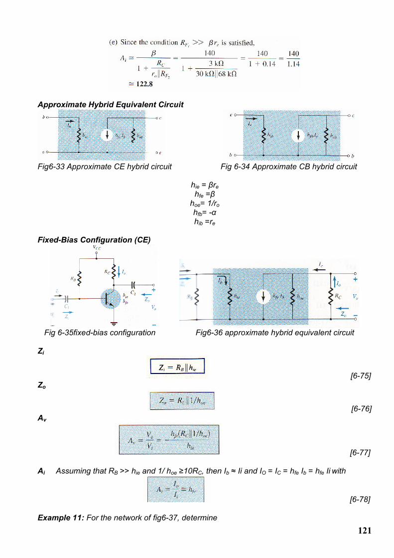
Approximate Hybrid Equivalent Circuit
Fig6-33 Approximate CE hybrid circuit Fig 6-34 Approximate CB hybrid circuit
hie = βre
hfe =βhoe= 1/ro
hfb= -αhib =re
Fixed-Bias Configuration (CE)
Fig 6-35fixed-bias configuration Fig6-36 approximate hybrid equivalent circuit
Zi
[6-75]Zo
[6-76]Av
[6-77]
Ai Assuming that RB >> hie and 1/ hoe ≥10RC, then Ib ≈ Ii and IO = IC = hfe Ib = hfe Ii with
[6-78]
Example 11: For the network of fig6-37, determine

122
Fig6-37 Example 11:Solution:
Voltage-Divider Configuration (CE bypassed)
Fig6-38Voltage-dividerbiasconfigurationZi RB=R'
[6-79]Zo
[6-80]Av
[6-81]Ai
[6-82]
Unbypassed Emitter-Bias Configuration (CE)βre replaced by hie and βIb by hfeIb . The analysis will proceed in the manner

123
Fig6-39 CE unbypassed emitter-bias configurationZi:
[6-83]
[6-84]Zo
[6-89]
Av
And [6-90]
Ai
[6-91]
or [6-92]
Emitter-Follower Configuration (CE)βre = hie and β = hfe , the resulting equations will therefore be quite similar.
Fig6-40Emitter-follower configurationZi
[6-93]

124
[6-94]
Zo the output network will appear as shown in fig
[6-95]Av
[6-96]Ai
[6-97]
or [6-98 ]
Common-Base Configuration (CB)
Fig6-41 CB configuration
Fig6-42 CB hybrid equivalent circuit
Zi
[6-99]Zo
[6-100]

125
Av
[6-101]Ai
[6-102]
Example 12: For the network of fig6-43, determine:
Fig 6-43 Example 12Solution;
126
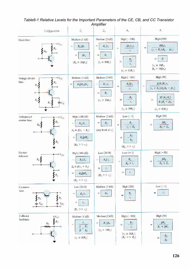
Table6-1 Relative Levels for the Important Parameters of the CE, CB, and CC Transistor Amplifier
127
SUMMARYImportant Conclusions and Concepts1. The re model for a BJT in the ac domain is sensitive to the actual dc operating conditions of the network. This parameter is normally not provided on a specification sheet, although hie of the normally provided hybrid parameters is equal to β re but only under specific operating conditions.
2. Most specification sheets for BJT include a list of hybrid parameters to establish an ac model for the transistor. One must be aware, however, that they are provided for a particular set of dc operating conditions.
3. The CE fixed-bias configuration can have a significant voltage gain characteristic, although its input impedance can be relatively low. The approximate current gain is given by simply beta, and the output impedance is normally assumed to be Rc.
4. The voltage-divider bias configuration has a higher stability than the fixed-bias configuration, but it has about the same voltage gain, current gain, and output impedance. Due to the biasing resistors, its input impedance may be lower than that of the fixed-bias configuration.
5. The CE emitter-bias configuration with an unbypassed emitter resistor has a larger input resistance than the bypassed configuration, but it will have a much smaller voltage gain than the bypassed configuration. For the unbypassed or by-passed situation, the output impedance is normally assumed to be simply Rc.
6. The emitter-follower configuration will always have an output voltage slightly less than the input signal. However, the input impedance can be very large, making it very useful for situations where a high-input first stage is needed to "pick up "as much of the applied signal as possible. Its output impedance is extremely low, making it an excellent signal source for the second stage of a multistage amplifier.
7. The common-base configuration has very low input impedance, but it can have a significant voltage gain. The current gain is just less than 1, and the output impedance is simply Rc
8. The collector feedback configuration has input impedance that is sensitive to beta and that can be quite low depending on the parameters of the configuration. However, the voltage gain can be significant and the current gain of some magnitude if the parameters are chosen properly. The output impedance is most often simply the collector resistance Rc
9. The collector dc feedback configuration utilizes the dc feedback to increase its stability and the changing state of a capacitor from dc to ac to establish a higher voltage gain than obtained with a straight feedback connection. The output impedance is usually close to Rc and the input impedance relatively close to that obtained with the basic common-emitter configuration.
10. The approximate hybrid equivalent network is very similar in composition to that used with the re model. In fact, the same methods of analysis can be applied to both models. For the hybrid model the results will be in terms of the network parameters and the hybrid parameters, whereas for the re model they will be in terms of the network parameters and β , re and ro
11. The hybrid model for common-emitter, common-base, and common-collector configurations is the same. The only difference will be the magnitude of the parameters of the equivalent network.

128
12. for BJT amplifiers that fail to operate properly, the first step should to be checking the dc level and be sure that they support the dc operation of the design.
13. Always keep in mind that capacitors are typically open circuits for the dc analysis and operation and essentially short circuits for the ac response
EquationsCE fixed bias:
CE Voltage-divider bias:
CE emitter-bias:
Emitter-follower:
Common-base:

129
Collector feedback:
Collector dc feedback:

130
7-Felid Effect Transistor (FET)BJT is a current-controlled device; that is IB controls IC. The FET is a voltage-controlled device in which the voltage gate VG controls current through the device. FET is a three-terminal device containing one p-n junction built as either a Junction FET (JFET) or a Metal-Oxide Semiconductor FET (MOS-FET). Construction and Characteristics of JFETSJFET is a type of FET that operates with a reverse biased junction to control current in the channel. JFETs either n channel or p channel
Fig7-1 basic structure of the two types of JFET
Fig7-2Water analogy for the JFET control mechanismJFET SymbolsNotice that the arrow on the gate points "in" for n-channel and "out" for-p channel.
Fig7-3 JFET symbols (a) n-channel (b) p-channel
JFET CharacteristicsFirst consider the case where the VGS = 0V fig7-4a as VDD (and thus VDS) is increased from 0V, ID will increase proportionally (Fig7-4b between points A and B), this region is called the ohmic region because VDS and ID are related by Ohm's law.Point B in Fig7-4b ID becomes constant. As VDS increases from point B to point C, the reverse-bias voltage in VGD produces a depletion region large enough to offset the increase in VDS, thus keeping ID relatively constant.Pinch-Off Voltage VP: is the value of VDS at which ID becomes constant and VGS = 0V, a continued increase in VDS above the VP voltage produces a constant drain current IDSS (Drain to Source current with gate sorted)IDSS: is the maximum drain current and is always specified on JFET data sheets, is defined by the condition VGS = 0V and VDS > |VP |Breakdown: occurs at point C when ID begins to increase very rapidly with any further increase in VDS , Breakdown result damage to the device, so JFETs are always operated below breakdown ( between B & C).VGS Controls ID: Connect a bias voltage VGG, as VGS is set to increasingly more negative values by adjusting VGG, ID decreases.

131
Fig 7-4 the drain characteristic curve of a JFET for VGS = 0 V, (pinch-off)
Fig7-5 pinch-off occurs at a lower VDS as VGS is increased to more negative values
Cutoff Voltage VGS(off) : the value of VGS that makes ID approximately zero ,JFET must be operated between VGS = 0V and VGS(off) , for this range of voltage ID will vary from a maximum (IDSS ) to a minimum . VGS(off) & VP are always equal in magnitude but opposite in sign
(a) VGS = 0V, ID = IDSS (b) cutoff (ID = 0A) VGS less than (more negative) VP
(c) ID exists between 0A and IDSS for VGS less than or equal to 0V and greater than the VP
Fig7-6

132
The basic operation of a p-channel JFET is the same as for an n-channel device expect that is requires a negative VDD and a positive VGS.Example 1: JFET in fig VGS(off) = -3.5V & IDSS =6mA. Determine the minimum value of VDD
required putting the device in the constant-current region of operationSolution:
Since VGS(off)=-3.5V, VP=3.5, VDS=3.5V, ID=IDSS=6mA VRD= (6mA) (560Ω) =3.36V
Applying KVL, VDD=VDS+VRD=3.5V+3.36V=6.86V
JFET Input Resistance The input resistance at the gate is very high. JFET data sheets often specify the input resistance by giving a value for the gate reverse current IGSS at a certain VGS
Example2: A certain JFET has an IGSS of 1nA for VGS = -20V, Determine the input resistanceSolution:
Voltage-Controlled ResistorIn ohmic region JFET be employed as a variable resistor whose resistance is controlled by VGS
[7-1]ro is the resistance with VGS = 0V, and rd the resistance at a particular level of VGS
Fig7-7 n-JFET IDSS =8mA & VP=-4VTransistor CharacteristicDerivation: For BJT the output current IC and input controlling current IB related to beta, which was considered constant for the analysis
A liner relationship exist between IC and IB . [7-2]

133
This liner relationship dose not exists between the output and input quantities of the JFET, the relationship between ID and VGS is defined by Shockley's equation:
[7-3]The transfer characteristics defined by Shockley's equation are unaffected by the network in which the device is employed
Fig7-8 obtaining transfer charWhen VGS = 0V, ID = IDSS
When VGS = VP = -4V, ID=0 mA, defining an other point on transfer curve. Applying Shockley's Equation: Eq[7-3]Substituting VGS = 0V gives
[7-4]
[7-5]if we substitute VGS = -1V.
The derivation is quite straightforward and will result in
[7-6]Test Eq[7-6]by finding VGS that will result in a drain current of 4.5mA in fig7-8
134
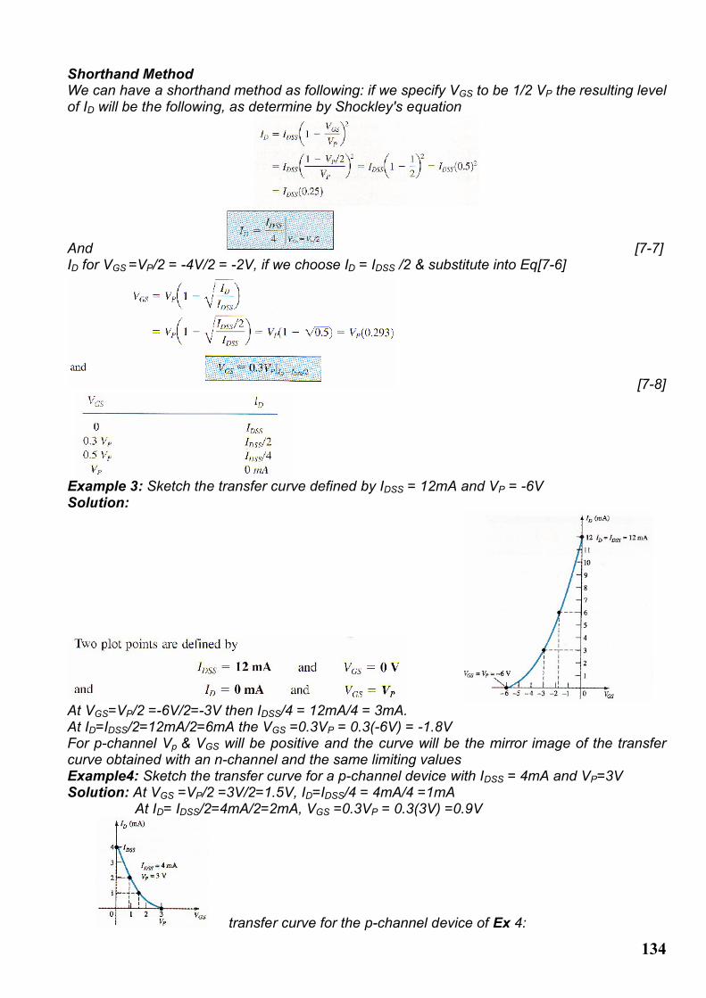
Shorthand MethodWe can have a shorthand method as following: if we specify VGS to be 1/2 VP the resulting level of ID will be the following, as determine by Shockley's equation
And [7-7]ID for VGS =VP/2 = -4V/2 = -2V, if we choose ID = IDSS /2 & substitute into Eq[7-6]
[7-8]
Example 3: Sketch the transfer curve defined by IDSS = 12mA and VP = -6VSolution:
At VGS=VP/2 =-6V/2=-3V then IDSS/4 = 12mA/4 = 3mA.At ID=IDSS/2=12mA/2=6mA the VGS =0.3VP = 0.3(-6V) = -1.8VFor p-channel Vp & VGS will be positive and the curve will be the mirror image of the transfer curve obtained with an n-channel and the same limiting valuesExample4: Sketch the transfer curve for a p-channel device with IDSS = 4mA and VP=3VSolution: At VGS =VP/2 =3V/2=1.5V, ID=IDSS/4 = 4mA/4 =1mA At ID= IDSS/2=4mA/2=2mA, VGS =0.3VP = 0.3(3V) =0.9V
transfer curve for the p-channel device of Ex 4:

135
Important Relationships
Fig7-9 (a) JFET (b) BJT
MOSFET (metal-oxide-semiconductor-field-effect transistor)There is no direct electrical connection between the gate terminal and the channel of a MOSFET; it is the insulating layer of SiO2 in the MOSFET construction that accounts for the very desirable high input impedance of the device,Depletion MOSFET (D-MOSFET)The drain and source are diffused into the substrate material then connected by a narrow channel adjacent to the insulated gate.
Fig7-10 D-MOSFETsThe D-MOSFET called a depletion/enhancement MOSFET, D-MOSFET operates in the Depletion mode when a VGS is negative, Enhancement mode when VGS is a positive voltage.Depletion Mode Visualize the gate as one plate of a parallel plate capacitor and the channel as the other plate.The SiO2 insulating layer is the dielectric. With VGS negative voltage, the negative charges on the gate repel conduction electrons from the channel, leaving positive ions in their place. Thusdecreasing the channel conductivity, The greater the negative voltage (VGS ), the greater the depletion of n-channel electrons, at a VGS(off) the channel is totally depleted and ID is zero. In depletion mode current between drain and source will result from a voltage connected across the drain-source.
(a)Depletion mode VGS negative < VGS(off) (b) Enhancement: VGS positive
Fig7-11n-channel DMOSFET
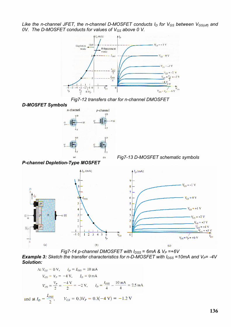
136
Like the n-channel JFET, the n-channel D-MOSFET conducts ID for VGS between VGS(off) and 0V. The D-MOSFET conducts for values of VGS above 0 V.
Fig7-12 transfers char for n-channel DMOSFETD-MOSFET Symbols
Fig7-13 D-MOSFET schematic symbolsP-channel Depletion-Type MOSFET
Fig7-14 p-channel DMOSFET with IDSS = 6mA & VP =+6VExample 3: Sketch the transfer characteristics for n-D-MOSFET with IDSS =10mA and VP= -4VSolution:

137
ID increases very rapidly with increasing positive values of VGS. So that choice values to be substituted into Shockley's equation. In this case, we will try +1V as follows:
n-DMOSFET IDSS = 6mA & VP = -4V
Enhancement Mode With a positive VGS, more conduction electrons are attracted into the channel, thus increasing (enhancing) the channel conductivity, Enhancement MOSFET (E-MOSFET)This type operates only in the enhancement mode and has no depletion mode. It has no structural channel.
Fig7-15E-MOSFET E-MOSFET symbols
For n-channel device, a positive VGS voltage above VGS(off) (threshold voltage)creating a thin layer of negative charges in the substrate region adjacent to the SiO2 layer, the conductivity of the channel is enhanced by increasing the VGS voltage, thus pulling more electrons into the channel. For any VGS voltage below the threshold value, there is no channel.
[7-11]
[7-12]For values of VGS less than the threshold level, ID = 0mA
[7-13]

138
Fig7-16 n-EMOSFET VT=2V&k=0.278x10⁻³ A/V2
[7-14]
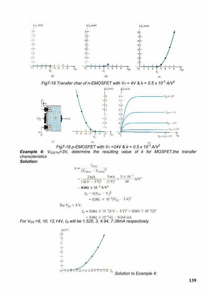
Fig7-17 transfer char- for n-EMOSFET from the drain characteristicsFirst, a horizontal line is drawn at ID =0mA from VGS =0V to VGS =4V as in fig 7-18a next, a level of VGS grater than VT such as 5V is chosen and substituted into Eq.[7-13] to determine the resulting level of ID as follows:
And a point on the plot is obtained as in fig7-18b, finally, additional levels of VGS are chosen and the resulting levels of ID obtained. In particular, at VGS =6, 7, and 8V, the level of ID is 2, 4.5, and 8mA, respectively, as shown on the resulting plot of fig7-18
139
Fig7-18 Transfer char of n-EMOSFET with VT = 4V & k = 0.5 x 10⁻³ A/V2
Fig7-19 p-EMOSFET with VT =24V & k = 0.5 x 10⁻³ A/V2
Example 4: VGS(TH)=3V, determine the resulting value of k for MOSFET,the transfer characteristicsSolution:
For VGS =8, 10, 12,14V, ID will be 1.525, 3, 4.94, 7.38mA respectively.
Solution to Example 4:

140
CMOSCMOS is a complementary MOSFET constructed by a p-channel and an n-channel MOSFET on the same substrate. P-channel on the left and the n-channel on the right
Fig7-20 CMOS connectionsOne very effective use of the CMOS is as an inverter as shown in Fig7-21
Fig7-21 CMOS inverter Fig7-22 resistance levels For Vi = 5 V (1-state)SUMMARY TABLE

141
SUMMARY1. a current controlled device is one in which a current defines the operating condition of the
device, whereas a voltage-controlled device is one in which a particular voltage defines the
operating conditions.
2. Transistors are used as either amplifying devices or switching devices.
3. A field-effect transistor (FET) has three terminals: source, drain, and gate.
4. A junction field-effect transistor (JFET) operates with a reverse-biased gate-to-source pn
junction. JFETs have very high input resistance due to the reverse-biased gate-source
junction.
5. JFET current between the drain and the source is through a channel whose width is
controlled by the amount of reverse bias on the gate-source junction.
6. The two types of JFETs are n-channel and p-channel.
7. The JFET can actually be used as a voltage-controlled resistor because of a unique
sensitivity of the drain-to-source impedance to the gate-to-source voltage.
8. The maximum current for any JFET is labeled IDSS and occurs when VGS =0V.
9. The maximum current for a JFET occurs at pinch-off defined by VGS = VP .
10. The relationship between the drain current and the gate-to-source voltage of a JFET is
nonlinear one defined by Shockley's equation. As the current level approaches IDSS, the
sensitivity of ID to changes in VGS increases significantly
11. The transfer characteristics (ID versus VGS) are characteristics of the device itself and not
sensitive to the network in which the JFET is employed.
12. When VGS = VP/2, ID = IDSS /4; and at a point where ID = IDSS /2, VGS =0.3 V.
13. Maximum operating conditions are determined by the product of the drain-to-source
voltage and the drain current.
14. Metal-oxide semiconductor field-effect transistors (MOSFETs) differ from JFETs in that the
gate of a MOSFET is insulated from the channel.
15. MOSFET is available in one of two types: depletion and enhancement.

142
16. The depletion-type MOSFET has the same transfer characteristics as a JFET for drain
current up to the IDSS level. At this point the characteristics of a depletion-type MOSFET
continue to levels above IDSS, whereas those of the JFET will end
17. A depletion/enhancement MOSFET (D-MOSFET) can operate with a positive, negative. Or
Zero gate-to-source voltage.
18. The D-MOSFET has a physical channel between the drain and the source.
19. The arrow in the symbol of n-channel JFET or MOSFET will always point in to the center of
the symbol, whereas those of a p-channel device will always point out of the center of the
symbol.
20. An enhancement-only MOSFET (E-MOSFET) can operate only when the gate-to-source
voltage exceeds a threshold value.
21. The E-MOSFET has no physical channel.
22. The transfer characteristics of an enhancement-type MOSFET are not defined by
Shockley's equation but rather by a nonlinear equation controlled by the gate-to-source
voltage, the threshold voltage, and a constant k defined by the device employed. The resulting
plot of ID versus VGS is one that rises exponentially with increasing values of VGS.
23. A CMOS (complementary MOSFET) device is one that employs a unique combination of a
p-channel and an n-channel MOSFET with a single set of external leads. It has the advantages
of very high input impedance, fast switching speeds, and low operating power levels, all of
which make it very useful in logic circuits.
EQUATIONS:FET
MOSFET (enhancement):