comparison of planar and toroidal pcb integrated inductors
TRANSCRIPT
HAL Id: hal-01535721https://hal.archives-ouvertes.fr/hal-01535721
Submitted on 9 Jun 2017
HAL is a multi-disciplinary open accessarchive for the deposit and dissemination of sci-entific research documents, whether they are pub-lished or not. The documents may come fromteaching and research institutions in France orabroad, or from public or private research centers.
L’archive ouverte pluridisciplinaire HAL, estdestinée au dépôt et à la diffusion de documentsscientifiques de niveau recherche, publiés ou non,émanant des établissements d’enseignement et derecherche français ou étrangers, des laboratoirespublics ou privés.
Comparison of planar and Toroidal PCB integratedinductors for a multi-cellular 3.3 kW PFC
Rémy Caillaud, Cyril Buttay, Roberto Mrad, Johan Le Lesle, Florent Morel,Nicolas Degrenne, Stefan Mollov
To cite this version:Rémy Caillaud, Cyril Buttay, Roberto Mrad, Johan Le Lesle, Florent Morel, et al.. Comparison ofplanar and Toroidal PCB integrated inductors for a multi-cellular 3.3 kW PFC. 2017 IEEE IWIPP,Apr 2017, Delft, Netherlands. 10.1109/IWIPP.2017.7936757. hal-01535721
Comparison of Planar and Toroidal PCB integrated inductors for amulti-cellular 3.3 kW PFC
Rémy Caillaud1,2, Cyril Buttay2, Roberto Mrad1, Johan Le Lesle1,2, Florent Morel2, Nicolas Degrenne1
and Stefan Mollov1
1Mitsubishi Electric R&D Centre Europe(MERCE)
1 Allée de beaulieu35708, Rennes, France
2Université de LyonINSA Lyon
UMR CNRS 5005, AmpèreLyon, France
Abstract—The Printed-Circuit-Board (PCB) technology is at-tractive for power electronic systems as it offers a low manu-facturing cost for mass production. In this paper, we presenta procedure to design power inductors based on PCB. Theseinductors either use PCB for the winding only (Planar structure),or to host both the magnetic core and the winding (ToroidalPCB structure). The design procedure compares, in the form ofa Pareto fronts, the two inductor structures over a large rangeof parameters (geometric parameters, magnetic materials), toidentify the best candidates in terms of power losses and boxvolume. In this procedure, the core losses are taken into accountusing improved Generalized Steinmetz Equation (iGSE). The skinand proximity effects are considered using the AC resistancecalculated with a FEM software. The inductor feasibility ischecked from a mechanical perspective using the PCB designrules and from a thermal point of view with FEM simulation. Adesign case is presented for a 3.3 kW multi-cellular (3 interleavedcells) Power Factor Corrector (PFC). It is found that the planardesign offers the most compact solution, but might presentchallenges regarding thermal management. The Toroidal PCBstructure tends to be larger, but easier to cool.
I. INTRODUCTION
Although it is a recent technology, embedding of powerelectronic components in Printed Circuit Board (PCB) hasattracted interest from the industry, with products alreadyavailable on the market [1]. This technology enables moreintegrated converters, with a single, consistent manufacturingprocess. PCBs present a low manufacturing cost for massproduction. The passive components represent a large share(20 %) of a converter volume, on par with its cooling systemand empty spaces [2]. Their integration in the PCB is thereforeespecially attractive. However, most studies focused on theintegration of power semiconductor devices only, or on theintegration of passive devices, but for very low power only(for converters with a power under a few tens of watts). Dieembedding technology is commercially available from severalPCB manufacturers (AT&S, ASE, Würth Electronik. . . [3]).Low-power or low-value capacitive devices are formed usingcapacitive layers [4] integrated in the PCB stack-up. Regardingmagnetic devices, the investigations were mainly focused onlow-power application using either no magnetic material atall (“coreless”) [5], or cores with a small size. For example,in [6], two coupled inductors (3 µH each) for a load powerof 30 W are embedded in a PCB of 4.5x4x0.25 = 4.5 cm3.Transformer also can be embedded in PCB, like in [7] in whicha 1.5x2.2x0.36 = 1.18 cm3 - 2 W power supply is prototyped.
VS
L1
VL1
IL1
CO Load
Q1 Q2
Q3 Q4
VDC
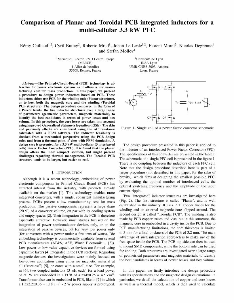
Figure 1: Single cell of a power factor corrector schematic
The design procedure presented in this paper is applied tothe inductor of an interleaved Power Factor Corrector (PFC).The specifications of this converter are presented in the table I.The schematic of a single PFC cell is presented in the figure 1.There is no coupling between the inductors of each PFC cell.Note that the design procedure described here is part of alarger procedure (not described in this paper, for the sake ofbrevity), which aims at designing the smallest possible PFC,by evaluating the optimal number of interleaved cells, theoptimal switching frequency and the amplitude of the inputcurrent ripple.
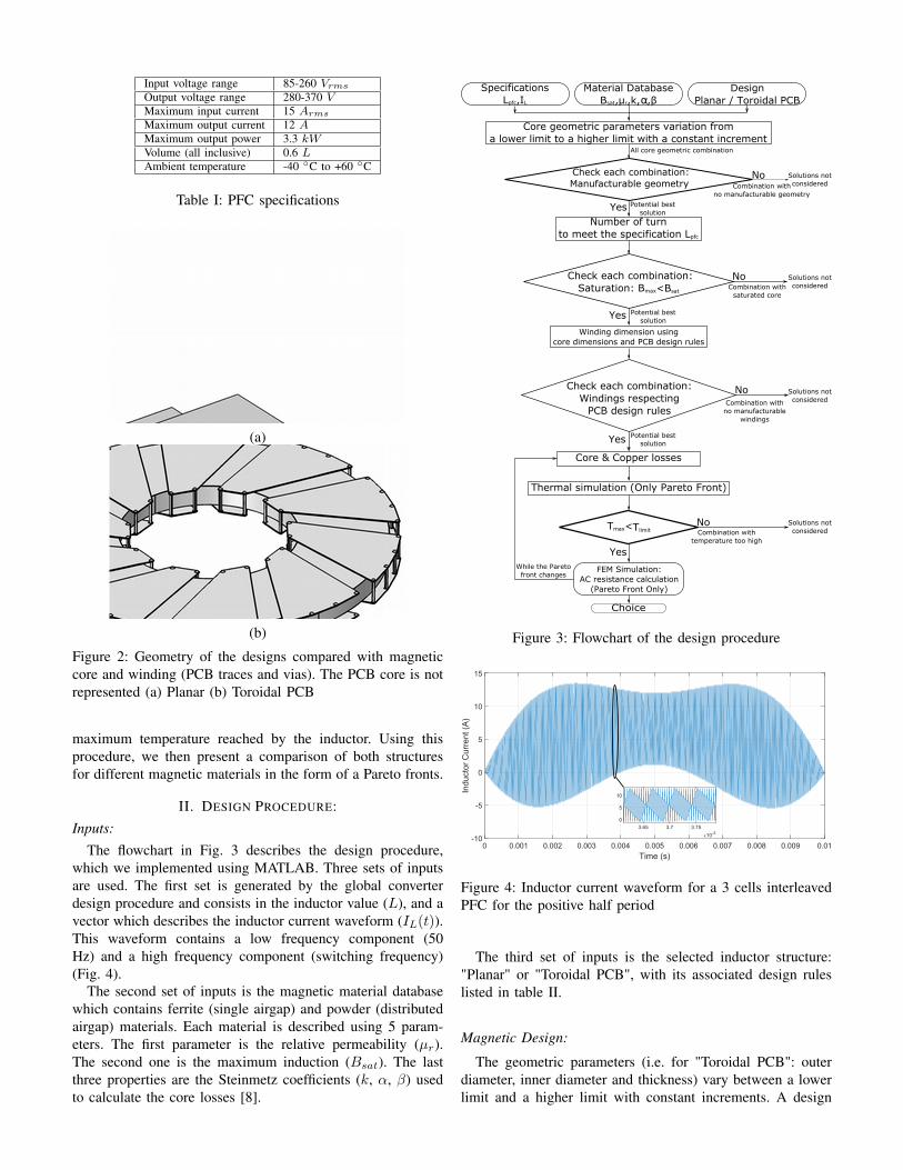
Two “integrated” inductor structures are investigated here(Fig. 2). The first structure is called "Planar", and is wellestablished in the industry. It uses PCB copper traces for thewinding and an external magnetic core clipped around. Thesecond design is called "Toroidal PCB". The winding is alsomade by PCB copper traces and vias, but in this structure, themagnetic core in embedded in a cavity inside the PCB. Due toPCB manufacturing limitations, the core thickness is limitedto 3 mm for a final thickness of the PCB of 3.2 mm. The mainadvantage of such integration approach is to make use of thefree space inside the PCB. The PCB top side can then be usedto mount SMD components, while the bottom side can be usedfor cooling. Both structures are investigated over a large rangeof geometrical parameters and magnetic materials, to identifythe best candidates in terms of power losses and box volume.
In this paper, we firstly introduce the design procedurewith its specifications and the magnetic design calculations. Inparticular, we detail the calculation of copper and core lossesas well as a thermal model, which is then used to calculate
Input voltage range 85-260 Vrms
Output voltage range 280-370 VMaximum input current 15 Arms
Maximum output current 12 AMaximum output power 3.3 kWVolume (all inclusive) 0.6 LAmbient temperature -40 C to +60 C
Table I: PFC specifications
(a)
(b)
Figure 2: Geometry of the designs compared with magneticcore and winding (PCB traces and vias). The PCB core is notrepresented (a) Planar (b) Toroidal PCB
maximum temperature reached by the inductor. Using thisprocedure, we then present a comparison of both structuresfor different magnetic materials in the form of a Pareto fronts.
II. DESIGN PROCEDURE:Inputs:
The flowchart in Fig. 3 describes the design procedure,which we implemented using MATLAB. Three sets of inputsare used. The first set is generated by the global converterdesign procedure and consists in the inductor value (L), and avector which describes the inductor current waveform (IL(t)).This waveform contains a low frequency component (50Hz) and a high frequency component (switching frequency)(Fig. 4).
The second set of inputs is the magnetic material databasewhich contains ferrite (single airgap) and powder (distributedairgap) materials. Each material is described using 5 param-eters. The first parameter is the relative permeability (µr).The second one is the maximum induction (Bsat). The lastthree properties are the Steinmetz coefficients (k, α, β) usedto calculate the core losses [8].
SpecificationsLpfc,IL
Core geometric parameters variation from a lower limit to a higher limit with a constant increment
Material DatabaseBsat,μr,k, ,βα
Design Planar / Toroidal PCB
Check each combination:Manufacturable geometry
Number of turnto meet the specification Lpfc
Check each combination:Saturation: Bmax<Bsat
No
Yes
Winding dimension usingcore dimensions and PCB design rules
Core & Copper losses
Thermal simulation (Only Pareto Front)
FEM Simulation:AC resistance calculation
(Pareto Front Only)
Choice
Tmax<TlimitNo
Yes
All core geometric combination
Combination with no manufacturable geometry
Solutions not considered
Potential best solution
Combination with saturated core
Solutions not considered
Potential best solution
Check each combination:Windings respecting
PCB design rules
Yes
Combination withno manufacturable
windings
Solutions not considered
Solutions not considered
No
Potential best solution
Combination withtemperature too high
Yes
No
While the Pareto front changes
Figure 3: Flowchart of the design procedure
Time (s)0 0.001 0.002 0.003 0.004 0.005 0.006 0.007 0.008 0.009 0.01
Indu
ctor
Cur
rent
(A
)
-10
-5
0
5
10
15
10-33.65 3.7 3.75
0
5
10
X
Figure 4: Inductor current waveform for a 3 cells interleavedPFC for the positive half period
The third set of inputs is the selected inductor structure:"Planar" or "Toroidal PCB", with its associated design ruleslisted in table II.
Magnetic Design:
The geometric parameters (i.e. for "Toroidal PCB": outerdiameter, inner diameter and thickness) vary between a lowerlimit and a higher limit with constant increments. A design

Copper thickness 105 µmPrePreg thickness 200 µmClearance 200 µmVia drill tool diameter 350 µmVia final diameter 250 µm
Table II: PCB design rules used for inductor design
matrix, containing all combinations of magnetic core geo-metric parameters is then generated. The combinations givingimpossible geometries (e.g. inner diameter larger than outerdiameter) are discarded. For each combination, i.e for eachgiven core geometry, the magnetic path length (le) and themagnetic section (Ae) are calculated. They are used with thepermeability of the chosen material to calculate the numberof turns necessary to achieve the specified inductance value,using eq. (1).
L = µ0µrN2Aele
(1)
Some combinations lead to saturation of the magnetic coredue to an excessive number of turns (µ0µrNmaxImax/le >BSat). These solutions are discarded. With the core geometryand the number of turns for each combination, the windingdimensions are calculated. In some cases, it is not possible tocalculate dimensions which meet the design rules (in particularthe clearance between copper tracks). These solutions arediscarded.
Loss Calculation:
The inductor losses can be separated into core losses andcopper losses.
As the inductor current has a complex waveform (a 50Hz sinewave with a superimposed high frequency ripple),the calculation of the core losses is based on the improvedGeneralized Steinmetz Equation (iGSE, eq (2), [8]).
Pvi =1
T
∫ T
0
k1|dB
dt|α(∆B])β−αdt (2)
where:k1 =
k
(2π)α−1∫ 2π
0| cos θ|α2β−αdθ
(3)
where (k, α, β) are the Steinmetz coefficients, B is the fluxwaveform, T is the period of the signal and i is the index of thehysteresis loop. Indeed, the iGSE has to be applied on majorand minor loops. The inductor current waveform presented inFig. 4 generates one major loop per cycle, and many minorloops, which must be identified. Therefore, the flux densitywaveform is separated into two parts: rising & falling. Thescript begins parsing the rising part of the waveform (fromthe global minimum to the global maximum). The data isattributed to the major loop until the first local maximum isreached. The data is then associated with the first minor loopuntil the data goes through a local minimum and comes backto the first local maximum. From this point to the second localmaximum, the data is added to the major loop. At the secondlocal maximum, the second minor loop begins. This procedure
Arbitrary Time Scale1 2 3 4 5 6 7 8
Flu
x (T
)
0.2
0.3
0.4
0.5
0.6
0.7Rising Part
Major LoopMinor Loop 1Minor Loop 2
First local minimum :The first minor loop begins
The signal reached back the value of the first local minium:
the first minor loop ends & themajor loop continues
The second minor loop begins
The second minor loop ends & the
major loop continues
Figure 5: Arbitrary waveform (rising part) split into major andminor loops for core losses calculation
is repeated up to the global maximum. At the global maximum,the falling part begins, and a comparable (albeit inverting localminimums and maximums) procedure starts. The same processis applied to all minor loops to verify the existence of sub-loops. An example of waveform (rising part only) split intomajor and minor loops is presented in Fig. 5. The core powerloss per unit volume is calculated with the equation 4:
Pcore =∑i
PviTiT
(4)
Regarding copper losses, the DC resistance (RDC) of thewinding is calculated using their geometry and the resistivityof copper (17 nΩ.m). The joule losses caused by the 50 Hzfundamental frequency can be calculated as RDCI2rms,LF . Thecalculation of the joule losses for the high frequency ripplerequire an equivalent AC resistance (RAC), which takes intoaccount skin and proximity effects at the switching frequency.As the distribution of the current in the conductor is affectedby the magnetic field in the inductor, there is no analyticalexpression to calculate RAC . 3D finite elements (COMSOL)simulations are used to calculate the factor K defined asRAC/RDC . The total copper losses are then calculated as:
Pcu = RDC .(Irms,LF +K.Irms,HF )2 (5)
With eq. (5), RAC is assumed to be constant for thefundamental frequency of the current ripple and its harmonics.
The COMSOL model (using version 5.2a) is based on themethod described in [9] where each copper track is representedindependently to take into account skin and proximity effect.However, the ripple frequency imposes a fine mesh (50 mi-crons elements) on the PCB tracks and on the vias to observethese effects. Using such a fine mesh over the entire geometrywould require too much memory, due to the large size of thewhole inductor. Instead, the mesh is customized, with differentelements size and type for the envelope of the tracks and forthe rest of the model, to keep it computationally light. Anothersolution to keep the computation time low is to simulate theAC resistance for the inductors which belong to the Paretofront only (for the other inductors, a fixed RAC/RDC ratiois considered). The copper loss are calculated with the newRAC/RDC ratio (for the Pareto front inductors only). With

Density Plot: Temperature (K)
3.456e+002 : >3.459e+0023.453e+002 : 3.456e+0023.450e+002 : 3.453e+0023.446e+002 : 3.450e+0023.443e+002 : 3.446e+0023.440e+002 : 3.443e+0023.436e+002 : 3.440e+0023.433e+002 : 3.436e+0023.430e+002 : 3.433e+0023.427e+002 : 3.430e+0023.423e+002 : 3.427e+0023.420e+002 : 3.423e+0023.417e+002 : 3.420e+0023.413e+002 : 3.417e+0023.410e+002 : 3.413e+0023.407e+002 : 3.410e+0023.404e+002 : 3.407e+0023.400e+002 : 3.404e+0023.397e+002 : 3.400e+002<3.394e+002 : 3.397e+002
PCB Core Magnetic Core
Thermal Interface MaterialCopper Traces
Vias hnatural convection = 15 W/(K.m²)
hnatural convection with heatsink = 385 W/(K.m²)
Figure 6: Thermal model for Toroidal PCB design with 3 interleaved PFC cells at 250 kHz and a ripple of 6 A for a ToroidalPCB inductor. On the top surface of the inductor, a heat-exchange coefficient of 15 W/m2K (corresponding to natural convectionin air) is considered,. On the bottom surface, we considered a layer of thermal interface material (1.8 C/W) and a heat-exchangecoefficient of 385 W/m2K (corresponding to a heatsink). The ambient temperature is 60 C.
the new calculated copper losses, the Pareto front may change.In this case, the RAC/RDC is calculated for the new Paretofront inductors. This process continues until the Pareto frontremains constant from one iteration to the next.
Thermal Verification:
Once the inductor losses have been calculated, one canestimate the maximum inductor temperature. Here, we con-sider that the maximum temperature allowed is 100 C.This limit corresponds to the maximum continuous operatingtemperature of the PCB (130 C for ISOLA PCL 370HR),with a safety margin.
The temperature distribution in the inductor is calculated bya finite element simulation using the FEMM software [10].This software offers the possibility to define the geome-try, materials and boundary conditions from the MATLABcommand line. However, it is limited to 2D and 2D axi-symmetric simulation. While a 3D model was required toproperly simulate the current distribution in the conductors, aspresented above, thermal simulations can be performed using a2D-axi-symetric model. With this simpler model, simulationsare much faster (1s per geometry). The thermal model of aToroidal PCB inductor is presented in Fig. 6, along with theboundary conditions (an equivalent model is built for planarinductors, but it is not shown here due to space constraints).Materials are defined with a thermal conductivity in the r-direction, a thermal conductivity in the z-direction and avolume heat generation density (W/m3). The last property isused to simulate core and copper losses. When using 2D axial-symmetry, the simulated geometry does not represent exactlythe real geometry. In particular, the thermal conductivity of thevias must me homogenized because vias are not fully filledwith copper.
In the design procedure described in Fig. 3, a large set ofinductor configurations are calculated. From this set, a so-called “Pareto front” is automatically identified in the (losses,box volume) domain: it represents a subset including onlythe best designs (for any design which does not belong tothis Pareto front, it is possible to either find a smaller designwith the same losses, or a more efficient design with the samevolume).
A thermal model is automatically generated and simulatedfor each inductor on the Pareto front. The solutions for whichthe maximum temperature exceeds 100 C are discarded, anda new Pareto front is calculated. This process is repeateduntil all inductors on the Pareto front meet the temperaturerequirement.
III. DESIGNS & MAGNETIC MATERIAL COMPARISON
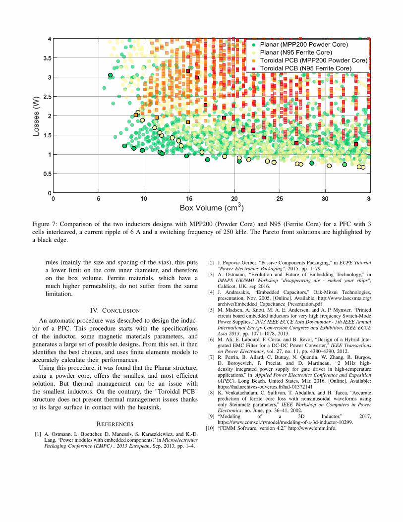
The results of the design procedure, for both designs andtwo magnetic materials are presented in Fig. 7. In each case,these results are represented as a cloud of points (one pointper inductor configuration). The best points (low volume,low losses) which offer a maximum temperature of less than100 C constitute the Pareto Front. The box dimensions oftwo examples are given in table III.
Inductor Design Planar (Green) Toroidal PCB (Orange)Magnetic Material MPP 200 MPP 200Power Loss (W) 1.21 2.02Box Volume (cm3) 8.61 9.10Box Dimensions (cm3) 3.3 x 2.9 x 0.9 5.33 x 5.33 x 0.32
Table III: Dimensions for two inductors on the Pareto front(Planar and Toroidal PCB) using MPP200.
From these results, the following conclusions can be drawn:• The planar structure tends to offer lower losses and lower
volume. This is because the maximum allowed thicknessfor the Toroidal PCB structure tends to results in flat coreswith a large diameter, imposing longer copper windingsand therefore higher copper losses.
• For the planar structure, many points were removed fromthe Pareto front, because of the high temperatures reachedin the inductor. On the contrary, for the Toroidal PCBstructure, the Pareto front follows exactly the bottomboundary of the cloud. This means that the thermalconsiderations are not a limiting factor for this structure(because of its efficient cooling, due to its large surface).
• With the powder core materials, only a handful of"Toroidal PCB" designs are possible: due to the intrinsiclow permeability of these materials, a relatively largenumber of turns is necessary. Because of the PCB design
0 5 10 15 20 25 30 350
0.5
1
1.5
2
2.5
3
3.5
4
0 5 10 15 20 25 30 35
0.5
1
1.5
2
2.5
3
3.5
4
00 5 10 15 20 25 30 35
0
0.5
1
1.5
2
2.5
3
3.5
4
Box Volume (cm3)
Loss
es (
W)
Planar (MPP200 Powder Core)Planar (N95 Ferrite Material)Toroidal PCB (MPP200 Powder Core)Toroidal PCB (N95 Ferrite Core)
Toroidal PCB (N95 Ferrite Core)
Figure 7: Comparison of the two inductors designs with MPP200 (Powder Core) and N95 (Ferrite Core) for a PFC with 3cells interleaved, a current ripple of 6 A and a switching frequency of 250 kHz. The Pareto front solutions are highlighted bya black edge.
rules (mainly the size and spacing of the vias), this putsa lower limit on the core inner diameter, and thereforeon the box volume. Ferrite materials, which have amuch higher permeability, do not suffer from the samelimitation.
IV. CONCLUSION
An automatic procedure was described to design the induc-tor of a PFC. This procedure starts with the specificationsof the inductor, some magnetic materials parameters, andgenerates a large set of possible designs. From this set, it thenidentifies the best choices, and uses finite elements models toaccurately calculate their performances.
Using this procedure, it was found that the Planar structure,using a powder core, offers the smallest and most efficientsolution. But thermal management can be an issue withthe smallest inductors. On the contrary, the "Toroidal PCB"structure does not present thermal management issues thanksto its large surface in contact with the heatsink.
REFERENCES
[1] A. Ostmann, L. Boettcher, D. Manessis, S. Karaszkiewicz, and K.-D.Lang, “Power modules with embedded components,” in MicroelectronicsPackaging Conference (EMPC) , 2013 European, Sep. 2013, pp. 1–4.
[2] J. Popovic-Gerber, “Passive Components Packaging,” in ECPE Tutorial"Power Electronics Packaging", 2015, pp. 1–79.
[3] A. Ostmann, “Evolution and Future of Embedding Technology,” inIMAPS UK/NMI Workshop "disappearing die - embed your chips",Caldicot, UK, sep 2016.
[4] J. Andresakis, “Embedded Capacitors,” Oak-Mitsui Technologies,presentation, Nov. 2005. [Online]. Available: http://www.laocsmta.org/archive/Embedded_Capacitance_Presentation.pdf
[5] M. Madsen, A. Knott, M. A. E. Andersen, and A. P. Mynster, “Printedcircuit board embedded inductors for very high frequency Switch-ModePower Supplies,” 2013 IEEE ECCE Asia Downunder - 5th IEEE AnnualInternational Energy Conversion Congress and Exhibition, IEEE ECCEAsia 2013, pp. 1071–1078, 2013.
[6] M. Ali, E. Labouré, F. Costa, and B. Revol, “Design of a Hybrid Inte-grated EMC Filter for a DC-DC Power Converter,” IEEE Transactionson Power Electronics, vol. 27, no. 11, pp. 4380–4390, 2012.
[7] R. Perrin, B. Allard, C. Buttay, N. Quentin, W. Zhang, R. Burgos,D. Boroyevich, P. Preciat, and D. Martineau, “2 MHz high-density integrated power supply for gate driver in high-temperatureapplications,” in Applied Power Electronics Conference and Exposition(APEC), Long Beach, United States, Mar. 2016. [Online]. Available:https://hal.archives-ouvertes.fr/hal-01372141
[8] K. Venkatachalam, C. Sullivan, T. Abdallah, and H. Tacca, “Accurateprediction of ferrite core loss with nonsinusoidal waveforms usingonly Steinmetz parameters,” IEEE Workshop on Computers in PowerElectronics, no. June, pp. 36–41, 2002.
[9] “Modeling of a 3D Inductor,” 2017,https://www.comsol.fr/model/modeling-of-a-3d-inductor-10299.
[10] “FEMM Software, version 4.2,” http://www.femm.info.