computational modeling of amorphous sio …
TRANSCRIPT

COMPUTATIONAL MODELING OF AMORPHOUS SiO2 NANOPARTICLES AND
THEIR ELECTRONIC STRUCTURE CALCULATION
A THESIS IN PHYSICS
Presented to the Faculty of the University of Missouri-Kansas City in partial fulfillment of
the requirements for the degree
MASTER IN SCIENCE
by CHANDRA DHAKAL
B.Sc., Tribhuvan University, Biratnagar, Nepal, 2003
M.Sc., Tribhuvan University, Kathmandu, Nepal, 2005
Kansas City, Missouri 2015

© 2015
CHANDRA DHAKAL
ALL RIGHTS RESERVED

iii
COMPUTATIONAL MODELING OF AMORPHOUS SiO2 NANOPARTICLES AND
THEIR ELECTRONIC STRUCTURE CALCULATION
Chandra Dhakal, Candidate for the Master in Science Degree
University of Missouri-Kansas City, 2015
ABSTRACT
The spherical amorphous silica (a-SiO2) nanoparticles (NPs) are constructed from a
previous continuous random network (CRN) model of a-SiO2 with the periodic boundary.
The models of radii 12 Å, 15 Å, 18 Å, 20 Å, 22 Å, 24 Å and 25 Å are built from the CRN
structure. Then, three types of models are constructed. Type I has the surface dangling bonds
not pacified. In type II models, the dangling bonds are pacified by hydrogen atoms. In type
III models, the dangling bonds are pacified by the OH groups. These large models are used to
perform the electronic structure calculation of NPs by using the orthogonalized linear
combination of atomic orbital (OLCAO) method. The results show some trends in band gap
variation for Type I models. The trends in band gap variation for other two types are less
clear.
A series of NP models with a spherical pore in the middle of a solid NP model are
constructed and studied. Spherical pores of radii of 6 Å, 8 Å, 10 Å, 12 Å, 14 Å, 16 Å and 18
Å are introduced within the spherical model of radius 20 Å. After OLCAO calculation, it is
found that the band gap values remain constant (5 eV) up to 21.6% porosity and then
decreases with increased in porosity. The relation with thickness of the porous NP shell and
iv
the surface to volume ratio (S/V) with the calculated band gap are studied in the same
manner and will be discussed.
Key words: Amorphous silica, Continuous random network, Nanoparticles, Porous model,
Band gap, Porosity
v
APPROVAL
The faculty listed below, appointed by the Dean of the College of Arts and Sciences,
have examined a dissertation titled “Computational Modelling of a-SiO2 Nanoparticles and
their Electronic Structure Calculation” presented by Chandra Dhakal, candidate for the
Master in Science degree, and certify that in their opinion, it is worthy of acceptance.
Supervisory Committee
Wai-Yim Ching, Ph.D., Committee Chair
Department of Physics and Astronomy
Da-Ming Zhu, Ph.D.
Department of Physics and Astronomy
Paul Rulis, Ph.D.
Department of Physics and Astronomy
vi
CONTENTS
Page
ABSTRACT ............................................................................................................................ iii
LIST OF ILLUSTRATION .................................................................................................. viii
LIST OF TABLES .................................................................................................................. ix
ACKNOWLEDGEMENTS ..................................................................................................... x
CHAPTER
1. INTRODUCTION ............................................................................................................. 1
1.1 Amorphous silica and nanoparticle .............................................................................. 1
1.2 Nanoporous particles ................................................................................................... 8
1.3 Nanoparticles model .................................................................................................... 9
1.4 Nanoporous model ..................................................................................................... 15
2. THEORETICAL BACKGROUND ................................................................................. 19
2.1 Density functional theory ........................................................................................... 19
2.2 Hohenberg kohn theorem ........................................................................................... 20
2.3 Local density approximation...................................................................................... 23
3. METHOD ........................................................................................................................ 26
3.1 Orthogonalized linear combination of atomic orbitals .............................................. 26
4. RESULTS AND DISCUSSIONS .................................................................................... 33
4.1 Results ........................................................................................................................ 33
4.1.1 Model I ........................................................................................................... 34
4.1.2 Model II ......................................................................................................... 37
4.1.3 Model III ........................................................................................................ 41

vii
4.1.4 Porous model ................................................................................................. 44
4.2 Discussion .................................................................................................................. 50
5. CONCLUSION AND FUTURE WORK ........................................................................ 53
APPENDIX
A. ABBREVIATIONS ................................................................................................... 55
BIBLIOGRAPHY .................................................................................................................. 57
VITA ...................................................................................................................................... 65

viii
LIST OF ILLUSTRATIONS
Figure Page
1.1 Continuous random network of a-SiO2 with periodic boundary condition ....................... 5
1.2 Enlarge model of Continuous random network of a-SiO2 with periodic boundary
condition ............................................................................................................................ 6
1.3 a-SiO2 nanoparticle of radius 12 Å .................................................................................. 12
1.4 a-SiO2 nanoparticle of radius 15 Å .................................................................................. 13
1.5 a-SiO2 nanoparticle of radius 18 Å .................................................................................. 13
1.6 a-SiO2 nanoparticle of radius 20 Å .................................................................................. 14
1.7 a-SiO2 nanoparticle of radius 22 Å .................................................................................. 14
1.8 a-SiO2 nanoparticle of radius 24 Å .................................................................................. 15
1.9 a-SiO2 nanoparticle of radius 25 Å .................................................................................. 15
1.10 a-SiO2 nanoporous model .............................................................................................. 18
4.1 PDOS plots of model I at less accurate potential ............................................................. 35
4.2 PDOS plots of model I at more accurate potential .......................................................... 36
4.3 PDOS plots of model II at less accurate potential ........................................................... 39
4.4 PDOS plots of model II at more accurate potential ......................................................... 40
4.5 PDOS plots of model III at less accurate potential .......................................................... 42
4.6 PDOS plots of model III at more accurate potential ........................................................ 43
4.7 PDOS plots of porous models at less accurate potential.................................................. 46
4.8 PDOS plots of porous models at more accurate potential ............................................... 48
4.9 Other relations with band-gap of porous model .............................................................. 49

ix
LIST OF TABLES
Table Page
1 Introduction of nanoparticle model in tabulated form ............................................... 10
2 Introduction of nanoporous model in tabulated form ................................................ 16

x
ACKNOWLEDGMENTS
I would like to express my sincere gratitude to my academic advisor Professor Wai-
Yim Ching for his guidance, support and advice in accomplishing my research thesis. I am
very fortunate to have him as my advisor.
I am grateful to Professor Da-Ming Zhu and Professor Paul Rulis for their
cooperation, encouragement and valuable suggestion for this research and kindly for serving
in my supervisory committee.
I would like to convey my sincere gratitude to Mr. Lokendra Poudel and Mr. Chamila
Dharmawardhana for their advice and assistance to my research work. I am grateful to all
friends (Electronic structure group and computational physics group) who directly or
indirectly helped me by offering their valuable advice and comments towards improving my
research work.

xi
Dedicated to My Family
1
CHAPTER 1
INTRODUCTION
1.1 Amorphous SiO2 and Nanoparticle
Computational Physics is one of the most essential researches in the field of material
sciences, which is not possible without computers. It is the first application of modern
computers from the very beginning. Sometimes, it is considered as an intermediate between
theoretical and experimental Physics. There are different mathematical complex formulas
and the approximations in many body problems where the computational method can work
efficiently to solve the problem. The problem in the theoretical physics can be solved
computationally, which may not possible by analytical calculation. It helps to study and
implement the idea of numerical analysis to solve the problem. In order to unravel any
questions in Physics, the notions of theoretical Physics are the basics tools. The
computational Physics is also essential to construct the model of material such as
nanoparticles (NPs). It is easier to select the small number of atoms while we construct the
model, but difficult to choose the atoms if structures contain several hundred/thousands of
atoms. Therefore, the computers are the required tool for such complex task. The use of
quantum mechanics is also important in theoretical research to determine the electronic
structure calculation. It is helpful to give information about the properties of matter, hence
suitable to describe the electronic structure of NPs.
78% of the earth’s crust consists of Silicon and Oxygen. Silica (SiO2) can be found in
both amorphous and crystalline form. Crystalline silica exists in multiple forms such as -
quartz, -quartz, trydimite and cristobalite. Amorphous silica is divided into natural
2
specimen such as diatomaceous earth, opal, silica glass and artificial products. Amorphous
silica also found in living organisms such as sponges, algae. Silica is one of the most
complex and ubiquitous materials on the earth [1, 2] . With the exception of stishovite and
fibrous silica, the Silicon (Si) atoms in silica show tetrahedral coordination (SiO4) with four
Oxygen atoms surrounding a central Si atom. The amorphous silica, (a- SiO2), also possesses
SiO4 units, i.e. exhibits only short-range ordering of their atoms. Small portion of crystalline
silica is used to observe the whole crystalline form with a non-repeating pattern. It cannot be
done in amorphous silica. Some short range orderliness may exist, but no definite order
extends over a whole range of the a-SiO2 form. Generally, the crystalline silica has ordered
structure and amorphous silica has disordered structure. There are significant differences
between them for the amount and rate of contaminants absorption and desorption. Therefore,
surface ordering can decrease hydrocarbons adsorption, and surface contamination can be
removed more easily with chemical cleaning and lower temperatures [3]. The type, depth
distribution, and density of defects depend on the growth and post-growth processes
experienced by the material. The expectation of the density of unsaturated bonds at the very
surface, Oxygen vacancies in the near selvedge or even across the whole layer as well as the
mismatching (geometrical) defects is related to the amorphous domains size and distribution.
The a-SiO2 is one of the best studied amorphous materials that have broad industrial
applications. There is great literature on such topics.
Nanotechnology is the manipulation of the dimension of material into their atomic,
molecular, and supramolecular scale with their distinct properties. It is going to be a rapidly
emerging artificial stuff in material science. The Mihail Roco of the U. S. national
nanotechnology institute shows the four generations of nanotechnology. The current phase is

3
that of passive nanostructures, which are made to perform one task. The next phase will
introduce active nanostructures for multipurpose use such as actuators, drug delivery, and
sensors. The third generation is projected around 2010 and will feature the nano-systems with
thousands of interacting components. After that, the first integrated nano-system, acting
similar to the animal cells with hierarchical systems within the systems, are expected to
evolve.
Nanoparticles (NPs) are the small objects of size between 1nm and 100nm [4] that act as
a complete unit to study its physical properties and transport phenomena, however, there is
no standard size that exists in this scientific field. The materials at this scale basically show
nanostructure dependent unique physical properties (optical, electrical and magnetic) and
high chemical reactivity. It is well-known that many physicochemical properties of NPs
could affect their biological activity. The NPs size is one of the most important factors in
determining the particular biological behaviors of nanomaterials. The NPs possess specific
large surface area because of their extreme small size and the number of surface atoms
increasing exponentially. It allows a greater proportion of its atoms or molecules to be
displayed on the surface rather than the interior of the material. Therefore, the NPs exhibit
higher chemical and biological reactivity than the fine particles [5]. The NPs are both natural
and artificial. The man made NPs are i) Fullerenes and Carbon Nanotubes, ii) Metals iii)
Ceramics iv) Quantum dots and v) Polymeric [6]. The unique properties of NPs are often
caused their extremely high surface area to volume ratio [7]. The NPs modelling and their
simulation are fascinating due to their size and composition. Many researchers introduced the
NPs differently. The most recent definition is based on the surface area, where they should
have specific area greater than 60 m2/cm3 [8]. The increase in surface area determines the

4
potential number of reactive groups on their surface. This measurement reflects the crucial
importance in different properties of NPs especially in commercial and medical applications
[9].
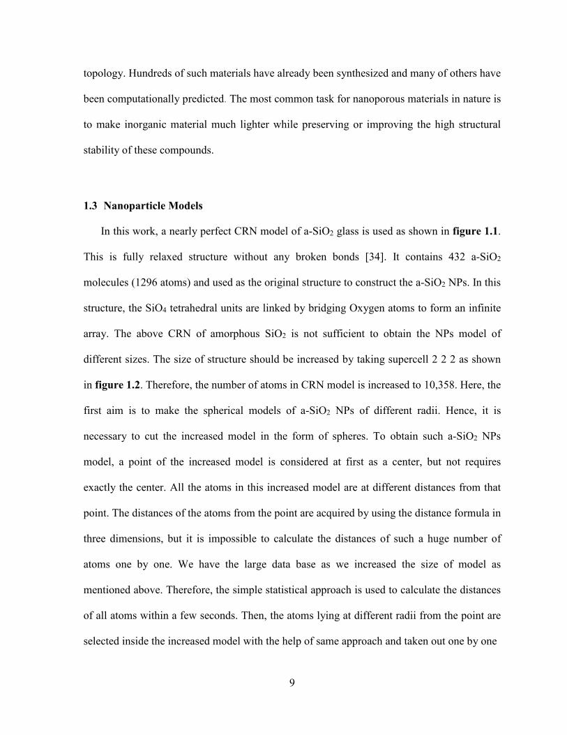
The a-SiO2 is an inorganic material in simple binary model system. Its initial model
contains three dimensional continuous random networks (CRN) of 432 a-SiO2 molecules
[10] (1296 atoms) as shown in figure 1.1. This model has periodic boundary without any
broken bonds and hence the structure is unique. In general, each Silicon atom is bonded to
four Oxygen atoms and each Oxygen atoms are connected to again two Si atoms. Then the
Silicon and Oxygen are fully coordinated and hence there are no dangling bonds inside the
CRN model. In particular, the CRN model does not allow the defects. Hence, there is the
chance of decreasing the strain in amorphous network. Some works were done on that model
by former co-worker in UMKC [11, 12, 13, 14]. This is the basic structure of a-SiO2 for the
further research on it, such as the a-SiO2 NPs modelling. The CRN of a-SiO2 model doesn’t
have sufficient numbers of atoms as we need to build NPs model. In order to get the different
sizes of it, the size of supercell of CRN model is increased to 2⨯2⨯2 from 1⨯1⨯1 as shown
in figure 1.2. Eventually, the total number of atoms on a-SiO2 models became 10,358. To get
different sizes of a-SiO2 NPs, the data of enlarged CRN model are extracted by choosing a
point inside the structure (figure 2) and distances of each and every atom are obtained from
that point by using simple statistical technique. Then, the spherical structures of nanoparticles
of a-SiO2 of different radii are selected from the same data analysis.
The a-SiO2 NPs have been extremely important in material science and nanophysics
due to their enormous technological importance. Their modelling and simulation are
interesting because of their size and structure. The a-SiO2 NPs have attracted the various

5
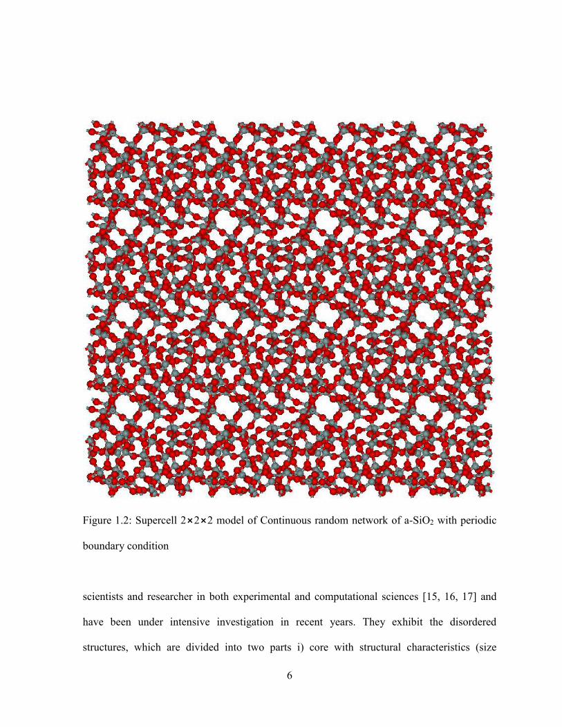
Figure 1.1: Continuous random network of a-SiO2 with periodic boundary condition
6
Figure 1.2: Supercell 2⨯2⨯2 model of Continuous random network of a-SiO2 with periodic
boundary condition
scientists and researcher in both experimental and computational sciences [15, 16, 17] and
have been under intensive investigation in recent years. They exhibit the disordered
structures, which are divided into two parts i) core with structural characteristics (size
7
independent) close to that of the corresponding amorphous bulk counterparts [18] and ii)
surface showing the defects such as the pores because of the existing structure [19], higher
concentration of coordinately unsaturated sites and dangling bonds. The interior of the NPs
structure is mentioned in (i), but the surface atoms may not be fully coordinated with each
other. Due to less coordination, the atoms may separate a little to form the vacancies
including unsaturated sites. There is no any rule to determine the surface shell of a-SiO2 NPs.
It is easier to distinguish the shell from the structural point of view of the NPs. The shell can
be assumed that the atoms lying on the surface have no complete coordination to all atomic
pairs. Due to the defects, a-SiO2 NPs have more innovative significance with well-defined
applications such as catalysis [20], chemical reaction [21] and micro-electronic fabrication
[22]. Because of emerging commercialization in the realm of nanotechnology, they are used
in electronic and optoelectronic devices [23, 24], as additives to cosmetics [25], printers [26],
varnishes [27] and food [28]. Moreover, a-SiO2 NPs have been used for the host of
biomedical and biotechnological application such as cancer therapy [29], DNA transfection,
enzyme mobilization [30], gene delivery, drug release control, photoluminescence [31] and
as carriers for indomethacin in solid state dispersion. Also, the common use of silica NPs
generates various sources for potentials in human exposure. It is possible for a-SiO2 NPs to
enter inside the human body through inhalation, ingestion, dermal penetration and injection
[8]. The meticulous study of a-SiO2 NPs surfaces is crucial for addressing the more practical
applications of these ubiquitous materials. Also, the structure and properties of a-SiO2 NPs
are different from their corresponding amorphous bulk counterparts. There are number of
methods for synthesis and characterization of amorphous NPs. Also, the diffraction technique
is used to get the structural characteristics of a-SiO2 NPs, however, the computer simulation

8
is required to get the detailed information of microstructure of the amorphous NPs at atomic
level. Therefore, a-SiO2 NPs become the interesting research material for computer
simulation because of their smaller size [32]. The amorphous a-SiO2 NPs have the other
advanced potential applications in different areas of technology [33].
1.2 Nanoporous Particle
The NPs have holes of varying in size are called nanoporous particle. Usually, the
diameter of holes are less than 100 nm. The porous material are scientifically important
because of the presence of voids or space of dimension at atomic, molecular and nanometer
scales. The most interesting thing is that there is nothing inside the hole. If some interesting
molecules are put inside the pore, their interaction with the NPs surface is detected. The
nanoporous materials are divided into three types by International Union of Pure and Applied
Chemistry (IUPAC). (i) The pore of diameter less than 2 nm are micropores. (ii) Those of
diameter between 2 – 50 nm are termed as mesopores and (iii) the pore diameter greater than
50 nm are macropores. They are found in both biological systems and in natural minerals.
Nanoporous materials in nature are organic-inorganic hybrids. Naturally occurring materials
exhibit synergistic properties. In the past two decades, the field of nanoporous materials has
undergone significant developments. There has been increasing interest and research effort in
the synthesis, characterization, functionalization and designing of nanoporous material. The
main challenges in research include the fundamental understanding of structure-property
relations and tailor-design of nanostructures for specific properties and applications. As these
materials possess high specific surface areas, well-defined pore sizes, and functional sites,
they show a great diversity of applications in many industrial fields. The large number of
unique nanoporous material can be synthesized, varying in chemical composition and
9
topology. Hundreds of such materials have already been synthesized and many of others have
been computationally predicted. The most common task for nanoporous materials in nature is
to make inorganic material much lighter while preserving or improving the high structural
stability of these compounds.
1.3 Nanoparticle Models
In this work, a nearly perfect CRN model of a-SiO2 glass is used as shown in figure 1.1.
This is fully relaxed structure without any broken bonds [34]. It contains 432 a-SiO2
molecules (1296 atoms) and used as the original structure to construct the a-SiO2 NPs. In this
structure, the SiO4 tetrahedral units are linked by bridging Oxygen atoms to form an infinite
array. The above CRN of amorphous SiO2 is not sufficient to obtain the NPs model of
different sizes. The size of structure should be increased by taking supercell 2 2 2 as shown
in figure 1.2. Therefore, the number of atoms in CRN model is increased to 10,358. Here, the
first aim is to make the spherical models of a-SiO2 NPs of different radii. Hence, it is
necessary to cut the increased model in the form of spheres. To obtain such a-SiO2 NPs
model, a point of the increased model is considered at first as a center, but not requires
exactly the center. All the atoms in this increased model are at different distances from that
point. The distances of the atoms from the point are acquired by using the distance formula in
three dimensions, but it is impossible to calculate the distances of such a huge number of
atoms one by one. We have the large data base as we increased the size of model as
mentioned above. Therefore, the simple statistical approach is used to calculate the distances
of all atoms within a few seconds. Then, the atoms lying at different radii from the point are
selected inside the increased model with the help of same approach and taken out one by one

10
Table 1: Introduction of nanoparticle model in tabulated form
in the form of spheres of respective surface areas are shown in above table. Therefore, the
spherical models of a-SiO2 NPs of radii 12 Å, 15 Å, 18 Å, 20 Å, 22 Å, 24 Å and 25 Å are
built as the initial models for our calculation. These models contain the broken bonds on the
surface, either on Silicon or Oxygen or on both, called dangling bonds. As one would
expect, a more disordered surface has more surface defects to interact with contaminants
while an ordered surface with fewer dangling bonds can be more stable, adsorb fewer
hydrocarbons, and desorb them more easily (need to locate position). The dangling bonds on
the surface are saturated by H-atoms. In this process, the silanol (SiOH) and silane like
compounds (SiH, SiH2) are formed on the surface of the a-SiO2 NPs. The silane is the silicon
analogue of methane. Hydrogen in silane is more electronegative than Silicon. So, Hydrogen
has partial negative charge and Silicon has positive charge. It is the gas at normal
temperature and easily combustible in air without external ignition. Silane and silane like
Radius(Å) No. of Si No. of O No. of H Total Area(Å2) a=b=c Volume(Å3)
12 163 327 120 610 1808.64 45 91125
15 308 615 196 1119 2826 50 125000
18 532 1065 278 1875 4069.44 55 166375
20 735 1470 356 2561 5024 62 238328
22 978 1956 410 3344 6079.04 65 274625
24 1272 2535 509 4315 7234.56 65 274625
25 1443 2886 544 4873 7850 70 343000

11
compounds on the surface of NPs are used as coupling agents to adhere fibers to certain the
polymer matrix. They are also applied to couple a bio-inert layer on a titanium implant, water
repellents, masonry protection, control of graffiti [35], manufacturing semiconductor and
sealants. The Si-H bonds are used as reducing agents in organic and organometallic
chemistry [36]. The silanol (OH) group on the surface of a-SiO2 NPs is bounded via the
valence bond with Si atoms on the silica surface. The surface of a-SiO2 is oxide absorbent
and depends on the presence of silanol groups. The surface becomes hydrophilic in presence
of sufficient concentration of these silanols. The OH groups act as the centers of molecular
adsorption by interacting with absorbates capable of forming the Hydrogen bonds with the
OH groups. The adsorption property of NPs surfaces decreases by removing the hydroxyl
groups. Hence, their hydrophobic property increases. These models explained are the
preliminary one. In our improved models, there is the pure a-SiO2 NPs with a fully Oxygen
terminated surface. It means the bonds are broken only on the surface of Oxygen atoms, not
Silicon. Again, the dangling bonds created by Oxygen atoms are saturated by H-atoms and
silanols are formed on the a-SiO2 NPs surface.
To make the a-SiO2 NPs model of radius 12 Å (1.2 nm), a point is taken inside the
enlarged model as mentioned above. Then, the atoms lying at the distance of 12 Å from that
point are selected and taken out. It looks like as we cut the sphere of radius 12 Å from the
enlarged model. During the selection of atoms, the bonds are broken either on Oxygen or
Silicon or both, which takes place only on the surface. These broken bonds are called
dangling bonds. There is no broken bond inside the model. The model consists of outer shell
and inner core. The surface has some defects and dangling bonds as mentioned above. The
models with dangling bonds are unsaturated that can add more other atoms for their

12
(a) (b) (c)
Figure 1.3: a-SiO2 nanoparticle of radius 12 Å
neutrality. Then, H – atoms are added on the unsaturated model so that the dangling bonds
are occupied by these atoms as shown in figure 1.3 (a). Also, before adding H-atoms, each
Silicon atoms on the surface may not be connected with four Oxygen atoms. Therefore, the
extra O-atoms have to be added to Silicon to make the Oxygen coordinated as shown in
figure 1.3(b). The Oxygen atoms on the surface of model have the dangling bonds. This
model is also the unsaturated one. Again, H-atoms are added on models of figure 1.3 (b) in
such a way that these atoms are bonded with oxygen atoms lying on the surface (shell) of
model. Therefore, the H-atoms are connected with O- atoms not the Silicon as shown in
figure 1.3(c).
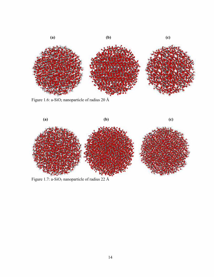
Similarly, the atoms lying within the distances of 15 Å, 18 Å, 20 Å, 22 Å, 24 Å and
25 Å are carefully selected and taken out in the form of sphere. The atoms lying inside the
spherical models are all bonded, but there are some danggling bonds on the surface of
spherical a-SiO2 NPs. These bonds are occupied after the addition of H-atoms as shown in
figure 1.3(a), 1.4(a), 1.5(a), 1.6(a) and 1.7(a). The Oxygen atoms are added on the Silicon
atoms on the surface of each model, which have the danglling bonds before. Hence, each

13
(a) (b) (c)
Figure 1.4: a-SiO2 nanoparticle of radius 15 Å
Silicon atom on the surface are connected to four Oxygen atoms, not any H-atoms as shown
in figure 1.4(b), 1.5(b), 1.6(b) and 1.7(b). The models contain dangling bonds on the
Oxygen atoms that lie on the surface. Then, the H- atoms are added on this model and the
dangling bonds are saturated by H-atoms. Then, the model is fully saturated as shown in
figure 1.4(c), 1.5(c), 1.6(c) and 1.7(c). During the saturation of structure, SiOH and SiH
compounds are formed on the a-SiO2 NPs surface as in spherical models of varying radii.
(a) (b) (c)
Figure 1.5: a-SiO2 nanoparticle of radius 18 Å
14
(a) (b) (c)
Figure 1.6: a-SiO2 nanoparticle of radius 20 Å
(a) (b) (c)
Figure 1.7: a-SiO2 nanoparticle of radius 22 Å

15
Figure 1.8: a-SiO2 nanoparticle of radius 24 Å
Figure 1.9: a-SiO2 nanoparticle of radius 25 Å
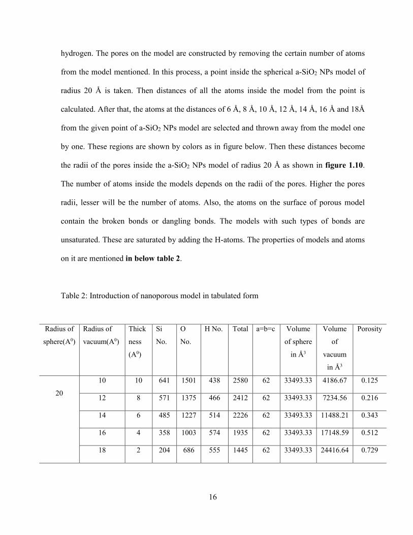
1.4 Nanoporous Model
The pores found on the a-SiO2 NPs model are the smaller holes of varying diameter.
The spherical a-SiO2 NPs model of radius 20 Å is taken as an initial structure without
16
hydrogen. The pores on the model are constructed by removing the certain number of atoms
from the model mentioned. In this process, a point inside the spherical a-SiO2 NPs model of
radius 20 Å is taken. Then distances of all the atoms inside the model from the point is
calculated. After that, the atoms at the distances of 6 Å, 8 Å, 10 Å, 12 Å, 14 Å, 16 Å and 18Å
from the given point of a-SiO2 NPs model are selected and thrown away from the model one
by one. These regions are shown by colors as in figure below. Then these distances become
the radii of the pores inside the a-SiO2 NPs model of radius 20 Å as shown in figure 1.10.
The number of atoms inside the models depends on the radii of the pores. Higher the pores
radii, lesser will be the number of atoms. Also, the atoms on the surface of porous model
contain the broken bonds or dangling bonds. The models with such types of bonds are
unsaturated. These are saturated by adding the H-atoms. The properties of models and atoms
on it are mentioned in below table 2.
Table 2: Introduction of nanoporous model in tabulated form
Radius of
sphere(A0)
Radius of
vacuum(A0)
Thick
ness
(A0)
Si
No.
O
No.
H No. Total a=b=c Volume
of sphere
in Å3
Volume
of
vacuum
in Å3
Porosity
20
10 10 641 1501 438 2580 62 33493.33 4186.67 0.125
12 8 571 1375 466 2412 62 33493.33 7234.56 0.216
14 6 485 1227 514 2226 62 33493.33 11488.21 0.343
16 4 358 1003 574 1935 62 33493.33 17148.59 0.512
18 2 204 686 555 1445 62 33493.33 24416.64 0.729

17
(a) (b) (c)
rp = 6A0 rp = 8A0 rp = 10A0
(d) (e) (f)
rp = 12A0 rp = 14A0 rp = 16A0
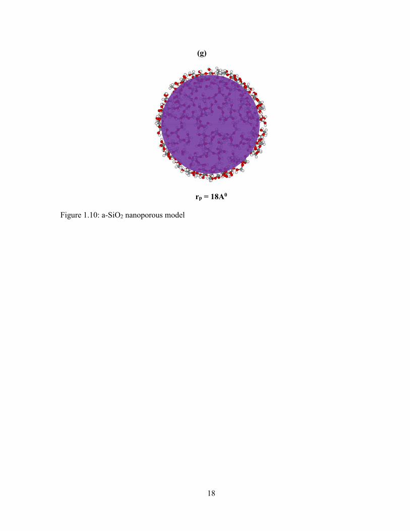
18
(g)
rp = 18A0
Figure 1.10: a-SiO2 nanoporous model

19
CHAPTER 2
THEORETICAL BACKGROUND
The Orthogonalized Linear Combination of Atomic Orbitals (OLCAO) [37] is mainly
based on the density functional theory (DFT). DFT is one of the approaches of first principle
calculation, which is relatively new and based upon the quantum mechanical theory from the
1920’s. Here, many electron systems are described in terms of one electron wave functions.
2.1 Density Functional Theory
DFT is used to investigate the electronic structure (principally the ground state) of
many body systems, particularly in atoms, molecules and condensed phases. The functional
is the electron density which is a function of space and time. DFT comes from the use of
functional (functions of another function) of the electron density to reduce a many-electron to
a single-particle problem. The electron density is used in DFT as the fundamental property
unlike Hartree-Fock (HF) theory [38, 39], which deals directly with the many-body wave
function. Using the electron density significantly speeds up the calculation, whereas the
many-body electronic wave function is a function of 3N variables (the coordinates of all N
atoms in the system). It was Hohenberg and Kohn who stated a theorem which tells us that
the electron density is very useful. By focusing on the electron density, it is possible to derive
an effective one-electron-type Schrödinger equation. This is not enough from the structural
view of many solids. Therefore, one electron system is converted into many electrons and the
concept of linear combination of atomic orbital (LCAO) is useful to solve the Schrödinger
equation because it tries to define the structure of solids in terms of its constituents [40].

20
Time-dependent density-functional theory (TDDFT) is an extension of the static ground
state DFT [41]. Despite the failure of DFT, its use continues to increase from the
approximations made for the exchange – correlation contributions, because of its wide
applicability and its favorable scaling with the number of atoms. In the past, the TDDFT [42,
43, 44, 45] has used to do the calculation of electronic excitations of both finite and infinite
system. Currently, it is also used to describe excited state properties of molecules with finite
systems with large numbers of atoms. A wide variety of spectroscopic techniques is being
used to characterize the electronic structure and dynamics of these systems by probing their
excited spectra. The performance of any nano-electronic device, such as a molecular junction
is dominated by its electronic excitations. Here, below is the summary of foundation of DFT
and its connection with the excited state properties and many body perturbation theories.
2.2 Hohenberg-Kohn Theorem
The DFT is based on the H-K theorems [46]. In first theorem, for a system of N
interacting (spinless) electrons, there exists an external potential V (r) (usually the Coulomb
potential of the nuclei). There is only one charge density n(r) for non-degenerate ground
state system that corresponds to a given V (r) without existence of an external magnetic field.
After this, the improvements have been made to accommodate the entire system [47]. Here,
the electron density represents the total energy and the wave function of system. The second
H-K theorem is based on the ground state energy as a minimum versus particle density
variation under normalization condition.
For many-electron system, the Hamiltonian, H with ground state wave function Ψ is
given by

21
H T U V= + + (2.1)
where T is the kinetic energy, U the electron-electron interaction, V the external potential.
The charge density n(r) is defined as
∫= nn drdrrrrrNrn ...............,,()( 2
2
21ψ (2.2)
Consider the different Hamiltonian,
'' VUTH ++= (2.3)
(V and V’ do not differ simply by a constant: V – V’ = const.), with ground state wave
function Ψ’. Suppose ground state charge densities are same. Then,
)()( 'VnVn = (2.4)
Therefore, the following inequality holds
ψψψψψψ VVHHHE −+=<= ''''''' (2.5)
Then, we have
∫ −+< drrnrVrVEE )())]()([( '' (2.6)
Here, Ψ and Ψ’ are different, being the eigenstates of different Hamiltonians. Two different
potentials can’t have same charge density because we obtained absurd result by reversing the
primed and unprimed quantities. From the consequence of the first Hohenberg and Kohn
theorem, the ground state energy, , is also uniquely determined by the ground-state charge
density. In mathematical terms, is a functional [n(r)] of n(r). We can write
∫+=++=++= drrVrnrnFVUTVUTrnE )()()]([)]([ ψψψψψψ (2.7)
where F[n(r)] is unknown but it is the functional of the electron density and [n(r)] is a
universal functional of the charge density n(r) (and not of V (r)). In this way, DFT exactly
reduces the N-body problem to the determination of a 3-dimensional function n(r) which

22
minimizes a functional [n(r)]. In addition, the TDDFT has been used to calculate the excited
states. The energy functional [n(r)] in Kohn and Sham [48] approach of electron effective
potential Veff(r) is given by
)]([)]([)]([)]([)]([ rnErnUrnErnErnE XCieeek +++= −− (2.8)
where [n(r)] is kinetic energy of the electrons, e-e [n(r)] is the electron-electron energy,
e-i[n(r)] is the electron-ion interaction potential and XC[n(r)] is the exchange-correlation
energy resulting from the Pauli exclusion principle and other factors which are not exactly
known. In practice, the kinetic energy and exchange-correlation give the moderate
quantitative agreement with the experimental data [49]. Here,
∑∫=
∇−=N
i
iik drrrrnE1
2* )()(2
1)]([ ψψ (2.9)
∫∫ −=−
'
'
' )()(
2
1)]([ drdr
rr
rnrnrnE ee
(2.10)
∫=− )()()]([ rdrnVrnU extie (2.11)
The second HK theorem tells about the minimization of the total energy through the electron
density. For a fixed number of electrons, N, and the given external potential, the minimizing
[n(r)]- N, is a method of Lagrange multipliers. Then
[ ] 0)()()]([)(
=− ∫ rdrnrnErn
µδ
δ (2.12)
)(
)]([
rn
rnE
δδµ =⇒ (2.13)
where is the Lagrange multiplier with constraint ∫ = Ndrrn )(
From equations (2.8) and (2.13), we get

23
µδ
δδ
δδ
δδ
δ =
+++ −−
)(
)]([
)(
)]([
)(
)]([
)(
)]([
rn
rnE
rn
rnU
rn
rnE
rn
rnE XCieeek (2.14)
By using effective potential eff as
µδ
δ =+ )()(
)]([rV
rn
rnEeff
k (2.15)
where,
∫ +−
+= )()()(
)()( '
'
'
rVrdrr
rnrVrV XCexteff
(2.16)
and
)(
)]([)(
rn
rnErV XC
XC δδ= (2.17)
Also, the one-electron Schrödinger’s equation is given by
iiieff rrV ψεψ =
+∇− )()(2
1 2 (2.18)
From the solutions of above equation, the ground state energy, E0, and the ground state
density 0(r) are determined. The KS approach is an exact in theoretical calculation but the
exchange-correlation functional, XC[n(r)], is unknown in reality.
2.3 Local Density Approximation
Both KS and HF equations are derived from the variational principle and are also self
–consistent equations for one electron wave function. The exchange term in HF equation
appear in the place of the exchange correlation potential of KS equation.
∑∫ =−
−
++∇−
||,
''
'
'*22
2
)()()()(
)()()(2 j
iii
jj
iH rdrrrr
rrerrVrV
m
h ψεψψψ
ψ (2.19)

24
where sum over j extends only to the states with parallel spin. Traditionally, correlation
energy is the difference between the HF and the real energy. The exchange term in HF
equation is the non-local operator – one acting on function as
∫= '' )(),()( drrrrVrV φφ (2.20)
and is quite difficult to compute.
Then,
)()())(( rrVrV x φφ = (2.21)
Also,
3/122
)](3[2
3)( rn
erVx π
π−= (2.22)
Within this approximation, the only difference between KS and HF equation is the form of
exchange correlation. As early as 1965, Kohn and Sham introduced the LDA. They
approximated exchange correlation energy with the function of local density n(r). Then, the
expression for exchange correlation energy functional is given by
∫= drrnrnrnE xcxc )()]([)]([ ε ;
)(])(
)([)]([)(
rnnxc
xcxcxc
dn
ndnnrn
rn
E=+=≡ εεµ
δδ
(2.23)
In this approximation, (n(r)) has same dependence upon the density as for the homogeneous
electron gas. The Latter is unknown except for HF level. The xc is the exchange-correlation
energy of an electron in the homogeneous electron gas of density n(r). The LDA can describe
the various ground state properties and overestimates the exchange part, but underestimates
its correlation resulting from the unexpected accuracy of Exc. The results obtained from the
LDA approximations are partially addressed the systematic error calculation [50]. Hence, it is

25
one of the most famous topics in solid state physics. It has also some limitations and different
methods are subjected for its improvement. In LDA, we generally take the local electron
density at some specific point, say r. The LDA avoids the variable electron density in real
system. Therefore, it is cleared that one can consider the rate of spatial variation of electron
density in exchange-correlation energy functional Exc. Also, highly accurate results from
Quantum Monte-Carlo techniques were found by Ceperley and Alder [51, 52] and
parameterized by Perdew and Zunger [53, 54] with a simple analytical form:
)3334.00529.11(
2846.09164.0)(
sss
xcrrr
n++
−−=ε for rs≥1
= 0960.0023.0ln0622.0ln0040.09164.0 −−++− ssss
s
rrrrr
for rs≤1 (2.24)
Here, rs is the Bohr radius and xc is in Ry. The first term is the HF exchange contribution
and the remaining terms is exchange correlation energy. Other forms of xc can also be found
in other forms of literature. All forms yield very similar results in condensed matter
calculations, which are not surprising, since all parameterizations are very similar in the
range of rs applicable for solid-state phenomena.
26
CHAPTER 3
METHODS
3.1 Orthogonalized Linear Combination of Atomic Orbitals (OLCAO)
The OLCAO package is an extension and the numerous additional modifications of
LCAO method. It is developed entirely at UMKC Electronic Structure Group (ESG) and
Computational Physics Group (CPG). It is an important and efficient for electronic properties
calculations of large complex system, both crystalline and non-crystalline substances [55, 56,
57, 58]. The OLCAO is based on the DFT of all electrons method using atomic orbitals for
the expansion of the bloch wave function. This method is appropriate for complex material
systems containing different types of elements with large number of atoms and materials
with low or no symmetry and so on. From the experience, it is possible to do fully self-
consistence calculation in amorphous structure and materials with defects and
microstructures. The details of the OLCAO method are mentioned in many past publications
especially in Ching (1990) [37] and in Ching and Rulis [59].
There were different methods to solve the Schrödinger’s equation for many electron
systems but the base of the OLCAO method can be seen back to the early days. The atomic
orbitals are very good to describe the atomic electronic configurations, and then it was
obvious procedure to use LCAO to construct the wave function for many electron systems.
The orthogonalized plane wave (OPW) method is developed by Conyers Herring [60] and it
is considered to be the first capable method of band structure calculation. The idea of OPW
method was used to improve LCAO which finally develop to modern OLCAO. It is very

27
useful in the electronic structure calculation and spectroscopic properties of solids. It is
mainly applied to large and complex systems.
In basis expansion, the radial part of atomic orbitals is expanded in the form of Gaussian
type of orbitals (GTO). The OLCAO package is strongly treated as band structure method
and it will succeed to maintain the electronic structure in terms of wave vector . The
expansion of solid state wave function Ψnk(r) in OLCAO method is given by in terms of
bloch sums biϒ(,r) as shown in following equation
Ψ = ∑ ()(, r), (3.1)
where represents nonequivalent atoms in the cell and is the quantum numbers , ! and .
The n marks the band index and is the wave vector. In the expression, the orbital quantum
number contains the principle quantum number, angular momentum quantum number and
spin quantum number.
The bloch sum bi (k, r) in above equation is expressed as linear combination of atom
centered atomic orbitals Ui(r) and given by
= "√$ ∑ %.'((r − t+ − R-)- (3.2)
where t is the position of the th atom in the cell and Rv represents the reciprocal lattice cell.
The atomic orbitals (i(r-t-RV) consist of both radial and angular parts. The radial parts are
expressed as the linear combination of GTO and spherical harmonics Y(θ,Ø) are used to
expand the angular parts. So, the equations are easier and faster to solve.
((.) = /∑ 0.1"%2134'56$0 789:(;, (3.3)
The first term of equation (3.3) is the radial part and is the linear combination of GTO and
second part is the angular part called spherical harmonics. The decaying constant, αj ranging
from αmin to αmax (0.15 to 107) and N has the common value ranging from 16 to 26. The atom
28
having the same wave function has the same set of exponentials (αj) and hence lowers the
computational cost for atoms with large number of orbitals. After the determination of
exponential set [j], the expansion coefficient Cj can be calculated by either the
normalization of eigen-vector coefficient of a single atom problem within the same DFT or
the linear fitting to atomic function in HF method. In the former method, eigen value
problem of an atom is solved self-consistently by using the Gaussian function. The ab initio
atomic calculation [61, 62] is also helpful to obtain the Cj. We need to know the basis
function of specific element and is already fixed in OLCAO method. Therefore, the
calculation of structure containing large number of atoms becomes efficient because it
reduces the number integrals to be evaluated during the process. Also, (i(r) contains the core
orbitals, the occupied valence orbitals and the other additional empty orbitals. Usually, the
minimal basis (MB) is sufficient for the calculation of amorphous structure with large
number of atoms which consists of core orbitals and the occupied or unoccupied orbitals in
the valence shell of the atom. They are used for the calculation of effective charge (Q*) and
bond order (BO) by using Mulliken scheme, but we didn’t do this part in our calculation. In
this method, the effective charge of an atoms and bond order measure the relative strength of
bond between two atoms. Also, the full basis (FB) is much more sufficient for the precise
results. FB has one more unoccupied orbital and is applied to the smaller system in general. It
is used for band structure and density of states (DOS) calculations. The calculations are
significant in presence of more unoccupied orbitals in the basis set. Hence, an additional shell
of the excited atomic basis is added to FB to obtain the extended basis (EB) in spectral
calculations, where unoccupied states at high energy are taken into account. Therefore, the
orthogonalisation of orbitals and the use of basis sets make the OLCAO package very

29
efficient and versatile for electronic and spectroscopic calculations. There are many choices
to select the atomic basis set in order to solve the problem with great accuracy within the
reasonable time interval.
In OLCAO method, the charge density (r) and the one-electron potential Vcry(r) are
also called the atom centered Gaussian function. Therefore, the charge density is
<(.) = ∑ ∑ =0%1>4'5(r − t?)0@"A (3.4)
where B(r) is total charge density at one point due to all atoms in the system. It is significant
and closes to true charge density.
CDE9(r) = ∑ / FG(') %1H'5 − ∑ I0%1>4'5$0@" 7 (r − t+) (3.5)
KL(.) = ∑ ∑ M0%1>4'5(r − t+)$0@" (3.6)
<(.) = ∑ 2L(.) + K(.)6(r − t+) (3.7)
where OB is the total potential at one point because of the all atoms in the system. OP is the
coulomb potential and Ox is the exchange-correlation potential. The coefficients βj are
predefined in database like αj for each atom and the βj values ranging from minimum to
maximum and numbers are arranged in geometric series between them. The term, Q is the
mass number of the atom at the site. All these terms depend on Z and on system used. The
coefficients Bj, Dj and Fj are updated at each self-consistent calculation until the difference of
energy eigen values between the two successive steps drops down to the specified minimum
value, 10-4 /10-5 eV. This convergence is important and easily obtained for non-conducting
system and their band gap is used to differentiate the occupied and unoccupied states. Since
the centered potential function is transferrable, the self-consistent potential obtained from
simple calculations can be used to calculate the properties of complex systems.

30
In OLCAO method, the one of important properties is core-orthogonalisation, where
the core orbitals are removed from the following secular equations
RS,0T(k) − V,0T(k)(k)R = 0 (3.8)
where, Hiγ, jδ (k) and Siγ, jδ (k) are Hamiltonian and overlap matrix respectively and the
overlap matrix is given by
V,0T(k) = X(k)R0T(k)Y (3.9)
Suppose the bloch sum with core orbitals, bcjβ(k,r) and the valence orbitals, bZ α(k,r). Hence,
the orthogonalized valence bloch sum bZ’ α (k,r) is given by
3[\(k, r) = 3[ + ∑ 030, 3C (k, r) (3.10)
where
03 = −X0C (k, r)R3[ (k, r)Y
and
03∗ = −X3[ (k, r)R0>C (k, r)Y are expansion coefficients in equation (3.10).
Also, the core orthogonalisation can be expressed as
X0>C (k, r)R3[\(k, r)Y = ^0>[
\(k, r)R3C (k, r)_ = 0 (3.11)
In OLCAO method, the orbitals of energy less than the oxygen 2s orbital are called
core orbitals. But there is no any separate method to distinguish between the core and valence
orbitals. In this process, the non-diagonal elements of Hamiltonian and overlap matrix
disappear and final matrix consists of the blocks of core and valence orbitals. Therefore,
these parts are solved one by one and reduce the dimensions of secular equations. Finally,
OLCAO method becomes very efficient for large and complex systems.

31
The band structure calculation has played main role during the study of electronic
properties of materials [63]. The OLCAO method is used to calculate the electronic
properties such as band structure, total density of states (TDOS) and partial density of states
(PDOS), effective charge and bond order (BO) and the spectroscopic properties. The band
structure is the plot of energy eigen values as a function of k points in the reciprocal space.
The k points are taken into account along the high symmetry points of the crystal. The
material property like metal, semiconductor and insulator is determined according to the
values of band gap (the space between the topmost valence band and bottom of the
conduction band).
The DOS is the number of states available for electron to occupy at each energy level
in the unit cell. The density of states, (), is given by
( ) ∫Ω=
BZ
dkdE
dEG
32)(
π (3.12)
( ) ∫ ∇Ω=
E
dS32π
where ` is the volume of the unit cell and integral is over the constant energy surface in
Brillion Zone (BZ). From the DOS, the PDOS of atoms and orbitals are determined. In
OLCAO method, the splitting of the TDOS into PDOS of different atomic or orbital
components is natural because of the bloch function. The PDOS is the crucial quantity that
provides the enough about the interactions between atoms or orbitals. The alignments of the
peaks found in the PDOS spectra are due to their interactions. The k is no longer meaningful
for an amorphous material without long range order. Therefore, there is the lacking of the
band structure concept. In our calculation, the models are sufficiently large with periodic
boundary condition and the effects of periodicity can be neglected. The BZ becomes small

32
and we can solve the secular equation at one k-point.

33
CHAPTER 4
RESULTS AND DISCUSSION
4.1 Results
The electronic structure calculation of a-SiO2 NPs is done by using the OLCAO
method. It can also solve the electronic structure calculation of systems containing a large
number of atoms with a higher level of accuracy [59]. Therefore, we can use the OLCAO
package for studying the interaction at the atomistic level of NPs containing a higher number
of atoms. The electronic structure calculation of NPs is done at both less accurate and more
accurate potentials. At less accurate potentials, there is no distinction among the atoms
(Silicon and Oxygen) on the surface and core inside, but there are different types of Silicon,
Oxygen and Hydrogen at more accurate potentials. The Si1 is the Silicon atoms lying inside
the core. The Si2 atoms are concentrated beneath the surface and Si3 atoms are located on the
surface of model. Similarly, O1 and O2 are the Oxygen atoms lying on the surface and core
inside. H1 and H2 are the Hydrogen atoms attached to Silicon and Oxygen on the surface.
Here, the calculated TDOS along with the PDOS of each model are shown in figures below.
The TDOS features of all a-SiO2 NPs models are similar, but there are some differences in
the top of the occupied states close to the top of the valence band (TVB) and the unoccupied
region close to the bottom of the conduction band (BCB). Now, the TDOS of each a-SiO2
NPs model is resolved into atom-resolved PDOS. The upper valence band (UVB) of all a-
SiO2 NPs models come mainly from Oxygen atom and unoccupied CB from Silicon.

34
4.1.1 Model I
The band gap values of a-SiO2 NPs model are calculated by using the OLCAO
package. Their values are 2.3 eV, 4 eV, 2 eV and 1.5 eV for the model of radii 12 Å, 15 Å, 18
Å and 20 Å respectively. These values depend on the methodologies and potentials used. For
a-SiO2 NPs of radii 12 Å, 15 Å, 18 Å and 20 Å, the sharp peaks are found between the energy
ranges of -17.0 eV to 19.0 eV in the lower valence band (LVB). By careful observation, it is
found that these peaks in a-SiO2 NPs models are coming from Oxygen atoms. In lower level
of the upper valence band (UVB), there are two broad and one sharp peak found on all a-
SiO2 NPs model between the energy ranges of -5.0 eV to -10.0 eV. The broad peaks regions
are slightly different, depending upon the model used. These peaks are originating from
Silicon atom. Also, the TDOS has two broad peaks in the upper level of the UVB (0 to -4.5
eV) of all a-SiO2 NPs models. By analyzing the DOS, it is found that the Oxygen atoms are
responsible to develop the peaks in this region. The unoccupied conduction band of all a-
SiO2 NPs model have the initial increases in energy, become maximum and then decreases as
-20 -15 -10 -5 0 5 10 15 20
0
27
54
0
120
240
360
0
52
104
156
0
120
240
360
480
Energy(eV)
H
O
Si
PD
OS
/eV
Ce
ll
TotalR = 12A0
-20 -15 -10 -5 0 5 10 15 20
0
34
68
1020
200
400
600
0
105
210
315
0
220
440
660
Energy(eV)
H
O
Si
R = 15A0
PD
OS
/e
V C
ell
Total

35
Figure 4.1: PDOS plots of model I at less accurate potential
shown in figure 4.1. This part of TDOS is obtained from Silicon atoms in all a-SiO2 NPs
model. The TDOS of a-SiO2 NPs are comparable with the TDOS of α-SiO2 and a-SiO2 [29].
The peaks found in a-SiO2 and a-SiO2 NPs are similar in all energy range of TDOS including
BCB. The peaks found in TDOS of α-SiO2 are relatively sharper than peaks in a-SiO2 NPs.
The gap states are removed by using more accurate potential (level 1), which are
appeared between the VB and CB in presence of less accurate (level 0) potential. Because of
the larger dimension of model of radius 20 Å, it is difficult to perform the electronic structure
calculation by using the recently used version of OLCAO in terms of the more accurate
potential. Also, the TDOS of all a-SiO2 NPs models are similar to each other as shown in
figure 4.2. The peaks are found to be smoother than in previous potential. The band gap
values for a-SiO2 NPs models of radii 12 Å, 15 Å and 18 Å are 4 eV, 5 eV and 4.2 eV
respectively. There is sharp peak found between the energy of -17 eV to -20 eV in the LVB
-20 -15 -10 -5 0 5 10 15 20
0
48
96
144
0
531
1062
1593
0
180
360
540
0
720
1440
2160
Energy(eV)
H
O
Si
R = 18A0
PD
OS
/eV
Cell
Total
-20 -15 -10 -5 0 5 10 15 200
33
66
99
132
0
275
550
825
1100
0
155
310
465
620
0
402
804
1206
Energy (eV)
H
O
Si
R = 20A0
PD
OS
/eV
Cell
Total

36
of each model followed by the broad peaks. These peaks are coming from the O1 atoms in a-
SiO2 NPs mod els of radii 15 Å and 18 Å, but it is from the O2 for 12 Å. In lower level of
Figure 4.2: PDOS plots of model I at more accurate potential
-20 -15 -10 -5 0 5 10 15 20
0
26
52
0
17
34
0
150
3000
43
86
0
3
0
7
14
0
18
36
0
250
500
Energy (eV)
H2
H1
O2
O1
Si3
Si2
Si1
R = 12A0
PD
OS
/e
V C
ell
Total
-20 -15 -10 -5 0 5 10 15 20
0
35
700
35
700
75
150
0
275
5500
14
280
25
500
120
240
0
400
800
Energy(eV)
H2
H1
O2
O1
Si3
Si2
Si1
R = 15A0
PD
OS
/eV
Cell
Total
-20 -15 -10 -5 0 5 10 15 20
0
60
120
0
41
82
0
127
254
0
550
1100
0
17
340
35
70
0
220
440
0
800
1600
Energy (eV)
H2
H1
O2
O1
Si3
Si2
Si1
R = 18A0
PD
OS
/eV
Cell
Total

37
UVB, a sharp peak is noticed between the energy ranges of -5 eV to -10 eV. These peaks are
formed because of the O1 atoms for model of radii 15 Å and 18 Å, but O2 atoms for the model
of radius 12 Å. Also, two broad peaks are seen between the energy ranges of -1 eV to -5 eV
in the upper level of UVB of all a-SiO2 NPs model. The roughness of peak is going to
increase in the model of 12 Å radius than other two. Like others, these peaks in the model of
radii 15 Å and 18 Å are due to the O1 and O2 atoms for the remaining model. The sharp peak
is not seen in unoccupied CB. The energy in CB increases at first and decreases slowly at last
for all a-SiO2 NPs models. The origin of CB up to the maximum energy is from the Si1 for 15
Å and 18 Å and the remaining part of it from the other atoms. The unoccupied CB of 12 Å is
somehow different and is not clearly identified.
4.1.2 Model II
The TDOS and PDOS of a-SiO2 NPs models are in the same energy range as that of
model I. In Oxygen terminated a-SiO2 NPs model, the numbers of sharp peaks along with
some gap are observed between the energy ranges of -14.5 eV to -22 eV in the LVB. These
are coming from the Oxygen atoms for all a-SiO2 NPs models. A sharp peak is obtained
between the energy ranges of -8 eV to -10 eV in the lower level of UVB of all a-SiO2 NPs
model. Also, the multiple sharp peaks are noticed in the upper level of UVB of all NPs
model. The peaks in these two regions are due to the Oxygen atoms. Also, some states are
going to be seen towards the fermi level from upper level of UVB. There is no sharp peak
found in the unoccupied CB and found to be smoother for NPs model of radius 20 Å than
other models. The nature of the increment of energy in unoccupied conduction band is
coming from the Silicon. The band gap values for a-SiO2 NPs model of radii 12 Å, 15 Å, 18

38
Å and 20 Å are 2.5 eV, 2 eV, 1 eV and 1 eV respectively. Hence, band gap values are found
to be decreased with increase in radius of models. Few gap states are found in 18 Å and 20 Å
as shown in figure 4.3.
The peaks in O-terminated model are found to be different at more accurate
potentials. Two sharp peaks are seen in the LVB of NPs model of radii 12 Å and 15 Å
between the energy ranges of -15.5 eV to -20.5 eV, but there is a sharp peak within that
energy range in the model of radius 18 Å. There exist other smaller sharp peaks with some
-20 -15 -10 -5 0 5 10 15 20
0
128
256
384
0
62
124
186
0
160
320
480
Energy (eV)
O
Si
R = 12A0
PD
OS
/e
V C
ell
Total
-20 -15 -10 -5 0 5 10 15 20
0
196
392
588
784
0
92
184
276
368
0
215
430
645
860
Energy (eV)
O
Si
R = 15A0
PD
OS
/e
V C
ell
Total

39
Figure 4.3: PDOS plots of model II at less accurate potential
gap. These peaks in 12 Å are coming from the O1 and O2, but it is from the O1 and O3 in 15 Å
and 18 Å. There is a sharp peak in lower level of UVB of all NPs models between the energy
ranges of -5 eV to -10 eV. The peak in model of radius 12 Å is originating from the O2. In the
models of radii 15 Å and 18 Å, the peaks in the lower level of UVB are coming from the O1.
Also, three peaks are seen in the upper level of UVB of NPs of radii 12 Å and 15 Å between
the energy ranges of 0 eV to -5 eV. The peaks found in 18 Å are different in the same energy
ranges. The peak in this region of the model of radius 12 Å is originating from the O1 and O2.
The peaks are developed from the O1 and O3 for NPs model of radii 15 Å and 18 Å. In
unoccupied CB, the energy increases at first and gain the maximum value. After that, energy
decreases in all a-SiO2 NPs model. The peaks in these regions are not smooth and they are
coming from the Si1. The band gap of a-SiO2 NPs of radius 12 Å, 15 Å and 18 Å are 4.5 eV,
4.5 eV and 1.8 eV. By increasing potentials, the band gap values are found to be increased
-20 -15 -10 -5 0 5 10 15 20
0
425
850
1275
0
180
360
540
0
495
990
1485
Energy (eV)
O
Si
R = 18A0
PD
OS
/eV
Ce
ll
Total
-20 -15 -10 -5 0 5 10 15 20
0
620
1240
1860
0
252
504
756
0
740
1480
2220
Energy (eV)
O
Si
R = 20A0
PD
OS
/e
V C
ell
Total

40
Figure 4.4: PDOS plots of model II at more accurate potential
and some gap states are still present in model of radius 18 Å as shown in figure 4.4. Also, the
results in this potential are found to be better than the previous results.
-20 -15 -10 -5 0 5 10 15 20
0
3
6
0
116
232
0
75
150
0
2
4
0
15
30
0
27
54
0190380570
Energy (eV)
O3
O2
O1
Si3
Si2
Si1
R = 12A0
PD
OS
/eV
Cell
Total
-20 -15 -10 -5 0 5 10 15 20
0
195
390
0
120
240
0
230
460
0
22
44
0
30
60
0
120
240
0
388
776
Energy (eV)
O3
O2
O1
Si3
Si2
Si1
R = 15A0
PD
OS
/e
V C
ell
Total
-20 -15 -10 -5 0 5 10 15 20
0
335
670
0
123
246
0
534
1068
0
11
22
0
50
100
0
230
460
0
682
1364
Energy (eV)
O3
O2
O1
Si3
Si2
Si1
R = 18A0
PD
OS
/e
V C
ell
Total

41
4.1.3 Model III
The electronic structure calculation of the model of radius 20 Å is not included
because of its larger dimension. One sharp peak and other broad peaks are observed between
the energy ranges of -17 eV to -22 eV in the LVB of a-SiO2 NPs model of radii 12 Å, 15 Å
and 18 Å. In all models, the Oxygen atoms are responsible for these peaks. In lower level of
UVB, there is also a sharp peak together with other broad peaks between the energy ranges
of -5 eV to -10 eV in all models. Similarly, two peaks are seen between the energy ranges of
0 eV to -5 eV in the upper level of UVB. These peaks (the lower level of UVB and the upper
level of UVB) are coming from Oxygen. The nature of energy in unoccupied CB is found to
be similar in previous model as shown in figure 4.5. The sharpness of peak is not higher than
other region in unoccupied CB. The peaks in CB are originating from Silicon atoms. The
peaks are smoother in model of radius 18 Å than other two. The band gap values of a-SiO2
NPs models of radii 12 Å, 15 Å and 18 Å are 3.5 eV, 3 eV and 4 eV respectively. Here, some
gap states are found.
At more accurate potential, two sharp peaks are seen between the energy ranges of -
15.5 eV to -20.5 eV in a-SiO2 NPs model of radii 12 Å, 15 Å and 18 Å in LVB and they are
originated from O1 and O2. Also, a sharp peak is observed between the energy ranges of -6
eV to -8 eV in lower level of UVB in model of radii 12 Å, 15 Å and 18 Å. The peaks in model
of radii 15 Å and 18 Å are coming from O1, but in model of radius12 Å, it is from O2. Some
broad peaks are noticed in the upper level of UVB of all a-SiO2 NPs model between the
energy ranges of 0 eV to -5 eV. These are originated from O1 and O2. In unoccupied CB, the
energy increases first and decreases slowly in all a-SiO2 NPs models. The band gap values
are 3 eV, 3 eV and 3.75 eV for a-SiO2 NPs models of radii 12 Å, 15 Å and 18 Å as shown in

42
Figure 4.5: PDOS plots of model III at less accurate potential
-20 -15 -10 -5 0 5 10 15 20
0
28
56
84
0
160
320
480
0
58
116
174
0
205
410
615
Energy (eV)
H
O
Si
R = 12A0
PD
OS
/eV
Cell
Total
-20 -15 -10 -5 0 5 10 15 20
0
40
80
120
0
210
420
630
0
102
204
306
0
280
560
840
Energy(eV)
H
O
Si
PD
OS
/eV
Cell
TotalR = 15A0
-20 -15 -10 -5 0 5 10 15 20
0
56
112
168
0
530
1060
1590
0
184
368
552
0
670
1340
2010
Energy (eV)
H
O
Si
R = 18A0
PD
OS
/eV
Cell
Total

43
Figure 4.6: PDOS plots of model III at more accurate potential
figure 4.6. The unoccupied conduction bands are originated from Si1 in all models.
-20 -15 -10 -5 0 5 10 15 20
0
38
760
126
252
0
97
194
0
1
2
0
10
20
0
24
48
0
275
550
Energy (eV)
H
O2
O1
Si3
Si2
Si1
R = 12A0
PD
OS
/e
V C
ell
Total
-20 -15 -10 -5 0 5 10 15 20
0
60
120
0
155
310
0
270
540
0
17
34
0
26
52
0
114
228
0
400
800
Energy (eV)
H
O2
O1
Si3
Si2
Si1
R = 15A0
PD
OS
/eV
Cell
Total
-20 -15 -10 -5 0 5 10 15 20
0
80
160
0
202
404
0
695
1390
0
3
6
0
35
70
0
215
430
0
802
1604
Energy (eV)
H
O2
O1
Si3
Si2
Si1
R = 18A0
PD
OS
/e
V C
ell
Total

44
4.1.4 Porous Model
The porosity of the model is the ratio of the volume of pore to the effective volume of
NP model. It is a concept related to texture and refers to the pore space in a material. The
pore of different radii is created inside the spherical model of radius 20 Å. The porosity of the
models of pore radii 6 Å, 8 Å, 10 Å, 12 Å, 14 Å, 16 Å and 18 Å are 0.027, 0.064, 0.125, 0.216,
0.343, 0.512 and 0.729 respectively. Therefore, the defect increases with increase in the size
of the pores inside the NPs model. The TDOS of porous models are similar to each other.
There is a sharp peak found in the LVB (-17 eV to 21 eV) of porous models of pore radii 6 Å,
8 Å, 10 Å, 12 Å and 14 Å but it is slightly different in the pore radius 16 Å. These peaks in all
models are coming from Oxygen atoms. Also, a sharp peak along with other smaller broad
peaks are seen in the lower level of the UVB (-5 eV to -10 eV) of model of pore radii 6 Å, 8
Å, 10 Å and 12 Å, but broad peaks are going to be pronounced in the model of pore radii 14 Å
and 16 Å. The Oxygen atoms are responsible to generate the peaks in this region. There are
also some gap states between LVB and the lower level of UVB. These gap states are due to
the Silicon. Two distinct broad peaks are seen in the upper level of the UVB (0 eV to -5 eV)
in the porous model of radii 6 Å, 8 Å and 10 Å. There is a peak in the pore radii 12 Å and 14
Å in the same region. The multiple sharp peaks are observed in the upper level of UVB of
the model of pore radius 16 Å. These peaks in upper level of UVB are due to the Oxygen
atoms. The gap states are seen inside the band gap. The CB of the models of pore radii 6 Å, 8
Å and 10 Å are smoother than the radii 12 Å, 14 Å, 16 Å and 18 Å as shown in figure 4.7. The
variation of energy in CB is similar to the previous result. It is seen that the unoccupied CB
of models originate from Silicon.

45
-20 -15 -10 -5 0 5 10 15 20
0
65
130
195
0
465
930
1395
0
250
500
750
0
590
1180
1770
Energy(eV)
H
O
Si
Rp = 6A
0
PD
OS
/e
V C
ell
Total
-20 -15 -10 -5 0 5 10 15 20
0
67
134
201
0
470
940
1410
0
230
460
690
0
590
1180
1770
Energy(eV)
H
O
Si
Rp = 8A
0
PD
OS
/e
V C
ell
Total
-20 -15 -10 -5 0 5 10 15 20
0
71
142
213
0
385
770
1155
0
210
420
630
0
530
1060
1590
Energy(eV)
H
O
Si
Rp = 10A
0
PD
OS
/e
V
Ce
ll
Total
-20 -15 -10 -5 0 5 10 15 20
0
71
142
213
0
370
740
1110
0
184
368
552
0
490
980
1470
Energy(eV)
H
O
Si
Rp = 12A
0
PD
OS
/e
V C
ell
Total

46
Figure 4.7: PDOS plots of porous models at less accurate potential
Now, more accurate potential is used in the porous model. There is a peak between
the energy ranges of -17 eV to -20 eV in LVB of all porous models, but the peaks in this
region are different for porous model of the pore radii 16 Å and 18 Å. These peaks are
coming from O1 as shown in figure 4.8. The peaks found in lower level of UVB (-5 eV to -
10 eV) are similar to the model of pore radii 6 Å, 8 Å, 10 Å, 12 Å and 14 Å, however, it is
different in the model of pore radii 16A0 and 18A0. Similarly, we can see the similar peaks in
the upper level of UVB (0 eV to -5 eV) for the model of pore radii 6 Å, 8 Å and 10 Å, but the
peaks are completely different for other models as shown in figure 4.8. The peaks in these
two regions are originating from O1 for all porous models except the case of model of pore
radius 18 Å. The energy in unoccupied conduction band regions increases at first and then
decreases. The energy gap of models of pore radii 6 Å, 8 Å, 10 Å, 12 Å, 14 Å, 16 Å and 18 Å
are 5 eV, 5 eV, 5 eV, 5 eV, 4.8 eV, 4.6 eV and 4 eV respectively. Therefore, the band gap
-20 -15 -10 -5 0 5 10 15 20
0
65
130
195
260
0
255
510
765
0
151
302
453
0
360
720
1080
Energy(eV)
H
O
Si
Rp = 14A
0
PD
OS
/e
V C
ell
Total
-20 -15 -10 -5 0 5 10 15 20
0
71
142
213
284
0
205
410
615
0
81
162
243
324
0
290
580
870
Energy (eV)
H
O
Si
Rp = 16A
0
PD
OS
/e
V C
ell
Total

47
can be seen at this potential. Also, the roughness of peaks is increased by increase in the pore
radius as shown in figure 4.8.
-20 -15 -10 -5 0 5 10 15 20
078
1560
65130
0150300
0600
12000
1020
052
1040
400800
01632
0925
1850
Energy (eV)
H2
H1
O2
O1
Si4
Si3
Si2
Si1
Rp=6A
0
PD
OS
/eV
Cell
Total
-20 -15 -10 -5 0 5 10 15 20
084
1680
63126
0150300
0590
118008
160
56112
0352704
01938
0835
1670
Energy (eV)
H2
H1
O2
O1
Si4
Si3
Si2
Si1
Rp=8A
0
PD
OS
/e
V C
ell
Total
-20 -15 -10 -5 0 5 10 15 20
087
1740
73146
0162324
0522
104409
180
295590
055
1100
1938
0835
1670
Energy (eV)
H2
H1
O2
O1
Si4
Si3
Si2
Si1
Rp=10A
0
PD
OS
/e
V C
ell
Total
-20 -15 -10 -5 0 5 10 15 20
088
1760240
77154
0174348
0427854
010200
230460
055
1100
20400
60012001800
Energy (eV)
H3
H2
H1
O2
O1
Si4
Si3
Si2
Si1
Rp=12A
0
PD
OS
/e
V C
ell
Total
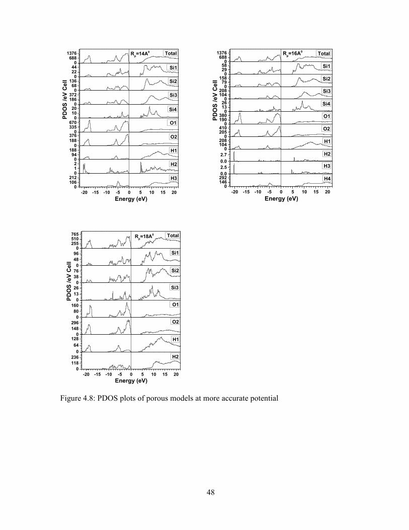
48
Figure 4.8: PDOS plots of porous models at more accurate potential
-20 -15 -10 -5 0 5 10 15 20
0106212
0120
94188
0188376
0335670
010200
186372
068
1360
22440
6881376
Energy (eV)
H3
H2
H1
O2
O1
Si4
Si3
Si2
Si1
Rp=14A
0
PD
OS
/e
V C
ell
Total
-20 -15 -10 -5 0 5 10 15 20
01462920.0
2.5
0.0
2.7
0104208
0205410
0190380
01326
0104208
079
1580
2958
0688
1376
Energy (eV)
H4
H3
H2
H1
O2
O1
Si4
Si3
Si2
Si1
PD
OS
/e
V C
ell
TotalRp=16A
0
-20 -15 -10 -5 0 5 10 15 20
0
118
236
0
64
1280
148
296
0
80
160
0
13
26
0
38
76
0
48
96
0255510765
Energy (eV)
H2
H1
O2
O1
Si3
Si2
Si1
Rp=18A
0
PD
OS
/e
V C
ell
Total
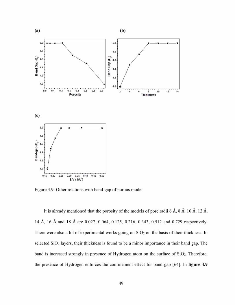
49
(a) (b)
(c)
Figure 4.9: Other relations with band-gap of porous model
It is already mentioned that the porosity of the models of pore radii 6 Å, 8 Å, 10 Å, 12 Å,
14 Å, 16 Å and 18 Å are 0.027, 0.064, 0.125, 0.216, 0.343, 0.512 and 0.729 respectively.
There were also a lot of experimental works going on SiO2 on the basis of their thickness. In
selected SiO2 layers, their thickness is found to be a minor importance in their band gap. The
band is increased strongly in presence of Hydrogen atom on the surface of SiO2. Therefore,
the presence of Hydrogen enforces the confinement effect for band gap [64]. In figure 4.9
50
(a), the band gap obtained from OLCAO calculation is initially constant. Hence, band gap
value remains unchanged up to porosity 21.6%. If we increase the diameter of pore, its
porosity is going to be increased. At that time, the band gap value decreases by increasing the
porosity. The thickness of nanoporous material is also crucial for the OLCAO calculation.
The band gap value of nanoporous increases with increase in its thickness. When thickness
approaches the 40% of model, the band-gap values does not change as shown in figure 4.9
(b). The surface to volume (S/V) ratio is other physical parameters in the study of
nanoporous materials that increases with decrease in pore radius. In OLCAO calculation, the
band gap value increases with increase in S/V initially as shown in figure 4.9 (c). The band
gap value remains unchanged from S/V value corresponding to 60% pore size.
4.2 Discussion
The a-SiO2 NPs models are built from CRN model of a-SiO2 with periodic boundary.
To get the spherical a-SiO2 NPs, it is not possible to cut the part of the structure in the form
of sphere directly from the model. Hence, a point inside the model has to select and the
calculations of the distances of all the atoms from the point are mandatory. Three a-SiO2
models are constructed; model I, model II and model III. In the first model, there is dangling
bonds in the atoms that lie on the surface (shell). These bonds are saturated by H-atoms.
Their electronic structure calculation is done by using the OLCAO package. The calculated
band gap values of a-SiO2 NPs models of radii 12 Å, 15 Å, 18 Å and 20 Å are 2.3 eV, 4 eV, 2
eV and 1.5 eV respectively. It shows that the electronic interaction increases with increase in
the size of the model. Also, by increased in the type of potentials, their band gap values are
found to be 4 eV, 5 eV and 4.2 eV for model of radii 12 Å, 15 Å and 18 Å respectively.
Therefore, the electronic interactions are found to be higher in model of radius 12 Å. In

51
model II, all the Silicon atoms on the surface of a-SiO2 NPs model are bonded to four
Oxygen atoms. From OLCAO calculation, it is found that the band gap values for a-SiO2
NPs of radii 12 Å, 15 Å, 18 Å and 20 Å are 2.5 eV, 2 eV, 1 eV and 1 eV respectively. The
band gap values decreases with increase in size of NPs model. Therefore, the electron
interactions are higher in model of radii 18 Å and 20 Å. The peaks in VB regions are sharper
than the VB of model I and CB are comparable. By increase in type of potentials, their band
gap values become 4.5 eV, 4.5 eV and 1.8 eV for the models of radii 12 Å, 15 Å and 18 Å. It
is not easy to get the trends from these three data. It shows that the electron interactions are
higher in the model of radius 18 Å. The structures in model II are saturated by H-atoms to get
the model III. The band gap values of a-SiO2 NPs models of radii 12 Å, 15 Å and 18 Å are 3.5
eV, 3 eV and 4 eV with some gap states. The electron interactions are higher in model of
radius 15 Å. With increase in potential, these values become 3 eV, 3 eV and 3.75 eV. There is
the possibility of getting the trends of band gap values at higher potentials. Hence, the
electron interactions are found to be higher for smaller models. The band gap values of
original sample of a-SiO2 is 5.8 eV [12] but the electronic properties calculation of a-SiO2
nanoparticles are not found by other researchers yet. Some molecular dynamics (MD) a
calculation on it is found by Vo Van Hoang [32], but the calculations are different than here.
The porous a-SiO2 NPs are also made and their porosities are 0.027, 0.064, 0.125, 0.216,
0.343, 0.512 and 0.729 for the pore of radii of 6 Å, 8 Å, 10 Å, 12 Å, 14 Å, 16 Å and 18 Å
respectively. From OLCAO calculation, the gap states are seen between VB and CB. These
gap states are removed by increasing the type of potentials of atoms. Hence, the band gap of
5 eV, 5 eV, 5 eV, 4.75 eV, 4.5 eV and 4 eV are obtained for pore of radii 8 Å, 10 Å, 12 Å, 14
Å, 16 Å and 18 Å. Their band-gap values remains constant up to 21.6% porosity. After that,

52
their band gap decreases with increase in porosities. The electron interactions are equal for
certain value of the porosity. After that, the interactions increase with increase in their
porosity. Also, their band-gap increases with increase in thickness of porous model and
finally, there is no effect of pore thickness on band-gap. The band-gap increases with
increase in (S/V) and finally the band-gap becomes constant. The change in their surfaces by
making the pores plays the major role in their properties.

53
CHAPTER 5
CONCLUSION AND FUTURE WORK
The a-SiO2 NPs models of different sizes are built and perform their electronic
structure calculation. From the result, the number of atoms in a-SiO2 increases with increase
in their size, which is obvious. The PDOS calculation is crucial in electronic structure
calculations. The trends in band gap are found in model II but it is hard to get trends in other
models at lower potential. The electron interactions are higher for the models with smaller
band gap. At higher potentials, there is the lacking of data because of the restriction of
dimension in OLCAO calculation. In porous model, their porosity increases by increasing the
radii. The most important thing in porous model is about nothingness inside the pore, which
is crucial in many applications. The band-gap values remains constant up to 21.6% porosity.
After that, their band-gap decreases with increase in their porosity and hence electron
interactions increases. Also, the band-gap value increases with increase in thickness and
(S/V). The gap states present in NPs model are removed by increasing the type of potentials.
Therefore, the band gap values normally increases. In SiO2 (amorphous, crystalline and NPS)
model, each silicon is attached to four oxygen and the arrangement of atoms inside the
models are similar. Therefore, the TDOS of a-SiO2 NPs are found to be comparable with the
TDOS of a-SiO2 and p-SiO2.
The a-SiO2 NPs contain pore space, where some important molecules or atoms can be
added. The OLCAO is useful to detect the interaction between the molecules and the NPs
surface. Here, the water molecules are inserted inside the pore and the OLCAO jobs are not
completed yet. The alcohol, gold particle, DNA and proteins can be also inserted inside the

54
pores. The better result might be possible, if this model is relaxed and performs the OLCAO
calculation.

55
APPENDIX A
ABBREVIATIONS
a-SiO2: Amorphous Silica
BO: Bond Order
BL: Bond Length
BZ: Brillouin Zone
CRN: Continuous Random Network
DFT: Density Functional Theory
DNA: Deoxyribo Nucleic Acid
EB: Extended Basis
FB: Full Basis
GTO: Gaussian Type Orbitals
HF: Hartee-Fock
HK: Hohenberg-Kohn
IUPAC: International Union of Pure and Applied Chemistry
KS: Kohn-Sham
LCAO: Linear Combination of Atomic Orbital
LDA: Local Density Approximation
LVB: Lower Valence Band
OLCAO: Orthogonalized Linear Combination of Atomic Orbital
MB: Minimal Basis

56
MD: Molecular Dynamics
NPs: Nanoparticles
OPW: Orthogonalized Plane Wave
PDOS: Partial Density of States
Q*: Effective Charge
ROS: Reactive Oxygen Species
Ry: Rydberg
TDDFT: Time Dependent Density Functional Theory
TDOS: Total Density of States
UVB: Upper Valence Band
XC: Exchange Correlation

57
BIBLIOGRAPHY
1 G. Pacchioni, L. Skuja, and D. Griscom, Defects in SiO2 and Related Dielectrics:
Science and Technology: Science and Technology;[proceedings of the NATO
Advanced Study Institute on Defects in SiO 2 and Related Dielectrics: Science and
Technolgy, Erice, Italy, April 8-20, 2000]. (Springer Science & Business Media,
2000).
2 RAB Devine, J-P Duraud, and E. Dooryhée, Structure and Imperfections in
Amorphous and Crystalline Silicon Dioxide. (John Wiley & Sons Inc, 2000).
3 N. Herbots et al, “The formation of ordered, ultrathin SiO2/Si (1 0 0) interfaces grown
on (1⨯1) Si (1 0 0)” Materials Science and Engineering B 87 303 – 316 (2001)
4 D. J Burgess, E. Duffy, F. Etzler, and A. J. Hickey, "Particle size analysis: AAPS
workshop report, cosponsored by the Food and Drug Administration and the United
States Pharmacopeia," The AAPS Journal 6 (3), 23-34 (2004).
5 A. Nel, T. Xia, L. Mädler, and N. Li, "Toxic potential of materials at the nanolevel,"
Science 311 (5761), 622-627 (2006).
6 S. L. Pal, U. Jana, P.K. Manna, G. P. Mohanta, and R. Manavalan, "Nanoparticle: An
overview of preparation and characterization (2000-2010)," Journal of Applied
Pharmaceutical Science 01 (06), 228-234 (2011).
7 C. Buzea, I. I. Pacheco, and K. Robbie, "Nanomaterials and nanoparticles: Sources
and toxicity," Biointerphases 2 (4), MR17-MR71 (2007).

58
8 Van Doren et al, “Determination of the volume-specific surface area by using
transmission electron tomography for characterization and definition of
nanomaterials” Journal of Nanobiotechnology, 9:17 (2011)
9 G. Oberdörster, E. Oberdörster, and J. Oberdörster, "Nanotoxicology: An emerging
discipline evolving from studies of ultrafine particles," Environmental Health
Perspectives,113, 823-839 (2005).
10 M.Z. Huang and W.Y. Ching, "Electron states in a nearly ideal random network model
of a-SiO2 glass" Phys. Rev. B Condens. Matter,54(8), p. 5299-5308 (1996)
11 N. Li, R. Sakidja, S. Aryal, and W. Y. Ching, "Densification of a continuous random
network model of amorphous SiO2 glass", Physical Chemistry Chemical Physics 16
(4), 1500 (2014)
12 N. Li and W.Y. Ching, "Structural, electronic and optical properties of a large random
network model of amorphous SiO2 glass", Journal of Non-Crystalline Solids 383, 28
(2014).
13 Lizhi Ouyang and Wai-Yim Ching, "Prediction of a high-density phase of SiO2 with a
high dielectric constant", Physica Status Solidi - Rapid Research Letters 242 (7), R64
(2005).
14 M. Z. Huang, L Ouyang and W. Y. Ching " Electron and phonon states in an ideal
continuous random network model of a-SiO2 glass", Physical Review B59, 3540-
3550 (1999)
15 A. D. Maynard, R. J. Aitken, T. Butz, V. Colvin, K. Donaldson, G. Oberdörster, M.
A. Philbert, J. Ryan, A. Seaton, and V. Stone, "Safe handling of nanotechnology,"
Nature 444 (7117), 267-269 (2006).

59
16 C. A. Barnes et al, "Reproducible comet assay of amorphous silica nanoparticles
detect no genotoxicity" Nano Letter, 8(9), pp 3069-3074 (2008)
17 Kyung O. Yu et al, “Toxicity of amorphous silica nanoparticles in mouse keratinocytes”
Journal of Nanoparticle Research, 11(1), pp 15-24 (2009)
18 K. D. Sattler, Handbook of Nanophysics: Clusters and Fullerenes. (CRC Press,
2010).
19 V. V. Hoang, "Molecular dynamics simulation of liquid and amorphous Fe
nanoparticles," Nanotechnology 20 (29), 295703 (2009).
20 J. Zou and X.-lan Chen, "Using silica nanoparticles as a catalyst carrier to the highly
sensitive determination of thiamine," Microchemical Journal 86 (1), 42-47 (2007).
21 H. Zhang, D. R. Dunphy, X. Jiang, H. Meng, B. Sun, D. Tarn, M. Xue, X. Wang, S.
Lin, and Z. Ji, "Processing pathway dependence of amorphous silica nanoparticle
toxicity: colloidal vs pyrolytic," Journal of the American Chemical Society 134 (38),
15790-15804 (2012).
22 V. Kuncser and L. Miu, Size Effects in Nanostructures: Basics and Applications.
(Springer, 2014).
23 Y. D. Glinka, S.-Hsien Lin, and Y.-Tsong Chen, "Two-photon-excited luminescence
and defect formation in SiO 2 nanoparticles induced by 6.4-eV ArF laser light,"
Physical Review B 62 (7), 4733 (2000).
24 Y. D. Glinka, S.-Hsien Lin, and Y.-Tsong Chen, "The photoluminescence from
hydrogen-related species in composites of SiO2 nanoparticles," Applied Physics
Letters 75 (6), 778-780 (1999).

60
25 H. Lord and S. O. Kelley, "Nanomaterials for ultrasensitive electrochemical nucleic
acids biosensing," Journal of Materials Chemistry 19 (20), 3127-3134 (2009).
26 S. Jeong, L. Hu, H. R. Lee, E. Garnett, J. W. Choi, and Y. Cui, "Fast and scalable
printing of large area monolayer nanoparticles for nanotexturing applications," Nano
Letters 10 (8), 2989-2994 (2010).
27 N. Moszner and S. Klapdohr, "Nanotechnology for dental composites ", International
Journal of Nanotechnology 1,1-2 (2004).
28 J.-S. Chang, K. L. B. Chang, D.-F. Hwang, and Z.-L. Kong, "In vitro cytotoxicitiy of
silica nanoparticles at high concentrations strongly depends on the metabolic activity
type of the cell line," Environmental Science & Technology 41 (6), 2064-2068
(2007).
29 J. M. Rosenholm, V. Mamaeva, C. Sahlgren, and M. Lindén, "Nanoparticles in
targeted cancer therapy: mesoporous silica nanoparticles entering preclinical
development stage," Nanomedicine 7 (1), 111-120 (2012).
30 L. Tang and J. Cheng, "Nonporous silica nanoparticles for nanomedicine
application," Nano Today 8 (3), 290-312 (2013).
31 A. Colder, F. Huisken, E. Trave, G. Ledoux, O. Guillois, C. Reynaud, H. Hofmeister,
and E. Pippel, "Strong visible photoluminescence from hollow silica nanoparticles,"
Nanotechnology 15 (3), L1 (2004).
32 V. V. Hoang and T. Odagaki, "Molecular dynamics simulations of simple monatomic
amorphous nanoparticles," Physical Review B 77 (12), 125434 (2008).
33 O. V. Singh, Bio-nanoparticles: Biosynthesis and Sustainable Biotechnological
Implications. (John Wiley & Sons, 2015).

61
34 J. J. Corbalan, C. Medina, A. Jacoby, T. Malinski, and M. W. Radomski,
"Amorphous silica nanoparticles trigger nitric oxide/peroxynitrite imbalance in
human endothelial cells: inflammatory and cytotoxic effects," International Journal of
Nanomedicine 6, 2821 (2011).
35 A. M. Rabea, M. Mohseni, S. M. Mirabedini, and M. H. Tabatabaei, "Surface
analysis and anti-graffiti behavior of a weathered polyurethane-based coating
embedded with hydrophobic nano silica," Applied Surface Science 258 (10), 4391-
4396 (2012).
36 J. Doyle, R. Robertson, G. H. Lin, M. Z. He and A. Gallagher, " Production of high quality amorphous silicon films by evaporative silane surface decomposition ",
Journal of Applied Physics 64, 3215, (1988).
37 W.Y. Ching, "Theoretical studies of the electronic properties of ceramic materials,"
Journal of the American Ceramic Society 73 (11), 3135-3160 (1990).
38 C. Moller and M. S. Plesset, "Note on an approximation treatment for many-electron
systems," Physical Review 46, 618 (1934).
39 T. V. Voorhis and M. Head-Gordon, "Two-body coupled cluster expansions," The
Journal of Chemical Physics 115 (11), 5033-5040 (2001).
40 G. C. Fletcher, The Electron Band Theory of Solids. (North-Holland, 1971).
41 E. Runge and E. K. U. Gross, "Density-functional theory for time-dependent
systems," Physical Review Letters 52 (12), 997 (1984).
42 E. K. U. Gross and R. M. Dreizler, Density Functional Theory. (Springer Science &
Business Media, 2013).

62
43 V. Barone, A. Bencini, and P. Fantucci, Recent Advances in Density Functional
Methods. (World Scientific, 2002).
44 J. M. Seminario, Recent Developments and Applications of Modern Density
Functional Theory. (Elsevier, 1996).
45 D. P. Chong, Recent Advances in Density Functional Methods. (World Scientific,
1995).
46 P. Hohenberg and W. Kohn, "Inhomogeneous electron gas," Physical Review 136
(3B), B864 (1964).
47 C. Fiolhais, F. Nogueira, and M. A. L Marques, A Primer in Density Functional
Theory. (Springer Science & Business Media, 2003).
48 W. Kohn and L. J. Sham, "Self-consistent equations including exchange and
correlation effects," Physical Review 140 (4A), A1133 (1965).
49 R. M. Dreizler and E. K. U. Gross, Density Functional Theory: An Approach to the
Quantum Many-Body Problem, (Springer Berlin, 1990).
50 K. Capelle, "A bird's-eye view of density-functional theory," Brazilian Journal of
Physics 36 (4A), 1318-1343 (2006).
51 D. M. Ceperley and B. J. Alder, "Ground state of the electron gas by a stochastic
method," Physical Review Letters 45 (7), 566 (1980).
52 G. Ortiz, M. Harris, and P. Ballone, "Zero temperature phases of the electron gas,"
Physical Review Letters 82 (26), 5317 (1999).
53 J. P. Perdew and A. Zunger, "Self-interaction correction to density-functional
approximations for many-electron systems," Physical Review B 23 (10), 5048 (1981).

63
54 J. P. Perdew, K. Burke, and M. Ernzerhof, "Generalized gradient approximation made
simple," Errata:(1997) Phys Rev Lett 78, 1396 (1996).
55 W. Y. Ching and C. C. Lin, "Orthogonalized linear combinations of atomic orbitals:
Application to the calculation of energy bands of Si III," Physical Review B 12 (12),
5536 (1975).
56 W. Y. Ching and C. C. Lin, "Orthogonalized linear combinations of atomic orbitals.
II. Calculation of optical properties of polymorphs of silicon," Physical Review B 16
(6), 2989 (1977).
57 W. Y. Ching and C. C. Lin, "Electronic energy structure of amorphous silicon by the
linear combination of atomic orbitals method," Physical Review Letters 34 (19), 1223
(1975).
58 W. Y. Ching, "Microscopic calculation of localized electron states in an intrinsic
glass," Physical review letters 46 (9), 607 (1981).
59 W. Y. Ching and P. Rulis, Electronic Structure Methods for Complex Materials: The
Orthogonalized Linear Combination of Atomic Orbitals. (Oxford University Press,
2012).
60 C. Herring, "A new method for calculating wave functions in crystals," Physical
Review 57 (12), 1169 (1940).
61 E. Clementi and C. Roetti, "Roothaan-Hartree-Fock atomic wavefunctions: Basis
functions and their coefficients for ground and certain excited states of neutral and
ionized atoms, Z≤ 54," Atomic Data and Nuclear Data Tables 14 (3), 177-478 (1974).

64
62 S. Huzinaga, J. Andzelm, M. Klobukowski, E. Radzio-Andzelm, Y. Sakai, and H.
Tatewaki, "Physical sciences data", in Gaussian basis sets for molecular calculations
(Elsevier Amsterdam, 1984), Vol. 16, pp. 299.
63 J. Callaway, Quantum Theory of the Solid State. (Academic Press, 2013).
64 J. M. Wagner et al, Electronic band gap of Si/SiO2: Comparision of ab initio
calculations and photoluminescence measurements, Journal of Vaccum Science
Technology A 25 (6), 1500-1504 (2007)

65
VITA
Chandra Dhakal was born on March 9th, 1981 in Morang, Nepal. He did his schooling
from government school. Mr. Dhakal completed Bachelor degree in Science (B.Sc.) and
Master in Science (M.Sc.) with major in Physics from Tribhuwan University (T.U.),
Kathmandu, Nepal.
Mr. Dhakal came to the United States of America (USA) as a graduate student in the
Department of Physics and Astronomy at University of Missouri-Kansas City (UMKC) in 1st
January 2013. From January 2013, he worked as a Graduate Teaching Assistant (GTA) in
UMKC Physics department. Then, he has joined as a Graduate Research Assistant (GRA) in
Prof. Ching group from August 2014.
Mr. Dhakal is the member of Nepal Physical Society and American Ceramic Society.
He had participated in 57th Mid-West Solid State Conference (MWSSC), Lawrence, Kansas,
2013. Mr. Dhakal had presented the results of his research at 39th International Conference
on Advanced Ceramics and Composites (ICACC), in Orlando, Florida, January 25-30, 2015.