computing in the physical world
TRANSCRIPT

COMPUTING IN THE PHYSICAL WORLD
Roger D. Chamberlain and Ron K. Cytron
Version 0.06 - Draft Chapters 1 to 12

© 2017 Roger D. Chamberlain and Ron K. CytronAll rights reserved

Contents
1 Introduction 1
1.1 Beginnings . . . . . . . . . . . . . . . . . . . . . . . . . . . . . 1
1.1.1 Why? . . . . . . . . . . . . . . . . . . . . . . . . . . . . 1
1.1.2 The Arduino Platform . . . . . . . . . . . . . . . . . . . 2
1.2 Digital Systems . . . . . . . . . . . . . . . . . . . . . . . . . . . 3
1.3 Authoring Programs . . . . . . . . . . . . . . . . . . . . . . . . 7
1.4 Integrated Development Environments . . . . . . . . . . . . . . 8
1.5 Interacting with the Physical World . . . . . . . . . . . . . . . 9
1.6 The Role of Design . . . . . . . . . . . . . . . . . . . . . . . . . 9
2 Digital Output 11
2.1 Why Digital Outputs? . . . . . . . . . . . . . . . . . . . . . . . 11
2.2 Software . . . . . . . . . . . . . . . . . . . . . . . . . . . . . . . 12
2.3 Example Digital Output Use Cases . . . . . . . . . . . . . . . . 13
2.3.1 LED Indicator . . . . . . . . . . . . . . . . . . . . . . . 13
2.3.2 Buzzer . . . . . . . . . . . . . . . . . . . . . . . . . . . . 14
2.3.3 Relay . . . . . . . . . . . . . . . . . . . . . . . . . . . . 15
3 Digital Input 17
3.1 Why Digital Inputs? . . . . . . . . . . . . . . . . . . . . . . . . 17
3.2 Hardware . . . . . . . . . . . . . . . . . . . . . . . . . . . . . . 18
3.3 Software . . . . . . . . . . . . . . . . . . . . . . . . . . . . . . . 19
3.4 Example Digital Input Use Cases . . . . . . . . . . . . . . . . . 20
3.4.1 Switch . . . . . . . . . . . . . . . . . . . . . . . . . . . . 20
3.4.2 Proximity Detector . . . . . . . . . . . . . . . . . . . . . 20
3.5 Debouncing Mechanical Contacts . . . . . . . . . . . . . . . . . 20
3.6 Hardware vs. Software . . . . . . . . . . . . . . . . . . . . . . . 22
4 Analog Output 27
iii

Contents
4.1 Why Analog Outputs? . . . . . . . . . . . . . . . . . . . . . . . 27
4.2 Relating Analog Output Values to Physical Reality . . . . . . . 28
4.3 Software . . . . . . . . . . . . . . . . . . . . . . . . . . . . . . . 30
4.4 Example Analog Output Use Cases . . . . . . . . . . . . . . . . 30
4.4.1 Motor Speed . . . . . . . . . . . . . . . . . . . . . . . . 30
4.4.2 Loudness . . . . . . . . . . . . . . . . . . . . . . . . . . 31
5 Analog Input 33
5.1 Why Analog Inputs? . . . . . . . . . . . . . . . . . . . . . . . . 33
5.2 Counts to Engineering Units . . . . . . . . . . . . . . . . . . . . 34
5.2.1 Input Range and Linear Transformation . . . . . . . . . 34
5.3 Software . . . . . . . . . . . . . . . . . . . . . . . . . . . . . . . 36
5.4 Example Analog Input Use Cases . . . . . . . . . . . . . . . . . 37
5.4.1 Temperature . . . . . . . . . . . . . . . . . . . . . . . . 37
5.4.2 Level . . . . . . . . . . . . . . . . . . . . . . . . . . . . . 38
5.4.3 Acceleration . . . . . . . . . . . . . . . . . . . . . . . . . 40
6 Timing 43
6.1 Execution Time . . . . . . . . . . . . . . . . . . . . . . . . . . . 44
6.2 Controlling Time . . . . . . . . . . . . . . . . . . . . . . . . . . 45
6.3 Delta Time . . . . . . . . . . . . . . . . . . . . . . . . . . . . . 47
6.4 Multiple Time Periods . . . . . . . . . . . . . . . . . . . . . . . 49
7 Design Patterns 53
7.1 Finite-State Machines . . . . . . . . . . . . . . . . . . . . . . . 53
7.2 Polling and Interrupts . . . . . . . . . . . . . . . . . . . . . . . 60
7.2.1 Polling . . . . . . . . . . . . . . . . . . . . . . . . . . . . 60
7.2.2 Interrupts . . . . . . . . . . . . . . . . . . . . . . . . . . 65
7.2.3 Discussion . . . . . . . . . . . . . . . . . . . . . . . . . . 66
8 Information Representation 69
8.1 Numbers . . . . . . . . . . . . . . . . . . . . . . . . . . . . . . . 69
8.1.1 Brief History of Number Systems . . . . . . . . . . . . . 69
8.1.2 Positional Number Systems . . . . . . . . . . . . . . . . 75
8.1.3 Supporting Negative Numbers . . . . . . . . . . . . . . 79
8.1.4 Integer Data Types in Programming Languages . . . . . 83
8.1.5 Fractional Numbers . . . . . . . . . . . . . . . . . . . . 84
8.1.6 Real Numbers . . . . . . . . . . . . . . . . . . . . . . . . 85
8.2 Text: Characters and Strings . . . . . . . . . . . . . . . . . . . 88
8.2.1 ASCII . . . . . . . . . . . . . . . . . . . . . . . . . . . . 88
iv

Contents
8.2.2 Unicode . . . . . . . . . . . . . . . . . . . . . . . . . . . 90
8.2.3 String Representations . . . . . . . . . . . . . . . . . . . 91
8.3 Images . . . . . . . . . . . . . . . . . . . . . . . . . . . . . . . . 92
8.3.1 Monochrome Images . . . . . . . . . . . . . . . . . . . . 93
8.3.2 Color Images . . . . . . . . . . . . . . . . . . . . . . . . 93
9 User Interaction 95
9.1 Visual Display . . . . . . . . . . . . . . . . . . . . . . . . . . . 95
9.1.1 Display Technologies . . . . . . . . . . . . . . . . . . . . 95
9.1.2 7-segment Displays . . . . . . . . . . . . . . . . . . . . . 96
9.1.3 Pixel-oriented Displays . . . . . . . . . . . . . . . . . . . 101
9.2 Sound . . . . . . . . . . . . . . . . . . . . . . . . . . . . . . . . 104
9.3 Other Senses . . . . . . . . . . . . . . . . . . . . . . . . . . . . 104
9.4 User Input . . . . . . . . . . . . . . . . . . . . . . . . . . . . . . 104
9.5 User Interface Design . . . . . . . . . . . . . . . . . . . . . . . . 104
10 Computer Architecture 105
10.1 Basic Computer Architecture . . . . . . . . . . . . . . . . . . . 105
10.1.1 Architecture Components . . . . . . . . . . . . . . . . . 105
10.1.2 Fetch-Decode-Execute Cycle . . . . . . . . . . . . . . . 107
10.2 Instruction Set Architecture (ISA) . . . . . . . . . . . . . . . . 107
10.2.1 Register File . . . . . . . . . . . . . . . . . . . . . . . . 108
10.2.2 Memory Model . . . . . . . . . . . . . . . . . . . . . . . 109
10.2.3 Instruction Set . . . . . . . . . . . . . . . . . . . . . . . 113
10.2.4 Operating Modes . . . . . . . . . . . . . . . . . . . . . . 120
11 Assembly Language 121
11.1 Machine Instructions . . . . . . . . . . . . . . . . . . . . . . . . 121
11.2 Assembly Language Instructions . . . . . . . . . . . . . . . . . 122
11.3 Labels and Symbols, Constants and Numbers . . . . . . . . . . 123
11.4 Assembly Language Pseudo-operations . . . . . . . . . . . . . . 124
11.4.1 Sections . . . . . . . . . . . . . . . . . . . . . . . . . . . 124
11.4.2 Data Section Pseudo-ops . . . . . . . . . . . . . . . . . 124
11.4.3 Text Section Pseudo-ops . . . . . . . . . . . . . . . . . . 125
11.4.4 Macros . . . . . . . . . . . . . . . . . . . . . . . . . . . 126
11.5 Authoring in Assembly Language . . . . . . . . . . . . . . . . . 127
11.5.1 Accessing Data . . . . . . . . . . . . . . . . . . . . . . . 127
11.5.2 Control Flow Templates . . . . . . . . . . . . . . . . . . 132
11.6 Interfacing with C . . . . . . . . . . . . . . . . . . . . . . . . . 137
11.6.1 Calling Conventions . . . . . . . . . . . . . . . . . . . . 137
v

Contents
11.6.2 Calling C Routines from Assembly Language . . . . . . 14011.6.3 Calling Assembly Language Routines from C . . . . . . 141
12 Computer to Computer Communications 14312.1 Stream Concepts . . . . . . . . . . . . . . . . . . . . . . . . . . 144
12.1.1 Streams on the Microcontroller . . . . . . . . . . . . . . 14412.2 Delivery of Streams . . . . . . . . . . . . . . . . . . . . . . . . . 14512.3 Protocols . . . . . . . . . . . . . . . . . . . . . . . . . . . . . . 145
12.3.1 Byte Delivery . . . . . . . . . . . . . . . . . . . . . . . . 14512.3.2 Delivering Larger Data Items . . . . . . . . . . . . . . . 14612.3.3 Messages . . . . . . . . . . . . . . . . . . . . . . . . . . 147
12.4 Sending Messages: Composition . . . . . . . . . . . . . . . . . . 14912.5 Receiving Messages: Parsing . . . . . . . . . . . . . . . . . . . . 150
13 Conclusions 153
A Languages 155
B Simple Introduction to Electricity 157
C Base Conversions 159C.1 Convert Base A to Base B using Base B Math . . . . . . . . . 159C.2 Convert Base A to Base B using Base A Math . . . . . . . . . 160
Bibliography 165
Index 167
vi

1 Introduction
1.1 Beginnings
Years ago, computers were big bulky things that consumed entire rooms, some-times entire buildings, to house them. Users accessed them by first schedulingtime with the owner of the computer (only one program at a time could run)and then coming to the computer room to manually input their program andinput data, perform a run, and examine the outputs. The program mighthave been stored on a paper tape, with holes punched in it to represent thedetails of the machine instructions. The output invariably was on a stream offan-fold paper.
We have we come a long ways. Computers are now ubiquitous in our lives.We carry them around in our pockets, use them to interact with friends (bothclose friends we see every day and far-off friends we almost never see otherthan via social media), and trust them to monitor our health (keeping trackof our heart rate and how many steps we make each day).
This text will focus primarily on the latter of these three examples ofubiquity. In the modern world, computers are no longer relegated to runningprograms that have input provided by a paper tape and outputs printed onfan-fold paper. Nor are they relegated to the more recent circumstance ofinput provided by a keyboard and outputs presented on a desktop screen. No,modern computers frequently take their inputs directly from measurementsmade from the physical world, and often control aspects of that same physicalworld.
1.1.1 Why?
We are interested in computers that interact with the real physical world be-cause those computers can do so much more than a computer that is relegatedto only have input from humans and output to humans. When a computerthat is held in the palm of our hand includes a microphone, a speaker, and a
1

1. Introduction
cellular radio, it becomes a phone. When a computer controls the timing ofspark plug firings in an internal combustion engine, the engine can run moreefficiently, increasing engine power and decreasing fuel consumption.
The examples above are possible when the computer senses one or moreproperties of the physical world around it and is able to effect change in thephysical world as well. In this book, we describe how computers can interactwith the real world, and what are the fundamental principles involved inbuilding and programming computer systems that have these capabilities.
1.1.2 The Arduino Platform
The microcontroller that we will use to illustrate the topics we cover is theAVR microcontroller manufactured by Atmel, specifically the ATmega328P.It is an 8-bit processor, and it has 14 digital input/output pins (of which 6can be used as pulse-width modulated analog outputs), 6 analog input pins(supporting a 10-bit A/D converter), 32 KBytes of program memory, and2 KBytes of data memory. The term microcontroller is frequently used for achip that contains not only the processor, but additional components as well,such as I/O and built-in memory.
The ATmega328P microcontroller is used on the Arduino Uno, one of aline of experimental boards used extensively by hobbyists. Other boards inthe Arduino family use other microcontrollers in the AVR line (all of whichshare the same instruction set, varying in the number of I/O pins, memory,etc.).
All of the Arduino boards can be programmed using a variant of the Clanguage. Software development is supported via an integrated developmentenvironment (IDE) that is open source and free to use. Arduino programs arecalled sketches in the hobbyist community, and we will follow that convention.Figure 1.1 shows a very simple sketch that prints a message to the desktopPC.
Every Arduino sketch has at least two components, setup() and loop().The code that is in setup() is executed once, at the beginning of the run, andthe code that is in loop() is executed repeatedly thereafter. A sketch doesnot terminate, but runs until stopped by the user (e.g., by issuing a reset).
Appendix A describes some of the idiosyncrasies of the Arduino C variantthat is supported. It is also possible to author programs using the AVRassembly language, a topic that will be discussed in Chapter 10. All of theprogram code that we use in examples has been tested on the Arduino Unoplatform. However, the changes needed for other Arduino boards are quitesmall (e.g., altering the specific pins used for particular I/O functions).
2

1.2. Digital Systems
void setup() {
Serial.begin(9600); // setup communications
Serial.println("Hello world!"); // print message
}
void loop() {
}
Figure 1.1: Hello world example sketch.
1.2 Digital Systems
In all digital systems, information is represented in binary form. The binarynumber system is one in which there are only two possible values for eachdigit: 0 and 1. At different times and for different purposes the 1s and 0smean different things. One useful meaning is for 1 to represent TRUE and 0to represent FALSE, allowing us to reason using propositional calculus.
Let’s say we are studying at a university that requires all of its students tohave taken one or more courses in economics prior to graduation. We will fur-ther assume that the economics requirement is to study both microeconomics(how individuals and organizations make economic decisions that effect them-selves) and macroeconomics (how economies as a whole operate at a largescale, e.g., at the level of a country). Given the availability of the followingthree courses:
Econ A Introduction to MicroeconomicsEcon B Introduction to MacroeconomicsEcon C Economics Survey: Micro and Macro
we use the symbol A to represent a student having completed Econ A, thesymbol B to represent the student having completed Econ B, and C to rep-resent the completion of Econ C. Each of these symbols (A, B, or C) cantake on the value 0 or 1, and cannot take on any other value. Under theseconstraints, these symbols are said to be Boolean valued (the name comingfrom George Boole, 19th century mathematician, who is often considered tobe the father of modern digital logic [2]).
If the symbol E represents our student having completed the economicsrequirement, we can write down an equation that embodies this definition:
E = (A AND B) OR C (1.1)
3

1. Introduction
where the AND operator and the OR operator are described with precisionbelow, but have meaning that is consistent with the normal English definitionsof the terms. In English, we would say that the student needs to take bothEcon A and Econ B (one providing microeconomics knowledge and the otherproviding macroeconomics knowledge) or the student needs to take Econ C(which provides both micro- and macroeconomics training). Clearly, the equa-tion can be interpreted by someone reading it to mean exactly the same thing.
The AND operator and the OR operator are two of three basic logicaloperations supported in Boolean algebra, the third being the NOT operator.Boolean algebra is a mathematical framework that allows us to formally reasonabout Boolean valued variables, operations on those variables, and equationsthat utilize those operations. Equation (1.1) is an example of an equation inBoolean algebra.
We will define these three operations (AND, OR, NOT) through completeenumeration of all the possible combinations of values. This is a technique thatis available to us primarily because the number of combinations isn’t all thatlarge. Since each variable can only have two values, things stay at reasonablesizes as long as the number of variables also stays small. It is common to callthe tables that show all possible values truth tables. (It should be clear whythis name is used, given the frequent interpretation, which we are using here,of 0 representing FALSE and 1 representing TRUE.) Table 1.1 shows the truthtables for the AND operation, the OR operation, and the NOT operation.
x y z
0 0 00 1 01 0 01 1 1
x y z
0 0 00 1 11 0 11 1 1
x z
0 11 0
(a) (b) (c)
Table 1.1: (a) AND truth table. (b) OR truth table. (c) NOT truth table.
As mentioned above, the formal definitions of the operations, as shownin Table 1.1, closely follow the normal English language usage of the wordsused to name the operations. The AND operation yields a 1 only when bothinputs are 1, the OR operation yields a 1 when either input is a 1, and theNOT operation yields a 1 when its single input isn’t a 1. It is important tonote, however, that these formal definitions are how one resolves potentialambiguity. In English, the word “or” can, in some circumstances, mean “x ory but not both x and y together,” but this is not the meaning defined in the
4

1.2. Digital Systems
truth table.
Using the symbols frequently utilized by logicians, Equation (1.1) can berewritten as follows:
E = (A ∧B) ∨ C (1.2)
where the ∧ symbol is used to represent the AND operation and the ∨ symbolis used to represent the OR operation.
Just to illustrate that there are many ways to write down the same no-tion, the more common notation used in computer engineering and electricalengineering disciplines is to use the traditional addition symbol (+) for ORand the traditional multiplication notation (either · or simply juxtaposition)for AND. Using this approach, the equation now looks like this,
E = (A ·B) + C (1.3)
or this,
E = AB + C (1.4)
where Equation (1.4) has also taken advantage of the normal convention thatmultiplication takes precedence over addition (in this case, AND takes prece-dence over OR) to drop the parenthesis from the equation.
Since there are only 3 variables on the right-hand side of the equation, andeach variable can have only two values, we can examine this equation with thehelp of a truth table. Recall that in a truth table, all possible combinationsof the input variables are listed, one combination per row. In the truth tablefor an expression, different columns are frequently used to represent differentsubexpressions (or the final value). The truth table for Equation (1.4) is shownin Table 1.2.
A B C AB AB + C E
0 0 0 0 0 00 0 1 0 1 10 1 0 0 0 00 1 1 0 1 11 0 0 0 0 01 0 1 0 1 11 1 0 1 1 11 1 1 1 1 1
Table 1.2: Truth table showing all possible conditions for each input variablein Equation (1.4).
5

1. Introduction
It is also possible to build a physical system that implements the logicalreasoning encoded into Equation (1.4), and Equations (1.1) to (1.3) as well.Figure 1.2 shows the schematic diagram symbols for each of the 3 operations.The physical implementations of these symbols are called gates, and the logicalvalues are encoded as voltages on input and output wires (typically, a HIGHvoltage represents a 1 and a LOW voltage represents a 0).
(a) (b) (c)
Figure 1.2: (a) AND gate. (b) OR gate. (c) NOT gate.
Using these logic gates as building blocks, Figure 1.3 shows a schematicdiagram for a circuit that implements Equation (1.4). The inputs A, B, andC on the left encode whether or not the student has taken the courses Econ A,Econ B, and Econ C, respectively. The output E on the right encodes whetheror not the student has met the economics requirement for the degree.
Figure 1.3: Gate-level schematic diagram of circuit that implements economicscourse requirement check.
Figure 1.3 is a simple example of an application-specific computation. Itdoes a great job of its assigned application (checking whether or not a studenthas met his/her economics requirement); however, it doesn’t really do muchof anything else. Most of the time, we are interested in more general purposecomputing devices. These are ones that can compute not only the results ofEquation (1.4), but many other computations as well.
Computers are simply digital systems that have been engineered to domultiple tasks instead of an individual task. We provide them with a program,which gives specific instructions for the computer to execute. Computers comein many sizes, from small enough to fit in a smart watch, to large enough tofill a room; however, they all do exactly what they are told. They executespecific instructions given to them in the form of a program.
6

1.3. Authoring Programs
1.3 Authoring Programs
In order to provide a computer with a program, we must first design thatprogram, and author it in some language that the computer can understand.Many are familiar with high-level languages, such as C, C++, Java, etc., thatare frequently used to author programs. We will write in a variant of the Clanguage as we develop programs for the AVR microcontroller.
These languages, however, are not the language of the processor itself. In-stead, the processor directly executes machine language, a much lower-levellanguage that directly encodes the specific instructions to be executed, one af-ter the other, by the computer. Machine language instructions are representedas a string of 1s and 0s stored in the memory of the processor.
It is possible to author programs at the same conceptual level as machinelanguage. To do this, we use assembly language, which is a human-readableand -writable language that has a one-to-one relationship with machine lan-guage. Instead of representing instructions directly as 1s and 0s, however,assembly language uses mnemonic names for instructions.
Figure 1.4 shows the relationship between machine language, assemblylanguage, and high-level languages. Each assembly language instruction cor-responds to an individual machine language instruction (in a one-to-one re-lationship). Each high-level language statement corresponds to multiple ma-chine language instructions (in a one-to-many relationship).
Figure 1.4: Relationship between languages. Assembly language (asm), ma-chine language (ml), and high-level language (HLL).
Various software tools are used to translate between languages. Tradition-ally, a software tool that translates assembly language programs into machinelanguage is called an assembler . The tool that translates a high-level lan-guage program into either assembly language or machine language is called a
7

1. Introduction
compiler . Both are built into an integrated development environment (IDE).
1.4 Integrated Development Environments
A practitioner in any discipline would tell you that having the right tool for agiven task improves the efficiency and enjoyment of completing the task, andthat the quality of the completed task is improved as well. The developmentof software, hardware, or co-designed systems is often a complex undertaking,involving multiple developers, shifting goals and deliverables, and limited re-sources. Integrated development environments have emerged as the platformof choice for developers because they facilitate the creation of quality systems.
The process of authoring a program, as described above, involves differentcomponents of what is typically called the development stack. Each layer ofthe stack plays some role in the creation of the end product. An IntegratedDevelopment Environment (IDE) allows the layers of that stack to interoperatebeneficially and to provide useful feedback to the product’s developers. Hereare some examples of the features provided by an IDE:
• The source code of the project can be viewed and edited efficiently. Thesyntax is typically formatted consistently and highlighted to improvereadability. Color and font may distinguish programming language ele-ments (if, then, else) from program-specific concepts (local variables,data types, packages).
As an example, consider changing a particular method named foo tobar throughout an entire application. A text editor alone could findoccurrences of foo, but some of those might be variable names andsome may occur in comments. It requires the integration of a compilerwith the editor to accomplish a method rename.
• A debugger may help diagnose the cause of a program’s undesirablebehavior. The IDE can facilitate tracing the program’s behavior andrelating it to variables, methods, and statements as seen in the editor.
• When a system is tested, one criterion for completeness concerns thecoverage of a program’s statements. Testing in an IDE can show linesof a project that have not been exercised by existing tests.
IDEs typically simplify importing code from a shared repository and exportingthe results of modifications back to the repository. IDEs such as eclipse offerservices and interfaces that allow the open-source community to introduce
8

1.5. Interacting with the Physical World
new tools into the IDE that integrate well with tools and components alreadypresent.
1.5 Interacting with the Physical World
We are interested in computers that interact with the real world. They takemeasurements of physical phenomena, perform some computation, and op-tionally trigger some physical action. Examples of computers that performthese types of functions include the temperature and humidity controller inan environmental chamber, the embedded systems that control the flight sur-faces (e.g., rudder, elevators, ailerons) in a fighter jet, and the FitbitTM thatyou might be wearing on your wrist right now.
To accomplish these tasks, the computer cannot be limited to a keyboardfor input and a screen for output. Instead, it must interact directly with thephysical world. In the next 4 chapters, we will examine 4 specific mechanismsthat allow interaction between the computer and the real world.
1.6 The Role of Design
We are surrounded by objects, mechanisms, and interfaces that are the resultof design, but ironically design is most successful when it is least apparent.When you approach a door with the intention of opening it, how do you knowwhether to push or pull on the door’s handle? A well designed door makessuch interactions obvious, to the extent that its users express no wonder atits ease of operation.
Practitioners of computer science and engineering are often faced withdesign choices and decisions that affect the efficiency, security, and usabilityof their products. The most effective designs take into account the context inwhich a product will be deployed as well as considerations of how the product’susage might evolve over time. Even our simple door is not so simple: if thedoor has a latching mechanism, should it be operated via a simple knob?A round, smooth knob is less likely to tangle with clothing, but requiressome dexterity and hand strength to operate. A lever can be operated moreuniversally, but it could also interact unpredictably with belt loops or pantspockets.
The point here is that with most design, there is no absolutely right orwrong answer. There are tradeoffs that must be considered, and the value ofa given design is measured in terms of its suitability for a particular environ-ment or context. Throughout this text, you will be exposed to design choices,
9

1. Introduction
evaluations, and patterns. While you could study this material without anyconsideration of design, engineers continually grapple with design. By intro-ducing design this early in your studies, you can begin to see the challengesand rewards of considering design alternatives as you develop solutions.
10

2 Digital Output
A digital output is pretty much exactly like you would expect, given thenormal English definitions of “digital” and “output.” There are only twopossible values, which we will denote as 0 and 1, and the computer is sendingone of those two values out into the physical world.
Electrically, one of the pins of the microcontroller is establishing a LOWvoltage (for an output value of 0) or a HIGH voltage (for an output value of1). To be safe (and for a number of other reasons), actually neither outputvalue is a high enough voltage that we need to be concerned about touchingit. The HIGH voltage mentioned above is approximately 5 V above the GNDpotential (for a 5 V microcontroller, it would be about 3.3 V on a 3.3 Vmicrocontroller), and the LOW voltage is approximately 0 V above the GNDpotential (i.e., it is at the same voltage as GND). If you are unfamiliar withthe concept of voltage, see Appendix B.
So, if we have a pin on the microcontroller that can establish a HIGHvoltage or a LOW voltage out, what good is that? Let’s examine what adigital output is actually good for.
2.1 Why Digital Outputs?
This book is about computing in the physical world, and a digital output isthe simplest way that a computer can influence the world around it. If thecomputer is controlling the light in a room, a digital output is used to turn thelight on or off. If the computer is communicating the presence (or absence)of an alarm, a digital output is used to turn the alarm on or off. This is trueif the alarm is a buzzer or if the alarm is some large visual indicator. If thecomputer is controlling the heating element in an oven, a digital output canbe used to turn the heating element on or off. If the computer is controllinga conveyor belt, a digital output is used to turn the conveyor belt on or off.
The pattern should be pretty obvious. Whenever there are two output
11

2. Digital Output
options, the physical effect can be controlled via a digital output. All that isrequired is circuitry that transforms the output voltage from the microcon-troller (either LOW or HIGH) into the actuator control desired in the realworld.
2.2 Software
To control a digital output pin from software, we must first configure the pinas a digital output. Most of the pins on the microcontroller serve multiplepurposes (e.g., digital output and digital input), and it is our responsibilityto configure the pin prior to use.
Configuring a digital output pin is accomplished using the pinMode() func-tion. It takes two arguments, the first is an int identifying the pin numberand the second is the the constant OUTPUT indicating that the pin is now adigital output.
Once the pin has been configured, the digitalWrite() function is usedto set the output HIGH or LOW. A HIGH output corresponds to 5 V (for a 5 Vmicrocontroller) and a LOW output corresponds to 0 V.
Figure 2.1 gives an example sketch that toggles a digital output at 1 Hz(high for 0.5 s, low for 0.5 s, high for 0.5 s, etc.).
const int doPin = 17; // digital output pin is 17
void setup() {
pinMode(doPin, OUTPUT); // set pin to digital output
}
void loop() {
digitalWrite(doPin, HIGH); // set the output HIGH
delay(500); // wait for 0.5 s (500 ms)
digitalWrite(doPin, LOW); // set the output LOW
delay(500); // wait for 0.5 s
}
Figure 2.1: Example digital output sketch.
12

2.3. Example Digital Output Use Cases
2.3 Example Digital Output Use Cases
2.3.1 LED Indicator
One of the simplest digital output devices one can imagine is a light that iseither on or off. LEDs (light emitting diodes) are a common light source thatare easy to control from a microcontroller’s digital output pin. Figure 2.2shows the schematic for controlling a single LED from pin 17 of the micro-controller (there is nothing special about pin 17, other than it must be usableas a digital output pin and it is the pin number from the example code inFigure 2.1).
Figure 2.2: Schematic diagram of digital output controlled LED with activehigh control polarity. The anode is the topmost terminal of the LED and thecathode is the bottom terminal.
If the sketch from Figure 2.1 is executed on the microcontroller that hasthe schematic from Figure 2.2 constructed, the LED will light up in responseto the digitalWrite(doPin,HIGH) call. This is because a positive voltage ispresented to the anode of the LED and zero volts are presented to the cathode(which is at GND potential). Generally, the HIGH voltage out of the micro-controller (+5 V) is too large for the LED, and it is possible to damage theLED or the microcontroller, so we use the current limiting resistor to ensurethat does not happen. One half-second later, the digitalWrite(doPin,LOW)
call will cause the LED to become dark. With zero volts on the anode andzero volts on the cathode, the LED will not light.
In this example, when the digital output is HIGH, the LED is on, and whenthe digital output is LOW, the LED is off. This design choice is commonlycalled active high, meaning that the action (here, lighting the LED) happenswhen the signal is high. That is a completely arbitrary choice, however. Con-
13

2. Digital Output
sider the schematic diagram shown in Figure 2.3, which gives an alternativedesign. In this case, the digital output is connected to the cathode side of theLED, and the anode side goes to +5 V. With this design, an output HIGH,gives 5 V on both the anode and the cathode of the LED, and it will stay dark.An output LOW, on the other hand, provides 0 V to the cathode side of theLED, which will cause it to light up. This design choice is commonly calledactive low . As a result of the alternative schematic connections, the operationof the light as a function of the digital output polarity has been reversed.
Figure 2.3: Schematic diagram of digital output controlled LED with activelow control polarity. In this case, the anode of the LED is tied to +5 V andthe cathode is tied to the digital output pin.
What this shows is that while there is a direct one-to-one relationship be-tween the digital output value (HIGH or LOW) and the LED being controlled(on or off), the mapping between these two is determined by the design of theelectrical circuit(s) that connect them.
2.3.2 Buzzer
A commonly used technique to generate an audio signal is through the use ofa buzzer. When a voltage is applied across the buzzer, it makes a sound, andis silent otherwise. This is a perfect example of a digital output.
The schematic diagram of a buzzer output is shown in Figure 2.4. Whenthe digital output is HIGH, the buzzer makes sound, and when the digitaloutput is LOW, the buzzer is silent.
14

2.3. Example Digital Output Use Cases
Figure 2.4: Schematic diagram of digital output controlled buzzer.
2.3.3 Relay
A relay is another device that can be controlled with a digital output. A relayhas a low-voltage control side that turns on or turns off a set of mechanicalcontacts that can be used to control high-voltage devices, such as devices thatuse 110 V power from the wall socket. This might include motors, pumps,heating elements, etc.
15


3 Digital Input
Probably the simplest form of interaction between a computer and the physicalworld is for the computer to sense (i.e., measure) some property of the world.Given that the internal representation of whatever thing we measure is going tobe binary, the easiest things to measure are those that are readily representedin a binary system. Sensing opportunities that have this property are thosefor which there are only two options.
For example, consider a proximity detector that is placed on an assemblyline. Its job is to determine whether or not there is a manufactured widgetin front of it (i.e., in the proximity of the sensor). The answer is either “yes”or “no.” Another example would be an emergency stop button on that sameassembly line. In this case, a human is either pressing the button or not.Again, the answer is either “yes” or “no.”
For each of these possible inputs, the information present can be repre-sented inside the computer using a single binary bit, a 0 or a 1. The meaningof 0 or 1 will depend upon the specifics of the measurement being made.E.g., for the proximity detector, 0 might mean “not present” and 1 mightmean “present.” Likewise, for the emergency stop button, 0 might mean “notpressed” and 1 might mean “pressed.”
3.1 Why Digital Inputs?
Note that the action that the computer will take in response to the examplesensor inputs above might very well be radically different. When the com-puter senses the proximity detector input transitioning from “not present” to“present,” it might simply increase an internal counter that is keeping track ofinventory. Alternatively, when the computer senses the emergency stop but-ton transitioning from “not pressed” to “pressed,” its responsibility at thatpoint is likely to halt the motion of the assembly line (which it would likely dovia the use of a digital output). The bottom line is that the computer cannot
17

3. Digital Input
do any of these things unless it is making the relevant measurement in thefirst place. Measuring some property of the physical world has enabled thecomputer to do things it otherwise could not do.
3.2 Hardware
While the specific hardware required for any particular digital measurement isclearly dependent upon the type of measurement that is being made, a com-mon digital input is a pushbutton or a switch. Figure 3.1 shows a commonlyused circuit for interfacing a pushbutton to a microcontroller input pin.
Figure 3.1: Schematic diagram of circuit that interfaces a pushbutton inputto a microcontroller digital input pin.
In the figure, when the pushbutton is not being pressed, it creates an opencircuit (i.e., no current can flow), because the input pin of the microcontrolleris in a high impedance state when configured as an input, and the resistor pullsthe voltage at the input pin up to +5 V (the power supply voltage). Whenthe pushbutton is being pressed, it shorts the input pin to 0 V (ground). Asa result, the input pin has a low voltage potential when the button is pressedand a high voltage when the button is not pressed.
This is an example of an active low design. The action is pressing thebutton, which yields a low input voltage on the microcontroller input. It isentirely reasonable to implement an active high design as well, which wouldinvolve swapping the positions of the switch and the resistor in Figure 3.1.
18

3.3. Software
3.3 Software
As stated in Chapter 2, most of the pins on the microcontroller serve multiplepurposes, and it is our responsibility to configure the pin prior to use. To reada digital input in software, we must first configure the pin as a digital input.
Configuring a digital input pin is accomplished using the pinMode() func-tion. It takes two arguments, the first is an int identifying the pin numberand the second is an int indicating the pin mode. For the mode, the constantsINPUT or INPUT PULLUP indicate the pin is to be a digital input.
The typical use case is to use the INPUT pin mode. This would be theappropriate mode to use for the circuitry depicted in Figure 3.1. However,the use of a switch (or some other circuit) to actively pull the voltage low incombination with a resistor that passively pulls the voltage high (i.e., an activelow design) is a use case that is fairly common. As a result, microcontrollersoften provide the resistor built-in to the chip, and the INPUT PULLUP modetells the microcontroller to enable the built-in pullup resistor. In this way, theexternal resistor of Figure 3.1 is no longer needed, as the resistor is internalto the microcontroller. Because of the availability of built-in pullup resistorsin many microcontrollers, active low inputs are a much more prevalent designchoice, versus the active high alternative.
Once the pin has been configured, the digitalRead() function is used toperform the actual reading of the input. If the voltage at the pin is approxi-mately 5 V (relative to the GND potential), then the digitalRead() functionreturns the constant value HIGH (which is defined as a 1). If the voltage atthe pin is approximately 0 V, the the digitalRead() function returns theconstant value LOW (which is defined as a 0). If the voltage at the pin is nearthe midpoint (≈ 2.5 V), the return value is indeterminate, and either a HIGH
or a LOW might result.1
Figure 3.2 gives an example sketch that repeatedly reads from a digitalinput, writes the value to a digital output, and prints the value. Note thatin the sketch, value is declared as an int. This is because digitalRead()
returns HIGH or LOW, which are constants of type int.
1Actually, there are two values specified in the data sheet of the microcontroller thatmore precisely describe how voltages at the input pin are interpreted. Any voltage less thanVIL will return a 0 in software and any voltage greater than VIH will return a 1 in software.Voltages between VIL and VIH give indeterminate results.
19

3. Digital Input
const int diPin = 16; // digital input pin is 16
const int doPin = 17; // digital output pin is 17
int value = LOW; // input value
void setup() {
pinMode(diPin, INPUT); // set pin to digital input
pinMode(doPin, OUTPUT); // set pin to digital output
Serial.begin(9600);
}
void loop() {
value = digitalRead(diPin); // read the input
digitalWrite(doPin, value); // set the output to value
Serial.print("value = ");
Serial.println(value);
}
Figure 3.2: Example digital input sketch.
3.4 Example Digital Input Use Cases
3.4.1 Switch
The interfacing of a mechanical switch to a microcontroller digital input wasdescribed in Section 3.2. Clearly, one use of mechanical switches is for userinput. Alternative uses include limit switches, relays, etc.
3.4.2 Proximity Detector
A proximity detector is an input sensor that is capable of determining whetheror not an object is within the “proximity” (nearby space) of the sensor. Theycan be built using a large number of different physical phenomena, includingcapacitive sensing, inductive sensing, optical sensing, radar, sonar, ultrasonics,and Hall effect sensing.
3.5 Debouncing Mechanical Contacts
For the example use cases described in the previous section, we made thesimplifying assumption that the input value can be used effectively in the
20

3.5. Debouncing Mechanical Contacts
form it comes to us from the external hardware. This is frequently the case,however, it is not always true. Consider the waveform illustrated in Figure 3.3.It was captured at the input pin of the circuit shown in Figure 3.1.
Figure 3.3: Oscilloscope trace illustrating input bounce.
The figure can be interpreted by understanding that the waveform shownis a plot of voltage vs. time, where the pushbutton was depressed at the timeshown in the center of the figure. The vertical scale is 2 V/div, with 0 V shownby the marker with a “1” (indicating channel 1) on the left edge. Note thatthe initial signal voltage is therefore 5 V at the beginning of the waveform.
The horizontal scale is 200 µs/div, which implies that the change in thesignal voltage starts approximately 1 ms from the beginning of the waveform.This is the time that the pushbutton was pressed. The result of pressing thepushbutton is that the signal makes several rapid changes between 5 V and0 V, eventually settling at 0 V.
The reason this signal “bouncing” occurs is that the physical switch hasmechanical contacts that, when pressed, come together, bounce apart, andthen come together again, multiple times. The physical bouncing occurs attime scales of 10s of µs, while we are observing the signal over several hundredµs (almost 2 ms). Compare this to the time scale of the microcontroller, whichexecutes multiple instructions every µs (approximately 16 instructions per µsif the processor’s clock speed is 16 MHz).
21

3. Digital Input
Now consider what happens in the sketch shown in Figure 3.2. If the mi-crocontroller loops fast enough, the output LED might flash on and off severaltimes before it settles to its final value (the same as the input). However, thishappens fast enough that we will never perceive it. We will only see the out-put LED go on (or go off), we won’t see it flash on and off several times as ittransitions.
But consider what happens if the sketch isn’t just copying the input to theoutput, but is instead counting the number of times the input goes from highto low. In this case, one throw of the switch (which should be counted onceby the sketch) will end up being counted multiple times.
The above describes a circumstance that happens all too frequently whena computer system is interacting with the physical world, especially sensingsome property about the physical world. The electro-mechanical interfacebetween the physical world and the microcontroller doesn’t always provideinformation in a form that is immediately usable within software running onthe microcontroller. Instead, we must do some computation on the inputsignal to ensure that it is in a form usable by the high-level software logic. Inthis example, if we want to count the number of times the switch is thrown,we need to “debounce” the raw input signal so that it correctly reflects thenumber of times the switch is thrown, not the number of times the mechanicalcontacts make or break the circuit due to bouncing.
For the switch bouncing illustrated in Figure 3.3, we observed that thetime scale over which the input changes is approximately 200 µs. If we dosome more investigation and conclude that the bouncing never lasts longerthan 2 ms, one approach to safely counting switch throws is to ensure thatthe switch reads the same thing for 2 ms before the high-level software logicinterprets the switch as being that value. A sketch that uses this technique isshown in Figure 3.4.
In the sketch, the loop executes every 2 ms. Each loop, the digital input isread, and compared to the value from the previous loop. Only when the twovalues match is the input considered stable.
3.6 Hardware vs. Software
Let’s return to the economics requirement example of Chapter 1. If you recall,Figure 1.3 (repeated here as Figure 3.5) is a hardware circuit, constructedusing logic gates, that implements the equation
E = AB + C (3.1)
22

3.6. Hardware vs. Software
const int diPin = 16; // digital input pin is 16
int oldValue = 0; // previous input value
int newValue = 0; // current input value
int value = 0; // stable input value
void setup() {
pinMode(diPin, INPUT); // set pin to digital input
Serial.begin(9600);
}
void loop() {
newValue = digitalRead(diPin); // read the input
if (newValue == oldValue) {
value = newValue;
}
Serial.print("value = ");
Serial.println(value);
oldValue = newValue; // update old value
delay(2); // wait 2 ms
}
Figure 3.4: Debounce digital input.
which is the same as Equation (1.4).
Figure 3.5: Gate-level schematic diagram of circuit that implements economicscourse requirement check.
While Figure 3.5 shows a design that computes the economics requiremententirely in hardware, Figure 3.6 illustrates a design that computes the sameeconomics requirement entirely in software. In the sketch, the inputs A, B,and C are provided as digital inputs (on pins 14, 15, and 16) and the outputE is made available as a digital output (on pin 17).
At the simplest level, this example illustrates the point that it is possibleto build a system that does some logic computation (in this case a check
23

3. Digital Input
const int Apin = 14; // input pin for A
const int Bpin = 15; // input pin for B
const int Cpin = 16; // input pin for C
const int Epin = 17; // output pin for E
boolean A = false; // student has completed Econ A
boolean B = false; // student has completed Econ B
boolean C = false; // student has completed Econ C
boolean E = false; // student has completed economics requirement
void setup() {
pinMode(Apin, INPUT); // A, B, and C are digital input
pinMode(Bpin, INPUT);
pinMode(Cpin, INPUT);
pinMode(Epin, OUTPUT); // E is a digital output
}
// function to read input value and return as boolean type
boolean booleanDigitalRead(int pin) {
if (digitalRead(pin) == HIGH) {
return(true);
}
else {
return(false);
}
}
void loop() {
A = booleanDigitalRead(Apin); // read input values
B = booleanDigitalRead(Bpin);
C = booleanDigitalRead(Cpin);
E = (A && B) || C; // economics logic expressed in software
digitalWrite(Epin, E); // output result
}
Figure 3.6: Sketch that computes economics course requirement check.
24

3.6. Hardware vs. Software
of a student’s economics requirement) either in hardware or in software. Itis worthwhile to consider some of the differences between these two designs,however.
1. The hardware design only performs the given function, while the soft-ware design can have the logic changed without changing the physicalsystem (it does, of course, require a change to the software sketch). Thisflexibility of function is one of the clear strengths of a design that relieson software for the implementation of the logic.
2. Using modern technology to construct the hardware design, the delayin updating E when one of the inputs changes is only a few nanosec-onds, while the software version must execute a full iteration of the loop(maybe a microsecond or more). Whether or not this difference in delayis important is dependent upon the problem; however, it is fairly typicalthat a software implementation of a design is frequently much slowerthan a dedicated hardware implementation of the same design.
25


4 Analog Output
In the previous two chapters, we have talked about outputs that have animpact on the physical world, and we have talked about inputs that senseor measure some property of the physical world. However, in both cases,we only considered two possible values for the input or the output. Internalto the microcontroller, we represented those values as 0 or 1. External tothe microcontroller, there were only two physical states represented, “on” or“off,” LOW or HIGH voltage, “pressed” or “not pressed” for the emergencystop button, “present” or “not present” for the proximity detector.
Clearly, there are many things we would like to consider controlling orsensing by our microcontroller that have many more than just two values. IfI am controlling a motor, I would like the ability to tell it to run faster orslower, not just run or not run. An analog output is an output signal that cantake on a range of values, not just two.
4.1 Why Analog Outputs?
The purpose of an analog output is to provide a continuously variable signalfor the purpose of influencing the external environment in some way. If theanalog output is connected to an LED, the brightness of the LED can bedirectly controlled. If the analog output is connected to a motor, the speed ofthe motor can be controlled. If the analog output is connected to a heatingelement, the quantity of heat generated can be controlled. (This last examplewon’t work well directly attaching a heating element to the microcontrollerpin, some power delivery circuitry is needed as well, but the principle is exactlythe same.)
27

4. Analog Output
4.2 Relating Analog Output Values to Physical Reality
A very common form of analog output used in many microcontrollers (includ-ing the AVR microcontroller on an Arduino) is called pulse-width modulationor PWM. PWM enables a digital output pin to, in effect, provide an analogoutput value. This is accomplished by quickly changing the digital outputback and forth between HIGH and LOW, controlling the fraction of time thatthe value is HIGH versus LOW so that that average value (averaged over time)corresponds to the desired analog output value. In circumstances where thedesired changes in the analog output’s value are substantially slower than therate at which the digital output is being changed HIGH to LOW and LOWto HIGH, this technique can work quite well.
The term pulse-width modulation comes from the fact that to controlthe average value of the varying digital output, the microcontroller alters thewidth of output pulses. This is illustrated in Figures 4.1 to 4.3. Each of thesefigures shows a square wave, varying between 0 V and 5 V at a rate of 500 Hz(for a period of 2 ms).
In Figure 4.1, the width of the pulse is 50% of the total period. As a result,the average value of this output waveform is 2.5 V (it is 0 V for half of eachperiod and 5 V for half of each period).
In Figure 4.2, the width of the pulse has been decreased to 10% of theperiod, giving an average value of 0.5 V (10% of 5 V). We have decreased thepulse width as the controlling mechanism so as to effect the average value.
Figure 4.3 illustrates the control going the other direction. Here, the pulsewidth has been set to 90% of the period, resulting in an average value of 4.5 V.By controlling the width of the pulse, we can vary the average value of thewaveform so that it has any value we wish between 0 and 5 V.
Another term that describes the width of the pulse is the duty cycle, orthe fraction of total period that the digital output signal is HIGH. The dutycycle for Figure 4.2 is 10%, for Figure 4.1 is 50%, and for Figure 4.3 is 90%.
Next, consider what happens when we provide the waveforms describedabove to an output pin wired to an LED as in Figure 2.2. In reality, theLED is actually going on and off at a rate of 500 Hz. However, our eyes arenowhere near responsive enough to observe these changes. A recent study gavethe fastest visual response measured to date as 13 ms [6]. Instead, our eyes(and brain) respond to the average light intensity, and as the average valueof the voltage varies from low to high, we perceive the LED to be varying inintensity from low to high. In other words, we have controlled the perceivedintensity of the LED on an analog scale.
In the above example, the averaging was going on in our visual perception,
28

4.2. Relating Analog Output Values to Physical Reality
Figure 4.1: Pulse-width modulated analog output at 50% duty cycle.
Figure 4.2: Pulse-width modulated analog output at 10% duty cycle.
Figure 4.3: Pulse-width modulated analog output at 90% duty cycle.
29

4. Analog Output
our eyes and brain. This need not always be the case. If we are controllingthe heat generated by a resistive element, the averaging will happen in thethermal response of the element (it is pretty unlikely to switch between hotand cold in less than 2 ms).
4.3 Software
There are several digital I/O pins on the AVR microcontroller that directlysupport pulse-width modulated analog output functionality. Since the actualoutput is a quickly varying digital output, the pinMode() routine is used toconfigure the pin to OUTPUT mode.
Once configured, the analogWrite() routine is used to control the analogvalue that is output. The first argument is the output pin, and the secondargument is the analog value to be output (which can vary between 0 and255).
4.4 Example Analog Output Use Cases
4.4.1 Motor Speed
Depending on the current required for the motor, one of two circuits can beused for a PWM output to drive a 5 V DC motor. If the motor current is lessthan 30 mA (this is a very tiny motor), the motor can be driven directly fromthe output pin of the microcontroller, as illustrated in Figure 4.4.
Figure 4.4: Schematic diagram of directly connected 5 V DC motor.
If, on the other hand, the motor current is greater than 30 mA, but lessthan 250 mA (this is much more common), the motor can be driven using atransistor circuit as shown in Figure 4.5.
30

4.4. Example Analog Output Use Cases
Figure 4.5: Schematic diagram of 5 V DC motor driven by a transistor.
Note than in both schematic diagrams, there is a diode connected acrossthe terminals of the motor. This is important, since without it, there is avery good chance the microcontroller output (when directly connected) or thetransistor (when it is used) will be damaged as the motor is turned on andoff.
The motor can be controlled as a digital output if desired. The statement
digitalWrite(pin,HIGH);
will turn the motor on, and the statement
digitalWrite(pin,LOW);
will turn the motor off.
More generally, we can control the speed of the motor by using a PWMoutput. The statement
analogWrite(pin,127);
provides half-power to the motor. Here, the averaging is happening in themotor itself. It responds to the average value of the output.
4.4.2 Loudness
The use of a PWM output to control the volume of an audio signal is illustratedin Figure 4.6. In this example, the audio input signal is sent through a variablegain amplifier before being delivered to a speaker. The control input of thevariable gain amplifier is set by the microcontroller output pin.
31

4. Analog Output
Figure 4.6: Schematic diagram of PWM controlled audio amplitude.
Recall that the frequency of the PWM output is 500 Hz, which is wellwithin the frequency range of human hearing. Unlike the LED drive, in whichour eyes cannot respond to the speed of the pulses in the PWM signal, ourears are more than capable of hearing at 500 Hz, and it would significantlyinterfere with the signal being amplified. As a result, it is insufficient to rely onthe output device (e.g., the speaker) to smooth out the 500 Hz PWM pulses.
To address this issue, we insert a circuit between the PWM output pinand the variable gain amplifier’s control input pin. This circuit averages thevoltage coming out of the microcontroller, and provides a stable signal to theamplifier’s control input (smoothing out the 500 Hz variations). This typeof filter is called a low-pass filter, because it allows lower frequencies to passthrough the filter and blocks higher frequencies. The boundary between thelow and high frequencies is determined by the value of the resistor and thecapacitor in the filter.
The volume of the audio signal sent to the speaker can now be controlledas follows,
analogWrite(pin,volume);
where the value of volume can range from 0 (minimum gain) to 255 (maximumgain).
32

5 Analog Input
Given that the previous three chapters have discussed digital output, digitalinput, and analog output, what else could this chapter possibly cover? As youhave no doubt guessed by now, an analog input is a mechanism whereby acontinuous signal is input into a computer.
As with the analog outputs described in the previous chapter, it is notpossible to represent an infinitely varying signal in a computer, which is limitedto binary number representations. As a result, the continuously varying analogsignal is discretized as part of the analog input process. The subsystem thatdoes this is called an analog-to-digital converter (frequently shortened to A/Dconverter). An A/D converter takes a continuous input (typically a voltage)specified over a given range and translates that input into a (digital) binarynumber.
We talk about the range of input values by specifying an analog referencevoltage (often designated VREF), and the nominal input range is thereforebetween 0 and VREF V. The range of output values is specified by the numberof bits in the resulting binary number. If the A/D converter is described ashaving n bits, the range of output values is 0 to 2n − 1, so an 8-bit A/Dconverter’s output would range 0 to 255 (0 to 28 − 1). The output valuesof the A/D converter are frequently called A/D counts, a convention we willfollow.
5.1 Why Analog Inputs?
The purpose of analog inputs is fairly straightforward. Any physical measure-ment that has a range of possible values is a candidate for using an analoginput. This might include temperature, distance, pressure, mass, humidity,acceleration, brightness, pH, force, or any other measurement you might wantto consider.
33

5. Analog Input
5.2 Counts to Engineering Units
With a 10-bit A/D converter, the values that can result from a conversionrange from 0 to 1023 (0 to 210 − 1). Rarely, however, are we interested in theraw values from the A/D. More often, we wish to convert those raw values(called A/D counts) into engineering units that are meaningful in terms of thephysical measurement made in the real world.
Consider the analog input shown in Figure 5.1. It shows a physical sensor(let’s assume in this case it is a weight scale), some amplification or signalconditioning, and an input into one of the analog input pins of the microcon-troller.
Figure 5.1: General analog input.
5.2.1 Input Range and Linear Transformation
The transformation from weight (in lbs) to voltage (in V, at the analog inputpin) is shown in Figure 5.2. For this combination of weight scale and signalconditioning circuitry, at 0 lb the analog voltage is 200 mV and at 100 lb theanalog voltage is 4500 mV. This relationship is shown in the figure, with theweight on the x-axis and the analog voltage signal shown on the y-axis, andcan be represented mathematically as
s =(4500− 200)
(100− 0)· w + 200
s = 43[mVlb
]· w + 200 [mV] (5.1)
where s is the analog signal (in mV) and w is the measured weight (in lb).The units for each of the equation coefficients are enclosed in square brackets.
With a 5 V analog voltage reference, the A/D converter maps 0 V input to0 A/D counts and 5 V input to 1023 A/D counts. This relationship is shownin Figure 5.3. In the figure, the x-axis shows the analog input signal andthe y-axis shows the A/D counts. The two points shown correspond to the
34
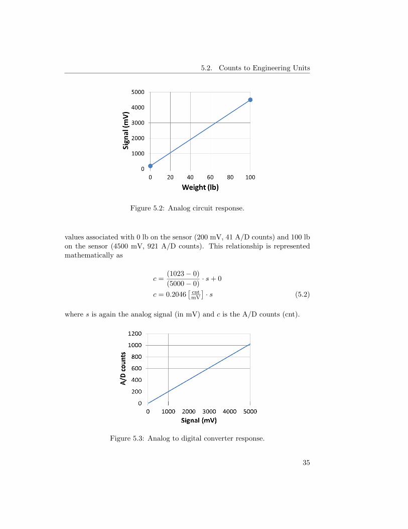
5.2. Counts to Engineering Units
Figure 5.2: Analog circuit response.
values associated with 0 lb on the sensor (200 mV, 41 A/D counts) and 100 lbon the sensor (4500 mV, 921 A/D counts). This relationship is representedmathematically as
c =(1023− 0)
(5000− 0)· s+ 0
c = 0.2046[cntmV
]· s (5.2)
where s is again the analog signal (in mV) and c is the A/D counts (cnt).
Figure 5.3: Analog to digital converter response.
35

5. Analog Input
Table 5.1: Parameters for analogReference().
Parameter Analog Reference Voltage
DEFAULT 5 VINTERNAL 1.1 VEXTERNAL AREF pin value
Note: These values are for the Arduino Uno and vary for other platforms.
The complete response can now be represented mathematically by substi-tuting Equation (5.1) into Equation (5.2).
c = 0.2046 · sc = 0.2046 · (43 · w + 200)
c = 8.7978[cntlb
]· w + 40.92 [cnt] (5.3)
While the above equation describes the A/D counts that will result for agiven weight, we are actually interested in the opposite direction. The softwarewould like to know the weight, and what it has are counts. We can get thatby simply inverting Equation (5.3).
w = 0.1136648[
lbcnt
]· c− 4.6512 [lb] (5.4)
This gives weight (in lbs) given A/D counts.
The above example makes the implicit assumption that the range of A/Dcounts (which is 0 to 1023) happens over an input voltage range of 0 to 5 V.This is not always the case. The top end of the voltage range (that correspondsto 1023 A/D counts) is adjustable. We will see how to do this in the followingsection.
5.3 Software
Figure 5.4 shows a sketch that utilizes the analog input hardware described inthe previous section. The scale of the analog range is set using analogReference().With the parameter DEFAULT, the analog input range is configured to be 0 to5 V. Table 5.1 shows other possible settings.
The loop() code reads the analog input value, converts the value intoengineering units (lbs in this case) using Equation (5.4), and prints both theA/D counts and the weight.
36

5.4. Example Analog Input Use Cases
const int aiPin = 14; // analog input A0 is pin 14
int rawValue = 0; // raw input value
float weight = 0.0; // weight in lbs
void setup() {
analogReference(DEFAULT); // set analog range
Serial.begin(9600);
}
void loop() {
// read the input
rawValue = analogRead(aiPin);
// compute weight
weight = (float)(0.1136648 * rawValue - 4.6512);
// print results
Serial.print("Raw value = ");
Serial.print(rawValue);
Serial.print(" Weight = ");
Serial.print(weight);
Serial.println(" lbs");
}
Figure 5.4: Example analog input sketch.
5.4 Example Analog Input Use Cases
In this section, we will illustrate the use of analog inputs for three differentpurposes. To illustrate a variety circumstances, each use case will have someunique property built into the example.
5.4.1 Temperature
This first example illustrates the use of a different reference voltage, which isset using the analogReference() call.
Consider a temperature probe that generates an output voltage with thefollowing parameters: 10 mV/◦C voltage change with temperature and 0 V at0 ◦C. We are interested in measuring liquid water, so the range of temperatureswe need to consider are 0 to 100 ◦C. The above lets us construct an equation
37

5. Analog Input
for the voltage response of the probe as follows:
s = 10[mV◦C
]· t (5.5)
where s is the analog voltage signal into the A/D converter and t is thetemperature in ◦C.
If we use INTERNAL as the parameter to analogReference(), the top ofthe voltage range is 1.1 V, which will be just above the highest temperaturewe wish to read (1000 mV at 100 ◦C). The conversion from analog voltage toA/D counts is therefore
c =(1023− 0)
(1100− 0)· s (5.6)
c = 0.93[cntmV
]· s (5.7)
which gives
c = 0.93 · (10 · t) (5.8)
c = 9.3[cnt◦C
]· t (5.9)
as the expression for A/D counts given temperature, and
t = 0.1075[ ◦Ccnt
]· c (5.10)
as the expression for temperature given A/D counts. The code to convertA/D counts into engineering units (temperature in ◦C) is therefore
temp = (float) (0.1075 * rawValue);
where temp is a float representing temperature and rawValue is an int thathas the raw A/D count value.
5.4.2 Level
This second example shows an analog input in which the increasing signalgoes the opposite direction. Consider the liquid level sensor of Figure 5.5. Inthis example the height of the liquid vessel is 4 cm, and the top of the sensoris 5 cm above the bottom of the vessel. The sensor circuit’s voltage responseis 1 V/cm, measured from the top of sensor to the level of the liquid in thevessel.
As a result of this mode of operation, the circuit will read 5 V (5000 mV)when the vessel is empty and 1 V (1000 mV) when the vessel is full. We are
38

5.4. Example Analog Input Use Cases
Figure 5.5: Liquid level measurement.
interested in knowing the level of the liquid in the vessel. We can express thevoltage signal, s, as a function of liquid level, L, as follows.
s =(1000− 5000)
(4− 0)· L+ 5000 (5.11)
s = −1000[mVcm
]· L+ 5000 [mV] (5.12)
using the points (0 cm, 5000 mV) and (4 cm, 1000 mV) to define the linearresponse. Returning to a 5 V reference, this equation gets substituted intoEquation (5.2) to yield
c = 0.2046 · (−1000L+ 5000) (5.13)
c = −204.6[cntcm
]· L+ 1023 [cnt] (5.14)
as the expression for A/D counts given level, and
L = −0.0048876[cmcnt
]· c+ 5 [cm] (5.15)
as the expression for level given A/D counts. The code to convert A/D countsinto engineering units (level in cm) is therefore
level = (float)(-0.004876 * rawValue + 5);
where level is a float representing the liquid level in cm.Note that this analog reading really does work the same as the previous two
examples (sensing weight and temperature), with the only distinction beingthat the slope of the response curve is negative. Therefore, the A/D countsgo down as the liquid level goes up.
39

5. Analog Input
5.4.3 Acceleration
In addition to using the internal A/D converter, it is often the case that weinterface a microcontroller to other subsystems that have been optimized fora particular purpose. In the microcontroller world, we frequently use whatis known as the I2C bus to connect the microcontroller to peripheral devices,such as sensors and actuators.
As an example, the MMA8451Q is an integrated circuit (manufacturedby Freescale) that functions as an accelerometer. The block-level diagramand directional reference are shown in Figure 5.6, which are reproductions ofFigures 1 and 2 of the part’s data sheet.
Figure 5.6: Block diagram and directional reference for Freescale MMA8451Qaccelerometer(from the data sheet).
40

5.4. Example Analog Input Use Cases
Observe that the part is actually noticeably more complex than our Ar-duino processor. It has a built-in processor of its own (that performs the“embedded DSP functions” on the block diagram), in addition to three trans-ducers (oriented along each axis), analog-to-digital conversion, and varioussupport functions.
The A/D converter that is built in to the accelerometer is 14 bits, so thevalues range from 0 to 8191 (0 to 214 − 1). In addition, the processor thatis built in to the accelerometer will perform the scale conversions, return-ing acceleration in m/s2. In either case, we access the information from theaccelerometer using libraries provided by the manufacturer.
41


6 Timing
There are lots of ways to reason about the passage of time in computer systems,generally. At one end of the spectrum, how much time a program takes toexecute is only an issue if it becomes long enough to be distracting to theuser. For example, if the task of a program is to add the value of someonesassets and subtract the value of his/her debts to determine net worth, until theprogram takes longer to run than it takes the human to enter the program’sinputs and observe the program’s outputs, how long it takes to run is almostirrelevant. As a user, what do I care if it completes in 1 millisecond or in10 milliseconds? TV screens take more than 30 milliseconds to update eachframe, and to our human eyes that looks like smooth and continuous motion.
If the amount of time that a program takes to execute is primarily a matterof convenience for the user, we refer to the execution time as a non-functionalproperty of the program (i.e., it is not part of the function that the program isexpected to perform). Another way to say this is that how long the programtakes to run is not formally part of the correctness criteria of the program. Itis judged to be providing a correct answer even if it takes a long time to getto that answer.
At the other end of the spectrum, there are computer programs for whichwhen they provide a result is just as important as the value that they provide.Consider a computer program that is managing the flight control surfaces ona high-performance aircraft. If the program tells the aileron to move up (e.g.,because the pilot has moved the control stick), but provides that output toolate, the aircraft can crash. This is a much more serious result than simplyuser inconvenience.
When time is an explicit component in the correctness criteria (i.e., timeis a functional property), we refer to it as a real-time program. Real-timeprograms are often divided into two classes. The first, called hard real-time,are those for which serious dire consequences will result if some timing deadlineis missed. This would be the case for our aircraft control example above.The second, called soft real-time, are those for which there is some degree
43

6. Timing
of slack, or forgiveness, in the timing requirements. A good example hereis video playback. If you are watching a video and one or two individualframes are missing, you will never perceive it and the playback experience willbe a positive one (at approximately 30 frames per second, you’ll never missit). It is not until lots of frames are missing (or delayed) that you will startcomplaining about the viewing experience. Here, timeliness is clearly partof the correctness criteria for the playback software. However, occasionallymissing a few of the timing specifications isn’t a life-and-death matter.
For computer systems that interact with the physical world, it is quitecommon for timing to be an important part of the functional properties ofthe programs we run. Sometimes they might be hard real-time specifications,other times they might be soft real-time requirements. Most of the time,however, they will include time in some way.
6.1 Execution Time
Any computer program takes time to execute. As described in Chapter 10, itis physically possible to count the individual instructions that the computerexecutes, and if you know how much time each instruction takes, it is possibleto know (with surprisingly good precision) how long a computer takes toexecute a specific instruction sequence.
There are two major problems with this approach in practice. First, inmany cases we do not know ahead of time how many instructions will execute.As soon as there is a conditional branch in our program (e.g., an if...then
statement or a while loop) for which the condition is dependent upon someinput value, then different runs of the program will have different numbers ofinstructions to execute.
Second, only on the simplest processors do we actually know how muchtime each instruction takes to execute. On modern processors, there are awhole host of reasons why each instruction can take more or less time toexecute. Variations in memory access time, execution pipeline bubbles, out-of-order execution, and contention for needed resources are but a few of thecauses that limit our ability to know how much time each instruction takesbefore it is complete.
As a result, counting of instructions is only very rarely used as an effectivemechanism for managing time within programs. In virtually all processors,from the most advanced multicore to the simplest microcontroller, there arededicated circuits that are tasked with the job of measuring the passage oftime. A simple example is a free-running counter that is incrementing at a
44

6.2. Controlling Time
given frequency. If the counter updates at 1 MHz, each microsecond (µs) thecounter value increases by 1. (If f is the frequency, 1 MHz or 1,000,000 Hzin this case, and T is the period, then T = 1/f = 1 µs.) The pseudocodein Figure 6.1 then enables the program to know how much time has elapsedbetween two different points in the code (e.g., before and after a section ofcode we want to know how long it takes to execute).
startTime = readFreeRunningCounter()
// execute timed code
endTime = readFreeRunningCounter()
runTime = endTime - startTime
Figure 6.1: Measuring elapsed time with a free-running counter. The vari-able runTime indicates the execution time of the timed code, in time unitsdependent upon the free-running counter’s frequency.
In the Arduino C environment, there are two functions that are available toaccess the free-running counter on the microcontroller. The first, millis(),returns the number of milliseconds since the last processor reset, and thesecond, micros(), returns the number of microseconds since the last processorreset. Both functions return a long int type since an int will quickly runout of space to store sufficiently large values (see Chapter 8).
6.2 Controlling Time
The discussion above enables us to measure the elapsed time of a section ofcode; however, frequently the task is to ensure that actions in a program takea specific amount of time, or happen at a given rate. A simple example isthe flashing LED of Chapter 2, the code for which is repeated in Figure 6.2.This sketch does a reasonable job flashing the LED at 1 Hz. The delay() calltakes one argument, the number of milliseconds to delay, and returns from thecall approximately that many milliseconds later. We’ve used this techniqueseveral times already, not only in Chapter 2.
There are a pair of (related) limitations to this method of managing timewithin a program. The first limitation is that this loop will not really run at1 Hz. Invariably, it will run somewhat slower than 1 Hz (i.e., the total time toexecute the loop will be something more than 1 second). This is because thereare instructions to be executed in the loop that are outside of the delay() call,and those instructions take time to execute. Both calls to digitalWrite()
45

6. Timing
const int doPin = 17; // digital output pin is 17
void setup() {
pinMode(doPin, OUTPUT); // set pin to digital output
}
void loop() {
digitalWrite(doPin, HIGH); // set the output HIGH
delay(500); // wait for 0.5 s (500 ms)
digitalWrite(doPin, LOW); // set the output LOW
delay(500); // wait for 0.5 s
}
Figure 6.2: Simple timing loop.
are outside of delay(), and there is some non-zero overhead associated withthe loop() construct as well.
The second limitation is that the 1 second loop time will grow any timeadditional functionality is added to the loop. Consider the addition of a singleline of code,
Serial.println(millis());
which will print the current value of the free-running counter. By observingthe sequence of counter values printed, we can then discern actually how longit takes to execute the loop. Since this new code takes additional time toexecute, the amount of time spent in the loop has now been altered. Notonly is it never going to be precisely 1 second, the amount that it grows from1 second is dependent upon things like adding diagnostic statements.
Note that the timing errors that result from extra code execution accu-mulate from one loop to the next. Once we get behind, we never catch backup. We only get further and further behind. There is, of course, a better wayto do this, and the next section describes a technique for controlling time insoftware that is dramatically more robust. It doesn’t fix everything, but itworks considerably better than the methods described above.
46

6.3. Delta Time
6.3 Delta Time
The use of the delay() routine to control time has the issues described above,that all the code that is outside the delay() call isn’t accounted for in theelapsed time for the loop. We will next examine a more robust timing ap-proach, called delta time, that avoids some (but not all) of these issues.
Like the example above, we will assume that the task at hand is to executethe loop once per second. We will simplify the task by no longer havingmultiple timed events within the loop, but only concern ourselves with thetotal loop time. The code to implement the delta time approach is shown inFigure 6.3.
const long deltaTime = 1000; // loop period (in ms)
long loopEndTime = deltaTime;
void setup() {
}
void loop() {
if (millis() >= loopEndTime) { // one period is complete
loopEndTime += deltaTime;
// code to be executed once per iteration
}
}
Figure 6.3: 1 Hz timing loop using delta time techniques.
Consider how this timing approach works. We maintain a variable thatindicates when the next 1 s period will be complete, loopEndTime. When thefree-running counter has exceeded this value, we know that our loop periodhas elapsed. When this happens, we update the end-of-loop time and proceedto run the code that should execute once per loop.
This is different than the delay() based approach above in several ways.First, as long as the code that is executed once per loop (call it an iteration)doesn’t take longer than 1 s to run, the code within the if condition will faith-fully execute once per second. This is true whether the “once per iteration”code takes 1 microsecond, 10 milliseconds, or 900 milliseconds. As long as itis less than 1 second, the timing is preserved.
Second, even an occasional excursion beyond 1 s by the “once per iteration”code doesn’t necessarily have dire consequences. While the next iteration will
47

6. Timing
be delayed (by the amount the previous iteration was late in finishing), thelogic of updating the loopEndTime by deltaTime each iteration ensures thatsubsequent iterations will revert to the once per second intended rate. Thisis reasonable operation for many soft real-time tasks (although it is certainlynot sufficiently robust for hard real-time operation).
The approach of Figure 6.3 is not the only possible design for delta timing.There are a number of possible designs, each with slightly different properties(primarily of what happens when the timing isn’t perfect, or an iteration islate). For example, in Figure 6.3, if an individual iteration is late, the nextiteration will be back on the original schedule (i.e., 2 s after the start of thelate iteration). Sometimes that isn’t what we want to happen. Figure 6.4illustrates an alternative design that has slightly different properties when aniteration is late. It also introduces another common convention, which is thatwe make a call to millis() once per loop, retaining the result of the call, andthen use that value throughout the loop. This ensures that “time” (i.e., thesoftware’s concept of what time it is) doesn’t change in the middle of loop().
const long deltaTime = 1000; // loop period (in ms)
long loopEndTime = deltaTime;
long currentTime = 0;
void setup() {
}
void loop() {
currentTime = millis();
if (currentTime >= loopEndTime) { // one period is complete
loopEndTime = currentTime + deltaTime;
// code to be executed once per iteration
}
}
Figure 6.4: Alternative 1 Hz timing loop using delta time techniques.
In this sketch, if an iteration is late, the 1 s time period restarts at thebeginning of the next iteration. This is because we’ve added deltaTime notto the scheduled loopEndTime, but instead to the currentTime, which mightbe later than loopEndTime. I.e., the 1 s period restarts rather than tries tocatch up.
48
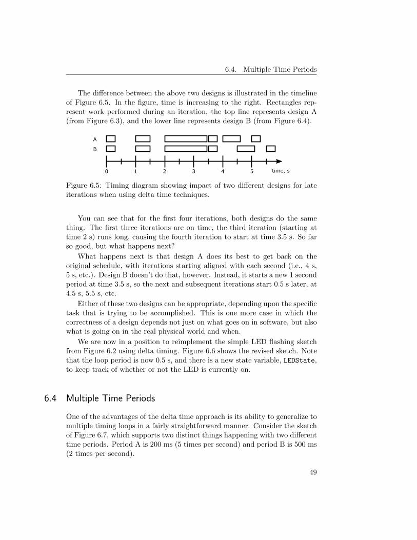
6.4. Multiple Time Periods
The difference between the above two designs is illustrated in the timelineof Figure 6.5. In the figure, time is increasing to the right. Rectangles rep-resent work performed during an iteration, the top line represents design A(from Figure 6.3), and the lower line represents design B (from Figure 6.4).
Figure 6.5: Timing diagram showing impact of two different designs for lateiterations when using delta time techniques.
You can see that for the first four iterations, both designs do the samething. The first three iterations are on time, the third iteration (starting attime 2 s) runs long, causing the fourth iteration to start at time 3.5 s. So farso good, but what happens next?
What happens next is that design A does its best to get back on theoriginal schedule, with iterations starting aligned with each second (i.e., 4 s,5 s, etc.). Design B doesn’t do that, however. Instead, it starts a new 1 secondperiod at time 3.5 s, so the next and subsequent iterations start 0.5 s later, at4.5 s, 5.5 s, etc.
Either of these two designs can be appropriate, depending upon the specifictask that is trying to be accomplished. This is one more case in which thecorrectness of a design depends not just on what goes on in software, but alsowhat is going on in the real physical world and when.
We are now in a position to reimplement the simple LED flashing sketchfrom Figure 6.2 using delta timing. Figure 6.6 shows the revised sketch. Notethat the loop period is now 0.5 s, and there is a new state variable, LEDState,to keep track of whether or not the LED is currently on.
6.4 Multiple Time Periods
One of the advantages of the delta time approach is its ability to generalize tomultiple timing loops in a fairly straightforward manner. Consider the sketchof Figure 6.7, which supports two distinct things happening with two differenttime periods. Period A is 200 ms (5 times per second) and period B is 500 ms(2 times per second).
49

6. Timing
const int doPin = 17; // digital output pin is 17
int LEDState = LOW; // current LED output value
const long deltaTime = 500; // loop period (in ms)
long loopEndTime = deltaTime;
void setup() {
pinMode(doPin, OUTPUT); // set pin to digital output
digitalWrite(doPin, LEDState);
}
void loop() {
if (millis() >= loopEndTime) { // one period is complete
loopEndTime += deltaTime;
LEDState = !LEDState; // toggle LED state
digitalWrite(doPin, LEDState);
}
}
Figure 6.6: LED flash using delta timing techniques.
Notice that there isn’t anything resembling a free lunch here. If both loopstrigger at the same time (which they will in this example once per second),the code for the 500 ms period will execute after the code for the 200 msperiod. If the code for the 200 ms period takes a significant length of time,the 500 ms code will be late. Whether or not this is a problem will, of course,depend on the overall properties of the system.
50

6.4. Multiple Time Periods
const long deltaTimeA = 200; // loop period A (in ms)
const long deltaTimeB = 500; // loop period B (in ms)
long loopEndTimeA = deltaTimeA;
long loopEndTimeB = deltaTimeB;
long currentTime = 0;
void setup() {
}
void loop() {
currentTime = millis();
if (currentTime >= loopEndTimeA) { // period A is complete
loopEndTimeA += deltaTimeA;
// code to be executed once per 200 ms
}
if (currentTime >= loopEndTimeB) { // period B is complete
loopEndTimeB += deltaTimeB;
// code to be executed once per 500 ms
}
}
Figure 6.7: Two timing loops using delta time techniques.
51

7 Design Patterns
While we have been discussing design throughout the book, it is worth notingthat one of the ways that we can implement good designs is to follow the leadof good designers that preceded us. Artists of every form, from musiciansto painters, like to give credit to those who preceded them and providedinspiration, guidance, and examples to follow. As designers of computingsystems, we shouldn’t be any different. In this chapter, we will introducesome design patterns that are worthwhile to emulate.
7.1 Finite-State Machines
One of the design patterns that sees quite a bit of use is a finite-state ma-chine (FSM), also called a finite-state automaton. An FSM is a computationalabstraction in which things in the machine to be remembered are representedby individual states, and there are a finite number of states (hence the name).
The FSM abstraction can be quite useful, helping to keep a design man-ageable and straightforward to reason about. We will introduce the conceptof a finite-state machine with a simple example. Consider the operation of asuper-simple vending machine. There is only one thing for sale, and it costs20¢. The vending machine can only accept nickels and dimes (no pennies,quarters, half-dollars, dollar coins, or bills). Also, it doesn’t provide change(see, we said it was super simple, we weren’t kidding).
A finite-state machine diagram that describes the operation of our vendingmachine is shown in Figure 7.1. It has 4 states, which are represented in thediagram as circles. Sometimes, this type of finite-state machine diagram iscalled a bubble diagram, with the circles representing individual states beingcalled state bubbles. The table below the diagram gives the meaning associatedwith each state. In our case, the vending machine needs to remember howmuch money has been deposited so far (i.e., what is the accumulated value).One state (in our case, the “0¢” state in the upper left of the diagram) is
53

7. Design Patterns
identified as the initial state, which is where the finite-state machine starts.
State Meaning
0¢ $0.00 accumulated value (initial state)5¢ $0.05 accumulated value10¢ $0.10 accumulated value15¢ $0.15 accumulated value
Figure 7.1: Vending machine finite-state diagram.
When someone who is trying to buy the item for sale inserts an individualcoin, the operation of the FSM is indicated by the directed edges (arcs witharrowheads) that are labeled with the possible inputs. In this case, the possibleinputs are two kinds of coin: (1) a nickel (shown as the label “5¢”) or (2) adime (shown as the label “10¢”).
Note that the abstraction only supports one input at a time. When theinput arrives (coin is deposited), the FSM follows the edge indicated by theappropriate label, ending up in a new state. From the initial state, “0¢”, ifour customer inserts a nickel, the FSM moves to the state “5¢”. Alternatively,if our customer inserts a dime, the FSM moves to the state “10¢”.
Now, in a new state, the FSM is ready to receive another coin. If, forexample, the first coin was a nickel and we are now in the state “5¢”, if thenext coin is another nickel, we will go to the state “10¢”, and if the next coinis a dime, we will go to the state “15¢”.
There is an important principle worth noting at this point. If the firstcoin was a dime, the FSM ended up in the state “10¢”, and if the first andsecond coins were both nickels, the FSM also ended up in the state “10¢”. Thememory of how the FSM got to the state “10¢” is not retained, however. The
54

7.1. Finite-State Machines
FSM only “remembers” that the accumulated value to this point is 10 cents,not whether it came in the form of a dime or two nickels.
If we are in the state “10¢” and the next coin is a dime, the customerhas provided enough money to buy what we are selling, so the transactioncan be completed (e.g., the vending machine can deliver the item), and theFSM can return to the state “0¢” so as to be ready for the next sale. In thediagram, we are only showing the state transition(s) to state “0¢”, not thesales. However, it is possible to show that kind of information on a finite-statemachine diagram as well (and we will do so in a later example).
As described so far, the finite-state machine is just a computational ab-straction. We can implement the finite-state machine in multiple ways. Justlike we did in Chapter 3, where we were able to implement the logic for test-ing the economics requirement either in hardware or in software, we have thesame options available to us for implementing finite-state machines. Whetherconstructed using hardware or software, the same computational abstractionis used.
Here, we will stick with a software implementation, which is shown inFigure 7.2. The state of the FSM is retained in a variable, FSMstate, whichcan have one of the following values:
STATE_0_CENTS STATE_5_CENTS STATE_10_CENTS STATE_15_CENTS
and has initial value STATE 0 CENTS. There are several design choices for howto do this, but we will illustrate it with the use of an enumeration.
enum state {
STATE_0_CENTS,STATE_5_CENTS,STATE_10_CENTS,STATE_15_CENTS}
};
state FSMstate = STATE_0_CENTS;
In the code provided in the figure, the routine vend() is invoked when anitem has been sold. The loop executes the logic of the FSM. It first receivesa coin, into inputCoin, and then decides what to do (what is the next state,and whether or not a sale has been completed ) based on the current stateand the value of the coin.
In this example, a switch statement is used to separate the logic for eachstate (one case per state), and if statements are used to distinguish differentinput coins. However, there is no requirement that it be implemented thisway. We could have used switch statements for both state and input, forexample.
55

7. Design Patterns
void loop () {
inputCoin = inputNextCoin();
switch (FSMstate) { // code to implement FSM
case STATE_0_CENTS:
if (inputCoin == NICKEL) {
nextFSMstate = STATE_5_CENTS;
}
if (inputCoin == DIME) {
nextFSMstate = STATE_10_CENTS;
}
break;
case STATE_5_CENTS:
if (inputCoin == NICKEL) {
nextFSMstate = STATE_10_CENTS;
}
if (inputCoin == DIME) {
nextFSMstate = STATE_15_CENTS;
}
break;
case STATE_10_CENTS:
if (inputCoin == NICKEL) {
nextFSMstate = STATE_15_CENTS;
}
if (inputCoin == DIME) {
nextFSMstate = STATE_0_CENTS;
vend();
}
break;
case STATE_15_CENTS:
nextFSMstate = STATE_0_CENTS;
vend();
break;
}
FSMstate = nextFSMstate;
}
Figure 7.2: Source code for vending machine FSM controller.
56

7.1. Finite-State Machines
At the bottom of the loop, the current state, FSMstate is updated to takeon the value of the next state, nextFSMstate, and the loop repeats.
While the code in Figure 7.2 faithfully represents the functionality rep-resented by the FSM diagram in Figure 7.1, notice how much easier it is tofollow what is going on in the diagram (as opposed to the code). The abstractrepresentation of the diagram is much clearer, less error-prone, and definitelythe preferred way to communicate the operation of the vending machine tohumans.
For example, what if we wanted to make a small change to the way thevending machine operates. Our current design doesn’t support the return ofchange to the customer. For example, if we are in state “15¢” and the customerinserts a dime, the sale is made (and the FSM returns to state “0¢”), but thefact that the customer actually provided 25 cents is ignored.
In our alternative vending machine, shown in Figure 7.3, if the customerprovides 25 cents, the 5 cents in change is made available to the next customer(OK, this really is pretty silly, but we are just illustrating a point here). Inthe FSM diagram, this is accomplished by simply adding one more edge (fromthe state “15¢” to the state “5¢”) and changing the appropriate labels on theedges outbound from the state “15¢”.
State Meaning
0¢ $0.00 accumulated value (initial state)5¢ $0.05 accumulated value10¢ $0.10 accumulated value15¢ $0.15 accumulated value
Figure 7.3: Alternative vending machine finite-state diagram.
Notice how by using an appropriate computational abstraction, a finite-
57

7. Design Patterns
state machine, simple changes to the functionality of the vending machinecan be communicated with simple changes to the FSM diagram. In the nextexample, we will expand the notion of the FSM computational abstraction toinclude output functionality as well (which was in the code for our vendingmachine example, but wasn’t shown on the FSM diagram).
One of the things that finite-state machines are really good at is decidingwhether or not a sequence of input symbols (i.e., characters) match a specifiedpattern. Take, for example, a Social Security Number (SSN). It typically iswritten in the following form:
xxx-xx-xxxx
where each x in the above notation represents a decimal digit between 0 and9. The diagram of Figure 7.4 illustrates an FSM that recognizes streams ofinput characters when they match this pattern.
The states in this FSM are labeled A through K, and the meaning of eachstate is provided in the table below the diagram in the figure. The initial stateis A. The are several important things different about this FSM diagram ascompared to the diagrams we have seen so far, and they all relate to the labelson the edges. First, we have introduced a shorthand notation for indicating arange of characters. Take a look at the label on the edge from state A to stateB. We wish to move from A to B for any character in the range 0 to 9, and thisis indicated in the diagram with the notation [0-9].
Second, for any character not in the range 0 to 9, we want to follow theother edge (which is a self-loop back to A). This is denoted by the - symbol(right before the /, which we’ll address next). The - symbol can be interpretedto mean “an input not specified on some other outgoing edge from this state.”
Third, for this self-loop edge (from A to A), after the input designation of- there is a / followed by the note err. The notation after the / indicatesan output of the finite state machine. In this case, we are indicating thanan error has occurred (i.e., the input sequence is not in the form of an SSN).Notice that when in state K, both outbound edges return to state A, and whatdistinguishes these two edges is whether or not we have an error (the edgewith label -/err) or we have successfully recognized an SSN (the edge withlabel [0-9]/accept). Edges without a / don’t generate any output when theedge is traversed by the FSM implementation.
Fourth, given that the - symbol represents “anything else” as an inputcharacter, when we are explicitly expecting a hyphen (e.g., when in state D)we denote that input symbol by putting it in quotes (i.e., "-").
Fifth, while the / is used pretty universally to separate input symbols fromoutput actions in finite-state machine diagrams, we pretty much made up the
58

7.1. Finite-State Machines
State Meaning
A Waiting for digit no. 1 (initial state)B Received 1st digit, waiting for digit no. 2C Received 2nd digit, waiting for digit no. 3D Received 3rd digit, waiting for dash no. 1E Received 3 digits and 1st dash, waiting for digit no. 4F Received 4th digit, waiting for digit no. 5G Received 5th digit, waiting for dash no. 2H Received 5 digits and 2 dashes, waiting for digit no. 6I Received 6th digit, waiting for digit no. 7J Received 7th digit, waiting for digit no. 8K Received 8th digit, waiting for digit no. 9
Figure 7.4: SSN finite-state machine diagram.
rest of the notation. Some designate ranges with a colon (e.g., 0:9 ratherthan 0-9) and don’t always include the square brackets. Others designate the“anything else” input by simply not indicating an input (i.e., leaving it blank).The important point here is to remember that the FSM diagram is intendedto be read by humans, so as long as the reader has been informed of theconventions in use, he/she should be able to interpret the diagram correctly.
As we did for our first vending machine example, we will also show howthe SSN recognizer FSM can be implemented in software. The code is shownin Figures 7.5 and 7.6. As in the earlier example, the current state of the FSMis retained in the variable FSMstate, which can only have the values A throughK (as defined by either a set of #define statements or const int declarationsearlier). The boolean functions isNumber() and isDash() determine whetheror not the provided character matches the appropriate condition. The outputs
59

7. Design Patterns
are implemented in the routines error() and accept(). Both the boolean
functions and output routines need to be provided elsewhere in the sketch(e.g., the function isNumber() is available as the library routine isDigit()).
In the earlier example we made the point that the diagram was muchsimpler to follow than the code. While that is certainly still the case, thereis an additional point to be made here. Note that the 11-state finite-statemachine diagram fit in substantially less than a page, while the code consumedtwo full pages, and technically only includes the details for 6 of the 11 states.
7.2 Polling and Interrupts
In this section, we will talk about a pair of design patterns that are bothquite prevalent in microcontroller systems and overlap to some degree in whatthey can accomplish. While they can be used for a variety of purposes, wewill focus on their use in reading and interpreting input signals that originateexternal to the processor (mostly digital inputs).
7.2.1 Polling
Polling an input signal refers to the repeated, periodic reading of that signal.Figure 7.7 illustrates a simple example of polling a digital input pin (adaptedfrom Figure 3.2), in which each loop() the digital input pin is read, the valueretained in diValue, and various actions happen depending upon the currentand previous digital input values.
One of the salient features of this design pattern is that the input is readonly once per iteration. Throughout the rest of the iteration, when the logicdepends upon the current input value it takes it from the variable diValue. Inthis way, we are assured that the “logical” value of the input doesn’t changepart way through the iteration (e.g., the if test passes and then the printstatement shows the input as LOW).
This property is important if we are trying to perform logic as shown inthe sketch. At the end of each iteration, the current diValue is saved inprevValue, so during the following iteration, prevValue retains the previousvalue of the digital input. In this way, testing for the previous value being LOW
and the current value begin HIGH lets us reliably determine in which iterationdoes the input transition from low to high.
In this example sketch, when the low-to-high input transition is detected,the digital output is sent HIGH for 200 ms. Because we used a call to delay()
to implement the 200 ms wait, the length of time required for each iterationvaries. In many circumstances, polling an input with a variable period is
60

7.2. Polling and Interrupts
void loop () {
char inputSymbol = inputNextCharacter();
switch (FSMstate) { // code to implement FSM
case A:
if (isNumber(inputSymbol)) {
nextFSMstate = B;
}
else {
nextFSMstate = A;
error();
}
break;
case B:
if (isNumber(inputSymbol)) {
nextFSMstate = C;
}
else {
nextFSMstate = A;
error();
}
break;
case C:
...
case D:
if (isDash(inputSymbol)) {
nextFSMstate = E;
}
else {
nextFSMstate = A;
error();
}
break;
case E:
...
Figure 7.5: Source code for SSN finite-state machine. (Continued, next page.)
61
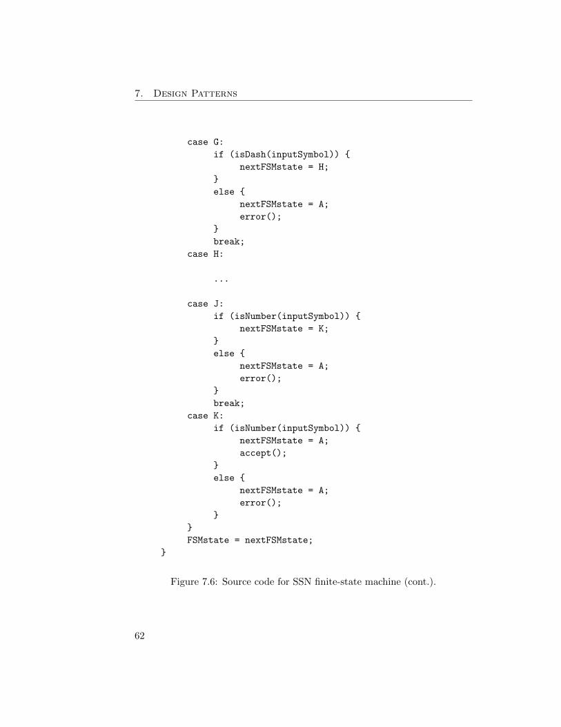
7. Design Patterns
case G:
if (isDash(inputSymbol)) {
nextFSMstate = H;
}
else {
nextFSMstate = A;
error();
}
break;
case H:
...
case J:
if (isNumber(inputSymbol)) {
nextFSMstate = K;
}
else {
nextFSMstate = A;
error();
}
break;
case K:
if (isNumber(inputSymbol)) {
nextFSMstate = A;
accept();
}
else {
nextFSMstate = A;
error();
}
}
FSMstate = nextFSMstate;
}
Figure 7.6: Source code for SSN finite-state machine (cont.).
62

7.2. Polling and Interrupts
const int diPin = 16; // digital input pin is 16
const int doPin = 17; // digital output pin is 17
int diValue = LOW; // digital input value
int prevValue = LOW; // previous input value
void setup() {
pinMode(diPin, INPUT); // set pin to digital input
pinMode(doPin, OUTPUT); // set pin to digital output
digitalWrite(doPin, LOW);
Serial.begin(9600);
}
void loop() {
diValue = digitalRead(diPin); // read the input
if (prevValue == LOW && diValue == HIGH) {
digitalWrite(doPin, HIGH);
delay(200);
digitalWrite(doPin, LOW);
}
Serial.print("input value = ");
Serial.println(diValue);
prevValue = diValue;
}
Figure 7.7: Polling example sketch.
not a good choice (e.g., when we are reading an analog input value and wewant samples at regular time intervals). In these cases, we can use deltatiming techniques to both: (a) regularize the time period of each iteration,and (b) implement the 200 ms pulse for the digital output signal.
Figure 7.8 illustrates the use of delta timing to accomplish the goals statedabove. In this sketch, five iterations happen each second (200 ms per itera-tion), and the digital input is read precisely once per iteration. When theoutput signal goes HIGH, due to the low-to-high transition on the input, it issent LOW one iteration later.
But what happens in the sketch of Figure 7.8 if the digital input signalgoes high for 100 ms and then goes back low? Since the digital input is beingpolled every 200 ms, there is a significant chance that the high pulse that is
63

7. Design Patterns
const long deltaTime = 200; // loop period (in ms)
long loopEndTime = deltaTime;
long currentTime = 0;
const int diPin = 16; // digital input pin is 16
const int doPin = 17; // digital output pin is 17
int diValue = LOW; // digital input value
int prevValue = LOW; // previous input value
void setup() {
pinMode(diPin, INPUT); // set pin to digital input
pinMode(doPin, OUTPUT); // set pin to digital output
digitalWrite(doPin, LOW);
Serial.begin(9600);
}
void loop() {
currentTime = millis();
if (currentTime >= loopEndTime) { // one period is complete
loopEndTime += deltaTime;
diValue = digitalRead(diPin); // read the input
digitalWrite(doPin, LOW);
if (prevValue == LOW && diValue == HIGH) {
digitalWrite(doPin, HIGH);
}
Serial.print("input value = ");
Serial.println(diValue);
prevValue = diValue;
}
}
Figure 7.8: Polling sketch with regular period.
present on the input pin will be completely missed by the software.
One solution to this issue is to poll the input at a higher rate. If we haveknowledge that the shortest pulse that will be present at the input is, say,100 ms, a period shorter than this minimum pulse duration will always seeany low-to-high transition.
Another solution is to use a hardware feature present in microcontrollers
64

7.2. Polling and Interrupts
that allows us to alter the program flow of control under certain specifiedcircumstances, including the change in value of a digital input pin. Thishardware feature is called an interrupt and will be our next subject.
7.2.2 Interrupts
An interrupt is a change in program control flow based upon an explicit triggerevent. Interrupts can be triggered by a wide variety of things, including bothinternal events (e.g., a timer) and external events (e.g., a digital input pin).Here, we will consider using interrupts to detect the low-to-high transition onan input pin.
There are a number of things that must be present to accomplish this.
1. A trigger must be unambiguously specified for the interrupt to occur(e.g., a level change on a particular digital input pin).
2. A routine must be authored that is the target of the control flow change(i.e., the code that gets called when the trigger occurs). This routine iscommonly called an interrupt service routine (ISR), since it “services”the interrupt when it occurs.
3. Because the ISR cannot have parameters or a return value, mechanismsmust be put in place for interaction between the main sketch and theISR. This is typically accomplished through the use of global variables.
4. Care must be taken when accessing these global variables, because in-terrupt triggers can happen at any time.
We specify an interrupt trigger using the attachInterrupt() library rou-tine. The parameters are an interrupt number (provided by a call to thelibrary function digitalPinToInterrupt()), the name of the ISR, and oneof the modes listed in Table 7.1.
Table 7.1: Interrupt trigger modes.
Mode Meaning
LOW trigger interrupt whenever pin is lowCHANGE trigger interrupt whenever pin changes valueRISING trigger interrupt whenever pin goes from low to highFALLING trigger interrupt whenever pin goes from high to low
65

7. Design Patterns
When authoring the interrupt service routine, there are a number of lim-itations that must be followed. As already stated, the ISR cannot have pa-rameters and does not return a function value. In addition, a number of thetiming library routines will not operate as you otherwise might expect withinan ISR, because they use interrupts themselves. This includes delay() andmillis(). Finally, since only one ISR can run at a time, and interrupts canbe triggered at any time, an ISR should be as short as possible.
When declaring global variables to use with an ISR, include the volatile
keyword. When accessing (reading or writing) those global variables, makesure that interrupts are turned off (using noInterrupts() and interrupts()).The code that is executed while interrupts are off is called a critical section,implying that it is critical that an interrupt not occur during the executionof this code. As with and ISR, a critical section should also be as short aspossible.
If the trigger for an interrupt occurs while the interrupts are turned off(i.e., while the sketch is in a critical section), the interrupt is pending and willtrigger once interrupts have been turned back on.
Figure 7.9 illustrates a sketch that uses interrupts to detect when a digitalinput pin goes from low to high. The ISR is called catchRisingEdge andis shown at the bottom of the sketch. Note that it is very short, taking aslittle time to execute as is reasonable. The interrupt trigger is on the risingedge of diPin, as specified in the invocation of attachInterrupts(). Notethat only a limited number of pins support interrupts. The variable flag isused to communicate between the ISR and the main loop() and it is declaredvolatile. When flag is accessed in loop() it is in a critical section (whichis also very short).
Because catchRisingEdge() gets invoked by the microcontroller’s hard-ware interrupt mechanisms, it can happen any time that interrupts are on(the sketch is not in a critical section). This means that even a very shortpulse on the digital input pin will cause the interrupt to trigger, the ISR tobe called, flag to be set true, and the rising edge not to be missed.
7.2.3 Discussion
While the descriptions of both polling and interrupts used the example ofreading a digital input pin, both design patterns are frequently used for othertasks as well (e.g., regular timing for digital outputs, analog inputs and out-puts, etc.). As a general rule, polling is a simpler approach and is thereforeless prone to errors in implementation, while interrupts can accomplish somethings a time scales that are not readily accessible to polling.
66

7.2. Polling and Interrupts
const long deltaTime = 200; // loop period (in ms)
long loopEndTime = deltaTime;
long currentTime = 0;
const int diPin = 2; // pin 2 supports interrupts
const int doPin = 17; // digital output pin is 17
volatile boolean flag = false; // input rising flag
void setup() {
pinMode(diPin, INPUT); // set pin to digital input
pinMode(doPin, OUTPUT); // set pin to digital output
digitalWrite(doPin, LOW);
attachInterrupt(digitalPinToInterrupt(diPin),
catchRisingEdge, RISING);
}
void loop() {
currentTime = millis();
if (currentTime >= loopEndTime) { // one period is complete
loopEndTime += deltaTime;
digitalWrite(doPin, LOW);
noInterrupts(); // enter critical section
if (flag) {
digitalWrite(doPin, HIGH);
flag = false;
}
interrupts(); // exit critical section
}
}
void catchRisingEdge() {
flag = true;
}
Figure 7.9: Reading input using interrupts.
67


8 Information Representation
This chapter will deal with how information is represented within a computer.We will start with numbers, followed by characters and strings, and finish upwith how we represent images.
8.1 Numbers
Numbers come in lots of forms. We can talk about the counting numbers,integers, reals, or complex numbers. Algebra allows us to represent relation-ships between numbers, and reason about those relationships. Here, we areinterested in the approaches used to represent numbers with a computer. Thisincludes how to store numbers as well as manipulate them mathematically.
8.1.1 Brief History of Number Systems
We will start with a brief history of number systems. Did you ever wonderhow the Romans wrote down the number zero? Think about it, I is one, II istwo, III is three, IV is four, etc. But how did they write down zero?
In what follows, we will constrain ourselves to using standard positionalnotation (i.e., the numerical value of a symbol depends upon its position).
Counting Numbers
One of the earliest uses of written numbers is to count things. This is knownto have occurred by the late fourth millennium B.C. in Mesopotamia, presentday Iraq [7], although it might have happened even earlier than that.
In the decimal system that we humans typically use these days1, the firstseveral counting numbers are:
1 2 3 4 5 6 7 8 9 10 11 12 13 14 15 16 17 18 19 20 ...
1This was not always the case, the Babylonians used base 60, which is how we ended upwith 60 seconds in a minute and 60 minutes in an hour.
69

8. Information Representation
which starts at 1 but continues infinitely far to the right.
The counting numbers are good at measuring how much stuff I have. Forexample, with just the counting numbers I can compare with my neighbor,and say, “I have 7 cows and 2 goats. How many do you have?” And myneighbor can reply in a meaningful way.
Getting just a bit more formal, we say that the counting numbers areclosed under addition and multiplication. What this means is that if we knowthat a is a some counting number and we know that b is also some countingnumber, without knowing the particular values of a or b we do know thata + b is a counting number and a × b is a counting number. To say that anumber system (such as the counting numbers) is closed over some operationis to say that performing the operation on numbers within the system resultsin a number that is also within the number system. In other words, addinga pair of counting numbers cannot give you a negative number or a fraction,the result will always be another counting number.
Zero: Natural Numbers
If I’ve just told my neighbor that I have 7 cows and 2 goats, and I’ve alsopolitely inquired about how many he has, how does he respond if he has nocows? He can certainly say something like, ”I do not have any cows. However,I do have 4 goats.” This reply, of course, answers the question, but doesn’thelp us reason about “no” cows in an algebraic system.
Brahmagupta, an Indian mathematician, addressed the above issue bydescribing the rules governing the use of the number 0, or zero, in A.D. 628 [3].By incorporating 0 into our number system, we now have the natural numbers,which include all the counting numbers and zero as well. This number systemis also known as the whole numbers. Like the counting numbers, the naturalnumbers are closed under addition and multiplication.
Returning to our question earlier, how did the Romans write down zero?They didn’t, literally, as a number. Instead, they used the word nulla mean-ing “nothing.” They might write Ego non habent ullam vaccas, which whentranslated from Latin means, “I do not have any cows.”
Negative Numbers: Integers
If I can count things, you can guess that commerce isn’t far behind. In ex-change for some thing I value, I might give my neighbor 3 chickens. I canreason about this just fine if I have 3 or more chickens to give, but whatabout when I promise my neighbor 3 chickens but the chicks haven’t hatched
70

8.1. Numbers
yet (i.e., I don’t have 3 chickens to give)? I can, of course, say, “I owe you3 chickens.” Here, I am using words that are outside the number systemto differentiate two distinct meanings for the phrase “3 chickens.” “I own3 chickens” means something very different than “I owe 3 chickens.”
However, maybe there is a better way. Let’s introduce the concept ofnegative numbers, which gives us the number system called the integers. Withnegative numbers, rather than using different words to talk about 3 chickens,I can use one number system to represent both concepts. “I owe 3 chickens”gets transformed into “I own −3 chickens.”
Getting back to formalism, the integers are closed under addition, multi-plication, and subtraction. Clearly, the notion of giving my neighbor some ofmy chickens (either present or future chickens) can be represented using sub-traction. Another way we make formal statements about number systems isto describe forms of algebraic equations that can be solved within the numbersystem. For example, if a is a constant integer, we can solve equations of theform
x+ a = 0 (8.1)
and know that the value of x that solves the equation will be an integer.
A quick note on the names of different numbers. With the advent of neg-ative numbers, the numbers that are not negative came to be called positive2
Humanity has started down a path in which many number systems are namedas opposites. That is, the name of the number system borrows opposite labelsfrom the natural language words used to name them.
Rational Numbers
As you can well imagine, the development of number systems was stronglydriven by the needs of commerce. People need to know how much of this orthat they own, buy, sell, or trade. They also die, and their children inherit.
If I lived in antiquity and owned 2 pigs, when I died tradition held that my2 pigs were divided among my 3 sons. (Sorry gals, enlightened thinking aboutequality of the sexes came much later than the notion of rational numbers.)Each of my sons now owns 2/3 of a pig, and we have expanded our numbersystem to explicitly include ratios between integers. This defines the rationalnumbers. Note that the label “rational” comes from the root “ratio,” not theother English meanings associated with the word rational, such as reasonableor logical.
2Although it is the matter of some debate whether or not 0 is included in the positivenumbers, we’ll ignore this bit of minutia.
71

8. Information Representation
More formally, rational numbers are closed under addition, multiplication,subtraction, and division. If a and b are constant rational numbers, we cansolve equations of the form
ax+ b = 0 (8.2)
as long as a 6= 0.
Irrational Numbers: Reals
Once folks figured out the rational numbers, they thought they had it all down.Other than this weird issue of not being able to divide by zero, they could dopretty much everything they thought they wanted to. Addition, subtraction,multiplication, and division were all available to them, and the number systemhandled it all.
Except....
Figure 8.1 was puzzling. Given a right triangle (the angle at the bottomleft is precisely 90◦), with adjacent edges each of length 1, how long is theopposite edge, or the hypotenuse? If a is the length of the bottom edge (a = 1in this case), b is the length of the left-most edge (b = 1 in this case), and xis the unknown length of the hypotenuse, the Pythagorean theorem tells us
a2 + b2 = x2 (8.3)
and if we substitute the known values for a and b (and do a little algebraicmanipulation), we get
x2 − 2 = 0 (8.4)
for which there are two solutions: x =√
2 and x = −√
2.
Figure 8.1: Right triangle. How long is the hypotenuse (the edge opposite theright angle)?
The problem is that for centuries mathematicians couldn’t find rationalsolutions to Equation (8.4), because neither solution can be expressed as aratio of two integers. In other words, the rational numbers are not closedunder the square root operation.
72

8.1. Numbers
The real numbers expand the number system beyond the rational numbersto include values that cannot be expressed as a ratio of two integers. Examplesinclude
√2 (illustrated above), π (the ratio of the circumference of a circle to
its diameter), and e (the base of the natural logarithms).Real numbers that are not rational numbers are called irrational numbers.
You might notice the pattern mentioned above continuing. In the naming ofnumber systems, numbers that are not rational are called irrational. However,remember that rational came from ratio, not the other possible meanings ofrational in English (e.g., logical, reasonable). As a result, irrational means“cannot be expressed as a ratio,” not “illogical” or “unreasonable.”
Complex Numbers
While they can do quite a bit, real numbers aren’t yet the be all and end allof number systems. Consider the following equation:
x2 + 2 = 0 (8.5)
There does not exist a real number that will solve it. Instead, we will introducecomplex numbers.
Consider a vector number system with 2 components: (a,b) where a andb are both real numbers. Our new vector number system obeys the followingrules.
1. Equality: (a, b) = (c, d) iff3 a = c and b = d.
2. Addition: (a, b) + (c, d) = (a+ c, b+ d).
3. Multiplication: (a, b)× (c, d) = (ac− bd, ad+ bc).
Note: numbers in this number system with the second components equal to 0have the same properties as real numbers:
1. (a, 0) = (c, 0) iff a = c.
2. (a, 0) + (c, 0) = (a+ c, 0).
3. (a, 0)× (c, 0) = (ac, 0).
Continuing the naming pattern established earlier, if the first component ofthe vector number system is called real, it was only a matter of time beforethe second component came to be called imaginary . This name is somewhat
3The notation iff is shorthand for if and only if.
73

8. Information Representation
unfortunate, however, as many people then associate the English definitionof imaginary (i.e., made up, fake) with the second component of the vectornumber system, and no such association is warranted. The use of the label“imaginary” is nothing other than a historical accident.
We now return to Equation (8.5). First we rewrite it as an equation incomplex numbers (our two component vector number system).
x2 + (2, 0) = (0, 0) (8.6)
Second, we assign x = (0,√
2).
x2 + (2, 0) = (0,√
2)2 + (2, 0)
= (0,√
2)× (0,√
2) + (2, 0)
= (−2, 0) + (2, 0)
= (0, 0) X
This shows that x = (0,√
2) is a solution to Equation (8.5).
Another interesting equation is shown below.
x2 + 1 = 0 (8.7)
A little bit of algebraic manipulation yields the following,
x2 + 1 = 0
x2 = −1
x =√−1
which is a number that has intrigued folks for years. Let’s now try out Equa-tion (8.7) with x = (0, 1):
x2 + (1, 0) = (0, 1)2 + (1, 0)
= (0, 1)× (0, 1) + (1, 0)
= (−1, 0) + (1, 0)
= (0, 0) X
which tells us that x = (0, 1) =√−1.
So far we have presented the complex numbers as a two component vectornumber system. A far more common notation for complex numbers definesthe symbol i =
√−1. With this definition of i, then any complex number
74

8.1. Numbers
written in the form (a, b) can be rewritten as a+ ib, which can be understoodby the following line of reasoning.
a+ ib = (a, 0) + (0, 1)× (b, 0)
= (a, 0) + (0, b)
= (a, b)
This gives us the traditional form of writing complex numbers.So, formally, how powerful are complex numbers. It turns out that com-
plex number are rich enough as a number system to solve arbitrary constantcoefficient polynomial equations of the form:
a0xn + a1x
n−1 + ...+ an−1x+ an = 0 (8.8)
If the a’s are complex-valued, n ≥ 1, and a0 6= 0, there are precisely n roots tothe equation [4]. This result is known as the Fundamental Theorem of Algebra,and you know they don’t give a theorem that important a name unless it’spretty important stuff.
8.1.2 Positional Number Systems
It is traditional in the modern world to write numbers using a positionalsystem, in which the value of a numerical digit (or digit symbol) dependsupon its position within the number as a whole. This is true not only forthe decimal system that we most commonly use as humans, but also for thebinary system that gets used within digital computers.
Decimal
In the decimal system, which is base 10, the weight associated with eachposition is a power of 10. If we have a 3-digit number denoted as uvw10, whereu is the 1st digit, v is the 2nd digit, w is the 3rd digit (i.e., 0 ≤ u, v, w ≤ 9),and the the subscript 10 indicates the number is written in decimal notation,then the overall value is represented by
uvw10 = u · 102 + v · 101 + w · 100
= u · 100 + v · 10 + w.
Positional notation extends to the right side of the decimal point as well.If we have the 6-digit number uvw.xyz10, again each letter is one decimal digit(i.e., 0 ≤ u, v, w, x, y, z ≤ 9), the the overall value is represented by
uvw.xyz10 = u · 102 + v · 101 + w · 100 + x · 10−1 + y · 10−2 + z · 10−3
= u · 100 + v · 10 + w + x · 0.1 + y · 0.01 + z · 0.001.
75

8. Information Representation
Binary
The rules for positional numbers in the binary system are the same as forthe decimal system, with only two differences. Instead of digits having valuesbetween 0 and 9, in the binary system digits can only have two values, 0 or 1;and the weight associated with each position is a power of 2.
In binary, if we have a 3-digit number denoted as uvw2, where u is the 1stdigit, v is the 2nd digit, w is the 3rd digit (0 ≤ u, v, w ≤ 1), and the subscript2 indicates the number is written in binary notation, the overall value is
uvw2 = u · 22 + v · 21 + w · 20
= u · 4 + v · 2 + w.
Note, the above expression uses decimal notation, a practice we will continueunless explicitly noted otherwise.
For example if the binary number is 1002, u = 1 (the first digit), v = 0(the second digit), and w = 0 (the third digit). The decimal value is therefore:
1002 = (1 · 4) + (0 · 2) + 0
= 4 + 0 + 0
= 410
Similarly, the decimal value of 1012 is 5, the decimal value of 0102 is 2, andthe decimal value of 0002 is 0.
Binary numbers need not be limited to 3 digits. As the number of digitsincreases (to the left), the weight of each digit increases by a factor of 2. I.e.,to the left of 4 is 8, then 16, 32, etc. As a result, the decimal value of thebinary number 100012 is 16 + 1 = 17.
Fractional numbers work as well in binary as in decimal. If we have the6-digit number uvw.xyz2, again each letter is one binary digit (called a bit),the overall value is
uvw.xyz2 = u · 22 + v · 21 + w · 20 + x · 2−1 + y · 2−2 + z · 2−3
= u · 4 + v · 2 + w + x · 12 + y · 14 + z · 18 .
We normally call the “.” that separates the integer portion of the numberfrom the fractional portion of the number the decimal point ; however, we areno longer using the decimal number system, so that terminology is technicallyincorrect. The generalized word for the “.” symbol is the radix point , whichis a term that is appropriate to use whatever base we are using (the radix issimply another word for the base of a number system).
76

8.1. Numbers
Let’s look at a couple more examples, this time for binary numbers thatare not limited to integers. If the binary number is 011.1002, then u = 0,v = 1, w = 1, x = 1, y = 0, and z = 0. The decimal value is therefore:
011.1002 = (0 · 4) + (1 · 2) + 1 + (1 · 12) + (0 · 14) + (0 · 18)
= 0 + 2 + 1 + 0.5 + 0 + 0
= 3.510
In the same way, the decimal value of 111.001 is 7.125. As before, the fractionneed not be limited to 3 digits. Moving to the right, the weight of the nextdigit is 1/16, then 1/32, etc.
While numerical input to a computer and output from a computer mightbe provided by the user and presented to the user in decimal representation,rest assured that the internal computations are all being performed in binary.Techniques for converting numbers between bases are provided in Appendix C.
Hexadecimal
While numerical representation within the computer is all in binary, this rep-resentation is quite cumbersome for humans. It is very difficult for us visuallyto distinguish between, e.g., 01101110 and 01100110, and as a result, when-ever humans are required to deal directly with binary representation, it is avery error-prone endeavor.
Fortunately, there are options that can help us deal with this issue, ina way that make working with binary values dramatically more convenient.The option that is most frequently used is to convert the binary values thatwe wish to reason about into hexadecimal notation, i.e., base 16. Note, it iscommon practice to shorten the label hexadecimal to just hex (which we willfrequently do as well). That does not change the fact that the base is 16, not6!
First, let’s examine hexadecimal (or hex) notation itself, and then we’llconsider why it is so helpful in terms of humans reasoning about binary. As inall positional systems, the value of a digit depends upon its position. In thiscase, the base is 16, so the weight associated with each position is a power of16. In hexadecimal notation, each digit can have values ranging from 0 to 15,and it is conventional to use the first six letters of the alphabet to representthe values 10 through 15 when denoting numbers in hex. So, don’t think ofthe letters a through f as variables in algebraic notation, but instead think of
77

8. Information Representation
them as numerical digits4. Table 8.1 gives the value (in decimal) of each ofthe digits we will use in hexadecimal notation.
Table 8.1: Value (in decimal) of hexadecimal digits.
Hex digit 0 1 2 3 4 5 6 7 8 9 a b c d e f
Value 0 1 2 3 4 5 6 7 8 9 10 11 12 13 14 15
Using these digits, if we have a 3-digit number denoted as uvw16, where uis the 1st digit, v is the 2nd digit, w is the 3rd digit (0 ≤ u, v, w ≤ 15), andthe subscript 16 indicates the number is written in hex notation, the overallvalue is
uvw16 = u · 162 + v · 161 + w · 160
= u · 256 + v · 16 + w.
For example, if the hexadecimal number is 13a16, the decimal value is
13b16 = (1 · 256) + (3 · 16) + 11
= 256 + 48 + 11
= 315.
Fractional numbers work as well in hex as in binary or decimal. If we havethe 6-digit number uvw.xyz16, again each letter is one hex digit, the overallvalue is
uvw.xyz16 = u · 162 + v · 161 + w · 160 + x · 16−1 + y · 16−2 + z · 16−3
= u · 256 + v · 16 + w + x · 116 + y · 1
256 + z · 14096 .
For example, the hex number 1f.416 has the decimal value
1f.4 = (1 · 16) + 15 + (4 · 116)
= 16 + 15 + 0.25
= 31.25.
There are two very strong reasons why we use hex extensively instead ofbinary. First, hex is visually much closer to the familiar decimal representa-tion, so we make fewer human errors when reading and the number of digitsis closer to what our brains expect to see and understand. Second, it is very
4We will use a through f (lower case), but it is also common to use A through F (capitals)to represent the values 10 through 15.
78
8.1. Numbers
straightforward to convert back and forth between binary and hex represen-tations. As a result, it is quite common to use hex as a shorthand for binary,to simplify our ability to copy, compare, etc., numbers, but recall that in-side the machine it really is binary all the time. Hex is nothing more than aconvenience for us as humans.
To convert from hex to binary, we start at the radix point and translateeach hex digit into 4 binary digits, moving both to the left and right of theradix point. This gives
1fc7.2d416 =
0001 1111 1100 0111.0010 1101 01002
where space has been added between groups of 4 binary digits to help see thecorrespondence between each hex digit and each group of 4 binary digits. Itis traditional to assume the radix point is to the far right of a number if it isnot explicitly shown (i.e., the number is a whole number). A second exampleis
86eb0116 =
1000 0110 1110 1011 0000 00012
Converting from binary to hex simply reverses the process. Group thebinary digits into groups of 4, starting from the radix point and moving outto the left and the right. If the number of binary digits on either side of theradix point is not an even multiple of 4, pad the binary number with zerosuntil it is an even multiple of 4. Then convert each group of 4 binary digitsinto the equivalent hex digit.
Both Java and C support the specification of hexadecimal constants byprepending the number with the symbols 0x, so that the number 1f316 wouldbe written 0x1f3. We will use this notation going forward to indicate that anumber is understood to be in hexadecimal form.
8.1.3 Supporting Negative Numbers
When writing numbers down on a page, there is a straightforward notationthat we are all used to when we wish to denote that a number is negative, the“−” symbol, or the minus sign. This technique doesn’t work, however, withindigital systems that can only use 0 and 1 as symbols. In the sections below, wedescribe a number of techniques that are currently used in computer systemsfor representing negative numbers.
79

8. Information Representation
Table 8.2: Sign-magnitude integers.
Binary Decimalnumber value
00 +010 −001 +111 −1
0101 +51101 −5
01000000 +6411000000 −64
Sign-Magnitude
The first technique for representing negative numbers within a computer drawsits origins straight from the written notation that we are all familiar with.The first digit (or bit) of a number is simply designated as a sign bit, and thebits that follow represent the value (magnitude) of the number. The normalconvention is to have 1 represent a negative number and 0 represent a positivenumber (this is because positive numbers then are interpreted the same wayas regular unsigned binary values).
Table 8.2 shows the value (in decimal) for several integers representedin what is called sign-magnitude form. The first two entries illustrate thebiggest issue with the sign-magnitude representation, there are two ways todesignate 0, since +0 and −0 are really the same thing. With two differentrepresentations, however, the circuitry and other logic necessary to manipulatenumbers (e.g., check for equality) become more complicated.
When a fixed number of bits are used to store a sign-magnitude number,we can easily discern the range of values that are supported. With n bits inthe number, the range of possible values that can be represented is −(2n−1−1)to +(2n−1 − 1).
Excess or Offset
The second technique is called either excess notation or offset notation. In thisapproach, a fixed amount (that must be agreed to ahead of time) is logicallysubtracted from each number. For example, if the regular binary value of anumber was 3, and the offset was specified as 7, the value of the number is3− 7 = −4.
80

8.1. Numbers
Table 8.3: 4-bit numbers and their value in several number systems.
4-bit Binary Sign-magnitude Excess-7 Two’s complementnumber value value value value
0000 0 0 −7 00001 1 1 −6 10010 2 2 −5 20011 3 3 −4 30100 4 4 −3 40101 5 5 −2 50110 6 6 −1 60111 7 7 0 71000 8 −0 1 −81001 9 −1 2 −71010 10 −2 3 −61011 11 −3 4 −51100 12 −4 5 −41101 13 −5 6 −31110 14 −6 7 −21111 15 −7 8 −1
When a fixed number of bits are used to store a number in excess notation,the offset amount is typically chosen to be near the midpoint of the range ofrepresentable values. For example, Table 8.3 shows both the unsigned (binary)values and the excess notation values for a 4-bit excess number system withan offset of 7 (along with sign-magnitude and two’s complement values).
While this notation has the nice property that value comparisons work thesame way as regular binary notation (if a < b using normal binary conventions,a < b in excess notation as well); however, arithmetic manipulation (addition,subtraction) is substantially complicated.
Radix Complement
While the sign-magnitude and excess notation do get used in computer systems(see the description of floating-point numbers below), by far the most commonapproach to representing negative numbers in computers is known as two’scomplement notation, or more generally radix complement notation (with twoas the binary radix).
Two’s complement notation is constrained to number systems with a fixednumber of bits. Like regular binary numbers, the two’s complement number
81

8. Information Representation
system is a positional system, with weights associated with each position.What is unique about two’s complement numbers is that the left-most digit(the first bit of the number) has a weight that is negative.
In two’s complement, if we have a 4-digit number denoted as uvwx, whereu is the first digit, v is the second digit, w is the third digit, and x is thefourth digit, the value is
uvwx = u · −8 + v · 4 + w · 2 + x
where the weight associated with the first digit has the same magnitude thatit would have in regular unsigned binary notation, but its weight is negative.
For example, if the two’s complement number is 0100, the decimal valueis
0100 = (0 · −8) + (1 · 4) + (0 · 2) + 0
= 0 + 4 + 0 + 0
= 4
which is the same as in regular binary. As a second example, if the two’scomplement number is 1101, the decimal value is
1101 = (1 · −8) + (1 · 4) + (0 · 2) + 1
= −8 + 4 + 0 + 1
= −3
which is negative.
The two’s complement number system has several properties that make itattractive for use in computer systems:
1. The least significant n−1 bits (of an n-bit number) have the same mean-ing in two’s complement notation as in the standard binary positionalnotation.
2. The weight of the most significant bit is negated; however, it retains thesame magnitude as its weight in the standard binary positional notation.
3. There is only one zero (and every bit of zero is 0).
4. All negative numbers have a 1 in the first bit, and all non-negativenumber (0 and positive numbers) have a 0 in the first bit. As a result,this bit is commonly called the sign bit .
82

8.1. Numbers
5. Arithmetic circuits that perform addition work equally well for standardbinary notation and two’s complement notation.
For an n-bit two’s complement number system, the range of values that canbe represented is −(2n−1) to +(2n−1 − 1). Virtually all integer numbers incomputers are represented using two’s complement representation.
8.1.4 Integer Data Types in Programming Languages
When numbers are represented inside a digital computer, they are stored infixed-size memory locations and manipulated using arithmetic circuits thatsupport a fixed number of bit positions. As indicated by the above discussion,the range of integer values that can be represented in a fixed number of bitsdepends on the number of bits. Assuming a two’s complement representation,the range of integer values that can be represented in n bits is between −2n−1
and 2n−1−1. By convention, the least significant bit is designated as bit 0 andthe most significant bit is designated as bit n− 1, such that a 16-bit numberwith binary digits bi would be as follows.
b15b14b13b12b11b10b9b8b7b6b5b4b3b2b1b0
The number of bits supported by a digital computer often depends bothon the architecture of the computer and the language used to express theprogram. The virtually all cases, however, the number of bits is some evennumber of bytes or groups of 8 bits. In Java, variables declared as type int
hold 32-bit (4-byte) two’s complement numbers. In addition to the int datatype, Java supports the short data type, which holds a 16-bit (2-byte) two’scomplement number, as well as the byte data type, which holds an 8-bit(1-byte) two’s complement number.
In C, the size of variables declared as type int depends upon the architec-ture and compiler. For the AVR microcontroller and gcc compiler, a C int
holds a 16-bit (2-byte) two’s complement number. In addition to integers,C also supports data types that hold natural numbers (non-negative num-bers). An unsigned int is of the same size as an int (2 bytes on the AVRmicrocontroller using gcc); however, it holds values ranging from 0 to 216−1.
We frequently use the term “signed” to refer to integer data types that usetwo’s complement to represent negative numbers and the term “unsigned” torefer to data types that only support non-negative integers.
83

8. Information Representation
8.1.5 Fractional Numbers
How positional number systems represent fractions was described in Sec-tion 8.1.2. Like negative representations, however, internal to computer sys-tems there is no way to explicitly represent the radix point. As a result, al-ternative techniques need to be developed to represent fractions in computersystems.
The simplest method of representing fractions is to have a fixed positionfor the radix point. This is called a fixed point number system. For example,if a number system uses 8 bits total, and by convention the radix point is inthe middle (between bits 3 and 4 if the least significant bit is called bit 0 andthe most significant bit is called bit 7), there are then 4 bits to the left of theradix point (representing the integer portion of the number) and 4 bits to theright of the radix point (representing the fractional portion of the number. Inthis example, the least significant bit (bit 0) has weight 2−4 or 1/16, and themost significant bit has weight 23 or 8.
To be clear, one could reasonably call the integer number system a fixedpoint system as well, since the radix point is fixed to be immediately to theright of the least significant bit. This terminology, however, is almost neverused. If you hear someone describe a number system as a fixed point system,they invariably mean a fractional system in which the radix point is at someposition within the bits of the number, not on the right end as is the case foran integer.
There is a notation that is commonly used (and, unfortunately, commonlyabused) to denote fixed point fractional number systems, called Q notation.In one version, the notation Qm,n means that the fixed point number systemhas m+n bits, with m bits to the left of the radix point and n bits to the rightof the radix point. The example in the previous paragraph would thereforebe a Q4.4 number system.
The notation gets less precise when fixed point numbers are combined withnegative representations. It is common to use two’s complement in combina-tion with fixed point numbers (which works quite well). However, their isn’tgood consistency in how Q notation is used in these circumstances.
Take our 8-bit fixed point numbers above. If, in addition, they use two’scomplement, bit 7 is now the sign bit. So far, so good. The range of repre-sentable values is from -8 (1000.0000) to 715
16 (0111.1111). (We are showingthe radix point in the previous illustration to help the reader understand thefixed point notation. Remember that the only way we know it is there isbecause it is defined to be there as part of the number representation.)
The confusion comes in when trying to denote this fixed point, two’s com-
84

8.1. Numbers
plement number system using Q notation. Some would still call this a Q4.4system, and simply add that it uses two’s complement. Others call this a Q3.4system, using the logic that since bit 7 is a sign bit, it shouldn’t be includedin m, the count of the number of bits to the left of the radix point.
Since virtually all number systems used in computers are some multiple of8 bits (an integral number of bytes), a reasonable guess when one is unclearwhich form of Q notation is being used is to make the assumption that thetotal number of bits is a multiple of 8.
To complicate matters even further, the most common use of fixed pointnumbers is in digital signal processing applications, in which it is conventionalto place the radix point between the most significant bit and the next mostsignificant bit and also to use two’s complement representation. This gives arange of values that is approximately ±1.
As an example, for a 16-bit number, the radix point is between bits 15and 14, and the precise range of values is −1 (1.000000000000000) to +32767
32768(0.111111111111111).
Rather than call this a Q1.15 (or Q0.15) number system, many have useda shorthand notation, arguing that the m is already known (or ambiguous, seeabove) and our 16-bit, two’s complement fixed point number system shouldbe denoted Q15. So, if you see a fixed point number system described as Q15,you should interpret that to be a 16-bit number with the radix point betweenbits 15 and 14, and if you see a number system described as Q31, you shouldinterpret that to be a 32-bit number with the radix point between bits 31and 30.
8.1.6 Real Numbers
A clear limitation of any fixed point fractional number system is simply thefact that the position of the radix point is fixed (i.e., it cannot vary from onenumber to the next). To better approximate a wider range of numbers on thereal line, while maintaining the constraint that numbers must fit in a givennumber of bits, computer systems use a more complicated number system thatincludes the ability to move the radix point to the left and to the right. Notsurprisingly, this type of number system is called a floating point system.
Floating point numbers use the conventions that we commonly understandas scientific notation. Staying for the moment in decimal notation, we can
85

8. Information Representation
represent any number we wish by specifying a mantissa and an exponent .
100 = 0.1× 10³
3470 = 0.347× 10⁴
0.0000072 = 0.72× 10⁻⁵
In the examples above, the mantissa represents the significant digits and isconstrained to be in the range 0 ≤ mantissa < 1. The exponent representsthe order of magnitude and is an integer. The general form is
M × 10E
where M is the value of the mantissa and E is the value of the exponent.Switching from decimal to binary representation, virtually all floating
point numbers in modern computer systems conform to a standard notationdenoted IEEE-754 [5]. This standard describes two forms of floating point rep-resentation. The first, called single precision, is a 32-bit representation andthe second, double precision, is a 64-bit representation. In both Java and C,variables declared as float use the IEEE-754 single precision representationand variables declared as double use the double precision representation.
Figure 8.2 shows a pictorial bit-level illustration of a single precision float-ing point number. Bit 31 is the sign bit, s, with 0 indicating the number isnon-negative and 1 indicating the number is negative. Floating point num-bers use sign-magnitude representation for the number as a whole. Bits 30down to 23 are the eight bits that represent the exponent. The exponent usesexcess-127 notation to represent a value, E, that can range from -126 to +127(the bit patterns 00000000 and 11111111 will be discussed below). That is,if e is the unsigned value of bits 30 down to 23, the value of the exponent isE = e− 127, as long as e 6= 0 and e 6= 255. Bits 22 down to 0 are 23 bits thatrepresent the mantissa; with the bits themselves representing the fractionalpart of the mantissa and an implied 1 also part of the value (i.e., if f is thevalue of the 23 fraction bits, with the radix point to the left of bit 22, thevalue of the mantissa is M = 1 + f).
31 30 · · · 23 22 · · · 0sign exponent bits fraction bits
Figure 8.2: Layout of IEEE-754 single precision floating point numbers.
When e 6= 0 and e 6= 255, we call this a normalized floating point number,and the overall value is given by the following,
(−1)s × 2e−127 × (1 + f)
86

8.1. Numbers
where s designates the sign, e is the unsigned value of the exponent, and f isthe fractional part of the mantissa.
The value with the smallest magnitude that can be represented using nor-malized single precision has e = 1 and f = 0, to give a value of 2−126. Whene = 0, the interpretation of the mantissa is altered, and the implied 1 is nolonger included. This is called a denormalized floating point number. Fordenormalized numbers, the value of the exponent is a fixed −126, and thevalue of the mantissa is M = 0 + f , which gives an overall value given by thefollowing expression.
(−1)s × 2−126 × f
Denormalized numbers allow the value to get closer to zero, at the cost of fewereffective bits of precision (since the leading fraction bits are zeros). Whens = 0, e = 0, and f = 0, the value is zero, as indicated by the expressionabove.
When e = 255, a number of special case values are supported by thestandard. When f = 0, that is a designation for infinity (either +∞ if s = 0or −∞ if s = 1). When f 6= 0, that is a designation that means not a number,which is frequently shown as NaN.
The layout of double precision floating point numbers closely follows theform of single precision numbers, with the only exception being that the num-ber of bits assigned to the exponent and to the fraction are larger. This isshown in Figure 8.3. As before, there is one sign bit (now bit 63). Bits 62down to 52 now form an 11-bit exponent, which is interpreted using excess-1023 notation. Bits 51 down to 0 now form a 52-bit fraction.
63 62 · · · 52 51 · · · 0sign exponent bits fraction bits
Figure 8.3: Layout of IEEE-754 double precision floating point numbers.
Normalized numbers (e 6= 0 and e 6= 2047) have their overall value givenby
(−1)s × 2e−1023 × (1 + f)
and denormalized numbers (e = 0) have their overall value given by
(−1)s × 2−1022 × f.
As in single precision, e = 2047 is used to indicate the special cases of infinityand NaN.
87

8. Information Representation
8.2 Text: Characters and Strings
Numbers are far from the only information that we wish to represent us-ing binary form. Far more prevalent than numbers is text, both individualcharacters and sequences of characters that form words, phrases, sentences,paragraphs, and books. We will start by describing common representationsfor individual characters, and follow that with a description of string repre-sentations, or sequences of characters.
8.2.1 ASCII
Unlike numbers, where there is a firm mathematical foundation on which tobase our binary number systems, characters are a bit more ad hoc. Typically,the representation of characters is table driven, where some sequence of binarybits corresponds to an individual character, and the relationship between thebit sequence and the character is arbitrary and defined in a table.
An early character table that still gets used extensively is the AmericanStandard Code for Information Interchange (ASCII). It was developed in the1960s for use with teletype machines. The basic ASCII character set corre-sponds to codes that are 7 bits long (we’ll talk about extensions below), whicheach 7-bit combination representing an individual character.
The table of ASCII codes is shown in Table 8.4. It is shown using groups ofthree columns: the first showing the character that is represented, the secondshowing the value of the code in hex, and the third showing the value of thecode in decimal. The hex and decimal values shown in the table are, however,merely for the benefit of us humans reading the table. In fact, the code forthe letter A is 0100001.
When ASCII characters are stored in a byte, which is typical, the mostsignificant bit is set to 0. This helps us understand why the table only goesup to 0x7f in hex values; the leading bit is always zero.
There are a few things that are important to note about the ASCII code.First, the initial codes (and final code) don’t represent characters at all, butinstead are various control codes. For example, code 0x07 (BEL) would ring abell on the old physical teletype machine. Table 8.5 gives the descriptions foreach of the control codes; however, only a very few of them get used with anyconsistency.
Second, there are many possible characters that are not included in thecode. For example, one cannot represent accented characters such as e or a,nor can one put the tilde over an n such as ~n. Neither can one represent manycommon currency symbols such as £, e, or ¥.
88

8.2. Text: Characters and Strings
Table 8.4: Table of ASCII codes.
Char Hex Dec Char Hex Dec Char Hex Dec Char Hex Dec
NUL 00 0 SP 20 32 @ 40 64 ‘ 60 96SOH 01 1 ! 21 33 A 41 65 a 61 97STX 02 2 ” 22 34 B 42 66 b 62 98ETX 03 3 # 23 35 C 43 67 c 63 99EOT 04 4 $ 24 36 D 44 68 d 64 100ENQ 05 5 % 25 37 E 45 69 e 65 101ACK 06 6 & 26 38 F 46 70 f 66 102BEL 07 7 ’ 27 39 G 47 71 g 67 103BS 08 8 ( 28 40 H 48 72 h 68 104HT 09 9 ) 29 41 I 49 73 i 69 105LF 0a 10 * 2a 42 J 4a 74 j 6a 106VT 0b 11 + 2b 43 K 4b 75 k 6b 107FF 0c 12 , 2c 44 L 4c 76 l 6c 108CR 0d 13 - 2d 45 M 4d 77 m 6d 109SO 0e 14 . 2e 46 N 4e 78 n 6e 110SI 0f 15 / 2f 47 O 4f 79 o 6f 111
DLE 10 16 0 30 48 P 50 80 p 70 112DC1 11 17 1 31 49 Q 51 81 q 71 113DC2 12 18 2 32 50 R 52 82 r 72 114DC3 13 19 3 33 51 S 53 83 s 73 115DC4 14 20 4 34 52 T 54 84 t 74 116NAK 15 21 5 35 53 U 55 85 u 75 117SYN 16 22 6 36 54 V 56 86 v 76 118ETB 17 23 7 37 55 W 57 87 w 77 119CAN 18 24 8 38 56 X 58 88 x 78 120EM 19 25 9 39 57 Y 59 89 y 79 121SUB 1a 26 : 3a 58 Z 5a 90 z 7a 122ESC 1b 27 ; 3b 59 [ 5b 91 { 7b 123FS 1c 28 < 3c 60 \ 5c 91 | 7c 124GS 1d 29 = 3d 61 ] 5d 93 } 7d 125RS 1e 30 > 3e 62 ˆ 5e 94 ˜ 7e 126US 1f 31 ? 3f 63 5f 95 DEL 7f 127
89

8. Information Representation
Table 8.5: Control codes and descriptions.
Code Description Code Description
NUL null DLE data link escapeSOH start of heading DC1 device control 1 (X-ON)STX start of text DC2 device control 2ETX end of text DC3 device control 3 (X-OFF)EOT end of transmission DC4 device control 4ENQ enquiry NAK negative acknowledgmentACK acknowledge SYN synchronous idleBEL bell ETB end of transmission blockBS backspace CAN cancelHT horizontal tabulation EM end of mediumLF line feed SUB substituteVT vertical tabulation ESC escapeFF form feed FS file separatorCR carriage return GS group separatorSO shift out RS record separatorSI shift in US unit separatorSP space DEL delete
It is clear to see that the ASCII code was not designed with internationaluse in mind. It is very (American) English centered, which is not surprisinggiven its origins in the U.S.; however, the limitations illustrated above stronglymotivate expansion.
In spite of its limitations, ASCII is the original character representationused in the C language, and the char data type in C is one byte, sized to holdan individual ASCII character.
8.2.2 Unicode
A number of expansions to the ASCII code have been proposed. We will focusour attention on the Unicode family of character encodings. The Unicodestandard is an attempt to handle most of the planet’s languages consistently,and number of Unicode Transformation Format (UTF) encodings are definedfor Unicode characters, including UTF-8, UTF-16, and UTF-32.
UTF-8 is a variable length encoding of the Unicode character set thatmaintains backward compatibility with ASCII. It uses 8-bit code units, inwhich the first 128 codes are the same as their ASCII counterparts. Additionalcharacters are encoded as multi-byte sequences.
UTF-16 is a variable length encoding of the same Unicode character set;however, it uses 16-bit code units, meaning that the minimum size of any
90

8.2. Text: Characters and Strings
character is 2 bytes. As a result of this decision, many more characters fitinto a single code unit than is the case when using UTF-8. This includesall the characters from almost all Latin alphabets as well as Greek, Cyrillic,Hebrew, Arabic, and several others. Characters in many oriental languages(e.g., Chinese, Japanese, Korean) require 4 bytes per character when encodedin UTF-16.
UTF-32 is a fixed length encoding of the Unicode character set. As such,every character requires 4 bytes to be encoded.
Since a char in C is one byte, it can reasonably store UTF-8 single-bytecharacters. Java’s internal representation is UTF-16, and the char data typein Java is 2 bytes.
8.2.3 String Representations
Strings are composed of sequences of characters, and characters can be rep-resented in any of the ways indicated above. Independent of the characterencoding, however, there two additional design decisions that must be madewhen representing strings, “How do we indicate the length of the string?” and“What data structure do we use to store the individual character codes?”
In general, there are two approaches to representing string length, and dif-ferent languages use both of these approaches. In both cases, it is conventionalto store the characters themselves in an array whose type is appropriate forthe character set employed (e.g., the char type in C, which is one byte in size,or the char type in Java, which is two bytes in size).
1. End marker – The first approach to representing string length is to usea designated symbol to mark the end of the string in the array storingthe characters. Note that this mechanism relies on the existence of aposition available in the array (i.e, the array length must be at least onegreater than the string length).
This is the approach used in the C language, with a NULL character(0x00, ’\0’) used as the end marker.
2. Explicit count – The second approach is to use an explicit count ofthe characters in the string. This count is maintained separately fromthe array storing the actual characters.
This is the approach used in the Java language, in which the String classmaintains (internally, as private instance variables) both an array ofcharacters and a count for each String object that is created.
91

8. Information Representation
This is also the approach used for transmitting UTF-8 strings in astream. A 16-bit character count is followed by the sequence of indi-vidual UTF-8 characters.
8.3 Images
Consider the following sequence of bits: 0x002400081881423c. In binary, thisis:
0000 0000 0010 0100 0000 0000 0000 1000
0001 1000 1000 0001 0100 0010 0011 1100
If 0 represents a white spot, and 1 represents a black spot, this yields thesequence of spots shown in Figure 8.4.
Figure 8.4: Sequence of spots that result when 0 represents a white spot and1 represents a black spot.
Next we will arrange these white and black spots in rows, one byte (8 bits)per row. This results in the image shown in Figure 8.5.
Figure 8.5: Image that results when spots are arranged in rows.
While fairly simple, this example illustrates many of the conventions usedgenerally in image representation.
1. Each bit of the example image specification corresponds to one positionin the image, commonly called a pixel . This will be generalized belowto more than one bit per pixel.
2. To correctly recreate the image, the number of pixels per row must beknown. In the case of the example it was 8 pixels per row. Other imagesare, of course, much larger.
92

8.3. Images
3. The sequence of image pixel data typically starts in the upper-left corner,which is designated as coordinate position (0, 0), and proceeds across thefirst row. This is followed by the pixel data for the second row, startingat coordinate position (1, 0), and continuing until the final row.
4. For an image that is n pixels tall and m pixels wide, the upper leftcoordinate is (0, 0), the upper right coordinate is (0,m − 1), the lowerleft coordinate is (n−1, 0), and the lower right coordinate is (n−1,m−1).
The above conventions apply to raw, or uncompressed, images. It is verycommon to use compression techniques to reduce the storage requirements ofimages. A frequently used technique is specified in the JPEG standard [8],and images compressed using this technique normally are stored with a .jpg
file extension.
8.3.1 Monochrome Images
In the example image of Figure 8.5, each pixel is represented by a single bit,and a 0 encodes a white spot while a 1 encodes a black spot. The next step tomore interesting images happens when, instead of a single bit per pixel, eachpixel is represented by a number that encodes shades a gray (between whiteand black). If each pixel is represented by a byte, the possible values rangefrom 0 (white) to 255 (black). Such images are called monochrome images,since they only include a single color (black), and vary its intensity.
An example of a 512 by 512 pixel monochrome image is illustrated inFigure 8.6. With one byte dedicated to each pixel, and 262,144 (= 512× 512)pixels, the memory required to store the image is 262,144 bytes. It gives amuch more realistic view than the simple image of Figure 8.5; however, it stillleaves quite a bit to be desired.
8.3.2 Color Images
We can extend the concept of monochrome images to include color by addinginformation to each pixel that represents the color of that pixel. The mostcommon approach to doing this is to use three values for color representation:red, green, and blue. With one byte for each color at each pixel, our 512 by512 image will now require 786,432 bytes of memory.
The color image that corresponds to the same picture as Figure 8.6 isshown in Figure 8.7.
93

8. Information Representation
Figure 8.6: Monochrome image that is 512 pixels tall and 512 pixels wide.(Photo courtesy Tracy L. Chamberlain, © 2013.)
Figure 8.7: Color image that is 512 pixels tall and 512 pixels wide. (Photocourtesy Tracy L. Chamberlain, © 2013.)
94

9 User Interaction
NOTE: This draft chapter is only complete through Section 9.1.
Any text that claims to describe how computers can interact with the realworld should not neglect the fact that users are an important aspect of thereal world that deserve special attention. Some of the interface mechanismsdescribed in earlier chapters (e.g., LED indicators, pushbuttons) constitute aprimitive form of user interaction. However, we have come to expect a muchricher form of interaction with the various digital devices that frequently helpdefine our day-to-day lives.
In this chapter, we will describe both physical mechanisms that enableinteraction (input and output) between the computer and its human users aswell as common techniques for exploiting the interaction capabilities.
9.1 Visual Display
The first set of techniques we will describe are those that support a visualdisplay, the output from the microcontroller is to be viewed by a human user.
9.1.1 Display Technologies
We have already discussed a simple visual display technology in Chapter 2, anindividual light-emitting diode (LED). Figure 2.3, repeated here as Figure 9.1,illustrates the configuration in which the LED will be on when the digitaloutput pin is LOW.
As described in Chapter 4, the brightness of the LED can be controlled if itis connected to one of the pulse-width modulated output pins. If we retain theschematic configuration of Figure 9.1, the LED will have maximum brightnessfor an analog output value of 0 and minimum brightness for an analog outputvalue of 255.
An alternative display technology that takes significantly less power tooperate is a liquid crystal display (LCD). An LCD exploits the polarization
95

9. User Interaction
Figure 9.1: Schematic diagram of LED digital output with active LOW con-trol.
properties of light to either transmit or block light transmission at each specificposition of the display. As such, an LCD does not emit light itself, it relieson either reflected light from in front of the display or a separate light sourcepositioned in back of the display.
Unlike an LED, which simply requires a current flowing through it to beilluminated, an LCD requires significantly more complex control circuitry tooperate. As a result, it is more common to interface LCD displays using theI2C bus.
9.1.2 7-segment Displays
A common display on small, hand-held devices is the 7-segment display , namedby the fact that there are 7 individual elements (or segments) that can beindependently on or off. An illustration of a 7-segment display is shown inFigure 9.2. They can be constructed using either LED or LCD technology,and both are frequently used for numeric display purposes.
Figure 9.2: Organization of 7-segment displays.
96

9.1. Visual Display
The organization of a 7-segment display is such that it is fairly straight-forward to display any of the decimal digits, 0 through 9, by turning on theappropriate selection of segments. Given the segment labeling shown in thefigure (which is fairly standard), we can form a 0 by turning on segments ‘a’,‘b’, ‘c’, ‘d’, ‘e’, and ‘f’, leaving segment ‘g’ off. Alternatively, we can form a1 by turning on segments ‘b’ and ‘c’, leaving all of the other segments off. Allof the combinations of segments on and off to show the digits 0 through 9 arecompiled in Table 9.1.
Table 9.1: Indication of on and off segments for 7-segment display.
Digit a b c d e f g Display
0 on on on on on on off
1 off on on off off off off
2 on on off on on off on
3 on on on on off off on
4 off on on off off on on
5 on off on on off on on
6 on off on on on on on
7 on on on off off off off
8 on on on on on on on
9 on on on on off on on
If we encode the contents of Table 9.1 into an array, with the least sig-nificant 7 bit positions of each byte corresponding to the 7 segments of thedisplay, and the 7-segment display configured so that a LOW output on a pinlights the segment (e.g., like in Figure 9.1), Figure 9.3 shows how to controlthe display in a sketch.
There are a few things worth looking at carefully in this sketch. First, thearray segments[] is a direct transcription of the information in Table 9.1,just coded in hexadecimal. Second, the use of the segments[] array in the if
statement illustrates a common design practice in the C language. Here, we
97
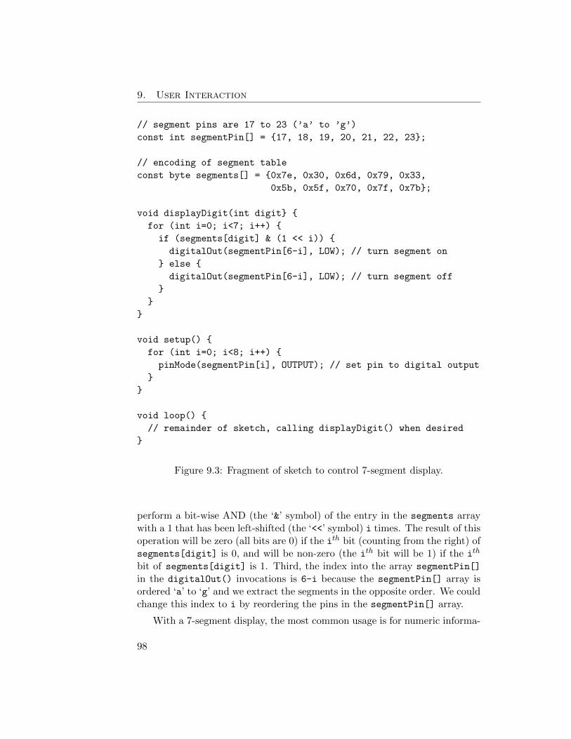
9. User Interaction
// segment pins are 17 to 23 (’a’ to ’g’)
const int segmentPin[] = {17, 18, 19, 20, 21, 22, 23};
// encoding of segment table
const byte segments[] = {0x7e, 0x30, 0x6d, 0x79, 0x33,
0x5b, 0x5f, 0x70, 0x7f, 0x7b};
void displayDigit(int digit} {
for (int i=0; i<7; i++) {
if (segments[digit] & (1 << i)) {
digitalOut(segmentPin[6-i], LOW); // turn segment on
} else {
digitalOut(segmentPin[6-i], LOW); // turn segment off
}
}
}
void setup() {
for (int i=0; i<8; i++) {
pinMode(segmentPin[i], OUTPUT); // set pin to digital output
}
}
void loop() {
// remainder of sketch, calling displayDigit() when desired
}
Figure 9.3: Fragment of sketch to control 7-segment display.
perform a bit-wise AND (the ‘&’ symbol) of the entry in the segments arraywith a 1 that has been left-shifted (the ‘<<’ symbol) i times. The result of thisoperation will be zero (all bits are 0) if the ith bit (counting from the right) ofsegments[digit] is 0, and will be non-zero (the ith bit will be 1) if the ith
bit of segments[digit] is 1. Third, the index into the array segmentPin[]
in the digitalOut() invocations is 6-i because the segmentPin[] array isordered ‘a’ to ‘g’ and we extract the segments in the opposite order. We couldchange this index to i by reordering the pins in the segmentPin[] array.
With a 7-segment display, the most common usage is for numeric informa-
98

9.1. Visual Display
tion; however, if we are displaying hexadecimal numbers, the digits 0 through9 are not sufficient. We can, of course, build any symbol that we wish usingthe individual segments of the display. Table 9.2 extends Table 9.1 (i.e., addsadditional rows), illustrating how one can use a 7-segment display to representhexadecimal output as well.
Table 9.2: Hexadecimal digits in a 7-segment display.
Digit a b c d e f g Display
A on on on off on on on
B off off on on on on on
C on off off on on on off
D off on on on on off on
E on off off on on on on
F on off off off on on on
Another thing to notice about a 7-segment display is that the number ofsegments is less than the number of bits in a byte. When we encoded whichsegments are to be on or off in the segments[] array of Figure 9.3, the high-order (most significant) bit of every entry was 0, because there was no meaningassociated with that bit.
Designers have taken advantage of that fact and added an additional in-dicator to the traditional 7-segment display to serve as a decimal point. Il-lustrated in Figure 9.4, the eighth segment is denoted by the label h and, likeeach of the other segments, can be turned on and off individually.
Figure 9.4: 7-segment display including decimal point.
The above approach works well for a single-digit display, but frequentlywe are interested in displays with more capability. In the following section,
99

9. User Interaction
we will discuss approaches to arbitrary characters (and images), but first wewill just extend our 7-segment display to more digits.
If we want to implement a 4-digit, 7-segment display, clearly the easiestthing to do is simply position 4 copies of an individual 7-segment display rightnext to one another, as illustrated in Figure 9.5. The difficulty comes in whenwe try to use a sketch like that of Figure 9.3 to control all 4 digits, we don’thave enough output pins to control all 4× 7 = 28 digital outputs required.
Figure 9.5: A 4-digit, 7-segment display.
We can solve this problem by time multiplexing between the 4 digits.Instead of wiring the anode of each segment’s LED through a limiting resistorto +5 V, we wire the anode to a digital output pin (4 pins for 4 digits, assumingthe 7-segment display has a common anode) and the limiting resistor is wiredin series with the cathode. The cathodes of segment ‘a’ for each digit arethen wired together and to a single digital output, with similar wiring for theremaining cathodes of each segment. This is illustrated in Figure 9.6, in whichthe 7-segment displays are shown, the common anode wires to the upper leftare to be connected to digital output pins, and the bused cathode wires to thelower left are to be connected to digital output pins. Note that this requires7 + 4 = 11 pins, instead of the earlier 28 pins.
Figure 9.6: Wiring for 4-digit, 7-segment, common-anode LED display.
In this way, we can send a HIGH to one (and only one) of the digits’ anodeswhile sending a LOW to the segments that we wish to be on for that digit. Ashort time later, we switch the HIGH output to the anode to the next digit,
100

9.1. Visual Display
with the third and fourth digits following on a similar schedule. A sketch thatdoes this is shown in Figures 9.7 and 9.8.
What results is a repeating sequence where one quarter of the time each7-segment display is showing the digit that is desired. If the time associatedwith each digit is approximately 5 ms, the entire 4-digit number is illuminatedevery 20 ms, which is way too fast for our eyes to observe the fact that it isflashing. To us it looks like each ‘on’ segment is on continuously.
9.1.3 Pixel-oriented Displays
The obvious limitation of 7-segment displays is that they are severely limitedin the things that they can effectively portray. While OK for numbers, andusable for hex numbers in a pinch (assuming our users don’t get confused witha b and think it is a 6), there are many other things we would like to be ableto output for users. The first, and most obvious, is arbitrary alphanumericcharacters.
The rest of the display technologies that we will consider are all pixel -based. By this, we mean that individual spots in the display (called pixels)can each be on or off, and the collection of all of the pixels forms an image to beseen by the user. In virtually all pixel-oriented displays, the pixels themselvesare organized in a rectangular grid (e.g., an m by n display has m columnsand n rows of pixels), and hence they are sometimes referred to as a matrixdisplay .
The technology at each pixel can vary quite a bit. The simplest pixel-oriented displays have an LED at each pixel (see Figure 9.9, which shows theinternal schematic of a 5 by 7 display, an appropriate size for one character).However, other technologies include LCDs, plasma displays, vacuum fluores-cent displays (not too common anymore), e-paper, and MEMS micro-mirrors(used in DLP projectors). Some are monochrome (only support a single colorat each pixel), while others support a range of colors at each pixel.
The number of pixels also varies widely, from as small as 5 by 7 pixelsfor displaying an individual character to high-resolution 1080p displays (with1920 by 1080 pixels) for HDTV, and even larger. We will constrain our dis-cussion to the smaller end of the range.
Let’s return to Figure 9.9. The first thing to note is that the display doesnot provide individual connections to each pixel’s LED, but rather ties all theanodes of the LEDs in each column together and ties all the cathodes of theLEDS in each row together. Connections are then made to the columns andto the rows, 5 + 7 = 11 connections, rather than the 5 × 7 = 35 connections
101

9. User Interaction
// digit pins are 24 to 27 (left digit 0 to right digit 3)
const int digitPin[] = {24, 25, 26, 27};
// segment pins are 17 to 23 (’a’ to ’g’)
const int segmentPin[] = {17, 18, 19, 20, 21, 22, 23};
// encoding of segment table
const byte segments[] = {0x7e, 0x30, 0x6d, 0x79, 0x33,
0x5b, 0x5f, 0x70, 0x7f, 0x7b};
int digitCounter = 0;
int digitDivisor = 1000;
int valueToDisplay = 0;
void setDigit(int whichDigit) {
for (int i=0; i<4; i++) {
if (i == whichDigit) {
digitalOut(digitPin[i], HIGH);
}
else {
digitalOut(digitPin[i], LOW);
}
}
}
void displayDigit(int digit} {
for (int i=0; i<7; i++) {
if (segments[digit] & (1 << i)) {
digitalOut(segmentPin[6-i], LOW); // turn segment on
} else {
digitalOut(segmentPin[6-i], LOW); // turn segment off
}
}
}
Figure 9.7: Sketch to control 4-digit, 7-segment display (continued in Fig-ure 9.8).
102

9.1. Visual Display
void setup() {
for (int i=0; i<4; i++) {
pinMode(digitPin[i], OUTPUT); // set pin to digital output
}
for (int i=0; i<8; i++) {
pinMode(segmentPin[i], OUTPUT); // set pin to digital output
}
}
void loop() {
// set valueToDisplay to something interesting
setDigit(digitCounter);
displayDigit(valueToDisplay / digitDivisor);
digitCounter++;
digitDivisor /= 10;
if (digitCounter == 4) {
digitCounter = 0;
digitDivisor = 1000;
}
delay(5);
}
Figure 9.8: Sketch to control 4-digit, 7-segment display (continued from Fig-ure 9.7).
that would be required otherwise. (Some displays swap the anode and cathodeconnections, so pay attention to the schematic for your particular display.)
The second thing to note is that the display only contains the LEDs,yet driving an LED from a microcontroller requires current limiting resistors.Don’t just connect the columns and rows directly to your microcontroller, asthis can damage either the display, the micrcontroller, or both.
We control the display in essentially the same way that we controlled the4-digit, 7-segment display in the previous section, we time multiplex groups ofLEDs and cycle through the groups faster than our eyes can respond. Thereare a number of possible design options for doing this. In what follows below,we will cycle through the columns (with cycling through the rows being analternative design option).
To light an individual LED, the voltage on the column wire must be higher
103

9. User Interaction
Figure 9.9: 5 by 7 matrix display.
than the voltage on the row wire. We therefore cycle through the columns byconnecting each column to a digital output pin and ensuring that one columnoutput is HIGH and the other four column outputs are LOW.
With the columns under appropriate control, we now need to send theappropriate rows LOW to light the LEDs that are to be lit (if the row is HIGH,the LED will not light). We connect a current limiting resistor to each row,and connect the other side of the resistor to a digital output pin. Now, foreach column, we can light the desired LEDs in each row by sending the outputconnected to that row LOW.
9.2 Sound
9.3 Other Senses
9.4 User Input
9.5 User Interface Design
104

10 Computer Architecture
The instruction set architecture (ISA) of a processor is traditionally seen as theboundary between the hardware world and the software world. It is essentiallythe abstraction that allows hardware designers and software designers to co-exist without constantly having to re-engineer everything they do because ofchoices made within the other discipline.
In this chapter, we will consider the underlying computer architecture thatmakes up the AVR microcontroller family. Included in this is the set of ma-chine instructions that are directly executable by the microcontroller. Thesemachine instructions constitute the machine language of the microcontroller.We will also introduce the human-readable and -writable variation of the ma-chine instructions, commonly called assembly language, which is primarily thesubject of the next chapter.
10.1 Basic Computer Architecture
A high-level view of the AVR microcontroller family computer architectureis shown in Figure 10.1. When all of these components are included withina single chip, the chip is referred to as a microcontroller . In a larger, morecomplex processor, the program memory, data memory, and peripherals aretypically off-chip, and the chip is referred to as a microprocessor . Thesedefinitions, however, are far from ubiquitous.
10.1.1 Architecture Components
There are a number of components that make up an AVR microcontroller.Items that are included in a microcontroller that are external to a micropro-cessor are the program memory, the data memory, and the peripherals. Wewill start our discussion with these components.
The AVR has what is called a Harvard architecture, in which the programmemory and the data memory are physically separate memory subsystems,
105

10. Computer Architecture
Figure 10.1: AVR microcontroller architecture. All of these components residewithin an individual integrated circuit chip.
often with distinct properties. In the case of the AVR, the machine instruc-tions are each 16 bits wide, and the program memory is addressable at theinstruction level (i.e., each address in the program memory references a 16-bitstorage location which holds one instruction). The data memory is logically8 bits wide, meaning that each data memory address references an 8-bit stor-age location which holds one byte.
Microcontrollers generally also incorporate some number of peripheralsonto the chip as well, and the AVR is no exception. The AVR microcontrollerincludes digital inputs, digital outputs, analog inputs, and analog outputs inits peripheral set.
The remaining components that make up the microcontroller are some-times referred to as the processor components. The register file is the set ofmemory elements that are internal to the processor yet visible to the program-mer (not necessarily a high-level language programmer, but a programmerwho is writing machine language or assembly language). The arithmetic/logicunit (ALU) is the component that is responsible for most data manipulationoperations (e.g., addition, subtraction, logical and, logical or, etc.).
Two additional memory elements are the program counter (PC) and theinstruction register (IR). The program counter is responsible for keeping trackof the next instruction to be executed, and the instruction register holds thecontents of that instruction inside the processor. The control logic is respon-sible for coordinating all of the operations of the microcontroller. The set of
106

10.2. Instruction Set Architecture (ISA)
operations that result in running code is frequently called the fetch-decode-execute cycle.
10.1.2 Fetch-Decode-Execute Cycle
The fetch-decode-execute cycle proceeds as follows:
Fetch The address that is currently in the program counter is used to accessthe program memory and retrieve (or “fetch”) the instruction to beexecuted. This instruction is placed in the instruction register.
Decode The instruction currently in the instruction register (that has just beenfetched) is provided to the control logic, which interprets (or “decodes”)the instruction to decide three things:
1. What operation is to be performed by the instruction. E.g., is itan addition operation or is it a conditional branch operation? Thisis frequently called the opcode.
2. What operands comprise the data to be operated upon and thelocation to store any results.
3. What is the next instruction to be executed. Unless explicitlychanged, the default next instruction is the one at the next ad-dress following the current instruction. Control flow instructions,however, can alter this default.
Execute The actual actions to be performed by the instruction are carried out(or “executed”). If the instruction is an arithmetic or logical operation,the ALU is involved. If the instruction is a load or store, memory isaccessed. If the instruction is a branch, the program counter is alteredto a new value.
While there are many variations from one processor to another, the abovenotion of a fetch-decode-execute cycle is common to almost all of them.
10.2 Instruction Set Architecture (ISA)
The instruction set architecture (ISA) is an abstraction boundary that essen-tially forms a contract between the hardware world and the software world.It defines what is observable and directly controllable by software, yet doesnot prescribe how the hardware implements the functions.
Traditionally, an ISA comprises the following four components:
107

10. Computer Architecture
• register file – the programmer-visible storage within the processor (vis-ible to the machine language programmer, not a high-level languageprogrammer).
• memory model - the logical organization of the memory (as viewed bythe machine language program).
• instruction set – the collection of machine language instructions thatare directly executable by the processor.
• operating modes – some processors have subsets of the instructionsthat are privileged based on being in a given “mode”.
We will consider each of the above ISA elements in turn. By necessity, wewill not cover the complete ISA of the AVR microcontroller, but will insteadprovide a representative subset. Full details of the AVR can be found in theinstruction set manual from Atmel [1].
10.2.1 Register File
The register file is the machine language program’s view of storage that isinternal to the processor. In the AVR microcontrollers, this is comprised of32 general purpose registers (named r0 to r31) and a status register (namedSREG).
The general purpose registers are each 8 bits wide. To store 16-bit values,they are normally paired (e.g., r31:r30) with the high-order bits of the 16-bitvalue going in the odd-numbered (larger label) register and the low-order bitsgoing in the even-numbered (smaller label) register.
The general purpose registers can hold data or addresses; however, regis-ters r26 through r31 are commonly used for addresses, and as such have syn-onyms associated with each of three register pairs. The register pair r27:r26is also known as X, r29:r28 is also known as Y, and r31:r30 is also known asZ. We will see examples of the use of these register pairs for addressing later,for now it is sufficient to know that they have more than one name.
The status register, SREG, is an 8-bit register that gives information aboutwhat has happened previously on the processor. Informally, what is the pro-cessor’s “status”?
More precisely, it comprises 8 individual status bits, each of which has itsown dedicated function. Tabletbl:sreg gives the meaning and shorthand labelfor each bit of the status register.
108

10.2. Instruction Set Architecture (ISA)
Table 10.1: Bits of status register SREG.
Bit 7 6 5 4 3 2 1 0
Label I T H S V N Z C
Meaning interrupt transfer half sign signed negative zero carryenable bit carry bit overflow flag flag flag
As an example of how the status register operates, when the processorexecutes an add instruction, if the result of the addition is negative (i.e., if themost significant bit of the result is 1), the N bit in the SREG will be set to 1,otherwise it will be set to 0. Likewise, if the result of the addition is zero, theZ bit will be set to 1, otherwise it will be set to 0. Subsequent instructions(e.g., conditional branches) can then test the value of individual bits in SREG
and act accordingly.
10.2.2 Memory Model
The memory model is essentially the machine language programmer’s view ofsystem memory. In the AVR microcontroller family, there are several itemsthat can be accessed through the memory interface.
Program Memory
The AVR’s Harvard architecture means that the program memory is separatefrom the data memory. The program memory is constructed using flash mem-ory technology, which has the advantage that it is non-volatile. It retains itscontents even when the power is removed.
As a result, if you provide power to an Arduino board and don’t downloada new program, it will run the last program that was downloaded, since thatis what the processor finds when it fetches instructions from the programmemory.
Because most instructions in the AVR family are 16 bits in length, thedesigners chose to have the program memory organized around 16-bit words.This means that an individual address that points to a single location in theprogram memory is referring to a 16-bit value.
The program memory is further divided into application program memoryand a boot loader. The boot loader is responsible for receiving new programsfrom the USB link, loading them into application program memory, and start-ing them up. If no new program comes from the USB, then the boot loaderstarts up the program that is currently resident in the application programmemory.
109

10. Computer Architecture
Data Memory
The primary memory used by programs is the data memory. It is the mem-ory that is accessed on load and store instructions. Data memory is byteaddressable, meaning that each address refers to an individual byte, or 8 bits.
The largest region of data memory is SRAM that is internal to the chip andavailable to store variables or anything else desired by the program. SRAM, orStatic Random Access Memory, is a memory technology that supports single-cycle read and write operations to any location (address) in the memory.SRAM is volatile, so when power is lost, the contents stored in memory arenot retained.
In addition to the internal SRAM, addresses in data memory are used toaccess other structures, described below.
Non-volatile Memory
The third memory type is program-accessible non-volatile memory, which isconstructed using EEPROM technology. EEPROM, or Electrically ErasableProgrammable Read Only Memory, is a memory technology that, like flash,does not lose its contents when power is removed. Like the data memory, itis 8 bits wide and byte addressable. The major difference between EEPROMand flash is that EEPROM can be altered (erased and rewritten) one byte ata time, where flash is typically bulk erased and then rewritten.
Peripherals
Chapters 2 through 5 discussed approaches to send signals in and out of themicrocontroller. Devices that are attached in this way are called peripherals.In the AVR instruction set architecture, there are two mechanisms for access-ing peripherals: (1) in and out instructions, and (2) through the memoryinterface.
The in and out instructions allow for quick (single execution cycle) accessto 64 addresses on what is called an I/O bus. Individual peripherals areassigned to unique addresses on this bus, and it is common to call individuallocations on the bus I/O registers. With 64 addresses on the I/O bus, therange of I/O addresses is from 0x00 to 0x3F.
In addition to being available on the I/O bus, the I/O registers can also beaccessed via the memory interface (i.e., they also have addresses in the datamemory). The I/O registers start at memory location 0x0020, so that I/Oaddress 0x00 accesses the same I/O register as memory location 0x0020, I/O
110

10.2. Instruction Set Architecture (ISA)
address 0x01 is the same I/O register as memory location 0x0021, and I/Oaddress 0x3F is the same as memory location 0x005F.
Because the number of needed addresses has grown over time, the AVRfamily supports an extended set of I/O registers, beyond the original 64. Theseextended I/O registers are are not available via the in and out instructions,but are only available via the data memory, starting at data memory loca-tion 0x0060 and running through 0x00FF. The internal SRAM then starts atmemory location 0x0100.
In addition to the above items, the memory interface can also be used asan alternative path to access the processor’s state. This includes not onlythe register file described in Section 10.2.1, but also additional registers thatcomprise part of the processor’s workings. The register file is accessible asdata memory addresses 0x0000 through 0x001F, and the remaining registersare included in either the I/O registers or the extended I/O registers.
Table 10.2 shows some of the peripherals that can be accessed by the pro-gram through the memory interface. Both the data memory address and theI/O address are shown along with the label and description of the peripheral.
Several of the table entries are worth specific mention. Memory addresses0x0023 through 0x002B (I/O addresses 0x03 through 0x0B) comprise threegroups of addresses, and within each group there are three addresses associatedwith an I/O port . These 8-bit registers are the interface to the digital outputand input pins described in Chapters 2 and 3. Each port is associated withup to 8 physical pins on the chip.
Within each group, DDRx is the data direction register, which is used to setwhether each pin is an INPUT or an OUTPUT in response to a call to pinMode().The PINx addresses are used to read the input values for digitalRead(), andthe PORTx addresses are used to write output values using digitalWrite().
Memory address 0x005F (I/O address 0x3F) is the status register, SREG,described in Section 10.2.1. Memory address 0x0060 is a watchdog timercontrol register. A watchdog timer is a circuit that independently keeps trackof time and is used to ensure that the software on the processor continues tooperate. Based on a settable timeout value, the software is required to “reset”the watchdog time prior to the timeout. If this watchdog timer reset does nothappen, the watchdog timer circuitry will reset the processor, in an attemptto correct whatever problem caused the software to miss its deadline.
Other entries in the I/O address space (not shown in the table) provideaccess to the free-running counter used for timing that was described in Chap-ter 6 and control other aspects of the processor’s operation.
111

10. Computer Architecture
Table 10.2: Peripherals accessible through the memory interface.
Memory I/O Label MeaningAddress Address
0x0000 – r0 general purpose register r00x0001 – r1 general purpose register r1
. . . .
. . . .
. . . .0x001E – r30 general purpose register r300x001F – r31 general purpose register r31
0x0020 0x00 – reserved0x0021 0x01 – reserved0x0022 0x02 – reserved0x0023 0x03 PINB input pins port B0x0024 0x04 DDRB data direction register port B0x0025 0x05 PORTB data register port B0x0026 0x06 PINC input pins port C0x0027 0x07 DDRC data direction register port C0x0028 0x08 PORTC data register port C0x0029 0x09 PIND input pins port D0x002A 0x0A DDRD data direction register port D0x002B 0x0B PORTD data register port D
. . . .
. . . .
. . . .0x005D 0x3D SPL stack pointer (low byte)0x005E 0x3E SPH stack pointer (high byte)0x005F 0x3F SREG status register (see Table 10.1)
0x0060 – WDTCSR watchdog timer control register. . . .. . . .. . . .
0x0078 – ADCL analog-to-digital conv. register (low byte)0x0079 – ADCH analog-to-digital conv. register (high byte)
. . . .
. . . .
. . . .0x00FF – – reserved
112

10.2. Instruction Set Architecture (ISA)
Memory Map
The memory model can be shown visually in a diagram known as a memorymap. Figure 10.2 shows the memory map for the AVR microcontroller usedin the Arduino Uno.
Figure 10.2: AVR microcontroller memory map.
There is a separate rectangle for each memory subsystem, the programmemory, data memory, and non-volatile memory. The width (in bits) of eachmemory subsystem is shown across the top of the rectangle that representsthat memory. Addresses (starting at the top and increasing as you look down)are indicated immediately to the left of the rectangle, and different regionswithin the memory are indicated within the rectangle.
10.2.3 Instruction Set
The third component of the instruction set architecture, after the registerfile and the memory model, is the actual instructions themselves. These arethe specific instructions that can be directly executed by the processor, themachine language of the AVR family of microcontrollers.
113

10. Computer Architecture
The AVR family is what is known as a 2-address, load/store machine.As such, most instructions operate to and from the register file, rather thaninteract with memory. The “2-address” label means that instructions reference2 registers, and one of the registers acts both as a source of data and thedestination for the result. The “load/store” label means that explicit loadand store instructions move data back and forth between memory and theregister file and the operations happen on data in the register file.
Classes of Instructions
We will separately consider instructions as members of several classes, orgroups: arithmetic operations, logical operations, control flow, data move-ment, and system operations.
The following syntactic conventions will be used as part of the descriptionsof individual instructions and the addressing modes that follow:
• Rd – destination register (one of r0 to r31)
• Rs – source register (one of r0 to r31)
• k – constant
• X, Y, Z – index register (X is r27:r26, Y is r29:r28, Z is r31:r30)
The arithmetic operations include addition, subtraction, increment, decre-ment, complement, and multiplication (but not division). Let us examine theadd instruction in some detail. The syntax for a register to register additionis as follows:
add Rd,Rs
The operation that gets performed is
Rd← Rd + Rs
in which the initial value in Rd is added to the value in Rs and the result isstored as the new value of Rd.
Also, the individual bits of the status register, SREG, are set or clearedbased upon the value of the result. In particular, six of the eight bits of SREGwill be altered based on the results of the add instruction. Table 10.3 showshow they are effected. The remaining two bits in SREG are not changed by theinstruction.
114

10.2. Instruction Set Architecture (ISA)
Table 10.3: SREG bits effected by add instruction.
Label Name Definition
H half carry set if carry from bit 3S sign bit N ⊕ V, for signed testsV signed overflow set if two’s complement overflowN negative flag equal to most significant bit of the resultZ zero flag set if result is 0x00C carry flag set if carry from bit 7 (msb)
Similar to the add instruction, the adc (add with carry) instruction is usedto perform additions on data elements that are larger than 8 bits. The syntaxis
adc Rd,Rs
and the operation that gets performed is
Rd← Rd + Rs + C.
The value in Rd is added to the value in Rs, plus the carry bit, C, of the statusregister, SREG. The result is stored in Rd. If we wanted to add the 16-bit valuein the register pair r7:r6 to the 16-bit value in the register pair r9:r8, thecode would be as follows:
add r6,r8
adc r7,r9
in which the add instruction sums the lower order bits in r6 and r8, with anycarry out being placed in the C bit of SREG. The subsequent adc instructionsums the higher order bits in r7 and r9, including any carry from the lowerorder bits’ sum.
Some instructions require only one operand. For example,
inc r17
increments (adds one to) register r17.
The logical operations include AND, OR, NOT, exclusive-OR, shift, andset/clear bits. Expressing logical operation instructions is very similar toarithmetic operations. Consider the logical AND operation. The syntax is
and Rd,Rs
115

10. Computer Architecture
while the operation that gets performed is
Rd← Rd ∧ Rs
where each bit of Rd is combined with each bit of Rs using the logical ANDoperation with the result stored in Rd.
The normal instruction flow is once an instruction has completed its exe-cution, the next instruction in program memory is fetched. Control flow in-structions are those that have the potential to change this normal flow. Theseinclude unconditional control flow operations, such as jumps, subroutine call,and return, as well as conditional control flow operations, often called branchinstructions.
Branch instructions will either branch or not branch, based on a Booleancondition that is tested as part of the instruction. Most branch instructionsare conditional on one or more bits in the status register, SREG. For example,the brne instruction (branch if not equal) will branch if the Z bit of SREG isclear. This instruction might come immediately after a compare instruction,e.g., the instruction sequence
cp r3,r22
brne loop
first compares register r3 with r22, which will set the Z bit of SREG if r3 − r22
is equal to zero (i.e., if r3 and r22 are equal). The conditional branch instruc-tion then branches to the program location labeled loop if the two registersare not equal to one another (i.e., the Z bit is not set).
Data movement instructions includes register to register transfers, loadand store instructions that move data back and forth between registers andmemory, and I/O instructions that move data to/from peripheral devices..The simplest data movement instruction copies data from one register to an-other (leaving the source register unaltered). E.g.,
mov r23,r22
copies the contents of r22 into r23. Note, mov might make you think of theword “move”; however, it leaves the source register unchanged, so “copy” is abetter way to think about what the instruction actually does. We can load aconstant value into a register using the load immediate instruction:
ldi Rd,k
116

10.2. Instruction Set Architecture (ISA)
which loads the constant value k into register Rd.
When a load instruction is reading a value from memory, there are anumber of methods that can be used to specify the address in memory to beread. The simplest of these is to directly specify the address as part of theinstruction, with the load direct from data space instruction:
lds Rd,k
which accesses the memory at address k and copies the contents of memoryat address k into register Rd. Other methods for specifying the address to beaccessed are called addressing modes and are described below.
Similar to the load direct from data space instruction is the store directto data space instruction:
sts k,Rs
which copies the data in register Rs and stores it in the memory location ataddress k.
While it is possible to access all the peripheral devices via the memorysystem (see memory map in Figure 10.2), there are also dedicated instructionsfor accessing the I/O registers in less time (and smaller instruction size) thanload and store instructions. The in instruction supports reading from an I/Operipheral:
in Rd,k
reads data from I/O register k (0 ≤ k ≤ 63) into general purpose register Rd,and the out instruction writes to an I/O peripheral:
out k,Rs
sends the contents of general purpose register Rs to I/O port k.
Finally, there are a number of system operations that don’t convenientlyfit into any of the categories above. For example, the nop is “no operation”(it is an instruction that has no effect other than to take time to execute) andthe wdr instruction is the watchdog timer reset instruction.
Addressing Modes
Instructions that operate on data must first identify the input data to theoperation and identify the location in which to store the result. Generally,
117

10. Computer Architecture
techniques used to specify either data source or destination are called ad-dressing modes, and the AVR has a number of addressing modes which wewill describe below.
Unfortunately, there is great disparity in the naming of addressing modes,so we will use the commonly used name in the description, but will also in-clude the specific name that Atmel uses in its documentation for the AVRmicrocontroller family.
The simplest addressing mode is immediate. Here, the value to be operatedon is included as part of the instruction itself. As an example, if we have avalue in register r9 and we wish to subtract 7 from that value, the 7 is partof the instruction, e.g.,
subi r9,7
in which the operation to be performed is as follows:
r9← r9− 7
and the fact that the addressing mode is immediate is conveyed as part of theinstruction, subtract immediate, subi.
The most commonly used addressing mode is register addressing . (Atmelcalls this “register direct.”) In this case, the source (or destination) of datais one of the 32 general purpose registers. In the example above, the 7 isimmediate addressing and the register r9 is register addressing. In this case, r9is both a source and destination. The majority of operations to be performedon data use the register addressing mode, enabling efficient data movementfrom the register file to the ALU and back to a register.
The first addressing mode we will cover that accesses memory is directaddressing. (Atmel calls this “data direct” or “I/O direct.”) In direct ad-dressing, the address in memory is directly specified in the instruction. In thecase of a load instruction, the source is a memory address, e.g.,
lds r12,0x0500
loads the value in memory location 0x0500 into register r12. In the case of astore instruction, the destination is a memory address, e.g.,
sts 0x1000,r12
stores the value currently in r12 into memory location 0x1000. Direct ad-dressing is also appropriate for accessing the I/O registers using the in andout instructions as well. In this case, the address specified is not a memoryaddress, but rather an I/O address (in the range 0 to 63).
118

10.2. Instruction Set Architecture (ISA)
While direct addressing works well when the address to be accessed isknown when the program is written, it isn’t as useful if the address dependson the program input. Consider the case of an array reference. Which specificaddress we wish to access depends upon the value of the array index.
To enable the address to be computed at run time, we use the indirectaddressing mode. (Atmel calls this “data indirect.”) Recall that 3 registerspairs (r27:r26, r29:r28, and r31:r30) have alternate names (X, Y, and Z,respectively). The register pairs are sometimes called index registers. Theindirect addressing mode uses the contents of one of these register pairs as theaddress of the data to be loaded (read) or stored (written).
For example, the instruction sequence below:
ldi r26,0x00
ldi r27,0x05
ld r12,X
first puts 0x0500 into the index register X (the least significant byte into r26
and the most significant byte into r27) and then loads the value at memorylocation 0x0500 into register r12 (using the ld instruction). Similarly, theinstruction sequence
ldi r28,0x00
ldi r29,0x10
st Y,r12
puts 0x1000 into the index register Y and then stores the value initially inregister r12 into memory location 0x1000.
The indirect addressing mode can be extended to also alter the indexregister used to access memory. In the post-increment mode, the index registeris incremented after being used to access memory. In the pre-decrement mode,the index register is decremented prior to being used to access memory. Thesyntax for a post-increment indirect access is
ld Rd,Y+
for a load, and the syntax for a pre-decrement indirect access is
st -Z,Rs
for a store.
There are a few specialized addressing modes for program memory access;however, we will not discuss them here.
119

10. Computer Architecture
10.2.4 Operating Modes
Complex processors often have different operating modes, in which differentsubsets of the instruction set are enabled or not enabled. For example, thecontrol mechanisms for the virtual memory subsystem on an Intel processorin a PC cannot be accessed by a regular user’s program.
The Atmel AVR family does not effectively have operating modes, so wecan avoid the subject, other than to include it in the list of what constitutesa processor’s ISA.
120

11 Assembly Language
In the examples of instructions provided in Chapter 10, we actually cheateda bit. In the real machine, instructions are binary values (typically 16 bits inlength) that are stored in the program memory. The examples we providedare actually written in a more human-readable form called assembly language.
In this chapter, we will clarify the distinction between assembly languageand machine language, as well as discuss the options available to the assem-bly language programmer that do not get translated (directly) into machinelanguage. Once a program has been expressed in assembly language, a tool(called the assembler) translates the assembly language source code into ma-chine language (often called object code). We will also spend some time dis-cussing how to author good assembly language code, including how to mixassembly language and high-level language code in one sketch.
11.1 Machine Instructions
The individual instructions that are stored in the program memory and aredirectly executed by the processor constitute the machine language of theprocessor. Machine language instructions are encoded in binary, with the bitpattern both specifying the operation itself (i.e., the opcode) and the operands(i.e., source and destination of the data).
For example, the encoding for several representative instructions is givenin Table 11.1. Some of the table entries are for specific operands, and othersshow how to encode the operands in the instruction word. When encodingoperands, the general purpose registers are numbered 0 to 31, requiring 5bits to specify. Register Rd is specified using the 5-bit value d4d3d2d1d0 andregister Rs is specified using the 5-bit value s4s3s2s1s0. Constants are specifiedin a similar way, with the distinction that different constants have differentnumbers of bits allocated in the instruction format. Almost all instructionsare 16 bits, with a few having an additional 16-bit word (that immediately
121

11. Assembly Language
Table 11.1: Machine language encoding of several instructions. In the table,di is bit i of Rd, si is bit i of Rs, and ki is bit i of k.
Instruction 15 14 13 12 11 10 9 8 7 6 5 4 3 2 1 0
nop 0 0 0 0 0 0 0 0 0 0 0 0 0 0 0 0
wdr 1 0 0 1 0 1 0 1 1 0 1 0 1 0 0 0
inc Rd 1 0 0 1 0 1 0 d4 d3 d2 d1 d0 0 0 1 1
inc r12 1 0 0 1 0 1 0 0 1 1 0 0 0 0 1 1
ld Rd,X 1 0 0 1 0 0 0 d4 d3 d2 d1 d0 1 1 0 0
ld r6,X 1 0 0 1 0 0 0 0 0 1 1 0 1 1 0 0
mov Rd,Rs 0 0 1 0 1 1 s4 d4 d3 d2 d1 d0 s3 s2 s1 s0mov r3,r1 0 0 1 0 1 1 0 0 0 0 1 1 0 0 0 1
add Rd,Rs 0 0 0 0 1 1 s4 d4 d3 d2 d1 d0 s3 s2 s1 s0add r7,r4 0 0 0 0 1 1 0 0 0 1 1 1 0 1 0 0
subi Rd,k 0 1 0 1 k7 k6 k5 k4 d3 d2 d1 d0 k3 k2 k1 k0subi r21,2 0 1 0 1 0 0 0 0 0 1 0 1 0 0 1 0
lds Rd,k 1 0 0 1 0 0 0 d4 d3 d2 d1 d0 0 0 0 0
k15 k14 k13 k12 k11 k10 k9 k8 k7 k6 k5 k4 k3 k2 k1 k0lds r8,0x100 1 0 0 1 0 0 0 0 1 0 0 0 0 0 0 0
0 0 0 0 0 0 0 1 0 0 0 0 0 0 0 0
follows in program memory).
Note an interesting feature of the subi instruction, subtract immediate.It only has 4 bits to specify Rd, the destination register. Instead of beingavailable to use on all 32 general purpose registers, the subi instruction canonly operate on registers r16 to r31, and the register Rd is specified by thebits 1d3d2d1d0.
Restrictions like the one above are fairly common in the machine languageof many processors. With only 16 bits to specify the full instruction, the de-signer of the instruction set often must choose whether to give access to thefull range of registers (requiring 5 bits of the 16 available in the instructionword) or limit the range of registers accessible and increase the range of con-stants that can be specified (in this case, enabling constants of length 8 bits,which can range in value between −128 and +127).
11.2 Assembly Language Instructions
In the code examples of Section 10.2.3 and in the left-most column of Ta-ble 11.1, we have been using the assembly language expressions for the in-structions of interest. The general form for assembly language instructions
122

11.3. Labels and Symbols, Constants and Numbers
is:
label: opcode operands ;comments
where the label in an optional identifier (specifically, an identifier of theaddress in program memory where the instruction is stored), the opcode isthe name of the instruction itself, sometimes called an operation code, theoperands specify the source and/or destination of the data needed to exe-cute the operation, and the comments are ignored by the program (they areintended for the human reader).
It is conventional for the semi-colon (;) to delimit comments in assemblylanguage. However, in modern assemblers C/C++ style comments (either //or /* */) are also commonly recognized.
11.3 Labels and Symbols, Constants and Numbers
Whenever the programmer inserts a label into the assembly language source,that declares a symbol (within the assembly process) that can then be usedelsewhere in the program. An immediately obvious use of this capability is toprovide labels whenever a program might wish to do conditional branching.
Consider the following code snippet:
ldi r3,2 ; r3 <- 2
loop: add r7,r8 ; r7 <- r7 + r8
dec r3 ; r3--
brne loop ; branch if r3 <> 0
in which r3 is initialized to 2, and after r8 has been added to r7, r3 isdecremented by one. The decrement instruction, dec, sets the Z bit in SREG
to 1 if the result of the decrement is zero. The first time that dec is executed,the result is not zero, so the brne instruction (BRanch if Not Equal to zero)will take the branch to loop, which has been declared to be the address ofthe add instruction. Once r3 does equal zero, the brne instruction no longerbranches, and the code executes the instruction that immediately follows brne.
Another observation to make is that when initializing r3 to the value 2, wedid not specify the base. By default, when constants are specified in assemblylanguage, they are in base 10 (as is the case in higher-level languages likeC/C++ and Java). There are a variety of ways that alternative bases canbe expressed, and the assembly language programmer must check the manualof the specific assembler being used to know which is correct. We will stick
123

11. Assembly Language
with the same convention used in C/C++ and Java, that a 0x preceding thenumeric constant means that the constant is being expressed in hexadecimal.
11.4 Assembly Language Pseudo-operations
In addition to assembly instructions that translate directly in machine instruc-tions, the assembler also recognizes instructions that in reality are aimed at theassembler itself. These pseudo-operations (or pseudo-ops) are also sometimescalled assembler directives.
To distinguish pseudo-ops from regular instructions, it is conventional forthem to begin with a period (.) as the first character of the operation. Forexample,
.equ portd,0x0b
uses the .equ pseudo-operation to define the symbol portd as equivalent tothe expression 0x0b. That symbol can then be used in place of a numericalconstant in a subsequent in or out instruction, such as
in r7,portd ;read from I/O port 0x0b
which reads from the I/O port 0x0b but references the port using the symbolicname portd.
11.4.1 Sections
One of the tasks required of the assembly language programmer is to specifywhat items are to be assigned to the various memories. On the AVR family,the code goes into the program memory (often called the text section or textsegment), and the data is either in the non-volatile memory (EEPROM) ordata memory (SRAM). The SRAM is, in assembly language terms, called thedata section or data segment.
11.4.2 Data Section Pseudo-ops
The data section starts with the following pseudo-op:
.data
which declares that the assembly language statements to follow are associatedwith the data memory (SRAM).
124

11.4. Assembly Language Pseudo-operations
There are a collection of pseudo-ops that are supported in the data sectionfor reserving space in the data memory. The simplest is .byte, which reservesspace and gives it an initial value, i.e.,
label: .byte expression[,expression]
which reserves one byte for each expression (the second and subsequent onesare optional) and initializes it with the value of expression. The inclusionof the label associates the symbol label with the address of the first byteallocated.
We can make label into a global symbol (visible to the linker) throughthe use of the .global pseudo-op:
.global label
however, be careful to remember that the linker does not have any notion oftype, so it is only the address of label that is available to other files.
We can allocate a C-style string (null-terminated) via the .asciz pseudo-operation, e.g.,
errstr: .asciz "Error"
reserves 6 bytes of data memory and initializes it to the ASCII characters ’E’,’r’, ’r’, ’o’, ’r’, and ’\0’. The label errstr is associated with the firstaddress in the string.
Arbitrary sized chunks of data memory can be allocated with the .space
pseudo-op, which takes two arguments, the size of the chunk of memory toreserve (in bytes) and the value to store in each byte. For example,
array1: .space 10,0
will reserve 10 bytes of memory (initialized to 0) and associate the label array1with the first allocated byte.
11.4.3 Text Section Pseudo-ops
The text section starts with the following pseudo-op:
.text
which declares that the assembly language statements to follow are code (pro-gram instructions).
125

11. Assembly Language
If we wish a label declared in the .text section to be available to the linker(i.e., enabling it to be called from another file), we again use the .global
pseudo-op. The .equ directive is also available to use in the .text section.
Another commonly used directive is .include, which enables another fileto be directly inserted at the point of the directive, e.g.,
.include "header.h"
will insert the contents of the file header.h at the current point in the assemblylanguage source.
11.4.4 Macros
With the .macro directive, it is possible to declare macros that can do fairlysophisticated symbolic processing at assembly time. We will not describe thegeneral technique for declaring macros; however, we will illustrate the use oftwo very useful macros that are built-in to the assembler.
When using an 8-bit processor, it is common to manipulate 16-bit values(e.g., addresses) one byte at a time. The assembler provides two macros thatare useful in this process, i.e,
lo8(value)
takes a 16-bit value and returns the least significant 8 bits, while
hi8(value)
takes a 16-bit value and returns the most significant 8 bits. These macroscan be very useful in address manipulation, especially for array indexing.
For example, if we wish to load the address of array1 into the X indexregister (recall X is a name for the register pair r27:r26), we can use thefollowing instruction sequence:
ldi r26,lo8(array1)
ldi r27,hi8(array1)
ld r2,X
which loads the value stored at address array1 into register r2.
126

11.5. Authoring in Assembly Language
11.5 Authoring in Assembly Language
It is true that when authoring applications in assembly language, the program-mer can do pretty much whatever he or she wants to do, given the only theconstraints of the instruction set. That approach, however, is rarely a goodidea. The conventions that have come in to common practice using high-levellanguages (even simple things like if-then-else statements and while loops)came into being for good reasons. Next, we will examine a number of thoseconventions, and explore how to author assembly language application codein such a way as to reap the benefits of those conventions.
11.5.1 Accessing Data
When accessing data in a high-level language like C or Java, the programmerdeclares variables of a given type, and the compiler is responsible for assigningstorage locations for those variables. The programmer can then read the databy simply referencing the appropriate variables in expressions.
In assembly language, things happen at a lower level of abstraction. Whatis directly accessible to the assembly language programmer is the register setand memory model of the AVR microcontroller. What data are to be storedin registers vs. what data are to be stored in memory is the responsibility ofthe programmer. In addition, each register is only 1 byte (8 bits) in size, andeach individual memory location is also only 1 byte wide. A C int is 2 bytes(16 bits) in size, so it requires two registers or two memory locations.
Since the AVR is a load/store architecture, accesses to memory are all viaload or store instructions. Data manipulations, such as add, subtract, etc.,read from registers and write their results to registers. As such, if we want toadd the contents of two memory locations, we must first load the data intoregisters, perform the add operation, and then store the result to memory.
Consider the following code snippet:
lds r18,0x0200 ;M[0x0250] <- M[0x0200] + M[0x0210]
lds r19,0x0210
add r18,r19
sts 0x0250,r18
its purpose is indicated in the comment on the first line, add the contents ofmemory location 0x0200 to the contents of memory location 0x0210 and storethe result in memory location 0x0250. It accomplishes this by loading the twovalues into registers r18 and r19, adding r19 to r18 (leaving the result in r18)and storing the result in memory location 0x0250.
127

11. Assembly Language
The above is an example of how an operation that only takes one lineof source code in a high-level language actually takes 4 assembly languageinstructions to accomplish the same thing. And the above example only worksfor single-byte data (e.g., a char in C). What about an int, or a long int?
Multi-byte Primitive Data Elements
There are two approaches commonly used to store multi-byte primitive dataelements in byte-sized locations. Either approach uses adjacent locations forstorage (e.g., if in the register set, use a pair of registers such as r16 andr17 to store a two-byte value), they differ in which byte gets stored in whichlocation. The AVR microcontroller is what is called a little-endian machine.What this means is that the low-order bits of the multi-byte value get storedin the location with the smaller address or label. In our earlier example, if thetwo-byte value 0x1f32 were being stored in the registers r16 and r17 (denotedas register pair r17:r16), the low-order byte, 0x32, gets stored in r16 and thehigh-order byte, 0x1f, gets stored in r17.
In the register set, we reference pairs of registers by listing them both (e.g.,the r17:r16 example above). When talking about multi-byte values stored inmemory, the convention is to discuss the data value as if it were stored in oneaddress, even though it actually consumes more than one memory location.So, a two-byte value that is referred to as being stored at location 0x02f4
actually consumes memory location 0x02f4 and location 0x02f5 (recall thatmemory addresses are 16 bits long on the AVR microcontroller, it is the mem-ory cells themselves that are 8 bits wide). Since it is a little-endian machine,the low-order byte gets stored in location 0x02f4 and the high-order byte getsstored in location 0x02f5.
The second approach (which is the opposite of a little-endian machine)is a big-endian machine. In a big-endian machine, the high-order byte ofa multi-byte value is stored in the location with the smaller address. TheNXP ColdFire processors (originally developed by Motorola) are an exampleof big-endian machines. The big-endian convention is also known as networkorder, as the high-order byte of multi-byte values are typically sent first indata communications (we will return to this issue in Chapter 12).
On our little-endian AVR microcontroller, if we wish to load a 16-bit valuefrom memory address 0x2f4 into the register pair r17:r16, the code wouldbe as follows:
lds r16,0x02f4
lds r17,0x02f5
128

11.5. Authoring in Assembly Language
and it takes two load instructions, one per byte. We can accomplish the samegoal in a slightly more general way by using one of the address registers:
ldi r26,0xf4 ;X <- 0x02f4
ldi r27,0x02
ld r16,X+ ;r17:r16 <- M[02f4]
ld r17,X
which has a number of things going on. First, we are using address registerX, which is actually the pair of registers r27:r26, so it must be initializedto 0x02f4, which happens in the first two instructions. Second, take a lookat the comment associated with the first two instructions. See what it isdoing? It is telling us higher-level information than the literal statements inassembly language. The instruction with the comment, and the instructionimmediately below it, serve the high-level purpose of storing the value 0x02f4
in the X address register. Third, the next instruction (after initializing theaddress register) loads the low-order byte into r16. It uses the post-incrementaddressing mode, so that after address register X has been used to accessmemory, it is incremented by 1 (so it now has the correct value to accessthe high-order byte of our two-byte data). Fourth, we finish by loading thehigh-order byte from location 0x02f5 into register r17. Again, the commentassociated with the last two instructions describes the high-level intentionsof the programmer, specifically, to load the contents of memory at address0x02f4 into the register pair r17:r16.
In addition to two-byte elements (such as int), we also want to occasionallydeal with four-byte elements (such as long int or float). The general rulethat applies to two-byte values extends just as one would expect for largervalues. The least significant byte is stored in the lowest memory addressand the most significant byte is stored in the highest address. Figure 11.1illustrates the memory layout for both little-endian and big-endian machines.
Arrays
While the order in which the individual bytes of a primitive data type arestored in memory depends upon whether a machine is little-endian or big-endian, the order in which array elements are stored has no such dependency.In C, array indices start at 0, and increment up. The memory locations usedto store array elements do exactly the same.
Consider the C string declared as follows:
char str[5] = "read";
129

11. Assembly Language
little-endian
8 bits
0x050E0x050F
0x0600
0x0603
least sig.most sig.
least sig.
big-endian
8 bits
2-bytevalue
4-bytevalue
most sig.
most sig.least sig.
most sig.
least sig.
0x06010x0602
increasingaddress
Figure 11.1: Two-byte and four-byte memory layout for little-endian and big-endian machines. The 2-byte value is located at address 050e and the 4-bytevalue is at address 0x0600.
Table 11.2: Memory layout of array str.
C reference Address Value
str[0] str + 0 ’r’
str[1] str + 1 ’e’
str[2] str + 2 ’a’
str[3] str + 3 ’d’
str[4] str + 4 ’\0’
it will have 5 array elements, and the memory layout will be as shown inTable 11.2.
In assembly language, this array would be declared (in the data segment)and initialized as follows:
.data
str: .asciz "read"
which essentially does close to the same thing as the C declaration above.It allocates 5 bytes in memory, initializes those bytes to the characters inthe string "read" (including the terminating NULL character), and declaresthe symbol str to refer to the address of the first element. The primary
130

11.5. Authoring in Assembly Language
difference is that C understands the type of str to be an array of chars,while in assembly language, the symbol str merely represents the address ofthe memory location, it has no type information.
If we want to write assembly language code to implement the following Cstatement,
str[3] = ’l’;
which will edit the string from "read" to "real", we again use an addressregister. This time we’ll use address register Z, just to be different.
The assembly language code is shown in Figure 11.2, in which the firsttwo instructions put the address of the array str into the address registerZ (taking advantage of the macros hi8() and lo8() described earlier in thechapter), the third instruction changes Z to be the address of the 4th elementof str (by adding 3, remember that the first element is designated by index0), the next to last instruction puts the ASCII code for the letter l into r16,and the last instruction stores the letter into str[3].
ldi r30,lo8(str) ;Z <- &str[3]
ldi r31,hi8(str)
adiw r31:r30,3
ldi r16,’l’ ;r16 <- ’l’
st Z,r16 ;str[3] <- r16
Figure 11.2: Assembly language array access.
If the array is an array of multi-byte values (e.g., an array of ints), thenthe order of elements in memory is the same (start at index 0 and increase);however, each element now consumes more than one byte of storage. If, forexample, the elements are each two bytes, then the address increase for eachelement must be two. The element itself is stored with its normal byte ordering(least significant byte first for the AVR microcontroller).
Consider the 5-element integer array item, which would be declared in Cas follows:
int item[5];
and declared in assembly language as:
item: .space 10,0
131

11. Assembly Language
Table 11.3: Memory layout of item array.
C reference Address Contents
item[0]item + 0 least significant byte of item[0]item + 1 most significant byte of item[0]
item[1]item + 2 least significant byte of item[1]item + 3 most significant byte of item[1]
item[2]item + 4 least significant byte of item[2]item + 5 most significant byte of item[2]
item[3]item + 6 least significant byte of item[3]item + 7 most significant byte of item[3]
item[4]item + 8 least significant byte of item[4]item + 9 most significant byte of item[4]
each reserving 10 bytes of storage. The memory layout of the array is shownin Table 11.3.
Accessing an individual element is pretty much the same as before, withthe added twist that we must account for the fact that each element is twobytes long, and therefore consumes two addresses. Again using the Z ad-dress register, we can read item[2] into register r17:r16 using the assemblylanguage code shown in Figure 11.3.
ldi r30,lo8(item) ;Z <- &item[2]
ldi r31,hi8(item)
adiw r31:r30,2
adiw r31:r30,2
ld r16,Z+ ;r17:r16 <- item[2]
ld r17,Z
Figure 11.3: Assembly language array access for 2-byte elements.
As before, we load the address of item into Z. Next, we add the indexoffset, but we do it twice since we want 2 times the offset (since each elementis 2 bytes long). Finally, we read the array element (both bytes).
11.5.2 Control Flow Templates
There are many reasons people use high-level languages all the time, and theability to easily express control flow is but one of those reasons. However, it
132

11.5. Authoring in Assembly Language
is true that anything you can express in a high-level language, you can alsoexpress in assembly language, it just takes more instructions to do so. We willnext consider how to implement several examples of control flow in assemblylanguage.
Control Flow: if-then
The most straightforward example of control flow in a high-level language isthe if-then statement. Consider the C code of Figure 11.4(a), where a, b,and c are all assumed to be one-byte data types (e.g., char or byte). We canwrite the same thing in assembly language as shown in Figure 11.4(b), wherewe have made the arbitrary decision to use r16 to hold a, r17 to hold b, andr18 to hold c. Also, the comments roughly indicate where, in the assemblylanguage code, the high-level language constructs are being implemented.
if (a == b) {
c++;
}
(a) C code.
lds r16,a ; if (a == b) {
lds r17,b
cp r16,r17
brne end_if
lds r18,c ; c++;
inc r18
sts c,r18
end_if: ; }
(b) Assembly language code.
Figure 11.4: Assembly language if-then.
There are a few things to note about this code. First, we used the cp
(ComPare) instruction to compare a and b (actually, we compare the valuesthat were initially in memory locations a and b, which are by now locatedin registers r16 and r17). What the cp instruction does is subtract the twovalues, but throws away the result, and only retains the conditions codes (thebits of SREG). In our case, we are interested in the Z bit (the zero bit) of SREG,because we want to test whether or not the two values are equal (in which case
133

11. Assembly Language
subtracting them gives a result of zero). After the cp instruction executes, wehave the convenient circumstance that if the two values are equal, the Z bitis set (has the value 1), and if the two values are not equal, the Z bit is clear(has the value 0).
Second, we use a conditional branch instruction, brne (BRanch if NotEqual), that is actually the opposite of the if test in the C code. We branchbecause we want to skip over the then clause and not execute it.
Third (and this is not required, but convention), the target of our condi-tional branch, end if, is on a line by itself, rather than with code that followsthe if. This is simply to make it easier to edit the logic later, the end if labelwill still point to the next assembly language instruction, even if it is not onthe line with the label itself.
As the above example illustrates, the general approach is the followingfour steps.
1. Write code to test the conditional (if-clause), leaving the result of thetest in a place where a conditional branch instruction can evaluate it.
2. Use the conditional branch instruction that yields the negation of theif-test, branching to a label at the end of the code snippet.
3. Write code that implements the then-clause.
4. Finish with the target label of the conditional branch instruction.
Remember that all labels in assembly language must be unique, so it is com-mon to see assembly language programmers use labels that have numbers inthem, just to make them unique (e.g., end if12 if this was the 12th end if la-bel he/she was creating). There is, of course, nothing magic about the end if
either, you also see fairly unimaginative labels like l12 often as well.
Control Flow: if-then-else
An only slightly more complicated construct is the if-then-else, which wewill consider next. Starting with the C code of Figure 11.5(a), a simple exten-sion of the earlier example, the equivalent assembly language can be writtenas shown in Figure 11.5(b), in which the first seven instructions are the sameas Figure 11.4(b), other than the fact that the destination of the conditionalbranch instruction is the else label instead of the end if label. At the end ofthe code for the then-clause, a jmp (JuMP) instruction sends us to the end if
label. As you would likely expect, the code for the else-clause follows theelse label.
134

11.5. Authoring in Assembly Language
if (a == b) {
c++;
}
else {
c--;
}
(a) C code.
lds r16,a ; if (a == b) {
lds r17,b
cp r16,r17
brne else
lds r18,c ; c++;
inc r18
sts c,r18
jmp end_if ; }
else: ; else {
lds r18,c ; c--;
dec r18
sts c,r18 ; }
end_if:
(b) Assembly language code.
Figure 11.5: Assembly language if-then-else.
Starting from the code above, one might recognize that a few changes arepossible which make it (1) a bit smaller, and (2) a bit harder to follow. Noticethat two instructions, the lds r18,c and the sts c,r18, are present in boththe then-clause and the else-clause. We can move the first one above the testcode and the second to the end of the code snippet to get the alternate codeshown in Figure 11.6, which is two instructions smaller, yet does the samething.
Note, though, that the comments don’t line up quite as well, associatingbits of assembly language with C. This code, while smaller, is a tad bit harderto follow, logic-wise. Not much, but a little. These kinds of transformations,moving loads forward and stores later, are commonly performed by compilers.
135

11. Assembly Language
lds r16,a ; if (a == b) {
lds r17,b
lds r18,c
cp r16,r17
brne else
inc r18 ; c++;
jmp end_if ; }
else: ; else {
dec r18 ; c--;
end_if:
sts c,r18 ; }
Figure 11.6: Alternative assembly language if-then-else.
Control Flow: while
For our example while, we will be a bit more generic and start with the C codeof Figure 11.7(a), where done is assumed to be a one-byte flag (e.g., of typeboolean) and the code inside the while eventually changes done from 0 to 1.
while (!done) {
// do something
}
(a) C code.
while:
lds r16,done ; while (!done) {
cpi r16,0
brne end_while
... ; // do something
jmp while
end_while: ; }
(b) Assembly language code.
Figure 11.7: Assembly language while.
Assembly language that does this can be written as illustrated in Fig-ure 11.7(b), in which the while test is performed at the top, the body follows,
136

11.6. Interfacing with C
and at the bottom of the body there is an unconditional jmp back to the whiletest. When the while test fails the code jumps to the end while label.
Control Flow: for
At this point we are going to stop giving explicit examples, and make a dif-ferent point. A for loop can always be written in terms of a while loop, so ifwe had the following C code:
for (i = 0; i < N; i++) {
// do something
}
a perfectly good way to author this in assembly language is to first transformit into the equivalent while loop, as below:
i = 0;
while (i < N) {
// do something
i++;
}
and then convert to assembly language.
11.6 Interfacing with C
Frequently, we would like to write code that is partially in assembly languageand partially in C. The most straightforward way to do this is to authorassembly language routines and C routines separately. Then, as long as certainconventions are followed when authoring the assembly language routines, Croutines can call assembly language routines and assembly language routinescan call C routines. The text below describes those conventions (i.e., whatyou need to do as an assembly language programmer to ensure compatibilitywith C).
11.6.1 Calling Conventions
When the C compiler translates C code into machine language, it has variousconventions that it follows, so as to ensure that C routines are compatible withone another. As we write assembly language routines, as long as we followthose conventions, our assembly language routines will then be compatiblewith C.
137

11. Assembly Language
The primary three things we need to consider are: register usage, param-eter passing, and function return values.
Register Usage
When authoring programs exclusively in assembly language, we can, for themost part, use whatever registers we want for almost any purpose. Yes, wehave to follow the requirements of the instruction set, e.g., only certain registerpairs can be used as index registers for indirect addressing, but other than that,register usage is up to the programmer.
This is no longer the case if we wish our assembly language code to becompatible with C. When one C routine invokes another C routine, the call-ing routine is known as the caller and the invoked routine is known as thecallee. Each routine has different responsibilities and obligations with respectto register usage. The C compiler divides up the registers into three groups:fixed registers, caller-save registers, and callee-save registers.
The fixed registers are r0 and r1. Register r0 is a temporary register thatcan be used for intermediate results, but can be overwritten by C code, sodon’t assume it will retain its value if a C routine is called from assemblylanguage.
Register r1 is assumed to always be zero (0) by the C compiler (i.e., it isset to 0 before setup() and then never written to after that). As a result,anytime you wish to have handy access to the value 0, read from r1. Don’twrite to r1 unless you are writing 0 (and why you would want to do that, Ihave know idea).
The caller-save registers are r18-27 and r30-r31. Caller-save essentiallymeans that if a routine is about to call another routine (i.e., it is the caller),it cannot assume that these registers will retain their values. It is the respon-sibility of the caller to save the value of the registers, somewhere other thanthe register itself.
The most common place to save the contents of the registers is on thesystem stack. For example, if the caller has important data that must beretained in registers r26 and r27, they can be saved by pushing them ontothe stack using the push instruction and then invoking the called routine:
push r26 ; save r26 and r27 on the stack
push r27
call some_C_routine
pop r27 ; restore register values
pop r26
138
11.6. Interfacing with C
after which the register values can be restored from the stack using the pop
instruction. Note that since the stack operates in a “last-in, first-out” manner,the registers must be restored in the opposite order that they were saved.
From the perspective of the called routine, it can change caller-saved reg-isters at will, since it can be assured that the calling routine has saved theirvalues.
The callee-save registers are r2-17 and r28-r29. In this case, it is thecallee (the called routine) that must save the contents of any registers that ituses, because the calling routine assumes they are not changed.
From the perspective of the calling routine, if it has data stored in callee-saved registers, it can be assured that the called routine will save those valuesand they will persist across the routine’s invocation.
Passing Parameters
When passing parameters, how the calling routine places arguments in reg-isters depends upon the size of the arguments. Arguments are assigned toregisters starting with register pair r25:r24 for the first argument (assumingit is either 8 bits or 16 bits in size), then register pair r23:r22 for the secondargument, etc., down to register pair r9:r8. Arguments that are 8 bits longonly use the even-numbered register of a register pair (e.g., r24, r22, etc.),leaving the odd-numbered registers unused. Arguments that are 32 bits longconsume two consecutive register pairs (four consecutive registers), movingsubsequent arguments to lower-numbered registers.
Function Return Values
As with parameters, the mechanism for returning values from function callsalso depends upon the size of the return value. Table 11.4 indicates the regis-ters used to provide function return values of various sizes. If the return valueis 8 bits long, register r25 is either zero-extended or sign-extended. Note thatall of the registers that are used for return values are all caller-save registers.If the calling routine wishes to retain the value in those registers across thefunction invocation, it must save the values prior to calling the function (whichis the callee in this case).
Now that we are following C conventions for register usage, parameterpassing, and function return values, we can call C routines from assemblylanguage as well as call assembly language routines from C. We will describeeach of these next.
139

11. Assembly Language
Table 11.4: Registers for function return values.
Return value data size Registers(bits) (most sig. to least sig.)
8 r24
16 r25:r24
32 r25-r22
11.6.2 Calling C Routines from Assembly Language
When authoring code in assembly language, it is often the case that we wouldlike to invoke a routine in C (maybe one that already exists), so that we don’tneed to rewrite it in assembly. An example of this might be calling a routineavailable in the C library, such as digitalWrite() or digitalRead().
Consider the assembly language code in Figure 11.8. It does the samething as the loop() code of Figure 2.1. While it uses registers r22 throughr25 to pass parameters to the C routines that it calls, it doesn’t save theirvalues (even though they are caller-save registers) because it doesn’t needthose values retained after the call to each C routine.
.global foo
foo: lds r24,doPin ; digitalWrite(doPin,HIGH)
lds r25,doPin+1
ldi r22,1
mov r23,r1
call digitalWrite
ldi r24,lo(500) ; delay(500)
ldi r25,hi(500)
call delay
lds r24,doPin ; digitalWrite(doPin,LOW)
lds r25,doPin+1
ldi r22,0
mov r23,r1
call digitalWrite
ldi r24,lo(500) ; delay(500)
ldi r25,hi(500)
call delay
ret
Figure 11.8: Calling C from assembly language.
140

11.6. Interfacing with C
The C routines we called in this example didn’t return a value. However,if they did, the return value would be in registers r25:r24 (for values of 16bits or less).
11.6.3 Calling Assembly Language Routines from C
The assembly language routine of Figure 11.8 is already in appropriate formso that we can call it directly from C. This is because: (1) we included thepseudo-op .global to indicate that the label foo needs to be known to thelinker (part of the compiler), (2) we provided the label foo to indicate thefirst instruction to execute, (3) we didn’t alter any callee-save registers, and(4) we included a ret (RETurn) instruction at the end.
Figure 11.9 illustrates a sketch that essentially does the same thing asFigure 2.1, only calling the assembly language routine foo() to do the workwithin loop(). Note we require an extern statement at the top to inform thelinker that the routine foo() is found elsewhere (not in the same file as thissketch).
extern "C" { // tell linker about foo()
void foo(void);
}
const int doPin = 17; // digital output pin is 17
void setup() {
pinMode(doPin, OUTPUT); // set pin to digital output
}
void loop() {
foo(); // call assembly language foo
}
Figure 11.9: Calling assembly language from C.
141


12 Computer to ComputerCommunications
NOTE: This draft chapter is missing several subsections.
It has been said in the past that a “smart” device was one that was ca-pable of some level of computation. That definition is dated. Raj Jain, oneof the early developers of congestion control protocols for networks, describesa “smart” device as one that is connected. Connected to other devices, con-nected to the Internet, connected to the world. In this chapter, we will investi-gate techniques for communicating between computers, both microcontrollersand desktop computers. We’ll address byte stream concepts, as well as com-munication protocols that enable higher-level abstract communications.
One of the fundamental notions that has to be considered when dealingwith computer to computer communications is that each computer (whetherit be a simple microcontroller or a sophisticated desktop or server machine) isexecuting its own program, and both programs are running at the same time.In effect, there is concurrency present in the complete system.
This situation is different than everything we have seen so far. Up to thispoint, an individual program was running on the microcontroller, and whilethe actions that the computer takes are fast, only one thing is happening ata time, and they have a strict ordering. This is no longer the case. Whentwo actions happen on distinct computers, it is entirely possible that we don’tknow (or can’t know) precisely which one happened first.
The presence of concurrency in the system often brings with it more com-plicated reasoning about the correctness of the system as a whole. Here, wewill address these issues by constraining the scope of designs that we consider,staying within the realm of operations that are relatively easy to reason about.A word of caution, however, as arbitrary concurrent techniques can be verydifficult to understand.
In addition, communications between two different computers also encom-
143

12. Computer to Computer Communications
passes the likelihood that the two computers are not just two copies of thesame type of computer, but are in reality two different types of computer aswell. To help us understand and deal with these issues, in this chapter we willassume that our Arduino microcontroller is communicating with a desktopmachine (or maybe a laptop machine) that is running a Java program. Forthose unfamiliar with Java, Appendix A compares the Java language with theArduino C language.
12.1 Stream Concepts
We will organize our description of computer to computer communicationsin terms of an abstract concept called a stream. A stream is an arbitrarysequence of bytes, delivered from one computing entity to another. A streamhas a source, which generates the sequence of bytes to be delivered, and adestination, which receives the sequence of bytes.
One of the advantages of the abstract concept of a stream is that onecan author code to serve as a stream source without knowing the streamdestination, and one can author code to serve as a stream destination withouthaving to know the stream source. This improves the composability of softwarethat uses the stream abstraction.
Abstract streams follow a few simple rules:
1. The data elements explicitly delivered via streams are bytes. Any otherdata type must be built on top of the byte stream.
2. The data bytes are delivered in order. That is, if the source sends byteA followed by byte B, the destination will receive byte A ahead of byte B.
3. Some streams guarantee reliable delivery. That is, if the source sendsbyte A, the destination will eventually receive byte A. This is not alwaysthe case, however, as some streams do not guarantee reliable delivery.In this case, a byte sent by the source might or might not eventually bereceived by the destination, or it might be delivered but have the wrongvalue (e.g, one or more bits within the byte might have been altered).
12.1.1 Streams on the Microcontroller
The Serial class is an example of a stream on the microcontroller. We haveused Serial.print() and Serial.println() in a number of previous chap-ters as a mechanism for writing output to the serial port that connects themicrocontroller to the IDE executing on a desktop machine. When running
144

12.2. Delivery of Streams
the Serial Monitor in the IDE, code executing on the microcontroller is serv-ing as the stream source, and the Serial Monitor is serving as the streamdestination.
12.2 Delivery of Streams
One of the benefits of the stream abstraction is that the endpoints of a streamdo not need to know about one another (i.e, the source’s implementation isindependent of the destination and the destination’s implementation is in-dependent of the source). In a similar way, another benefit is that neitherendpoint needs to be aware of the physical mechanism used to deliver thebytes from source to destination.
Possible delivery mechanisms include copying bytes in the memory of aprocessor (e.g., from one program to another), sending bytes over a local areanetwork (LAN) or the Internet, delivering bytes wirelessly, using a serial portimplemented on top of a USB link, or a host of other paths.
12.3 Protocols
For our purposes, we will define a protocol as an agreement between the sourceand the destination of a communication path (or stream) as to how the dataare to be interpreted.
12.3.1 Byte Delivery
The stream abstraction described above (in Section 12.1) essentially providesa sequence of individual bytes, reliably delivered, in order, from the source tothe destination. In some circumstances, reliability of the byte delivery is notassured, and it is the responsibility of the higher-level protocol to deal withthat issue.
In what follows, we will take a middle ground position on reliability, andassume that a byte sent by the source might or might not make it to thedestination, but dropped bytes (as they are called) are relatively infrequent.We will also assume that any bytes that do get delivered are correct (i.e., notaltered in transit).
In Sections 12.4 and 12.5 below, we discuss the mechanisms available tosend and receive individual bytes.
145

12. Computer to Computer Communications
12.3.2 Delivering Larger Data Items
Clearly, if we have the ability to send and/or receive individual bytes, todeliver larger data items it is necessary to use more than one byte for eachlarger data item. It is also important that both the source and the destinationuse the same convention for sending and receiving multi-byte data items.
Integers and Other Primitive Types
The convention for sending primitive types (integers, floats, and the like) isto send the bytes in order from most significant byte to least significant byte.This convention is sometimes referred to as “network order.” Always sendingin network order ensures that the endpoints (either sender or receiver) don’tneed to know the endianness of the other endpoint.
This convention, however, does not address the need for both endpoints toknow the size of the primitive data type. For example, an integer data typeon the Arduino platform is 2 bytes, while a Java integer is 4 bytes.
Arrays of primitive types are typically ordered from the lowest index tothe highest index. As with the primitive data types, this doesn’t help theendpoints know the length of the array, which must therefore be communicatedvia some other mechanism.
Strings
Strings are data types that are frequently represented in noticeably differentways on different machines. For example, a string in C is stored as an array ofchars with a null termination (i.e., the string’s length is represented by a ’\0’,or null character, after the last valid character of the string. Each characterin the string therefore occupies one byte of space (plus the additional byte tostore the null termination).
In contrast, a string is Java is stored within a String object. In thestandard implementation, the String class implements the underlying rep-resentation of the string as an array of characters, char[], plus a separateinstance variable that retains the length of the array. Null termination isnot used. Also, in Java, the char data type is 2 bytes long (using UTF-16encoding of characters).
Given that different languages use different conventions for internal repre-sentations of strings, when one wishes to communicate a string from one com-puter to another it is insufficient to simply send the bytes using the sender’sinternal representation and expect the receiver to interpret them correctly.
146

12.3. Protocols
What is needed is an encoding of the string that is agnostic to the type ofcomputer or language used by the sender and the receiver.
As described in Chapter 8, UTF-8 is a variable length character encod-ing mechanism that is widely used on the web. As such, it is well definedhow to encode C strings and Java strings into UTF-8. A reasonable stringcommunication protocol could then have the following form. First, the initialtwo bytes represent a 16-bit value (in network order, high-order byte first andlow-order byte second) that describes the length of the string (in bytes). Next,this is followed by the UTF-8 encoded code units (bytes) that represent theindividual characters of the string.
12.3.3 Messages
It is quite common to have a circumstance where more than one thing is to becommunicated between two endpoints. For example, a microcontroller mightbe measuring temperature and pressure, and it wishes to send both values(possibly including a timestamp of when the measurements were taken) toa desktop computer. To accomplish this, we frequently will encapsulate theinformation to be delivered into one or more messages.
A message protocol that has been agreed to by both endpoints allows arange of capabilities that are, at the very least, more difficult without mes-saging.
1. Recovery from transmission errors.
2. Delivery of distinct data elements (e.g., temperature, pressure, time).
3. Delivery of distinct data types (e.g., integer, float).
In the discussion below, we will cover how to address each of the abovecapabilities in a message protocol.
Magic Numbers
Consider the following circumstance. A source is sending a series of 2-byteinteger values, high byte first and low byte second, and at some point duringthe delivery process, the high byte of one value is lost. (Recall that ourreliability assumption is that occasionally a byte that is sent isn’t received.)
What happens in the above circumstance? All of the integers that followwill be erroneously received by the destination. Low bytes of one integer arepaired with high bytes of the following integer, and none of it is correct.
147

12. Computer to Computer Communications
In a message protocol, one of the things we would like to accomplish isto recover from errors like the one above, and while some data might beirrevocably lost, at the very least we get the source and destination back insync with one another so that correct information delivery can resume.
One of the ways we do this is to encapsulate any information we send in amessage. A message will have header information that facilitates the deliveryof the entire message (the header is typically independent of the content ofthe message), and payload information that is the data to be communicatedfrom sender to receiver.
An element that is included in the header of many messaging protocolsis a magic number . A magic number is a fixed byte pattern that is alwayspresent at the beginning of a message and is used to signify to the receiverthat this is the beginning of a message.
While often the magic number is multiple bytes long (4 bytes is a commonsize), let us consider the use of a single-byte magic number, for example, 0x21.When the sender is preparing a message for delivery, it starts the first byteof the message with the byte 0x21. When the receiver is reading individualbytes from the stream, it can expect that the first byte of any message hasthe value 0x21. If not, it knows that the byte that it has just read is not thebeginning of a message, and an appropriate response would be to discard allincoming bytes until it does see a 0x21.
A good choice of a magic number is a byte pattern than is relativelyunlikely to appear anywhere else in the message. While this is impossibleto guarantee in general (e.g., encrypted data can have any value), makingthe magic number infrequent improves the odds that the receiver’s actions inthe above paragraph result in erroneously trying to start reading a messagewhile actually still within the body of some other message. Clearly, the useof multiple-byte magic numbers can help this somewhat.
Magic numbers are not constrained to messaging protocols at all. Onecommon use is in files, helping to identify the type of data stored in a file. Forexample, the first four bytes of a PDF document are 0x25, 0x50, 0x44, and0x46, which are the ASCII encoding of the characters %PDF.
Fields
If we have defined the header of our messages (in the case we just describedabove, the magic number is the only thing in the header, other protocols mightspecify additional information) it is now time to specify how the data elementsare to be delivered. We need to describe the payload .
148

12.4. Sending Messages: Composition
A common approach to data delivery is to not just send the data elementitself, but also include additional descriptive information so that the receivercan more readily understand what the data represent. For example, what isthe data type: two-byte integer vs. four-byte floating point value vs. string?Or, what is the meaning of the data, temperature reading, pressure reading,or timestamp?
Here, we suggest using a payload convention that goes by several names:key-value pair , name-value pair , tag-value pair , or sometimes attribute-valuepair . Just to keep things simple, we will use the key-value pair terminology,but don’t be surprised if you see any of the above terms used elsewhere.
The basic idea is that each data element is communicated as an orderedpair, a key followed by a value. In our example protocol, the key indicatesboth the data type and the meaning of the value that follows it (e.g., the valueis a four-byte integer that represents a timestamp, the number of millisecondsthat has elapsed since the source program was started).
What is required then is that a list of keys (and what they represent) mustbe known both at the sending and receiving end of the communication. I.e.,they must be listed explicitly as part of the protocol.
12.4 Sending Messages: Composition
Given that the source of a message knows the content prior to the actualcomposition and sending of the message, this task is actually fairly straight-forward.
The low-level requirements include how does one send a single byte to thestream. In the Arduino libraries, the Serial class supports the delivery of anindividual byte via the Serial.write() method.
In Java, the delivery of an individual byte depends upon which library isbeing used. If using the JSSC library, which is the one used by the ArduinoIDE when communicating between the host computer and the microcontroller,the SerialPort class has a writeByte() method.
In the example that is included below, we will use the generic sendByte()
syntax, with the understanding that it gets replaced in the actual code withone of the above options.
Once we have the ability to send individual bytes, there are two possibledesigns for message delivery. Design 1 is to formulate (compose) the messageis memory (in an array of bytes) and then send the individual bytes out thedata stream. Design 2 is to send bytes out the data stream as the message is
149

12. Computer to Computer Communications
being formulated (composed). Either design works just fine. In the examplebelow, we’ll use design 1.
Consider the task of sending a message that contains a timestamp value.Assume that the key for timestamp is 0x74 and the timestamp value is a4-byte integer (e.g., the return value from millis()). If the byte array we areusing to compose the message is named msg, the first two things to includein the message are the magic number and the key. This might look like thefollowing:
msg[0] = 0x24;
msg[1] = 0x74;
or if the appropriate constants have been defined:
msg[0] = MAGIC_NUMBER;
msg[1] = TIMESTAMP_KEY;
The next four bytes of the message should contain the timestamp value. If thatvalue is in the unsigned long int time, the logic to compose the messagevalue is:
msg[2] = (time >> 24) & 0xff; // most significant byte
msg[3] = (time >> 16) & 0xff;
msg[4] = (time >> 8) & 0xff;
msg[5] = time & 0xff; // least significant byte
What the above code does is to shift the appropriate 8 bits into the leastsignificant byte and mask off any higher-order bits.
And the last task is to send the message to the stream:
int msgLength = 6;
for (i=0; i<msgLength; i++) {
sendByte(msg[i]);
}
which is accomplished by looping over the msg array.
12.5 Receiving Messages: Parsing
The challenge in receiving messages is that the receiver doesn’t know whatmessage is coming next, and therefore the code to receive messages mustrecognize any legal messages. It is fairly straightforward to do this using a
150

12.5. Receiving Messages: Parsing
finite-state machine (FSM), and the diagram for such an FSM is illustratedin Figure 12.1.
In the protocol that this FSM recognizes, there are two message keys:0x74 (with a 4-byte value representing a timestamp) and 0x54 (with a 2-bytevalue representing an integer temperature in degrees C). In the diagram, anedge is traversed upon the receipt of a byte. If that edge is labeled, the valueof the incoming byte must match the label, otherwise the FSM traverses theunlabeled edge. While actions (other than state transitions) are not shown onthe diagram, assume that the edges departing states C to H store the receivedbyte into the appropriately named variable: first, second, third, or fourth(each of type byte).
State Meaning
A Waiting for magic number (initial state)B Waiting for keyC Waiting for first byte of 0x74 msg valueD Waiting for second byte of 0x74 msg valueE Waiting for third byte of 0x74 msg valueF Waiting for fourth byte of 0x74 msg valueG Waiting for first byte of 0x54 msg valueH Waiting for second byte of 0x54 msg value
Figure 12.1: Receiver finite-state machine.
When traversing the outbound edge from state F, the FSM will store thereceived timestamp into a 4-byte long integer (if on the microcontroller):
unsigned long int timestamp = (first << 24) | (second << 16)
| (third << 8) | fourth;
151

12. Computer to Computer Communications
and when traversing the outbound edge from state H, the FSM will store thereceived timestamp into a 2-byte integer:
unsigned int temperature = (first << 8) | second;
To implement the FSM described above, one still needs the capability ofreceiving individual bytes. Again, this will be different in C on the microcon-troller versus in Java on a desktop machine. In Arduino C, the Serial.available()method returns the number of bytes that are available to be read from theserial port, and the Serial.read() method returns the first byte in the inputbuffer. As a result, a code structure like the following
void loop() {
if (Serial.available() > 0) {
byte inputByte = Serial.read();
switch (FSMstate) { // code to implement FSM
case A:
...
}
}
}
will put each received byte into inputByte and then implement one transition(one step) of the finite-state machine (whose state is retained in FSMstate).
152

13 Conclusions
153


A Languages
155


B Simple Introduction to Electricity
157


C Base Conversions
When converting from one number base to another number base, the primaryconsideration is which base does one wish to use for the mathematical opera-tions. In what follows, we will convert numbers from base A to base B usingbase B math, and then will convert from base A to base B using base A math.In both cases the math will be in decimal (i.e., in the first section, base B isdecimal and in the second section base A is decimal).
C.1 Convert Base A to Base B using Base B Math
When the destination base of the conversion is the same as the base used toperform arithmetic, the conversion is essentially an application of the basicdefinitions of the positional number system. Given the 3-digit number denoteduvwa in base a, where u is the 1st digit, v is the 2nd digit, and w is the 3rddigit, the conversion to base 10 (using base 10 arithmetic) is as follows:
uvwa = u · a2 + v · a1 + w · a0
= u · a2 + v · a+ w.
It is important when performing the operations above that the individualdigits u, v, and w, as well as the base a, are all represented on the right-handside of the equation using their decimal equivalents. This enables the decimalmath to function. Notationally, the base is a on the left-hand side of theequation and the base is 10 on the right-hand side.
As a first example, we will convert the hexadecimal value 0x3e1 into deci-mal. Putting this in terms of the symbols above, u = 3, v = e16 = 1410, andw = 1. Converting 0x3e1 from hexadecimal to decimal (base 16 to base 10)
159

C. Base Conversions
using decimal arithmetic then proceeds as follows:
3e116 = 3 · 256 + 14 · 16 + 1
= 768 + 224 + 1
= 99310.
In a second example, we will generalize beyond the 3-digit numbers above,and convert an 8-bit binary value (base 2) into decimal. As the number ofdigits in the initial number increases, we simply generalize the equation aboveto use increasing powers of the input base a. Take the value 100101012, whichhas 8 binary digits (or bits). It is converted into decimal as shown below:
100101012 = 1 · 27 + 0 · 26 + 0 · 25 + 1 · 24 + 0 · 23 + 1 · 22 + 0 · 21 + 1 · 20
= 1 · 128 + 0 · 64 + 0 · 32 + 1 · 16 + 0 · 8 + 1 · 4 + 0 · 2 + 1
= 128 + 16 + 4 + 1
= 14910.
There is one wrinkle that must be considered when converting from binarynumbers into decimal. In the above example, we treated the binary value as anunsigned number. If, instead, the 8-bit binary number is to be interpreted as atwo’s complement signed value, the weight associated with the most significantbit position is no longer 27, but is instead −27. In this case, the conversionproceeds as shown below:
100101012 = 1 · −27 + 0 · 26 + 0 · 25 + 1 · 24 + 0 · 23 + 1 · 22 + 0 · 21 + 1 · 20
= 1 · −128 + 0 · 64 + 0 · 32 + 1 · 16 + 0 · 8 + 1 · 4 + 0 · 2 + 1
= −128 + 16 + 4 + 1
= −10710.
Note that there is no information present in the original binary number,10010101, that indicates whether it is to be interpreted as an unsigned or asigned value. The interpretation must be communicated separately from thenumber itself. Indeed, the same bit pattern can be interpreted either way, andas we see above, each interpretation yields a different decimal value.
C.2 Convert Base A to Base B using Base A Math
When the mathematical manipulations are being performed in the destina-tion base, the required operations are fairly straightforward, requiring just
160

C.2. Convert Base A to Base B using Base A Math
the insertions of the appropriate values into the conversion formula and thenexecution of some multiplication and addition. The situation is not quite asstraightforward when the mathematical operations are to be performed in theorigin base.
The following technique is characterized by repeated division operations.In the description that follows, we will assume that base A is 10 (the base inwhich we are performing our mathematical manipulations) and base B is rep-resented by b. The procedure repeatedly performs integer division, retainingboth the quotient, q, and the remainder, r. The resulting value (in base B)is constructed one digit at a time, starting with the least significant digit andproceeding towards the most significant digit.
1. temp ← value to be converted
result ← empty
2. perform integer division temp/b resulting in quotient q and remainder r
3. prepend r (as an individual digit in base B) to the front of result (i.e.,r is the new most significant digit of result)
4. temp ← q
5. if q 6= 0 then return to step 2
As an initial example, we will reverse the initial base conversion we didat the beginning, converting 99310 into hexadecimal (base 16). The labels oneach line below refer to the specific step being performed in the algorithmabove. Values in base 10 will not have the base explicitly shown, and valuesin base 16 will be denoted via a subscript 16.
(1) temp = 993 and result is empty
(2) divide 993/16, which gives quotient q = 62 and remainder r = 1 = 116
(3) result = 116
(4) temp = 62
(5) q = 62, return to step 2
(2) divide 62/16, which gives q = 3 and r = 14 = e16
(3) result = e116
161

C. Base Conversions
(4) temp = 3
(5) q = 3, return to step 2
(2) divide 3/16, which gives q = 0 and r = 3 = 316
(3) result = 3e116
(4) temp = 0
(5) q = 0, finished
At the end of the above procedure, result is 3e116, which is what we expect.As a second example, we will convert 13410 into binary. The sequence of
steps is as follows:
(1) temp = 134 and result is empty
(2) divide 134/2, which gives quotient q = 67 and remainder r = 0
(3) result = 02
(4) temp = 67
(5) q = 67, return to step 2
(2) divide 67/2, which gives q = 33 and r = 1
(3) result = 102
(4) temp = 33
(5) q = 33, return to step 2
(2) divide 33/2, which gives q = 16 and r = 1
(3) result = 1102
(4) temp = 16
(5) q = 16, return to step 2
(2) divide 16/2, which gives q = 8 and r = 0
(3) result = 01102
(4) temp = 8
162

C.2. Convert Base A to Base B using Base A Math
(5) q = 8, return to step 2
(2) divide 8/2, which gives q = 4 and r = 0
(3) result = 001102
(4) temp = 4
(5) q = 4, return to step 2
(2) divide 4/2, which gives q = 2 and r = 0
(3) result = 0001102
(4) temp = 2
(5) q = 2, return to step 2
(2) divide 2/2, which gives q = 1 and r = 0
(3) result = 00001102
(4) temp = 1
(5) q = 1, return to step 2
(2) divide 1/2, which gives q = 0 and r = 1
(3) result = 100001102
(4) temp = 0
(5) q = 0, finished
which gives result = 100001102. We can check this by converting from binaryback into decimal:
100001102 = 1 · 27 + 0 · 26 + 0 · 25 + 0 · 24 + 0 · 23 + 1 · 22 + 1 · 21 + 0 · 20
= 1 · 128 + 0 · 64 + 0 · 32 + 0 · 16 + 0 · 8 + 1 · 4 + 1 · 2 + 0
= 128 + 4 + 2
= 13410.
The above procedure does not readily admit to two’s complement rep-resentations. To convert a negative decimal number into its binary two’scomplement equivalent, first convert the decimal magnitude into unsigned bi-nary, extend with 0s to the left so that the correct number of digits (bits) areincluded, and then negate the result.
163


Bibliography
[1] Atmel Corporation. Atmel AVR 8-bit Instruction Set, July 2014. http://www.atmel.com/images/atmel-0856-avr-instruction-set-manual.
pdf.
[2] George Boole. An Investigation of the Laws of Thought on Which areFounded the Mathematical Theories of Logic and Probabilities. Macmillan,Ltd., Cambridge, UK, 1854.
[3] Brahmagupta. Algebra, with Arithmetic and Mensuration. John MurrayPress, London, UK, 1817. Translated from Brahmasphut.asidhanta (c. 628)by Henry Thomas Colebrooke.
[4] Leonhard Euler. Recherches sur les racines imaginaires des equations.Histoire de l’Academie Royale des Sciences et des Belles-Letters de Berlin,5:222–288, 1751.
[5] IEEE. Standard for Binary Floating-Point Arithmetic. ANSI/IEEE Stan-dard No. 754-1985, Institute of Electrical and Electronics Engineers, Inc.,New York, NY, USA, 1985.
[6] Mary C. Potter, Brad Wyble, Carl Erick Hagmann, and Emily S. McCourt.Detecting meaning in RSVP at 13 ms per picture. Attention, Perception,& Psychophysics, 76(2):270–279, 2014.
[7] Denise Schmandt-Besserat. Before Writing, Vol. I: From Counting toCuneiform. University of Texas Press, Austin, TX, USA, 1992.
[8] Gregory K. Wallace. The JPEG still picture compression standard. Com-munications of the ACM, 34(4):30–44, April 1991.
165


Index
7-segment display, 96
A/D converter, 33A/D counts, 33active high, 13, 18active low, 14, 18, 19addressing modes, 117analog-to-digital converter, 33analogReference(), 36–38analogWrite(), 30assembler, 7, 121assembly language, 7, 105, 121attachInterrupt(), 65attachInterrupts(), 66attribute-value pair, 149
Boolean, 3Boolean algebra, 4bubble diagram, 53
callee-save registers, 139caller-save registers, 138compiler, 8complex numbers, 73concurrency, 143counting numbers, 69critical section, 66
data section, 124delay(), 45–47, 60, 66delta time, 47
denormalized, 87digitalOut(), 98digitalPinToInterrupt(), 65digitalRead(), 19, 111, 140digitalWrite(), 12, 45, 111, 140direct addressing, 118directives, 124double precision, 86duty cycle, 28
excess notation, 80exponent, 86
fetch-decode-execute cycle, 107finite-state automaton, 53finite-state machine, 53, 151fixed point numbers, 84fixed registers, 138floating point numbers, 85
hard real-time, 43Harvard architecture, 105, 109header, 148hex, 77hexadecimal, 77high-level language, 7
I/O bus, 110I/O port, 111I/O registers, 110, 117IDE, 2, 8
167

Index
imaginary numbers, 73immediate addressing, 118index registers, 119indirect addressing, 119integers, 71integrated development environment,
2, 8interrupt, 65interrupt service routine, 65interrupts(), 66irrational numbers, 73isDigit(), 60
key-value pair, 149
little-endian, 128loop(), 2, 36
machine instructions, 105machine language, 7, 105, 121magic number, 147, 148mantissa, 86matrix display, 101memory map, 113message, 147, 148microcontroller, 2, 105microprocessor, 105micros(), 45millis(), 45, 48, 66, 150
name-value pair, 149NaN, 87natural numbers, 70noInterrupts(), 66normalized, 86
object code, 121offset notation, 80opcode, 107, 123operands, 107, 123operating modes, 120
payload, 148peripheral, 110pinMode(), 12, 19, 30, 111pixel, 92pixels, 101polling, 60positional numbers, 69, 75post-increment, 119pre-decrement, 119protocol, 145pseudo-operations, 124pulse-width modulation, 28PWM, 28
Q notation, 84
radix, 76radix complement, 81radix point, 76rational numbers, 71real numbers, 73real-time, 43register addressing, 118
Serial, 144, 149Serial.available(), 152Serial.print(), 144Serial.println(), 144Serial.read(), 152Serial.write(), 149setup(), 2sign bit, 82sign-magnitude, 80single precision, 86sketch, 2soft real-time, 43stream, 144
tag-value pair, 149text section, 124truth table, 4
168

Index
two’s complement, 81
watchdog timer, 111, 117whole numbers, 70
169