confidential - silabs.com · dsh12468-2 zdb5304 z-wave development board 2018-03-08 silabs.com page...
TRANSCRIPT

Datasheet
ZDB5304 Z-Wave Development Board
Document No.: DSH12468
Version: 2
Description: This datasheet is for the ZM5304 Z-Wave module based ZDB5304 Z-Wave development board.
Written By: MVITHANAGE;MVO;BBR
Date: 2018-03-08
Reviewed By: OPP;MVO;BBR;PNI
Restrictions: None
Approved by:
Date CET Initials Name Justification
2018-03-08 09:50:21 NTJ Niels Thybo Johansen
This document is the property of Silicon Labs. The data contained herein, in whole or in part, may not be duplicated, used or disclosed outside the recipient for any purpose. This restriction does not limit the recipient's right to use information contained in the data if it is obtained from another source without restriction.

DSH12468-2 ZDB5304 Z-Wave Development Board 2018-03-08
silabs.com | Building a more connected world. Page ii of iii
REVISION RECORD
Doc. Rev
Date By Pages affected Brief description of changes
1D 20131122 MVithanage §3.10,Figure 4.1
Removed blueprint section Removed caption
1C 20131118 MVithanage Table 3.4, Table 3.7, Figure 3.3, §3.9,§4,Figure 4.1
Removed clock divider and added ADC Changed GPIO to UART0 Clarified the viewing angle Tabularized the data Fixed font issue Increased the size of schematic slightly
1B 20131118 MVithanage Table 3.7, §3.7,§3.9
Removed extra numbered item Added a reference to the module datasheet Added a description to the naming convention
1A 20131113 MVithanage §All Initial draft
2 20180306 BBR All Added Silicon Labs template

DSH12468-2 ZDB5304 Z-Wave Development Board 2018-03-08
silabs.com | Building a more connected world. Page iii of iii
Table of Contents
1 ABBREVIATIONS ................................................................................................................................. 1
2 INTRODUCTION ................................................................................................................................... 1
2.1 Purpose .............................................................................................................................................. 1 2.2 Audience and prerequisites ................................................................................................................ 1
3 ZDB5304 Z-WAVE DEVELOPMENT BOARD ..................................................................................... 2
3.1 HW Specifications .............................................................................................................................. 2 3.1.1 Application Connector Specification ........................................................................................ 2
3.2 EMC .................................................................................................................................................... 4 3.3 Z-Wave Module Programming ........................................................................................................... 4 3.4 ZM5304 Z-Wave Module Specification .............................................................................................. 4 3.5 RF Specification ................................................................................................................................. 4 3.6 Electrical Specification ....................................................................................................................... 4
3.6.1 Absolute Maximum Ratings ..................................................................................................... 5 3.6.2 DC Characteristics ................................................................................................................... 5
3.7 Physical Specification ......................................................................................................................... 6 3.8 Z-Wave Module Component Placement ............................................................................................ 7 3.9 Module Naming .................................................................................................................................. 7
4 REFERENCES ...................................................................................................................................... 8
Table of FiguresFigure 3.1: ZDB5304 Z-Wave Development Board ..................................................................................... 2 Figure 3.2: ZDB5304 PCB Outline (Top View) ............................................................................................ 6 Figure 3.3: Component Placement (Top View) ........................................................................................... 7
Table of Tables
Table 3.1: J1 Connector Layout .................................................................................................................. 2 Table 3.2: J2 Connector Layout .................................................................................................................. 3 Table 3.3: Application Connector Signal Descriptions ................................................................................ 3 Table 3.4: ZM5304 Z-Wave Module Specification ...................................................................................... 4 Table 3.5: RF Specifications ........................................................................................................................ 4 Table 3.6: Absolute Maximum Ratings ........................................................................................................ 5 Table 3.7: DC Characteristics ...................................................................................................................... 6 Table 3.8: Physical Specifications ............................................................................................................... 6

DSH12468-2 ZDB5304 Z-Wave Development Board 2018-03-08
silabs.com | Building a more connected world. Page 1 of 9
1 ABBREVIATIONS
Abbreviation Explanation
API Application Programming Interface
D Differential
HW Hardware
I Input
NVM Non-Volatile Memory
O Output
PCB Printed Circuit Board
SMA Sub-Miniature A
SW Software
ZDB Z-Wave Development Board
ZDP Z-Wave Development Platform
2 INTRODUCTION
2.1 Purpose
The purpose of this datasheet is to describe the ZDB5304 Z-Wave Development Board containing a ZM5304 Z-Wave Module.
2.2 Audience and prerequisites
OEM customers that are familiar with the ZDP03A Z-Wave Development Platform. [1]

DSH12468-2 ZDB5304 Z-Wave Development Board 2018-03-08
silabs.com | Building a more connected world. Page 2 of 9
3 ZDB5304 Z-WAVE DEVELOPMENT BOARD
The ZDB5304 Z-Wave Development Board (ZDB) contains a ZM5304 Z-Wave Module and HW Interface protection circuitry. OEM customers, who want to evaluate the ZM5304 Z-Wave Module, can use the ZDB5304. The block diagram of the ZDB5304 is shown in Figure 3.1.
ZM5304
HW Interface Protection
Application Connectors
Figure 3.1: ZDB5304 Z-Wave Development Board
3.1 HW Specifications
3.1.1 Application Connector Specification
The Application Connectors (J1 and J2 in Appendix A) interfacing the ZDB5304 with the ZDP03A are 2x10 2mm pitch pin row connectors. The Application Connector signal names are shown in Table 3.2 and respectively.
Table 3.1: J1 Connector Layout
Pin No. Pin Name Pin Name Pin No.
1 GND GND 2
3 NC NC 4
5 NC NC 6
7 NC NC 8
9 NC NC 10
11 NC NC 12
13 NC NC 14
15 NC NC 16
17 NC NC 18
19 NC NC 20

DSH12468-2 ZDB5304 Z-Wave Development Board 2018-03-08
silabs.com | Building a more connected world. Page 3 of 9
Table 3.2: J2 Connector Layout
Pin No. Pin Name Pin Name Pin No.
1 NC NC 2
3 NC NC 4
5 NC NC 6
7 NC NC 8
9 USB_DM NC 10
11 USB_DP NC 12
13 GND NC 14
15 RESET_N UART0 TX 16
17 +3.3V UART0 RX 18
19 NC NC 20
Table 3.3: Application Connector Signal Descriptions
Name Pin# I/O Description
+3.3V J2-17 Power Module 3.3V supply input voltage.
GND J1-1, J1-2, J2-13
Power Ground signal
RESET_N J2-15 I Reset: Active low reset with integrated Power-On-Reset and Brown-out detection circuitry.
UART0 RX J2-18 I UART Receive Data: Supports up to 230.4kbps.
UART0 TX J2-16 O UART Transmit Data: Supports up to 230.4kbps.
USB_DP J2-11 D USB 2.0 full-speed positive differential signal.
USB_DM J2-9 D USB 2.0 full-speed negative differential signal.
NC J1-3, J1-4, J1-5, J1-6, J1-7, J1-8, J1-9, J1-10, J1-11, J1-12, J1-13, J1-14, J1-15, J1-16, J1-17, J1-18, J1-19, J1-20, J2-1, J2-2, J2-3, J2-4, J2-5, J2-6, J2-7, J2-8, J2-10, J2-12, J2-14, J2-19, J2-20
- Electrically not connected.
The UART0 signals in Table 3.3 are connected through a 1kohm resistor to the corresponding signals on the ZM5304 Z-Wave Module (U1 in Appendix A). A detailed description of these signals is given in the ZM5304 Z-Wave Module datasheet [2].

DSH12468-2 ZDB5304 Z-Wave Development Board 2018-03-08
silabs.com | Building a more connected world. Page 4 of 9
3.2 EMC
As default, a 1000R@100MHz Ferrite Bead is mounted between the Application Connector +3.3V and module +3.3V (L1 in Appendix A) to reduce noise from the Application Circuitry.
3.3 Z-Wave Module Programming
The ZDB5304 is programmed using the UART0 interface and the RESET_N signal or USB interface. For programming instructions and recommended programming tool(s) see [3].
3.4 ZM5304 Z-Wave Module Specification
Table 3.4: ZM5304 Z-Wave Module Specification
Item Description
MCU Type Optimized 8-bit 8051 MCU core.
MCU speed 32 MHz
Flash 128kByte Programmed through UART0 or USB interface.
SRAM 16kByte
SRAM (CPU) 256Byte
MCU Peripherals UART0, USB, Watch Dog Timer, Power-on Reset/Brown-Out Detector, ADC
Crystal System Clock: 32 MHz, 25ppm for -10C to +85C after 5 years.
3.5 RF Specification
Table 3.5: RF Specifications
RF Parameter1
Description
RF Data Rate 9.6 kbps
40 kbps
100 kbps
Typical RF receiver sensitivity -103dBm @ 9.6 kbps
-99dBm @ 40 kbps
-93dBm @ 100 kbps
Typical RF Output Power -26dBm to +4dBm
Typical Range Indoor > 40 meters line of sight, in unobstructed environment
Outdoor > 100 meters line of sight
RF regulatory ACMA Compliance
CE Compliance
FCC Compliance
IC Compliance
MIC Compliance
1. Test Conditions: ZDB5304 on ZDP03A Z-Wave Development Platform.
3.6 Electrical Specification
The “Absolute Maximum Ratings” specifies the conditions in which the ZDB5304 is guaranteed not to be damaged, but correct operations are not guaranteed. Exceeding the “Absolute Maximum Ratings” may destroy the ZDB5304. See “DC Characteristics” for guaranteed operation limits.

DSH12468-2 ZDB5304 Z-Wave Development Board 2018-03-08
silabs.com | Building a more connected world. Page 5 of 9
3.6.1 Absolute Maximum Ratings
Table 3.6: Absolute Maximum Ratings
Electrical Value
Operating Temperature -10C to +85C
Main Supply Voltage -0.3V to +3.6V
Minimum Voltage Applied On Any I/O -0.3V
Maximum Voltage Applied On Any I/O +3.6V
3.6.2 DC Characteristics
The following DC characteristics are for the ZDB5304 at an Ambient Temperature = 25C and Supply Voltage = 3.3V (unless otherwise noted).

DSH12468-2 ZDB5304 Z-Wave Development Board 2018-03-08
silabs.com | Building a more connected world. Page 6 of 9
Table 3.7: DC Characteristics
Symbol Parameter Condition Min Typ Max Units
+3.3V Main Supply voltage
2.3 3.3 3.6 V
RAC Application Connector Serial Resistor
UART0 signals 0.9 1.0 1.1 k
IC(1)
Continuous Output Current
Single UART0 pin -8.0 +8.0 mA
ICTOT(1)
Total continuous output source/sink current
Both UART0 pins -16.0 +16.0 mA
ICC Transmitting(2)
RFPOW Setting: 01
RFPOW Setting: 63
27.7
42.7
mA
Receiving(3)
32.7 mA
Power Down(4) 1.7 A
TOP Operating Temperature
-10.0 +85.0 C
(1) (2) (3) (4)
If serial 1K ohm resistor is replaced with 0 ohm resistor. The transceiver is in transmit mode with the MCU running. The transceiver is in receive mode with the MCU running. The transceiver, MCU and flash are shut down. The chip can be woken by brownout or an external reset pulse. POR cannot be disabled.
3.7 Physical Specification
Table 3.8: Physical Specifications
Physical Description
Dimension (H x W x D) 8 mm x 50 mm x 40 mm
Figure 3.2: ZDB5304 PCB Outline (Top View)
DSH12468-2 ZDB5304 Z-Wave Development Board 2018-03-08
silabs.com | Building a more connected world. Page 7 of 9
The Application Connector is a standard 2mm pitch 2x10 pin-row. The pin hole is a Ø0.8mm plated hole. When developing with the ZDB5304, any metallic objects should be placed away from the helical antenna. Refer to [2] for more information.
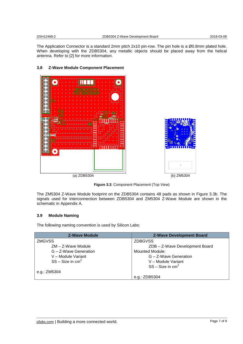
3.8 Z-Wave Module Component Placement
(a) ZDB5304 (b) ZM5304
Figure 3.3: Component Placement (Top View)
The ZM5304 Z-Wave Module footprint on the ZDB5304 contains 48 pads as shown in Figure 3.3b. The signals used for interconnection between ZDB5304 and ZM5304 Z-Wave Module are shown in the schematic in Appendix A.
3.9 Module Naming
The following naming convention is used by Silicon Labs:
Z-Wave Module Z-Wave Development Board
ZMGVSS
ZM – Z-Wave Module
G – Z-Wave Generation
V – Module Variant
SS – Size in cm2
e.g.: ZM5304
ZDBGVSS
ZDB – Z-Wave Development Board
Mounted Module:
G – Z-Wave Generation
V – Module Variant
SS – Size in cm2
e.g.: ZDB5304

DSH12468-2 ZDB5304 Z-Wave Development Board 2018-03-08
silabs.com | Building a more connected world. Page 8 of 9
4 REFERENCES
[1] DSH11243, Datasheet, “ZDP03A, Z-Wave Development Platform” [2] DSH12461, Datasheet, “ZM5304” [3] INS11681, Instruction, “500 Series Z-Wave Chip Programming Mode” [4] BOM12402, Bill of Material, ZDB5304 EU, BOM-370101680 [5] BOM12476, Bill of Material, ZDB5304 US, BOM-370101870 [6] BOM12477, Bill of Material, ZDB5304 HK, BOM-370101880

DSH12468-2 ZDB5304 Z-Wave Development Board 2018-03-08
silabs.com | Building a more connected world. Page 9 of 9
APPENDIX A SCHEMATIC

http://www.silabs.com
Silicon Laboratories Inc.400 West Cesar ChavezAustin, TX 78701USA
Smart. Connected. Energy-Friendly.
Productswww.silabs.com/products
Qualitywww.silabs.com/quality
Support and Communitycommunity.silabs.com
DisclaimerSilicon Labs intends to provide customers with the latest, accurate, and in-depth documentation of all peripherals and modules available for system and software implementers using or intending to use the Silicon Labs products. Characterization data, available modules and peripherals, memory sizes and memory addresses refer to each specific device, and "Typical" parameters provided can and do vary in different applications. Application examples described herein are for illustrative purposes only. Silicon Labs reserves the right to make changes without further notice and limitation to product information, specifications, and descriptions herein, and does not give warranties as to the accuracy or completeness of the included information. Silicon Labs shall have no liability for the consequences of use of the information supplied herein. This document does not imply or express copyright licenses granted hereunder to design or fabricate any integrated circuits. The products are not designed or authorized to be used within any Life Support System without the specific written consent of Silicon Labs. A "Life Support System" is any product or system intended to support or sustain life and/or health, which, if it fails, can be reasonably expected to result in significant personal injury or death. Silicon Labs products are not designed or authorized for military applications. Silicon Labs products shall under no circumstances be used in weapons of mass destruction including (but not limited to) nuclear, biological or chemical weapons, or missiles capable of delivering such weapons.
Trademark InformationSilicon Laboratories Inc.® , Silicon Laboratories®, Silicon Labs®, SiLabs® and the Silicon Labs logo®, Bluegiga®, Bluegiga Logo®, Clockbuilder®, CMEMS®, DSPLL®, EFM®, EFM32®, EFR, Ember®, Energy Micro, Energy Micro logo and combinations thereof, "the world’s most energy friendly microcontrollers", Ember®, EZLink®, EZRadio®, EZRadioPRO®, Gecko®, ISOmodem®, Micrium, Precision32®, ProSLIC®, Simplicity Studio®, SiPHY®, Telegesis, the Telegesis Logo®, USBXpress®, Zentri, Z-Wave and others are trademarks or registered trademarks of Silicon Labs. ARM, CORTEX, Cortex-M3 and THUMB are trademarks or registered trademarks of ARM Holdings. Keil is a registered trademark of ARM Limited. All other products or brand names mentioned herein are trademarks of their respective holders.