contents to be covered - skyupsmediablog · contents to be covered unit-i circuit concepts, rlc...
TRANSCRIPT

Contents To Be Covered
UNIT-I Circuit concepts, RLC parameters, voltage and current sources, independent and dependent
sources, source transformation, voltage-current relations for passive elements, kirchoff’s
laws , network reduction techniques, nodal analysis, mesh analysis, super nodal and super
mesh analysis.
UNIT-II RMS, average ,peak and form factor of sinusoidal wave form, steady state analysis of R,L,C
in series and parallel combinations with sinusoidal excitation,concept of reactance ,
impedance, admittance and susceptance, real,reactive and apparent powers and complex
power.
UNIT-III Locus diagrams for all series and paralle combinations of RLC parameters, resonance of
series and parallel circuits, concept of bandwidth and q factor.
Magnetic circuit, faradays laws of electro-magnetic induction, concept of self and
mutual induction, dot convention, co-efficient of coupling, composite magnetic circuit,
analysis of series and parallel magnetic circuits. UNIT-IV
Definitions, graph, tree, co-tree, cutest, tie-set, matrices for planar networks, loop and nodal
methods for analysis of networks with dependent and independent voltage and current
sources, duality and dual networks
UNIT-V Network theorems with DC and ACnexcitations,tellegen’s,compensation,thevenin’s,
nortan’s, milliman’s, reciprocity and super-position theorems.
UNIT-I 1.1 INTRODUCTION:
With increase in population the need for electricity also increases therefore it is necessary to rise
number of electrical engineers. The electrical engineering mainly deals with generation ,
transmission and distribution of electricity.
Electrical circuits is the basic and fundamental subject which lays path
to understand subjects related to generation , transmission and distribution of electricity.
In the first unit we shall deal with what is electrical circuit and formation of electrical circuit. Knowing or unknowing we come across electron in our life daily, studying the properties of these electrons leads to the terms voltage, current and power. Hence the basic definitions of voltage , current , power and energy are studied here. 1.2 CIRCUIT: The electrical circuit consists of mainly three parts , they are -- source, connecting wire and load or sink. Source : An source may be battery which forces electrons into the circuit. Connecting wire : This is part which provides path for electrons to flow. Load : The load may be bulb etc. when electrons flow through it an reaches the Source it glows . If the electrons are provided closed path to flow, leads to current is called as electrical circuit. 1.3 BASIC DEFINITIONS: Voltage(V) : The potential difference between force applied to two oppositely charged particels to bring them as near as possible is called as potential difference .( in electrical terminology it s voltage). V = W / Q (v) υ = dw / dq (v) v- volts , units of voltage.
- Unit volt is defined as 1C of charge developed when 1 J of energy is applied.
Current(I) : The flow of electrons develops the current. I = Q/ t (A) i = dq / dt (A) A = Ampere, units of current.
- Unit ampere of cuurent is constituted when 1C of charge is flowing in 1S.
Power(P): It is defined as product of volateg and power in electrical circuits or Rate of change of energy. P = dw/dt = dw/ dq . dq/dt = υ .i (W) W = watts, units of power.
Unit watt is the 1J of energy is dissipated in 1S.
Enegy : It is the capacity to do work or it is defined as power consumed over Given interval of time.(w) W = ʃ P dt.(J) J = Joules, units of energy 1J = 1 watt-sec. 1.3 BASIC PARAMETERS: Any electrical mainly consists of three important elements , they are resistor, inductor and capacitor. Let us deal these parameters in detailo. 1.3.1 Resistor: resistor is the element which restricts flow of electrons and this Property of opposing electrons is called as resistance. OHM’s Law : ohm’s law states that current flowing through circuit is Directly proportional to potential difference applied. ( at constant temperature) I α V, at constant T. I.R = V. R = V / I, hence resistance can be calculated as ratio of Volatge to current in any element or circuit. = OHMS ῼ, units of resistance. R = 1.3.2 Inductor: An length of wire twisted forms the basic inductor.(L). when Alternating curent is allowed through such a element it induces Voltage in it.
e, ɸ
Where, e = emf induced ɸ = flux developed in it for current i. Hence, e = L di/dt (v). L= is the inductance of the coil(H) H = henry units of inductance.
Unit H is the 1v of volatge induced in coil when current
changing at arte of 1A/S .
by solving above equation , current flowing through coil is given as,
i = (1/L) ʃ v dt + i(o+).
Energy stored in indcutor,
W = ʃ e.i dt = ʃ L di/dt. i dt. = (1/2) L i2
Properties:
Indcutor doesn’t allow sudden changes in current. If DC supply is provided to indcutor it acts as short circuit. Pure inductor is non-dissipative element i.e its internal resistance is zero. stores energy in the form of magnetic field.
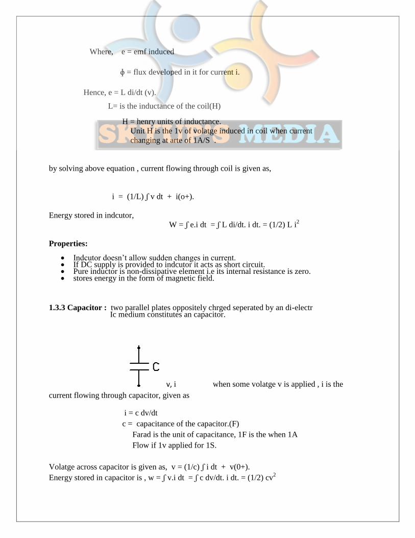
1.3.3 Capacitor : two parallel plates oppositely chrged seperated by an di-electr Ic medium constitutes an capacitor.
v, i when some volatge v is applied , i is the
current flowing through capacitor, given as
i = c dv/dt
c = capacitance of the capacitor.(F)
Farad is the unit of capacitance, 1F is the when 1A
Flow if 1v applied for 1S.
Volatge across capacitor is given as, v = (1/c) ʃ i dt + v(0+).
Energy stored in capacitor is , w = ʃ v.i dt = ʃ c dv/dt. i dt. = (1/2) cv2

Properties:
capacitor doesn’t allow sudden changes in voltage. If DC supply is provided to capacitor it acts as open circuit. Pure capacitor is non-dissipative element i.e its internal resistance is zero. stores energy in the form of electric field.
1.4 ENERGY SOURCES:
Ideal sources: These are one zero internal resistance their same will appear at
terminals .
Practical sources: These are one with internal resistance and there is a drop at
Terminal value than actual value applied.
Ideal sources Practical sources Current source : its parallel internal resistance is zero. It = Is It- terminal current Is- applied current
Current source : its parallel internal resistance is finite. It = Is – (Vs / Ri) It- terminal current Is- applied current Ri-internal resistance
Voltage source : its series internal resistance is zero. Vt = Vs Vt- terminal voltage Vs- applied voltage
Voltage source : its series internal resistance is zero. Vt = Vs – Is.Rv. Vt- terminal voltage Vs- applied voltage Rv-internal resistance
Dependent sources
Current controlled Voltage controlled
Independent sources
Ideal ( volatge and current sources) Practical( volatge and current sources)
Energy Sources
Dependent Independent

a b c d e a – volatge source b – voltage source c – current source d – voltage controlled source e – current controlled source. 1.5 TYPES OF ELEMENTS: Active and passive elements: Elements which delivers power are active and which receives power are passive. Eg: voltage and current source for active elements. R,L,C are passive elements. Uni-lataeral and bi-lateral elements: If the V-I characteristics are differenrt for different directions of current they are called as uni-lateral otherwise bi-lataeral elements. Eg: diode, transistor etc for uni-lateral elements. R for bi-lateral elements. Linear and non-linear elements: elements which obeys ohms law are called as linear otherwise non-linear. Eg: R for linear elements. L,C are non-linear elements. Lumped and distributed: Elements which are small in size are lumped and which distribuited through out the line are distributed elements Eg: cable wire for distributed elements. R,L,C in lab are lumped elements. 1.6 KIRCHOFF’S LAW: Kirchoff’s voltage law(KVL): States that algebraic sum of voltages in an loop is equal to zero.

∑ v = o. V = V1 + V2 + V3 Where, V1 = i.R1 V2 = i.R2 V3 = i.R3, from which i = V / ( R1 + R2 + R3) = Vs / Rt V = source voltage i = source current Rt = equivalent or total resistance of circuit = R1 + R2 + R3 Voltage division rule: V1 = i.R1 We know that , i = V / ( R1 + R2 + R3) = Vs / Rt Substituting i in V1, V1 = Vs / Rt * R1. Similarly, V2 = Vs / Rt * R2. V3 = Vs / Rt * R3. Kirchoff’s current law(KCL): States that sum of the current entering junction is equal to sum of the leaving the junction.
Let i1, i2 are entering currents and i3, i4 are leaving currents, then
i1+i2 = i3+i4

Vs
Current division rule:
Let Vs be the voltage at node A, I is the source current
I1 = Vs / R1
I2 = Vs / R2
Applying KCL at node A, I = I1 + I2 = Vs / R1 + Vs / R2
Vs = I. [ 1 / (1/R1) + (1/R2)] = I.Rt
Rt = [ 1 / (1/R1) + (1/R2)] = R1.R2 / (R1+R2)
I1 = I. R2/ (R1+R2).
I2 = I. R1/ (R1+R2).
1.7 NETWORK REDUCTION TECHNIQUES:
An circuit ia one with an loop , where as network is one more than one loop. An circuit is always
closed one, where as network can be either closed or opened circuited. Now let us different
techniques to solve networks.
1.7.1 Source Transformation:
To solve some of the network it may be necessary to convert voltage source to current source
and vice-versa.
Let us consider Vs is source value and its internal resistance in series is Rv across a-b terminals,
If a-b are open circuited, Voc = Vs
If a-b are short circuited, Isc = Vs / Rv

Let us consider Is is source value and its internal resistance in parallel is Ri across a-b terminals,
If a-b are open circuited, Voc = Is.Ri
If a-b are short circuited, Isc = Is
Equating above two conditions. Vs = Is.Ri
Is = Vs / Rv
From above two conditions, Is.Ri = Is. Rv
Ri = Rv
Means when source transformation is done their internal resistance will not change.
1.7.2 Star –Delta Transformations:
First figure shows elements connected in star and other elements connected in delta. Network
involved such type fo connections may be complex , hence we may require these transformation
for easy solving of networks.
In star connection,
rab = (ra + rb)
rbc = (rc + rb)
rca = (ra + rc)
In delta connection,
Rab = Ra(Rc.Rb) / (Rb+Rc)
Rbc = Rb(Rc.Ra) / (Ra+Rc)
Rca = Rc(Ra.Rb) / (Rb+Ra)
Now for transformation , rab = Rab, rbc = Rbc, rca = Rca
(ra + rb) = Ra(Rc.Rb) / (Rb+Rc) ---- 1

(rc + rb) = Rb(Rc.Ra) / (Ra+Rc) ---- 2
(ra + rc) = Rc(Ra.Rb) / (Rb+Ra) ---- 3
Delta to star transformation:
solve (1+3-2) we can find ra in terms of Ra,Rb and Rc.
ra = RaRc / (Ra+Rb+Rc)
Similarly, for rb solve (1+2-3) and rc solve (2+3-1)
rb = RaRb / (Ra+Rb+Rc)
rc = RbRc / (Ra+Rb+Rc)
Star to Delta Transformation:
Ra = ra rb+rb rc+rc ra / rc
Rb = ra rb+rb rc+rc ra / ra
Rc = ra rb+rb rc+rc ra / rb
1.7.3 MESH ANALYSIS:
Mesh analysis is an technique used to solve the complex networks consisting of more number of
meshes. Mesh analysis is nothing but applying KVL to each and every loop in circuit and solving
for mesh currents. By finding the mesh currents we can solve any require data of the network.
Let V1 = 30v, V2 = 40v, R1 =4 ohms, R2 = 2 ohms and R3 = 4 ohms

i1, i2 are the mesh currents, here positive direction of currents are assumed , but in general
we can assume current directions in any fashion and can solve.
Applying KVL to first loop we get, V1 – i1R1 – (i1+i2)R2.
V1 = (R1+R2)i1 + i2.R2. ----1
Applying KVL to second loop we get, V2 – i2R3 – (i1+i2)R2.
V2 = (R1+R2)i1 + i2.R3. ----2
Hence by solving eq. 1 and 2 we can get mesh currents i1 and i2.
Mesh analysis by inspection method:
Inspection method is direct method using mesh currents can be find directly without applying
KVL. Let us take same network as above , representing eq 1 and 2 in matrix form.
V1
V2
=
R1 R1+R2 i1
i2 R1+R2 R3
Genereally we can write in matrix form as,
V1
V2
=
R11 R12 i1
i2 R21 R22
Where, V1 – sum of all the voltage sources in 1st mesh according current flow.
V2 – sum of all the voltage sources in 2nd
mesh according current flow.
R11- self resistance of first loop, adding total resistance in 1st loop
R21= R12- mutual resistance between 1st and 2
nd loop ,
+ve if mesh currents are in same direction
-ve if mesh currents are in opposite direction
R22- self resistance of second loop, adding total resistance in 2nd
loop
1.7.4 NODAL ANALYSIS : Nodal analysis is an technique used to solve the complex networks consisting of more number
of nodes. Node analysis is nothing but applying KCL to each and every node in circuit and

solving for node voltages. By finding the node voltages we can solve any require data of the
network.
For the above circuit current division takes place at two nodes 1 and 2. Let , I3,I4,I5 are the currents flowing through R1,R2 and R3. Applying KCL at node 1, I1 = I3+I4 = Va / R1 + (Va-Vb) / R2 = Va( 1/R1 + 1/R2) - Vb / R2 ----1 Applying KCL at node 2, I2+I4 = I5 I2+(Va-Vb) / R2 = Vb / R3 I2 = - Va / R2 + Vb ( 1/R3 + 1/R2) ----2 By solving above eq.1 and 2 we can get node voltages V1 and V2. Nodal analysis by inspection method:
Inspection method is direct method using node voltages can be find directly without applying
KCL. Let us take same network as above , representing eq 1 and 2 in matrix form.
I1
I2
=
( 1/R1 +1/R2) -1/ R2 V1
V2 -1/ R2 ( 1/R3 +1/R2)
Genereally we can write in matrix form as,
I1
I2
=
G11 G12 V1
V2 G21 G22
Where, I1 – sum of all the current sources in 1st node according current flow.
I2 – sum of all the voltage sources in 2nd
node according current flow.

G11- self conductance of first node, adding total conductance in 1st node
G21= G12- mutual conductance between 1st and 2
nd loop ,
Always -ve
G22- self conductance of second node, adding total conductance in 2
nd node
1.8 CONVENTIONS:
power delivered = Vs.Is power lost = I
2 . R
volatge is positive if flow is from negative to positive called as poetntial rise.(Vs) volatge is negative if flow is from positive to negative called as poetntial drop.(I.R)
UNIT-V 5.1INTRODUCTION: Network theorems are also can be termed as network reduction techniques.Each and every
theorem got its importance of solving network. Let us see some important theorems with DC and
AC excitation with detailed procedures.
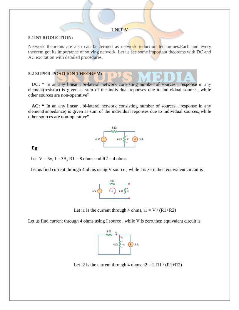
5.2 SUPER-POSITION THEOREM:
DC: “ In an any linear , bi-lateral network consisting number of sources , response in any
element(resistor) is given as sum of the individual reponses due to individual sources, while
other sources are non-operative”
AC: “ In an any linear , bi-lateral network consisting number of sources , response in any
element(impedance) is given as sum of the individual reponses due to individual sources, while
other sources are non-operative”
Eg:
Let V = 6v, I = 3A, R1 = 8 ohms and R2 = 4 ohms
Let us find current through 4 ohms using V source , while I is zero.then equivalent circuit is
Let i1 is the current through 4 ohms, i1 = V / (R1+R2)
Let us find current through 4 ohms using I source , while V is zero.then equivalent circuit is
Let i2 is the current through 4 ohms, i2 = I. R1 / (R1+R2)
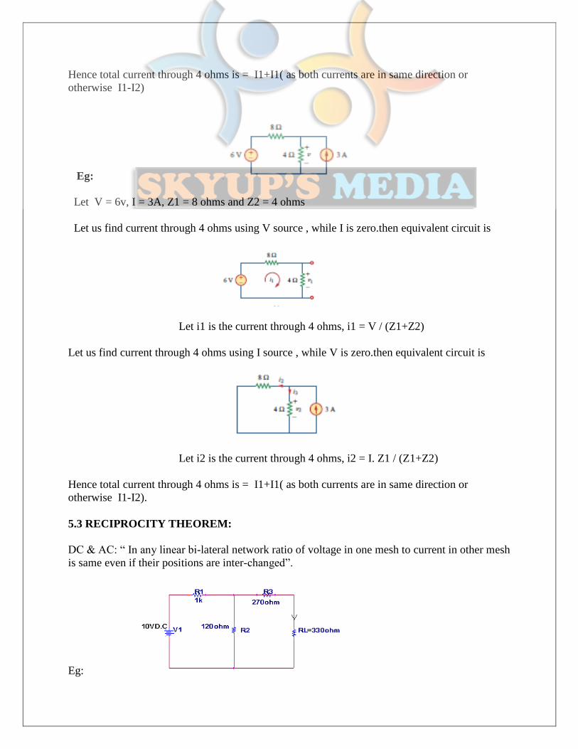
Hence total current through 4 ohms is = I1+I1( as both currents are in same direction or
otherwise I1-I2)
Eg:
Let V = 6v, I = 3A, Z1 = 8 ohms and Z2 = 4 ohms
Let us find current through 4 ohms using V source , while I is zero.then equivalent circuit is
Let i1 is the current through 4 ohms, i1 = V / (Z1+Z2)
Let us find current through 4 ohms using I source , while V is zero.then equivalent circuit is
Let i2 is the current through 4 ohms, i2 = I. Z1 / (Z1+Z2)
Hence total current through 4 ohms is = I1+I1( as both currents are in same direction or
otherwise I1-I2).
5.3 RECIPROCITY THEOREM:
DC & AC: “ In any linear bi-lateral network ratio of voltage in one mesh to current in other mesh
is same even if their positions are inter-changed”.
Eg:
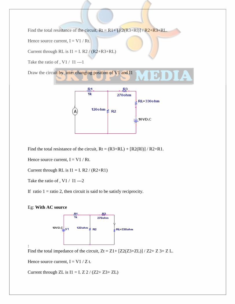
Find the total resistance of the circuit, Rt = R1+ [R2(R3+Rl)] / R2+R3+RL.
Hence source current, I = V1 / Rt.
Current through RL is I1 = I. R2 / (R2+R3+RL)
Take the ratio of , V1 / I1 ---1
Draw the circuit by inter changing position of V1 and I1
Find the total resistance of the circuit, Rt = (R3+RL) + [R2(Rl)] / R2+R1.
Hence source current, I = V1 / Rt.
Current through RL is I1 = I. R2 / (R2+R1)
Take the ratio of , V1 / I1 ---2
If ratio 1 = ratio 2, then circuit is said to be satisfy reciprocity.
Eg: With AC source
:
Find the total impedance of the circuit, Zt = Z1+ [Z2(Z3+ZL)] / Z2+ Z 3+ Z L.
Hence source current, I = V1 / Z t.
Current through ZL is I1 = I. Z 2 / (Z2+ Z3+ ZL)
Take the ratio of , V1 / I1 ---1
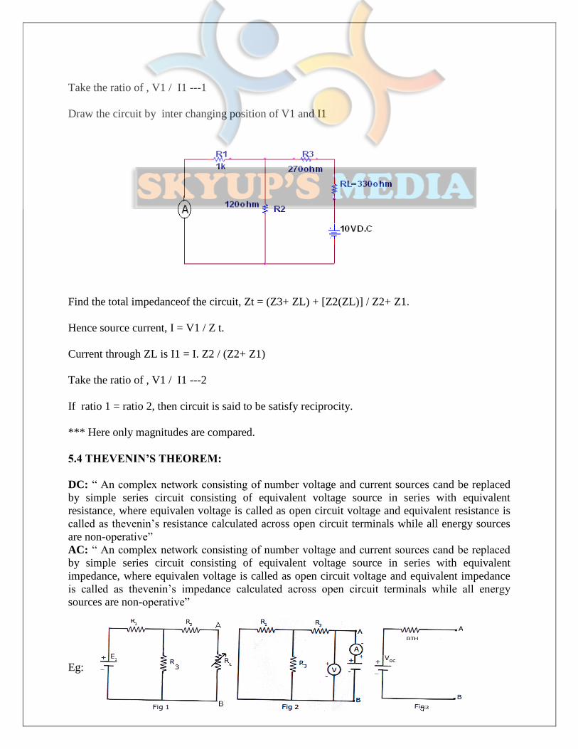
Draw the circuit by inter changing position of V1 and I1
Find the total impedanceof the circuit, Zt = (Z3+ ZL) + [Z2(ZL)] / Z2+ Z1.
Hence source current, I = V1 / Z t.
Current through ZL is I1 = I. Z2 / (Z2+ Z1)
Take the ratio of , V1 / I1 ---2
If ratio 1 = ratio 2, then circuit is said to be satisfy reciprocity.
*** Here only magnitudes are compared.
5.4 THEVENIN’S THEOREM:
DC: “ An complex network consisting of number voltage and current sources cand be replaced
by simple series circuit consisting of equivalent voltage source in series with equivalent
resistance, where equivalen voltage is called as open circuit voltage and equivalent resistance is
called as thevenin’s resistance calculated across open circuit terminals while all energy sources
are non-operative”
AC: “ An complex network consisting of number voltage and current sources cand be replaced
by simple series circuit consisting of equivalent voltage source in series with equivalent
impedance, where equivalen voltage is called as open circuit voltage and equivalent impedance
is called as thevenin’s impedance calculated across open circuit terminals while all energy
sources are non-operative”
Eg:
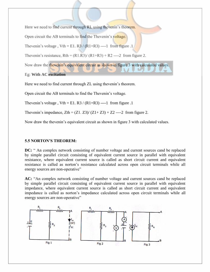
Here we need to find current through RL using thevenin’s theorem.
Open circuit the AB terminals to find the Thevenin’s voltage.
Thevenin’s voltage , Vth = E1. R3 / (R1+R3) ----1 from figure .1
Thevenin’s resistance, Rth = (R1.R3)/ (R1+R3) + R2 ----2 from figure 2.
Now draw the thevenin’s equivalent circuit as shown in figure 3 with calculated values.
Eg: With AC excitation
Here we need to find current through ZL using thevenin’s theorem.
Open circuit the AB terminals to find the Thevenin’s voltage.
Thevenin’s voltage , Vth = E1. R3 / (R1+R3) ----1 from figure .1
Thevenin’s impedance, Zth = (Z1. Z3)/ (Z1+ Z3) + Z2 ----2 from figure 2.
Now draw the thevenin’s equivalent circuit as shown in figure 3 with calculated values.
5.5 NORTON’S THEOREM:
DC: “ An complex network consisting of number voltage and current sources cand be replaced
by simple parallel circuit consisting of equivalent current source in parallel with equivalent
resistance, where equivalent current source is called as short circuit current and equivalent
resistance is called as norton’s resistance calculated across open circuit terminals while all
energy sources are non-operative”
AC: “An complex network consisting of number voltage and current sources cand be replaced
by simple parallel circuit consisting of equivalent current source in parallel with equivalent
impedance, where equivalent current source is called as short circuit current and equivalent
impedance is called as norton’s impedance calculated across open circuit terminals while all
energy sources are non-operative”

Here we need to find current through RL using norton’s theorem.
Short circuit the AB terminals to find the norton’s current.
Total resistance of circuit is, Rt = (R2.R3) / (R2+R3) + R1
Source current, I = E / Rt
Norton’s current , IN = I. R3 / (R2+R3) ----1 from figure .1
Norton’s resistance, RN = (R1.R3)/ (R1+R3) + R2 ----2 from figure 2.
Now draw the Norton’s equivalent circuit as shown in figure 3 with calculated values.
Eg: With AC excitation
Here we need to find current through ZL using norton’s theorem.
Short circuit the AB terminals to find the norton’s current.
Total impedance of circuit is, Zt = (Z2. Z3) / (Z2+Z3) + Z1
Source current, I = E / Zt
Norton’s current , IN = I. Z3 / (Z2+Z3) ----1 from figure .1
Norton’s impedance, ZN = (Z1. Z3)/ (Z1+Z3) + Z2 ----2 from figure 2.
Now draw the Norton’s equivalent circuit as shown in figure 3 with calculated values.
*** These two theorems are useful in determining the load value for which maximum power
transfer can be happened.
5.6 MAXIMUM POWER TRANSFER THEOREM:
DC: “ In linear bi-lateral network maximum power can be transferred from source to load if load
resistance is equal to source or thevenin’s or internal resistances”.
AC: “ In linear bi-lateral network maximum power can be transferred from source to load if load
impedance is equal to complex conjugate of source or thevenin’s or internal impedances”
Eg: For the below circuit explain maximum power transfer theorem.
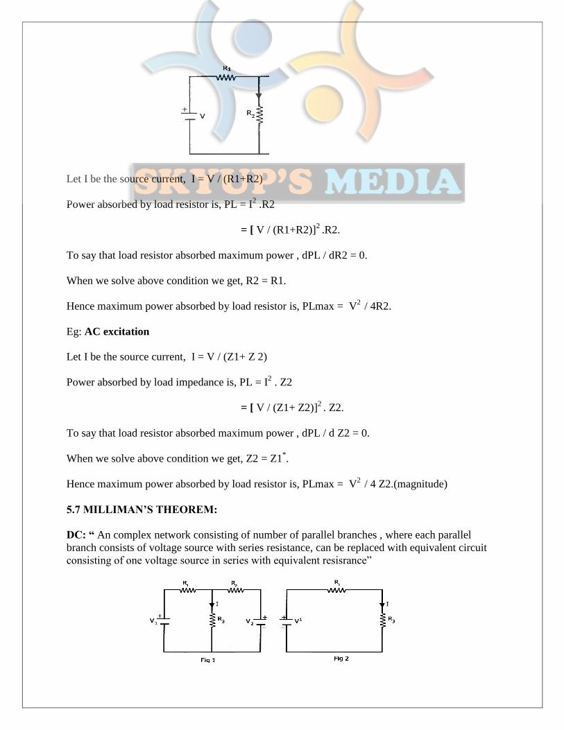
Let I be the source current, I = V / (R1+R2)
Power absorbed by load resistor is, PL = I2 .R2
= [ V / (R1+R2)]2
.R2.
To say that load resistor absorbed maximum power , dPL / dR2 = 0.
When we solve above condition we get, R2 = R1.
Hence maximum power absorbed by load resistor is, PLmax = V2
/ 4R2.
Eg: AC excitation
Let I be the source current, I = V / (Z1+ Z 2)
Power absorbed by load impedance is, PL = I2 . Z2
= [ V / (Z1+ Z2)]2
. Z2.
To say that load resistor absorbed maximum power , dPL / d Z2 = 0.
When we solve above condition we get, Z2 = Z1*.
Hence maximum power absorbed by load resistor is, PLmax = V2
/ 4 Z2.(magnitude)
5.7 MILLIMAN’S THEOREM:
DC: “ An complex network consisting of number of parallel branches , where each parallel
branch consists of voltage source with series resistance, can be replaced with equivalent circuit
consisting of one voltage source in series with equivalent resisrance”

Where equivalent voltage source value is , V’ = (V1G1+V2G2+------+VnGn)
--------------------------------
G1+G2+----------------Gn
Equivalent resistance is , R’ = 1 / ( G1+G2+-------------------Gn)
AC: “ An complex network consisting of number of parallel branches , where each parallel
branch consists of voltage source with series impedance, can be replaced with equivalent circuit
consisting of one voltage source in series with equivalent impedance”
Where equivalent voltage source value is , V’ = (V1Y1+V2Y2+------+VnYn)
--------------------------------
Y1+Y2+----------------Yn
Equivalent resistance is , Z’ = 1 / ( Y1+Y2+-------------------Yn)
*** It is also useful in designing load value for which it absorbs maximum power.
5.8 COMPENSATION THEOREM:
DC &AC: “ compensation theorem states that any element in the network can be replaced with
Voltage source whose value is product of current through that element and its value”
It is useful in finding change in current when sudden change in resistance value.
For the above circuit source current is given as, I = V / (R1+R2)
Element R2 can be replaced with voltage source of ,V’ = I.R2
Let us assume there is change in R2 by ΔR, now source current is I’= V / (R1+R2+ ΔR)
Hence actual change in current from original circuit to present circuit is = I – I’.
This can be find using compensation theorem as, making voltage source non-operative and
replacing ΔR with voltage source of I’. ΔR.
Then change in current is given as = I’. ΔR / (R1+R2)

UNIT-IV
4.1 NETWORK TOPOLOGY:
Network topology is the one of the technique to solve electrical networks consisting of number
og meshes or number of nodes,where it is difficult to apply mesh and nodal analysis.
Graph theory is the technique where all the elements of the network are
Represented by straight lines irrespective of their behaviour. Here matrix methods are used to
solve complex networks. Before seeing the actual matrices , the knowledge of some of the
definitions is very important. They are---
4.2 DEFINITONS:
Node : An node is junction where two or more than two elements are connected.
Degree of the node: number of elements connected to the node is defined as degree of the node.
Branch: An branch is a element(s) connected between pair of nodes.
Path: It is traversal of signal between pair of nodes.
Loop: It is the path started from an node and ends at the same node.
Graph: An graph is formed when all the elements of the network are replaced by straight line
irrespective of their behaviour.
Oriented and non-oriented graph: If the graph of the network is represented with directions in
each and every branch then it is oriented, if atleast one branch of graph has no direction then iti is
non-oriented graph.
Planar and non-planar graph: if an graph can be on plane surface without cross over then
system is planar and vise-versa is non-linear.
Tree: Tree is the sub-graph of the graph , which consists of same number of nodes as that of
original graph without any closed path.
Branches of the tree are called as twigs. Number of possible twigs in an tree are (n - 1).
n – number of nodes
Co-tree: The set of braches which are removed to form tree are called as co-tree.

Links: Branches removed to form tree are called as links.
l = b – (n-1)
4.3 INCIDENCE MATRIX(A):
Incidence matrix is formed between number of nodes and number of branches. This matrix is
useful easy understanding of network and any complex network can be easily feed into system
for coding. Order of incidence matrix is (n*b)
Procedure to incidence matrix:
aij = 1, if jth branch is incidence to ith node and direction is away from node.
aij = -1, if jth branch is incidence to ith node and direction is towards from node.
aij = 0, if jth branch is not incidence to ith node .
Properties of incidence matrix:
1. Number of non zero entries of row indicates degree of the node.
2. The non zero entries of the coloumn represents branch connections.
3. If two coloumns has same entries then they are in parallel.
Reduced incidence matrix:
Reduced incidence matrix is formed by eliminating one of the row from incidence matrix
generally ground node row is eliminating, which is representing by A!. Number of possible trees
of for any graph are det(A! A!T).
Once we form the incidence matrix , we can write KCL equations any complex without appling
KCL as follows,
A!.Ib = 0
Where, A! - reduced incidence matrix
Ib - branch current matrix( an coloumn matrix)
4.4 TIE-SET MATRIX:
Tie-set matrix is formed between link currents and branch currents. The order of tie-set matrix is
(Il*Ib). it is represented by B. Tie-set is defined as a loop which consists of one link any number
of branches. Hence total number of tie-set possible with above definition are number of links.

Procedure to form tie-set matrix:
Bij = 1, if current direction of jth branch coincides with direction of ith link.
Bij = -1, if current direction of jth branch opposes with direction of ith link.
Bij = 0, if jth branch has no relation with ith link.
Once we form tie-set matrix KVL equations of any complex network can be written as B.Vb = 0
Where, B = tie-set matrix
Vb = branch voltage matrix(coloumn matrix)
From the knowledge of tie-set matrix we can calculate all the branch currents in terms of link
currents, which is given as
Ib = BT . Il
Where, Ib - branch current matrix( an coloumn matrix)
Il - link current matrix( an coloumn matrix)
BT- transpose of tie-set matrix
4.5 CUT-SET MATRIX:
Cut-set matrix is formed between twig voltages and branch voltages. The order of cut-set matrix
is ((n-1)*b). it is represented by C. Cut-set is defined as minimum set of branches by removing
which graph is divided into two sub-graphs, where one of the part is an isolated node. Hence
total number of cut-set possible with above definition are number of twigs. Generally cut-set
direction is assumed in direction of branch, as cut-set consists of one branch any number of links.
Procedure to form tie-set matrix:
cij = 1, if direction of jth branch coincides with direction of ith cut-set.
cij = -1, if direction of jth branch opposes with direction of ith cut-set.
cij = 0, if direction of jth branch is not in the ith cut-set.
Once we form cut-set matrix KCL equations of any complex network can be written as C.Ib = 0
Where, C= cut-set matrix
Ib = branch current matrix(coloumn matrix)
From the knowledge of cut-set matrix we can calculate all the branch voltages in terms of twig
voltages, which is given as
Vt = CT . Vb
Where, Vb - branch voltage matrix( an coloumn matrix)
Vt – twig voltage matrix( an coloumn matrix)
CT- transpose of cut-set matrix
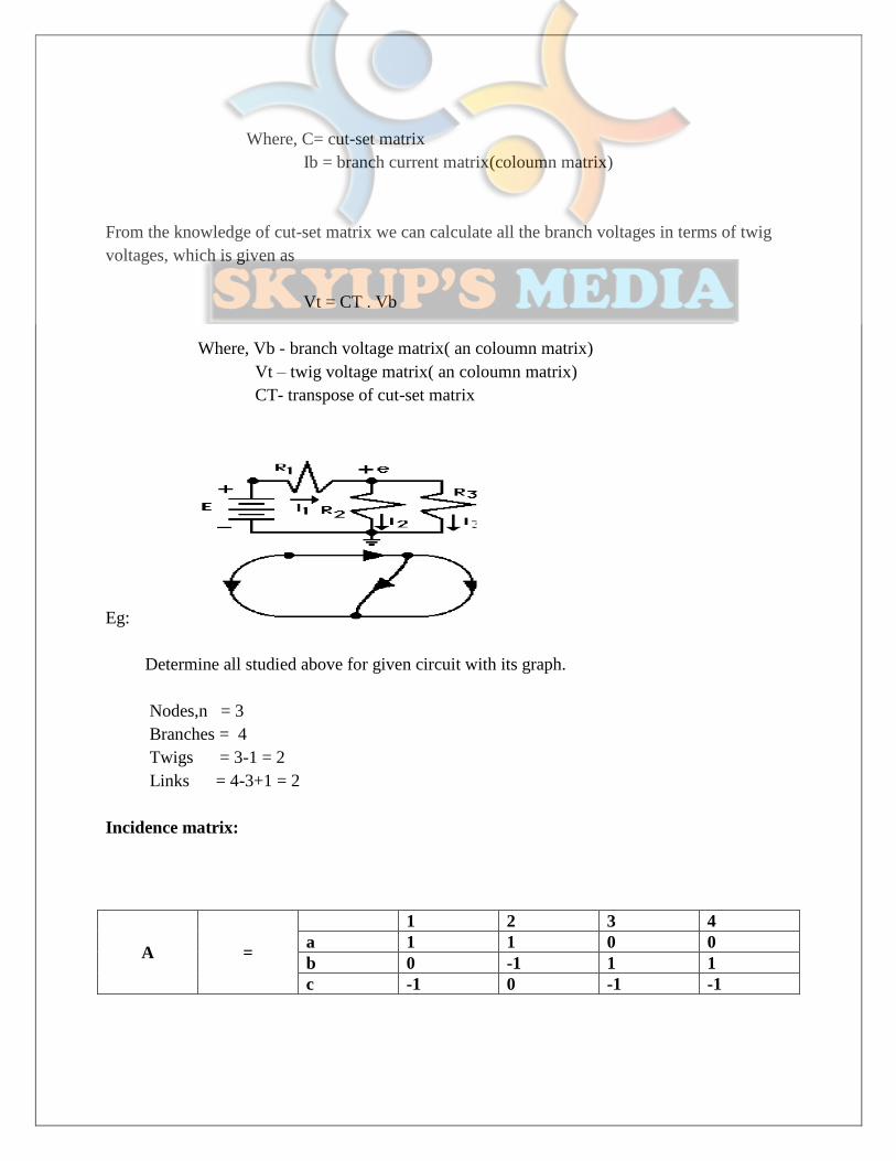
Eg:
Determine all studied above for given circuit with its graph.
Nodes,n = 3
Branches = 4
Twigs = 3-1 = 2
Links = 4-3+1 = 2
Incidence matrix:
A =
1 2 3 4
a 1 1 0 0
b 0 -1 1 1
c -1 0 -1 -1

Reduced Incidence matrix:
A! =
1 2 3 4
a 1 1 0 0
b 0 -1 1 1
Tie-set matrix:
As tree can be formed with two branches remaining two are links, let 2,4 arethe links.
B =
i1 i2 i3 i4
i2 -1 1 1 0
i4 0 0 -1 1
We can write all branch currents as, Ib = BT . Il
i1
=
-1 0 i2
i2 1 0
i3 1 -1 i4
i4 0 1
Hence , i1 = -i2
i2 = i2
i3 = i2-i4
i4 = i4
Cut-set matrix:
Let the two cut-set are (1,2) and (2,3,4) as possible cut-sets are (n-1) = (3-1) =2.
Here 1 and 3 are branches or twigs hence cutsets direction is same as these branch directions.
C =
1 2 3 4
C(1,2) 1 -1 0 0
C(2,3,4) 0 -1 1 1

We can write all branch voltages as, Vb = CT . Vt
V1
=
1 0 V1
V2 -1 -1
V3 0 1 V3
V4 0 1
Hence, V1 = V1
V2 = -V1-V3
V3= V3
V4 = V3
4.6 DUAL AND DUALITY:
Some times for easy simplification of network we may need dual network of original network.
Dual network is formed by using dual parameters.
Dual parameters:
Series Parallel
Parallel Series
Voltage Current
Current Voltage
Resistance Conductance
Inductance capacitance
Capacitance Inductance
Open Short
Short open
Procedure to draw dual network for original network:
1. Firstly assume node in each an every loop and node outside the circuit.
2. Now replace the element which purely belongs to respective loop with its dual element
between node assumed in that loop and node outside loop.
3. Now replace the element which belongs two loops with its dual element between node
assumed in that loop and node assumed in other loop.
*** Even we draw the dual network for original network the behaviour of network willnot
change.

UNIT-III
3.1 MAGNETIC CIRCUITS
Let us consider an coil allowing current of IA which develops magnetic lines of force forming
north and south poles , the flow of magnetic lines from north pole to south pole. If coil is
wounded on some core allowing current IA develops flux Ф and this flux follows the path of
core to form magnetic circuit.
3.2 Definitions:
Magnetic flux density: Flux developed per unit area. (Ф / A). Represented with B.
Whose units are webers/mt2 or tesla.
MMF( Magneto motive force): It is the measure of ability of amount of flux can be developed in
the coil.(J), which is given as product of number of turns and
current flowing through coil.
J = N.I (A-turns)
Field intensity: It is defined as mmf per unit length.(H)
H = mmf / l ( A-turns / mt)
Reluctance: It is the property of core which opposes magnetic flux. Generally cores of two types
,they are air and iron core. When compare to iron core air core has more reluctance
Property.
(or)
Reluctance is ratio of mmf to the flux.( J / Ф)
R = (l / µ.A) .
Where, l – mean length of magnetic circuit.
A – area of cross of core.
µ - permeability of the core.
- µo. µr
- absolute permeability(µo)
- relative permeability(µr)—varies for different types of cores.
Hence mmf is also given as ,J = R. Ф

Fringing and leakage effect:
Let us consider ring core with small air gap. When flux developed in core, during flow of flux if
there is a sudden change in core whose values are largely differ , flux suddenly bulges out which
is called as fringing.
Generally core laminated and these lamination may consists of some weak points and flux leaked
through these weak points is called as leakage flux.
3.3 Series magnetic circuit:
Let us consider an coil of N turns wounded on ring core. When some current I A is allowed
through coil flux Ф is developed in it.
Let, mmf required to develop Ф is J
R is reluctance of core.
N- number of turns.
I- Current through coil.
Hence , mmf, J = N.I
Drop in core is = Ф.R
J = Ф.R = N.I
Therefore flux developed in coil is given as, Ф = N.I / R
3.4 Composite magnetic circuit:
Let us consider ring core which comprises of three different materials with different lengths and
areas. An coil of N turns is wounded on such core as described above, allowing current I A.
Let , Ф1 = flux developed in the first part of core
R1 = reluctance of first part of the core
l1 = length of first part of the core
A1 = area of first part of core
J1 = mmf drop in first part of core

Ф2 = flux developed in the 2nd part of core
R2 = reluctance of 2nd part of the core
l2= length of 2nd part of the core
A2 = area of 2nd part of core
J2= mmf drop in 2nd part of core
Ф3 = flux developed in the 3rd
part of core
R3= reluctance of 3rd
part of the core
l3= length of 3rd
part of the core
A3 = area of 3rd
part of core
J3 mmf drop in 3rd
part of core
Hence total mmf required, J = J1+J2+J3
= Ф1.R1+ Ф2.R2+ Ф3.R3=N.I
Total flux developed is = NI / (R1+R2+R3)
Where , R1 = (l1 / µ1.A1)
R2 = (l2 / µ2.A2)
R3 = (l3 / µ3.A3)
3.5 Coupled circuits:
When two coils are brought together as close as possible then they form coupled coils.
Here when current(i1) is allowed through first coil then magnetic flux Ф1 is developed in it, as
other coil brought to close proximity some of Ф1 links with second coil called as Фm1 their by
inducing voltage in it and when we close the second coil current flows in it (i2). This current i2
develops Ф2 in it and some of Ф2 links with 1st coil called as Фm2. If the two coils are of same
dimensions Фm1= Фm2= Фm.
Here we define two inducatnces slef inductance of coils L1 and L2, mutal inductance between
the coils M12=M21=M. Now we can say that total emf induced in coil is the combination of self
and mutually induced emf.

Emf in 1st coil , v1= L1 di1/dt + Mdi2/dt
Emf in 2nd
coil , v2= L2 di2/dt + Mdi1/dt
3.5.1 Types of coupled coils:
Coupled coils are of three types, they are
1. Conductively coupled: Here an voltage is fed to the potential divider circuit
Called as conductively coupled
2. Inductively coupled: where there is no electrical cconnection, i.e electrically
Isolated but magnetically coupled.
Eg: Transformer .
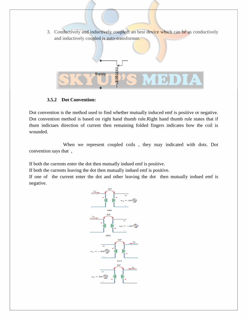
3. Conductively and inductively coupled: an best device which can be as conductively
and inductively coupled is auto-transformer.
3.5.2 Dot Convention:
Dot convention is the method used to find whether mutually induced emf is positive or negative.
Dot convention method is based on right hand thumb rule.Right hand thumb rule states that if
thum indictaes direction of current then remaining folded fingers indicates how the coil is
wounded.
When we represent coupled coils , they may indicated with dots. Dot
convention says that ,
If both the currents enter the dot then mutually indued emf is positive.
If both the currents leaving the dot then mutually indued emf is positive.
If one of the current enter the dot and other leaving the dot then mutually indued emf is
negative.
3.5.3 co-efficient of coupling:
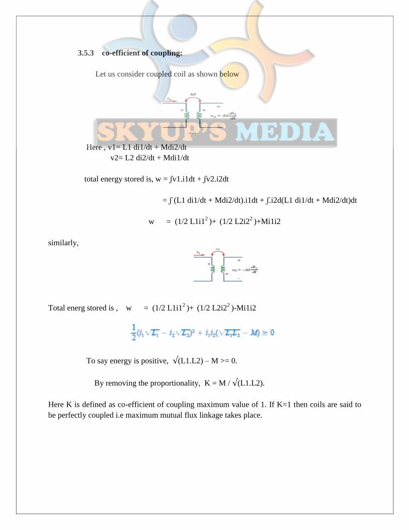
Let us consider coupled coil as shown below
Here , v1= L1 di1/dt + Mdi2/dt
v2= L2 di2/dt + Mdi1/dt
total energy stored is, w = ʃv1.i1dt + ʃv2.i2dt
= ʃ (L1 di1/dt + Mdi2/dt).i1dt + ʃ.i2d(L1 di1/dt + Mdi2/dt)dt
w = (1/2 L1i12
)+ (1/2 L2i2
2 )+Mi1i2
similarly,
Total energ stored is , w = (1/2 L1i12
)+ (1/2 L2i2
2 )-Mi1i2
To say energy is positive, (L1.L2) – M >= 0.
By removing the proportionality, K = M / (L1.L2).
Here K is defined as co-efficient of coupling maximum value of 1. If K=1 then coils are said to
be perfectly coupled i.e maximum mutual flux linkage takes place.

3.6 RESONANCE:
If an electriacl circuit offers impedance which is purely resistive then it is said to
be uder resonance and frequency of the circuit at which it happens is called as
resonant frequency. While studying the resonance of electrical circuits we
unedrstand terms like resonant frequency, bandwidth, cut-off frequencies and
quality factor.
Resonant frequency:
It is the frequency at which maximum response occurs or net impedance is purely
resistive or minimum impedance is offered by circuit.(fr)
Bandwidth:
It is the range of frequencies within which signal can be esily transmitted with out
any overlap of other signals. It is also given as difference between
Higher cutt-off frequency and lower cutt-off frequency.(Bw = fh - fl)
Cutt-off frequencies:
It is the frequency at which response of the circuit is the 70.7% of maximum value
or 0.707 of maximum value. This can be happen at two frequencies called as
lower cutt-off frequencies < fr and higher cutt-off frequencies < fr.
Quality factor:
Quality factor is the measurement of quality of the energy storing elements ,
which in turn indictaes life time of energ storing elements.
Q = 2Π * energy stored in the element
----------------------------------
Energy dissipated in one cycle.
3.6.1 Types of resonance:
Depending on types of circuit resonance is defined. The are
1. Series resonance: series is related to series RLC circuit. In an series RLC circuit
resonance occurs when voltage across L and C are same in magnitude and 180 degrees
out of phase.
2. Parallel resonance: series is related to Parallel RLC circuit. In an Parallel RLC circuit
resonance occurs when current flowing through L and C are same in magnitude and 180
degrees out of phase.
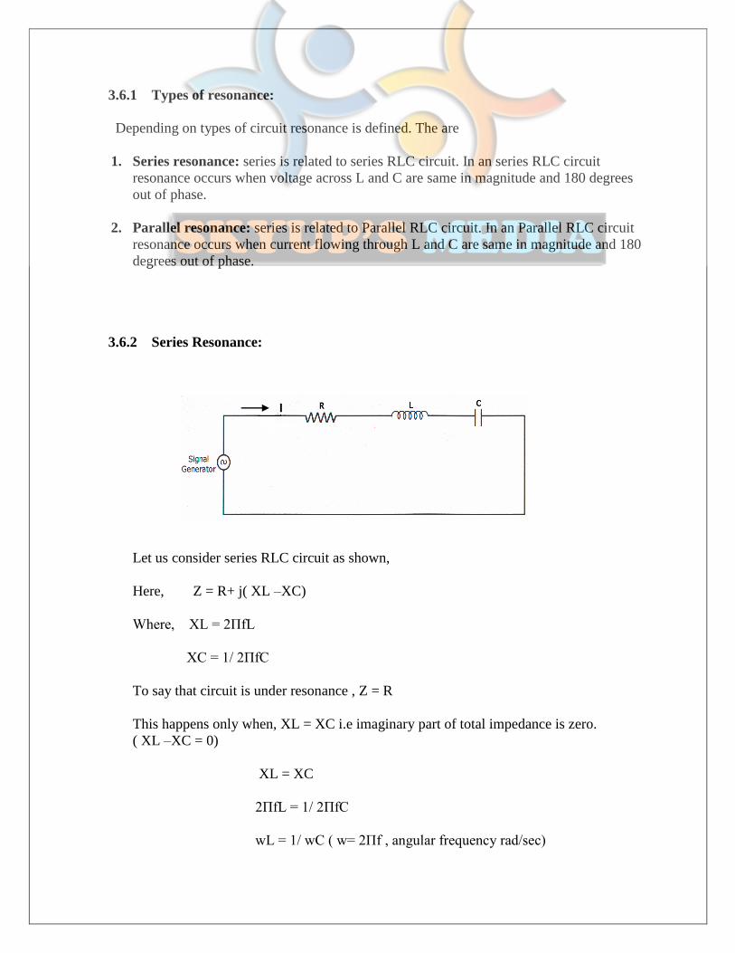
3.6.2 Series Resonance:
Let us consider series RLC circuit as shown,
Here, Z = R+ j( XL –XC)
Where, XL = 2ΠfL
XC = 1/ 2ΠfC
To say that circuit is under resonance , Z = R
This happens only when, XL = XC i.e imaginary part of total impedance is zero.
( XL –XC = 0)
XL = XC
2ΠfL = 1/ 2ΠfC
wL = 1/ wC ( w= 2Πf , angular frequency rad/sec)
I
w2 = 1/
fr = 1/ 2Π --- resonant frequency.
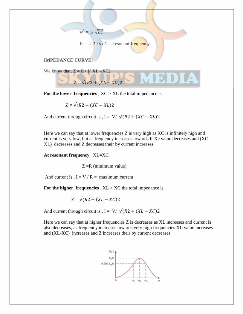
IMPEDANCE CURVE:
We know that, Z = R+ j( XL –XC)
Z =
For the lower frequencies , XC > XL the total impedance is
Z =
And current through circuit is , I = V/
Here we can say that at lower frequencies Z is very high as XC is infinitely high and
current is very low, but as frequency increases towards fr Xc value decreases and (XC-
XL) decreases and Z decreases their by current increases.
At resonant frequency, XL=XC
Z =R (minimum value)
And current is , I = V / R = maximum current
For the higher frequencies , XL > XC the total impedance is
Z =
And current through circuit is , I = V/
Here we can say that at higher frequencies Z is decreases as XL increases and current is
also decreases, as frequency increases towards very high frequencies XL value increases
and (XL-XC) increases and Z increases their by current decreases.

Here for frequencies < fr circuit is said to be dominantly capacitive and for frequencies >
fr circuit is said to be dominantly inductive.
BANDWIDTH :
Let f1 , f2 --- lower and higher cut-off frequencies
At f1, I = V /
And also at f2, I = V /
This is possible only when ,
At f1 , 1/ w1 C – w1. L = R ----1
f2, w2 L – 1/w2. C = R ----2
equate 1 and 2
1/ w1 C – w1. L = w2 L – 1/w2. C
1/ w1 C – w1. L = w2 L – 1/w2. C
w1.w2 = 1/ LC
w1.w2 = wr2
now add two equations,
1/ w1 C – w1. L + w2 L – 1/w2. C =2R
(w2-w1)L + (w2-w1)/w1w2C = 2R
By sloving above equation, f2 – f1 = R / 2ΠL
Lower cut off frequency (f1) = fr-R/4∏L
Upper cut off frequency (f2) = fr+R/4∏L

Quality factor: For inductor.
Q = 2Π * energy stored in the element
----------------------------------
Energy dissipated in one cycle.
Q = 2Π * ½ LI2
-------------
I2.
R.t
Q = 2Π * ½ LI2
-------------
I2.
R.1/f
Q = 2ΠL /R = XL /R
For capacitor.
Q = 2Π * energy stored in the element
----------------------------------
Energy dissipated in one cycle.
Q = 2Π * ½ CV2
-------------
I2.
R.t
Q = 2Π * ½ CV2
-------------
(V/ )2.
R.1/f
Q = 1 /2Π fC R = XC /R

MAGNIFICATION:
Magnification is defined ratio voltage across energy storing elements and input voltage under
resonance.
VL / Vi = IXL / IR = XL / R =Q
VC / Vi = IXC / IR = XC / R =Q
To say that life of the circuit is high the magnification must be high.
3.6.3 Parallel Resonance:
Let us consider parallel RLC circuit as shown,
Here, Y =1/ R+ j( 1/XL –1/XC) = G+ j(BL – BC)
Where, BL = 1 / 2ΠfL
BC = 2ΠfC
To say that circuit is under resonance , Y = G
This happens only when, BL = BC i.e imaginary part of total impedance is zero.
( BL –BC = 0)
BL = BC
Signal
Generator

1 / 2ΠfL = 2ΠfC
1 / wL = wC ( w= 2Πf , angular frequency rad/sec)
w2 = 1/
fr = 1/ 2Π --- resonant frequency.
ADMITTANCE CURVE:
We know that, Y = G+ j(BL – BC)
Y =
For the lower frequencies , BL > BC the total admittance is
Y =
And current through circuit is , V = I /
Here we can say that at lower frequencies Y is very high as BL is infinitely high and
voltage is very low, but as frequency increases towards fr BL value decreases and (BL-
BC) decreases and Y decreases their by voltage increases.
At resonant frequency, BL=BC
Y =1 / R (minimum value)
And voltage is , V = I / G = maximum current
For the higher frequencies , BC > BL the total admittance is
Y =
And current through circuit is , V = I/
Here we can say that at higher frequencies Y is decreases as BC increases and voltage is
also decreases, as frequency increases towards very high frequencies BC value increases
and (BC-BL) increases and Y increases their by voltage decreases.

Here for frequencies < fr circuit is said to be dominantly inductive and for frequencies >
fr circuit is said to be dominantly capacitive.
BANDWIDTH :
Let f1 , f2 --- lower and higher cut-off frequencies
At f1, V = I /
And also at f2, V = I /
This is possible only when ,
At f1 , w1 C – 1/w1. L = G ----1
f2, 1 / w2 L – w2. C = G ----2
equate 1 and 2
1w1 C – 1 / w1. L = 1 / w2 L – w2. C
1/ w1 C – w1. L = w2 L – 1/w2. C
w1.w2 = 1/ LC
w1.w2 = wr2
now add two equations,
w1 C – 1 / w1. L + 1 / w2 L – w2. C =2G
By sloving above equation, f2 – f1 = 1 / 2ΠRC
Lower cut off frequency (f1) =fr-1/4∏RC
Upper cut off frequency (f2) = fr+1/4∏RC
Quality factor: For inductor.
Q = 2Π * energy stored in the element
----------------------------------
Energy dissipated in one cycle.
Q = 2Π * ½ L(V/XL)2
-------------
(V / R)2.
.t
Q = 2Π * ½ LI2
-------------
I2.
R.1/f
Q = R / XL
For capacitor.
Q = 2Π * energy stored in the element
----------------------------------
Energy dissipated in one cycle.
Q = 2Π * ½ CV2
-------------
I2.
R.t
Q = 2Π * ½ CV2
-------------
(V/ )2.
R.1/f
Q = R / BC = XC.R

MAGNIFICATION:
Magnification is defined ratio voltage across energy storing elements and input voltage under
resonance.
IL / I = V/BL / V/R = R / BL
IC / Ii = V / BC / V / R = R / BC =Q
To say that life of the circuit is high the magnification must be high.
3.7 LOCUS DIAGRAM:
Locus diagram is the graphical representation of response of the circuit by varying any one
of the parameter in the circuit while others are kept fixed. Locus diagram is draw for current of
the circuit with its phase. Locus diagram can be drawn for series RL, RC and RLC, similarly for
parallel RL,RC and RLC
UNIT –II
2.1 INTRODUCTION:
The alternating quantity is one whose value varies with time. This alternating quantity may
be periodic and non-periodic. Periodic quantity are one whose value will be repeated for every
specified interval . Generally to represent alternating voltage or current we prefer sinusoidal
wave form , because below listed properties—
1. Derivative of sine is an sine function only.
2. Integral of sine is an sine function only.
3. It is easy to generate sine function using generators.
4. Most of the 2nd
order system response is always sinusoidal.
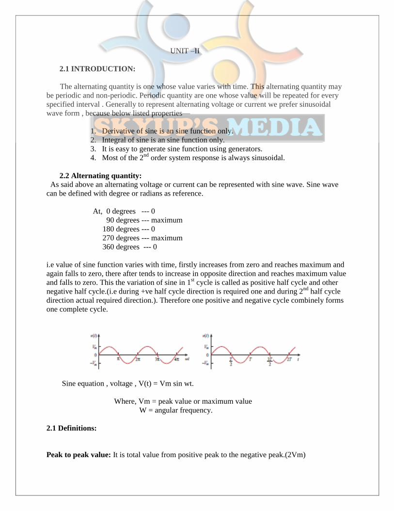
2.2 Alternating quantity:
As said above an alternating voltage or current can be represented with sine wave. Sine wave
can be defined with degree or radians as reference.
At, 0 degrees --- 0
90 degrees --- maximum
180 degrees --- 0
270 degrees --- maximum
360 degrees --- 0
i.e value of sine function varies with time, firstly increases from zero and reaches maximum and
again falls to zero, there after tends to increase in opposite direction and reaches maximum value
and falls to zero. This the variation of sine in 1st cycle is called as positive half cycle and other
negative half cycle.(i.e during +ve half cycle direction is required one and during 2nd
half cycle
direction actual required direction.). Therefore one positive and negative cycle combinely forms
one complete cycle.
Sine equation , voltage , V(t) = Vm sin wt.
Where, Vm = peak value or maximum value
W = angular frequency.
2.1 Definitions:
Peak to peak value: It is total value from positive peak to the negative peak.(2Vm)
Instantaneous value: It is the magnitude of wave form at any specified time. V(t)
Average value : It is ratio of area covered by wave form to its length.(Vd)
Vd = (1/T) ʃ V(t) dwt.
Vd = (1 / 2Π) ʃ Vm sin wt.dwt
= - Vm / 2Π . coswt---with limits of 2Π and 0
= 0.( i.e average value of sine wave over a full cycle is zero)
Hence it is defined for half cycle.
Vd = (1 / Π) ʃ Vm sin wt.dwt
= - Vm / Π . coswt---with limits of Π and 0
= 2Vm / Π
RMS value:
It is the root mean square value of the function, which given as
Vrms = (1/T) ʃ V(t)]2 dwt.
= (1/2Π) ʃ Vm2[ (1- cos2wt)/2]dwt.
= (1/2Π) .Vm2[ (wt- sin2wt / 2wt)/2]
= Vm / = effective value.
Peak factor:
It is the ratio of peak value to the rms value.
Pp = Vp / Vrms =
Form factor:
It is the ratio of average value to the rms value.
Fp = Vd / Vrms = 2 / Π = 1.11
Eg: Find the peak, peak to peak, average, rms, peak factor and form factor of given current
function , i(t) = 5 sin wt.
2.2 Phase and phase difference:
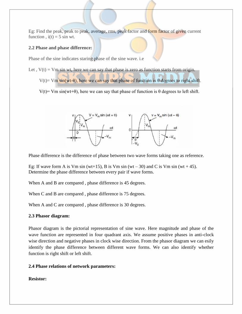
Phase of the sine indicates staring phase of the sine wave. i.e
Let , V(t) = Vm sin wt, here we can say that phase is zero as function starts from origin.
V(t)= Vm sin(wt-θ), here we can say that phase of function is θ degrees to right shift.
V(t)= Vm sin(wt+θ), here we can say that phase of function is θ degrees to left shift.
Phase difference is the difference of phase between two wave forms taking one as reference.
Eg: If wave form A is Vm sin (wt+15), B is Vm sin (wt – 30) and C is Vm sin (wt + 45).
Determine the phase difference between every pair if wave forms.
When A and B are compared , phase difference is 45 degrees.
When C and B are compared , phase difference is 75 degrees.
When A and C are compared , phase difference is 30 degrees.
2.3 Phasor diagram:
Phasor diagram is the pictorial representation of sine wave. Here magnitude and phase of the
wave function are represented in four quadrant axis. We assume positive phases in anti-clock
wise direction and negative phases in clock wise direction. From the phasor diagram we can esily
identify the phase difference between different wave forms. We can also identify whether
function is right shift or left shift.
2.4 Phase relations of network parameters:
Resistor:

Let us consider resistor allowing alternating current i(t). then the voltage drop across resistor is
given as,
If, V(t) = Vm sin wt
V(t) = i(t).R
i(t) = V(t) / R
= Vm sin wt / R
i(t) = Im sin wt.
The ratio of V(t) / i(t) = Z = impedance offered by resistor.(ohms).
Z = Vm sin wt / Im sin wt.
= Vm / Im
Hence we can say that V(t) and i(t) in resistor element are in phase.
Inductor:
Let us consider an coil of N turns allowing current i(t).( Im sin wt)
Hence emf induced in the coil is ,
V(t) = L di(t) / dt
= L d(Im sin wt) / dt
= L w Im coswt
= Vm coswt = Vm sin(wt + 90).
Where, Vm = L w Im = Im .XL
XL = reactance offered by coil.
Impedance offered by coil is , Z = V(t) / i(t)

= Vm sin(wt + 90) / Im sin wt
The function Vm sinwt = Vm .
Z = Vm / Im
Z = Vm / Im
= j wL = j XL ( j = 1 )
As there is left shift in V(t), we can say that i(t) lags V(t) by 90 degrees.
Capacitor:
Let us consider an capacitor allowing current i(t).( Im sin wt)
Hence voltage across it is ,
V(t) = 1 / C ∫ i(t) dt
= 1 / C ∫ Im sin wt dt
= - coswt .Im / wC
= = Vm sin(wt - 90).
Where, Vm = Im/ wC = Im .XC
XC = reactance offered by capacitor
Impedance offered by capacitor is , Z = V(t) / i(t)
= Vm sin(wt -90) / Im sin wt
The function Vm sinwt = Vm .
Z = Vm / Im
Z = Vm / Im

= -j wL =- j XL ( j = 1 )
As there is right shift in V(t), we can say that i(t) leads V(t) by 90 degrees.
2.5 Power in Ac circuits:
In the case of DC circuits power is given as product of voltage and current in that element.
P = V.I (W)
Let V(t) = Vm sin wt
i(t) = Im sin(wt +90)
instantaneous power , P(t) = V(t).i(t)
= Vm sin wt. Im sin(wt + Ф)
= Vm.Im sin wt sin (wt + Ф).
= Vm.Im 2. sin wt sin (wt + Ф).
--------------------------------
2
= Vm.Im 2. sin wt sin (wt + Ф).
--------------------------------
.
= Vm.Im [ cos Ф – cos( 2wt + Ф)]
--------------------------------
.
Average power , Pav = 1/ 2π ∫ p(t) dwt.
= 1/ 2π ∫ Vm.Im [ cos Ф – cos( 2wt + Ф)] dwt

--------------------------------
.
As average value over full cycle is equal to zero, hence second term can be neglected.
Pav = 1/ 2π ∫ Vm.Im [ cos Ф ] dwt
--------------------------------
.
= Vrms Irms cos Ф[wt] --------------- with limits 2π and 0
-------------------
2π
Pav = Vrms. Irms cos Ф.(W) = true power= active power.
Cos Ф = Pav / Vrms. Irms.= defined as power factor of the circuit.
Cos Ф = Pav / Pa
= true power / apparent power
= actual power utilized by load / total generated power.
Pa = apparent power = Vrms. Irms = V-A
Let us consider commercial inductor,
Z = R + jXL
Where, Z = impedance of the coil
R = internal resistance of the coil
XL = reactance offered by the coil.
I(t) Z = I(t) R + I(t) jXL
I2 Z = I
2R + j I
2XL
Pav Pa
Pr

Pa = Pav + j Pr power triangle with phase Ф
Pav = Pa cos Ф = Vrms.Irms cos Ф = active power= W
Pr = Pa sin Ф = Vrms.Irms sin Ф= reactive power = VAR
Let us consider commercial capacitor,
Z = R - jXC
Where, Z = impedance of the capacitor
R = internal resistance of the capacitor
XC = reactance offered by the capacitor.
I(t) Z = I(t) R - I(t) jXC
I2 Z = I
2R - j I
2XC
Pa = Pav - j Pr power triangle with phase Ф
Pav = Pa cos Ф = Vrms.Irms cos Ф = active power= W
Pr = Pa sin Ф = Vrms.Irms sin Ф= reactive power = VAR
2.6 Complex power:
Complex power is represented with S.
S = V(t).i(t)*
= P+jQ or P-jQ
Pav Pa
Pr

Where, P = active power
Q = reactive power
Here only useful power is true power where as net reactive power over an cycle will be zero.
2.7 Complex numbers:
Complex numbers can be represented in two ways, either rectangle form or polar form
Rectangular form = a + j b
Polar form = tan-1 (b/a)
Here j operator plays major role in complex number, which is define unit vector rotating in anti-
clock wise direction with phase 90.
j = 1 =
j2 = -1
j3 = -