control of a mos inverter by out-of-band pulsed microwave...
TRANSCRIPT

Progress In Electromagnetics Research M, Vol. 61, 185–195, 2017
Control of a MOS Inverter by Out-of-Band PulsedMicrowave Excitation
Clovis Pouant1, 2, 3, Jeremy Raoult1, *, Patrick Hoffmann2,Laurent Chusseau1, and Francois Torres3
Abstract—An intentional focusing of High-Power Microwave (HPM) energy on microelectronic systemscan produce effects that will potentially upset or damage the target. However, the physical mechanismsat work within the device are not often well understood. We provide a detailed understanding ofthe physical mechanisms involved in a common-source Metal Oxide Semiconductor (MOS) transistorinverter when Pulsed Microwave Excitation (PME) in a frequency range from 10 MHz to 1GHz is appliedon the gate terminal. Our study is based on the measurements of the current waveforms on all transistoraccess and explains the MOS response with and without the Radio-Frequency (RF) interference.
1. INTRODUCTION
The intentional use of High-Power Microwave (HPM) sources to disturb electronic systems is a majorthreat to civil and military infrastructures. Overall, HPM sources are able to produce at least 100 MWof peak RF power within the frequency range of 1MHz to 100 GHz, with pulse duration ranging from10 ns to 1µs [1]. HPM couple to electronic systems many ways [2]:
(i) Front door coupling : The electromagnetic interference couple to systems through ports intended totransmit or receive signals for communication with other systems, such as antennas or sensors.
(ii) Back door coupling : The electromagnetic energy uses any parts of the system not intended totransmit or receive RF signals, such as apertures, seams, wires, power sockets or printed circuitboards traces.
HPM interferences are classified according to their severity, such as destruction, permanentdamage or a variety of non-destructive failures [3, 4]. Nonetheless, it is often difficult to tracean upset to a particular individual component or circuit mechanism. It is necessary to study theelectromagnetic susceptibility of each sub-system constituting the target in order to determine whichphysical mechanisms are at work. The aim of the present paper is to provide a physical analysis of aMOS transistor inverter under Pulsed Microwave Excitation (PME) by means of an experimental setupand methodology.
Various susceptibility effects may take place when an RF interference is superimposed ontransistor pins [5–10]. Their intensity and dangerousness depend on RF power level, frequency andoperating regime. Anyway, intrinsic transistor non-linearities, especially considering the current-voltagecharacteristic, are the main causes of distorted current waveform induced by RF excitations, whichfinally leads to a bias point shift. This modification of the nominal current is called the rectificationeffect [11].
The most recent research efforts were focused on circuits including electrostatic discharge (ESD)protection and stressed by HPM [12]. Because of their own saturation mechanism, these protections
Received 31 May 2017, Accepted 8 August 2017, Scheduled 30 October 2017* Corresponding author: Jeremy Raoult ([email protected]).1 IES, UMR CNRS 5214, 860 rue St Priest, 34095 Montpellier, France. 2 CEA, DAM, GRAMAT, F-46500 Gramat, France. 3 Xlim,UMR CNRS 7252, 123 avenue Albert Thomas, 87060 Limoges, France.

186 Pouant et al.
were thought to bring some extra protection against HPM that one must quantify. However, it wasshown that an HPM excitation having a sufficiently large voltage amplitude can induce — throughESD protections — a significant DC voltage at the input pin of a CMOS IC, which finally leads to achange of the logic state at its output [12]. Unfortunately, this study does not propose any physicalunderstanding on the underlying mechanisms affecting the circuit via interference.
By using another MOS technology that also includes ESD protections, but with larger triggeringthresholds, we conduct here PME attacks on a MOS common-source inverter without activating itsESD protection devices. The effective PME is the result of HPM coupling onto printed circuit board(PCB) traces (back door coupling) [13]. It is observed that a MOS inverter that initially follows theinterference may switch to a state where it is totally inhibited and pinned down to the lower logic level.As a major outcome, we develop a methodology to clearly understand the EMI effect. It is based onthe measurement of the transient currents on all access of the transistor, bringing many informationsabout average values, distortion, peak values. . .With the support of these measurements, the physicalunderstanding of the response of the device under excitation becomes possible and may help to explainthe system susceptibility at frequencies up to 1 GHz.
The paper is organized as follows. Section 2 describes the experimental setup used to applythe direct injection and assess all transistor instantaneous currents up to 1 GHz. Section 3 providesdetailed results when the device’s gate is stressed by a typical PME. We analyze the input/outputvoltage waveforms and their evolutions versus frequency to identify the conditions where PME causesthe dramatic effect of gain inhibition and logic level pinning, which could upset digital circuits. TheSection 4 details all the transistor’s input/output current waveforms to provide a physical analysis ofthe occurrence of this dramatic effect. A first numerical approach is proposed in Section 5 to confirmand identify the elements that drive the observed response. Conclusion follows in Section 6.
2. RF INJECTION EXPERIMENTS SETUP AND METHODOLOGY
The test setup used for the direct injection experiments [14] and the measurement of all transistorcurrents waveform up to 1 GHz is described in Fig. 1. The Device Under Test (DUT) is mounted ona printed circuit board (PCB) made from Rogers RO3010 substrate, and the short 50 ohm microstriptracks (< 2 cm) allow neglecting parasitic elements up to 1 GHz. Each ground connections to the chip ismade through a via to the ground-plane. The commercial transistor (DUT) is a BSS83, an enhancementn-channel MOSFET from NXP, with a 140- nm gate oxide thickness and a threshold voltage of 1.2 V.It is designed for RF switching applications, and its peak transition frequency is around 500 MHz. Thistransistor has also been chosen because of its 4-pin SOT-143 package providing access to the bulkterminal, thus allowing direct bulk current measurement. DC measurements were used to extract thethreshold voltage, see Table 1.
Table 1. Useful parameters from the NXP MOSFET datasheet.
Gate Length (L) 6 µmGate Width (W ) 1200 µm
Oxide Thickness (tox) 140 nmThreshold Voltage (VT ) 1.2 V
Fig. 1 shows the measurement circuit when a PME is injected into the nMOS gate, which is themost likely entry for the RF signal. A Tektronix AWG 7122B arbitrary waveform generator is used togenerate the PME, subsequently fed into an RF amplifier to raise the desired power output capability.
Four Tektronix CT6 high-frequency (2 GHz) current probes provide a stable measurement of alltransistor currents, which are probed on a small 20-gauge wire, and measured using a first high-bandwidth DSO9254A oscilloscope, whose averaging mode was used to reduce noise on the recordedcurrents.
A high impedance active probe N2796A senses the instantaneous drain-source voltage vDS(t)across the 510 ohm drain resistor RD. This probe introduces a load capacitance of 1.2 pF and has

Progress In Electromagnetics Research M, Vol. 61, 2017 187
Figure 1. Block diagram of the measurement setup for transistor currents and voltages, with aphotograph of the test PCB design and the current probes.
a measurement bandwidth of 2GHz. The N2796A is provided with connections maintaining the probehead as close as possible to the measurement point, thereby greatly reducing any excess parasiticinductance. The probe is connected to a second DSO 9254A oscilloscope as shown in Fig. 1. Thegate-source voltage vGS(t) is probed through an SMA cable and a T-junction, and measured with thesame oscilloscope. A de-embedding of the T-junction and SMA cable allows to assess the gate voltageat the exact same point where the gate current is measured.
A bias-tee is connected to the MOS drain terminal to separate the RF signal and the supply path.A 50 ohm resistor was connected to the RF output of the bias-tee. This is important to minimizereflections at higher frequencies, which otherwise impair the measurements.
An 8110A pulse generator synchronizes both the two oscilloscopes and the arbitrary waveformgenerator (AWG). The two oscilloscopes were triggered with great precaution so that the currentwaveform measurement coincided with the injected RF pulse. Oscilloscopes and AWG were computer-controlled. The input signal was pulse modulated in order to prevent thermal effects in the DUT andthe modulation pulse width was set to 300 ns with a repetition period of 1ms. The fall and rise timesof the modulation are 20 ns. The output voltage from the RF amplifier was maintained constant at 3 Vover the frequency range of [10 MHz–1 GHz].
In the next section we will present the measurements when the inverter is stressed by typical PME.
3. RESPONSE OF A MOS INVERTER TO A PME
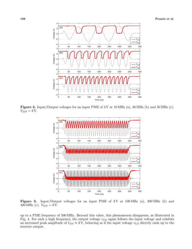
The effect of the PME is functionally observed on the measurement of the output voltage of the MOSinverter shown in the center part of Fig. 1. The curves in Fig. 2 are input/output voltage waveformsfor frequencies of 10 MHz, 30 MHz and 50 MHz with the same peak value of 3 V of the PME applied tothe gate terminal. These plots depict vDS voltages exhibiting a logic waveform in response to the PMEexcitation. In essence, the inverter follows the input frequency.
Figs. 3(a) and (b) show the alteration of the inverter response when the frequency is increasedto 100 MHz or 200 MHz. The output voltage vDS no longer looks like a logic waveform and the vDS
voltage swing decreases with frequency. At the frequency of 400 MHz (see Fig. 3(c)) this voltage swingis so reduced that the inverter output is a sine signal between −0.7 V and +0.7 V. In fact, as the carrierfrequency increases, the inverter response tends to reproduce the opposite of the pulse envelope witha small amount of the RF signal superimposed, the latter being so small at 400 MHz that the outputsignal is always below the commutation threshold of a classic logic gate. As a main result, the inputof any logic block following the inverter will be totally inhibited and pinned on the lower logic level.We get a blocking of the output state, while we were expecting a tracking of the control voltage. Thiseffect will be hereafter referred to as the “blocked state” of the inverter. This blocked state occurs
188 Pouant et al.
0 50 100 150 200 250 300 350 400
Vol
tage
(V
)
-4
-2
0
2
4
VGS
VDS
0 50 100 150 200 250 300 350 400
Vol
tage
(V
)
-4
-2
0
2
4
VGS
VDS
Time (ns)0 50 100 150 200 250 300 350 400
Vol
tage
(V
)
-4
-2
0
2
4
VGS
VDS
(b)
(a)
(c)
Figure 2. Input/Output voltages for an input PME of 3V at 10 MHz (a), 30 MHz (b) and 50 MHz (c).VDD = 3 V.
0 50 100 150 200 250 300 350 400
Vol
tage
(V
)
-4
-2
0
2
4
VGS
VDS
0 50 100 150 200 250 300 350 400
Vol
tage
(V
)
-4
-2
0
2
4
VGS
VDS
Time (ns)0 50 100 150 200 250 300 350 400
Vol
tage
(V
)
-4
-2
0
2
4
VGS
VDS
(b)
(a)
(c)
Figure 3. Input/Output voltages for an input PME of 3 V at 100 MHz (a), 200 MHz (b) and400 MHz (c). VDD = 3 V.
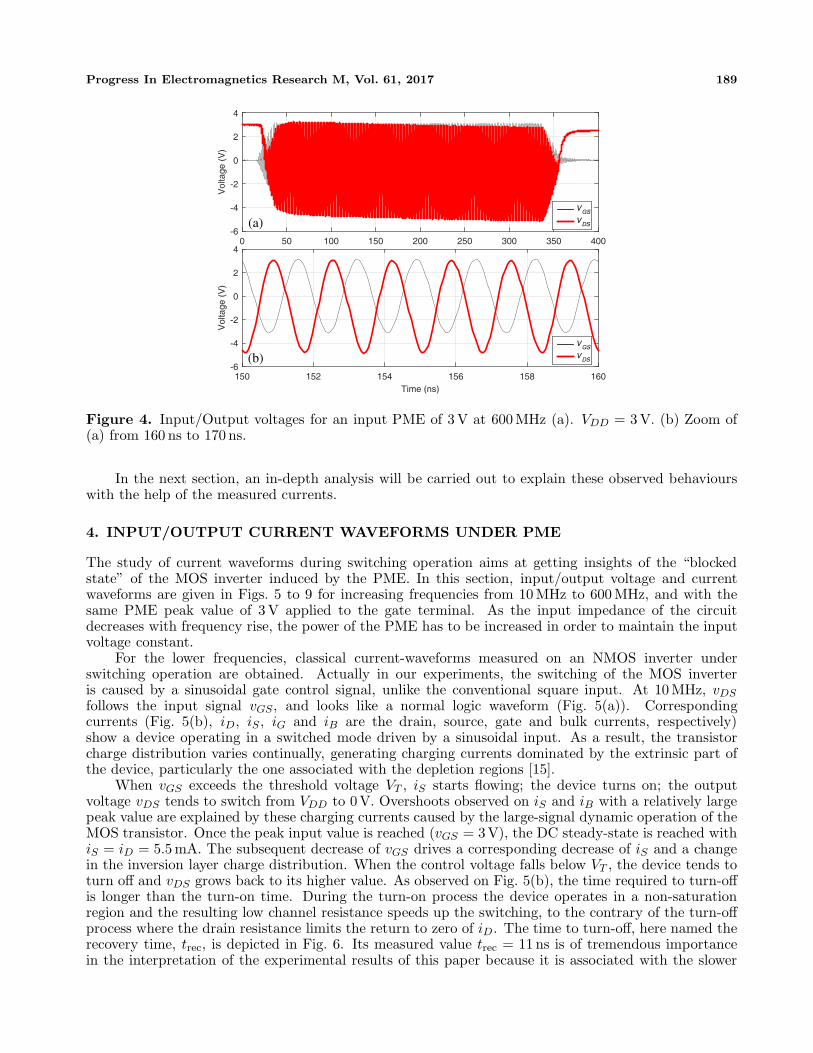
up to a PME frequency of 500 MHz. Beyond this value, this phenomenon disappears, as illustrated inFig. 4. For such a high frequency, the output voltage vDS again follows the input voltage and exhibitsan increased peak amplitude of vDS ≈ 3 V, behaving as if the input voltage vGS directly ends up to theinverter output.
Progress In Electromagnetics Research M, Vol. 61, 2017 189
0 50 100 150 200 250 300 350 400
Vol
tage
(V
)-6
-4
-2
0
2
4
VGS
VDS
Time (ns)150 152 154 156 158 160
Vol
tage
(V
)
-6
-4
-2
0
2
4
VGS
VDS
(a)
(b)
Figure 4. Input/Output voltages for an input PME of 3 V at 600 MHz (a). VDD = 3 V. (b) Zoom of(a) from 160 ns to 170 ns.
In the next section, an in-depth analysis will be carried out to explain these observed behaviourswith the help of the measured currents.
4. INPUT/OUTPUT CURRENT WAVEFORMS UNDER PME
The study of current waveforms during switching operation aims at getting insights of the “blockedstate” of the MOS inverter induced by the PME. In this section, input/output voltage and currentwaveforms are given in Figs. 5 to 9 for increasing frequencies from 10 MHz to 600 MHz, and with thesame PME peak value of 3 V applied to the gate terminal. As the input impedance of the circuitdecreases with frequency rise, the power of the PME has to be increased in order to maintain the inputvoltage constant.
For the lower frequencies, classical current-waveforms measured on an NMOS inverter underswitching operation are obtained. Actually in our experiments, the switching of the MOS inverteris caused by a sinusoidal gate control signal, unlike the conventional square input. At 10 MHz, vDS
follows the input signal vGS, and looks like a normal logic waveform (Fig. 5(a)). Correspondingcurrents (Fig. 5(b), iD, iS , iG and iB are the drain, source, gate and bulk currents, respectively)show a device operating in a switched mode driven by a sinusoidal input. As a result, the transistorcharge distribution varies continually, generating charging currents dominated by the extrinsic part ofthe device, particularly the one associated with the depletion regions [15].
When vGS exceeds the threshold voltage VT , iS starts flowing; the device turns on; the outputvoltage vDS tends to switch from VDD to 0V. Overshoots observed on iS and iB with a relatively largepeak value are explained by these charging currents caused by the large-signal dynamic operation of theMOS transistor. Once the peak input value is reached (vGS = 3V), the DC steady-state is reached withiS = iD = 5.5 mA. The subsequent decrease of vGS drives a corresponding decrease of iS and a changein the inversion layer charge distribution. When the control voltage falls below VT , the device tends toturn off and vDS grows back to its higher value. As observed on Fig. 5(b), the time required to turn-offis longer than the turn-on time. During the turn-on process the device operates in a non-saturationregion and the resulting low channel resistance speeds up the switching, to the contrary of the turn-offprocess where the drain resistance limits the return to zero of iD. The time to turn-off, here named therecovery time, trec, is depicted in Fig. 6. Its measured value trec = 11 ns is of tremendous importancein the interpretation of the experimental results of this paper because it is associated with the slower

190 Pouant et al.
150 160 170 180 190 200 210 220 230 240 250
Vol
tage
(V
)-4
-3
-2
-1
0
1
2
3
4
VT
VGS
VDS
Time (ns)150 160 170 180 190 200 210 220 230 240 250
Cur
rent
(m
A)
-2
0
2
4
6
8iDiSiGiB
(a)
(b)
Figure 5. Zoom of Input/Output voltages and currents of a MOS inverter with a 10 MHz/3 V PMEapplied (VDD = 3 V). (a) Voltages. (b) Currents.
190 195 200 205 210 215 220
Vol
tage
(V
)
-4
-3
-2
-1
0
1
2
3
4
VT
trec
VGS
VDS
Time (ns)190 195 200 205 210 215 220
Cur
rent
(m
A)
-5
0
5
10
15iD iS iG iB
(a)
(b)
Figure 6. Zoom of Input/Output voltages and currents of a MOS inverter with a 50 MHz/3 V PMEapplied (VDD = 3 V). (a) Voltages. (b) Currents.
process.At 50 MHz (see Fig. 6), the qualitative behaviour of the switching process is similar to that observed
at lower frequency. All currents exhibit shapes similar to that obtained at 10 MHz. Once the peak inputvalue is reached, the drain current reaches its DC steady state value iD = 5.5 mA, with the same turn-ontime. Overshoots of source and substrate currents are more intense because of the larger dvGS/dt thatdrives higher charging currents. Let us note that the off-state of the transistor is barely reached.
Increasing further the PME frequencies lead to a non-logic waveform for vDS , close to a sawtooth,with a peak-to peak drain voltage that tends also to decrease. The input voltage period, T ≈ 10 ns,now smaller than trec, indeed limits the vDS increase rate and its previous maximum value VDD = 3 Vis no longer reached (see e.g., Fig. 7(a) at 100 MHz). At the same time the DC steady-state value

Progress In Electromagnetics Research M, Vol. 61, 2017 191
190 195 200 205 210 215 220
Vol
tage
(V
)-4
-3
-2
-1
0
1
2
3
4
VT
VGS
VDS
Time (ns)190 195 200 205 210 215 220
Cur
rent
(m
A)
-15
-10
-5
0
5
10
15
20
iDiS
iGiB
(a)
(b)
Figure 7. Zoom of Input/Output voltages and currents of a MOS inverter with a 100 MHz/3 V PMEapplied (VDD = 3 V). (a) Voltages. (b) Currents.
190 192 194 196 198 200
Vol
tage
(V
)
-4
-3
-2
-1
0
1
2
3
4
VT
VGS
VDS
Time (ns)190 192 194 196 198 200
Cur
rent
(m
A)
-60
-40
-20
0
20
40
60
iDiS
iGiB
(a)
(b)
Figure 8. Zoom of Input/Output voltages and currents of a MOS inverter with a 400 MHz/3 V PMEapplied (VDD = 3 V). (a) Voltages. (b) Currents.
iD = 5.5 mA is still reached, but during the turn-off process. Since the drain current never vanishes,the device is never off. The iD-waveform now differs from the half-wave rectified current observed atlow frequencies, where iD flows only when vGS ≥ VT . The consequence is an increase of iD, the meanvalue of iD, and according to the load-line of the inverter, a decrease of vDS , the mean value of vDS.
When switching to 400 MHz (Fig. 8), the effects previously pointed out are reinforced. The vDS-waveform is very close to a sine of 1V peak voltage superimposed to a DC component. Waveformsof Fig. 8(a) correspond to a “blocked state” of the inverter, lasting as long as the pulsed RF signal isapplied. The period of the driven voltage vGS is 2.5 ns, a value nearly four time shorter than trec. Asalready mentioned iD no more vanishes and consequently iD further increases while vDS decreases. Inthe same time, vDSp-p , the vDS swing, also tends to decrease with the PME frequency. To the contrary,

192 Pouant et al.
190 191 192 193 194 195 196V
olta
ge (
V)
-6
-4
-2
0
2
4
VT
VGS
VDS
Time (ns)190 191 192 193 194 195 196
Cur
rent
(m
A)
-200
-100
0
100
200
iDiS
iGiB
(a)
(b)
Figure 9. Zoom of Input/Output voltages and currents of a MOS inverter with a 600 MHz/3 V PMEapplied (VDD = 3 V). (a) Voltages. (b) Currents.
we observe a noticeable increase in the amplitude of source, gate and bulk currents. Moreover iD isdelayed with respect to the control voltage and its peak value of 7.5 mA is slightly higher than the DCsteady-state value of 5.5 mA. The frequency of the control signal is now so high that the device reactsmore to the time-variation of the input voltage than to its absolute value. At such high frequency, theimpedances associated with the strong extrinsic capacitances of the device become so small that theylead to a “blocked state” of the MOS inverter.
A further increase of frequency to 600 MHz together with a constant peak value of 3V appliedto the gate produces the waveforms given in Fig. 9. The inverter is no more in its “blocked state”and all currents are almost sinusoidal. Reasons are the too fast vGS changes with respect to the MOScharges that are unable to follow such a rapid variation. The major part of the current flows throughthe inverter using shortcuts brought by the parasitic and external elements. Above 600 MHz new pathsfor the electromagnetic interference are opened by these parasitics, which shunt any transistor action,namely the classical intrinsic non-linearities associated with the transport current.
5. NUMERICAL SIMULATION
SPICE-like simulations were performed with Keysight ADS software to bring additional information,particularly regarding extrinsic parasitics that are believed mandatory to understand the circuitdisruption. Note that our purpose here is not to reach a perfect fit between experimental and simulatedresults, but instead to confirm and identify the parasitics that drive the observed response of our inverter.
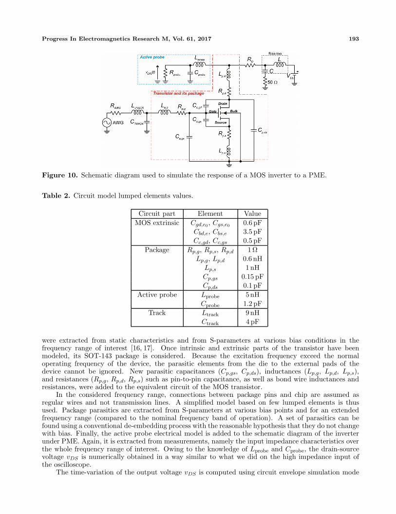
Lumped elements models are used for the transistor, package, tracks and active probe measuringvDS. They are all represented in Fig. 10 with values in Table 2, and will be discussed step by step.
The MOS inverter is simulated using the compact model Philips MOS Model 9. This choice is fullyappropriate to the present device. This model is simplified in that only few input parameters are requiredand should be determined from experiments. As for the intrinsic MOS, parameters values are obtainedfrom the measured DC characteristics and the gate-to-channel capacitance. All charge storage providedby the extrinsic part of the MOS are modeled via bias-dependent and layout-dependent capacitances.They account for the overlap of the gate over both source and drain extensions (Cgs,e0 and Cgd,e0), thebody-source and body-drain junctions (Cbs,e and Cbd,e), and for layout-dependent capacitances becauseof the large source and drain contacts (Cc,gs and Cc,gd). The only extrinsic resistance taken intoaccount is the gate resistance because of its importance for high speed and RF signals. Bias-dependentcapacitances and gate resistance are included in Philips MOS Model 9, and contact capacitances areadded outside this model (cf Fig. 10). Parameters describing the DC characteristics and storage effects
Progress In Electromagnetics Research M, Vol. 61, 2017 193
Figure 10. Schematic diagram used to simulate the response of a MOS inverter to a PME.
Table 2. Circuit model lumped elements values.
Circuit part Element ValueMOS extrinsic Cgd,e0, Cgs,e0 0.6 pF
Cbd,e, Cbs,e 3.5 pFCc,gd, Cc,gs 0.5 pF
Package Rp,g, Rp,s, Rp,d 1 ΩLp,g, Lp,d 0.6 nH
Lp,s 1 nHCp,gs 0.15 pFCp,ds 0.1 pF
Active probe Lprobe 5 nHCprobe 1.2 pF
Track Ltrack 9 nHCtrack 4 pF
were extracted from static characteristics and from S-parameters at various bias conditions in thefrequency range of interest [16, 17]. Once intrinsic and extrinsic parts of the transistor have beenmodeled, its SOT-143 package is considered. Because the excitation frequency exceed the normaloperating frequency of the device, the parasitic elements from the die to the external pads of thedevice cannot be ignored. New parasitic capacitances (Cp,gs, Cp,ds), inductances (Lp,g, Lp,d, Lp,s),and resistances (Rp,g, Rp,d, Rp,s) such as pin-to-pin capacitance, as well as bond wire inductances andresistances, were added to the equivalent circuit of the MOS transistor.
In the considered frequency range, connections between package pins and chip are assumed asregular wires and not transmission lines. A simplified model based on few lumped elements is thusused. Package parasitics are extracted from S-parameters at various bias points and for an extendedfrequency range (compared to the nominal frequency band of operation). A set of parasitics can befound using a conventional de-embedding process with the reasonable hypothesis that they do not changewith bias. Finally, the active probe electrical model is added to the schematic diagram of the inverterunder PME. Again, it is extracted from measurements, namely the input impedance characteristics overthe whole frequency range of interest. Owing to the knowledge of Lprobe and Cprobe, the drain-sourcevoltage vDS is numerically obtained in a way similar to what we did on the high impedance input ofthe oscilloscope.
The time-variation of the output voltage vDS is computed using circuit envelope simulation mode

194 Pouant et al.
101 102 103
Ave
rage
out
put v
olta
ge (
V)
-4
-3
-2
-1
0
1
2
3
4 Simulation
Measure
Frequency (MHz)101 102 103
Pea
k-to
-pea
k ou
tput
vol
tage
(V
)
0
2
4
6
8
10
12 Simulation
Measure
(a)
(b)
Figure 11. Comparison between measured (stars) and calculated (circles) outputs of the inverter as afunction of the PME frequency, (a) average output voltage, (b) peak-to-peak output voltage.
of ADS. This technique consists in an harmonic balance analysis with time-varying envelop thatparticularly suits the PME modulated excitation signal used here. Note that a classical transientsimulation-mode could also be used. The steady-state output of the nonlinear circuit is thus computedover a specified duration chosen in accordance with the repetition time of the PME. To compare withexperiments we summarized the experimental time traces of Figs. 2–4 during the application of thePME with vDSp-p and vDS. These two values were also calculated with the numerical model and theresults are both plotted for comparison in Fig. 11 as a function of f , the carrier frequency of the PME.
Both the measured and computed results show a regular decrease of vDS with f . The evolutionof vDSp-p is a little bit more complicated and exhibits a sudden regrowth above 400 MHz accordingto the resonance brought by parasitics, the latter being estimated ≈ 700 MHz from values of Table 2.The internal gate voltage is thus far much higher than the one externally fed to the device. Again,both the experimental and computed curves compare favorably. The “blocked state” of the inverteris thus highlighted for frequencies between approximately 100 MHz and 400 MHz. In fact, thecorrespondence between calculations and experiments was only possible when accounting for all theparasitics surrounding the ADS Philips MOS Model 9. It confirms the tremendous role played by allMOS extrinsic elements but also by the parasitics brought by the package and the PCB tracks, that acttogether in the occurrence of the circuit disruption observed experimentally.
6. CONCLUSION
In this paper, we have experimentally studied the electromagnetic susceptibility of the MOS transistorto PME. The methodology and equipment setup for direct injection experiments and acquisitionof all transistor instantaneous currents/voltages developed here have helped to get insights of theunderstanding of PME effects on MOS technology at the device level.
Experimental results have highlighted the dramatic effect of electromagnetic interferences that maylead to a “blocked state” of a MOS inverter. In this particular state, the output is maintained in aconstant low state as long as the RF pulse is applied, and the transistor no more follows the controlvoltage vGS . It was shown to occur if the excitation frequency is set within a bandwidth just beyondthe maximum switching frequency of the inverter.
The analysis of current waveforms during this “blocked state” has led to the conclusion that theMOS transistor’s extrinsic elements and the PCB parasitics play a very important role in the occurrenceof this effect. Numerical simulations have confirmed this point, as the phenomenon only appeared if

Progress In Electromagnetics Research M, Vol. 61, 2017 195
these elements were taken into account.This “blocked state” could potentially generate upset events in larger electronic systems and will
certainly also appear on more recent MOS technologies, but probably at higher frequencies becauseintrinsic and extrinsic capacitances are indeed reduced when shortening the gate length. The knowledgeof the involved physical mechanisms is the basis to accurately understand the EM susceptibility. Fromthe defender viewpoint, this study may help to predict how PME can upset circuits and thereby help indesigning more robust electronic systems. From the attacker side, it can be useful to upset the targetedsystem more efficiently.
REFERENCES
1. Ni, G., B. Gao, and J. Lu, “Research on high power microwave weapons,” IEEE Asia-PacificMicrowave Conference, 10–14, 2005.
2. Backstrom, M. and K. Lovstrand, “Susceptibility of electronic systems to high-power microwaves:summary of test experience,” IEEE Trans. Electromagn. Compat., Vol. 46, No. 3, 396–403, 2004.
3. Hwang, S.-M., J.-I. Hong, and C.-S. Huh, “Characterization of the susceptibility of integratedcircuits with induction caused by high power microwaves,” Progress In Electromagnetics Research,Vol. 81, 61–72, 2008.
4. Wang, H., J. Li, H. Li, K. Xiao, and H. Chen, “Experimental study and spice simulation of CMOSinverters latch-up effects due to high power microwave interference,” Progress In ElectromagneticsResearch, Vol. 87, 313–330, 2008.
5. Tsai, H.-C., “Reliable study of digital IC circuits with margin voltage among variable DC powersupply, electromagnetic interference and conducting wire antenna,” Microelectron. Reliab., Vol. 43,No. 12, 2001–2009, 2003.
6. Forcier, M. and R. Richardson, “Microwave-rectification RFI response in field-effect transistors,”IEEE Trans. Electromagn. Compat., Vol. 21, No. 4, 312–315, 1979.
7. Richardson, R., “Quiescent operating point shift in bipolar transistors with AC excitation,” IEEEJ. of Solid-State Cir., Vol. 14, No. 6, 1087–1094, 1979.
8. Richardson, R., “Modeling of low-level rectification RFI in bipolar circuitry,” IEEE Trans.Electromagn. Compat., Vol. 21, No. 4, 307–311, 1979.
9. Richardson, R., V. Puglielli, and R. A. Amadori, “Microwave interference effect in bipolartransistors,” IEEE Trans. Electromagn. Compat., Vol. 17, No. 4, 216–219, 1975.
10. Jovic, O., C. Maier, and A. Baric, “High-voltage PMOS transistor model for prediction ofsusceptibility to conducted interference,” IEEE Trans. Electromagn. Compat., Vol. 53, No. 1, 53–62,2011.
11. Pouant, C., J. Raoult, and P. Hoffmann, “Large domain validity of MOSFET microwave-rectification response,” IEEE 10th International Electromagnetic Compatibility of IntegratedCircuits, 232–237, 2015.
12. Holloway, M., Z. Dilli, N. Seekhao, and J. Rodgers, “Study of basic effects of HPM pulses in digitalCMOS integrated circuit inputs,” IEEE Trans. Electromagn. Compat., Vol. 54, No. 5, 1017–1027,2012.
13. Op’t Land, S. T., M. Ramdani, R. Perdriau, M. Leone, and M. Drissi, “Simple, Taylor-based worst-case model for field-to-line coupling,” Progress In Electromagnetics Research, Vol. 140, 297–311,2013.
14. Sicard, E. and J. Dienot, “Issues in electromagnetic compatibility of integrated circuits: emissionand susceptibility,” Microelectron. Reliab., Vol. 45, No. 9, 1277–1284, 2005.
15. Tsividis, Y. and C. McAndrew, Operation and Modeling of the MOS Transistor, Oxford Univ.Press, 2011.
16. Cheng, Y., M. Deen, and C.-H. Chen, “MOSFET modeling for RF IC design,” IEEE Trans. Elect.Dev., Vol. 52, No. 7, 1286–1303, 2005.
17. Kwon, I., M. Je, K. Lee, and H. Shin, “A simple and analytical parameter-extraction method of amicrowave MOSFET,” IEEE Trans. Microw. Theory Tech., Vol. 50, No. 6, 1503–1509, 2002.