copyright © 1982, by the author(s). all rights reserved
TRANSCRIPT

Copyright © 1982, by the author(s). All rights reserved.
Permission to make digital or hard copies of all or part of this work for personal or
classroom use is granted without fee provided that copies are not made or distributed for profit or commercial advantage and that copies bear this notice and the full citation
on the first page. To copy otherwise, to republish, to post on servers or to redistribute to lists, requires prior specific permission.

RELAX: A NEW CIRCUIT SIMULATOR FOR LARGE
SCALE MOS INTEGRATED CIRCUITS
by
E. Lelarasmee and A. Sangiovanni-Vincentelli
Memorandum No. UCB/ERL M82/6
5 February 1982
RELAX: A NEW CIRCUIT SIMULATOR FOR LARGE
SCALE MOS INTEGRATED CIRCUITS
by
E. Lelarasmee and A. Sangiovanni-Vincentelli
Memorandum No. UCB/ERL M82/6
5 February 1982
ELECTRONICS RESEARCH LABORATORY
College of EngineeringUniversity of California, Berkeley
94720

RELAX : A new circuit simulator for large
SCALE MOS INTEGRATED CIRCUITS.
E. LELARASMEE AND A, SANGIOVANNI-VINCENTELLI
ABSTRACT
Algorithms and techniques used in RELAX are described. RELAX
is a time domain simulator based on a new analysis method called
Waveform Relaxation Method (1) which exploits decomposition
techniques. Preliminary comparisons between RELAX and the
standard circuit simulator SPICE2 have shown that RELAX is a fast
and reliable circuit simulator.
Department of EECS, University of California,
Berkeley, CA. 94720 (on leave at Harris Semiconductor
Products Division, Melbourne, Florida, 32901).
This -research was supported in parts by grants from
Harris Corporation and IBM Corporation, and by the
Defense Advanced Research Projects Agency (DOD) Contract
N00039-K-0251.

I. INTRODUCTION
In the VLSI era, the demand for time domain circuit simulation
of larger and larger circuits is continuously growing in the
industrial designers community. Consequently, the use of standard
general purpose circuit simulators such as SPICE (2) and ASTAP (3)
is becoming too expensive. Alternative methods have been proposed
for the electrical analysis of large scale circuits to reduce the
CPU time and storage requirement. A survey of these methods is
given in (4). These methods rely on the decomposition of the circuit
equations at various levels (i.e. linear, nonlinear and differential).
Among them, timing simulation first introduced'in MOTIS (£1 is perhaps
the most well known method. The solution method upon which timing
simulators are based applies decomposition to the nonlinear equations
derived from the discretization of the differential equations describing
the circuit to be analysed. The implementation of decomposition
together with an event scheduling scheme in mixed-mode simulators such
as SPLICE C61 and DIANA Qi)_ leads to electrical simulators which
are considerably faster than standard circuit simulators. However,
recent studies (71 nave shown that timing simulation algorithms tend -
to handle poorly circuits containing tight couplings between subcircuits
(e.g. floating capacitive couplings and pass transistor couplings) and
have stability problems. Hence these algorithms are suitable to a
restricted class of circuits: MOS circuits with quasi-unidirectional
device models.
This paper describes a new MOS circuit simulator RELAX.
RELAX uses a new analysis method called Waveform Relaxation Method
which is fully described in (l) , This method is based on the
decomposition of the differential equations describing the
circuit to be analysed. Theoretical studies (1) have shown that,
under very mild conditions which are usually satisfied in practice,
the method has guaranteed convergence when applied to MOS circuits.
Preliminary tests indicate that RELAX is at least one order of
magnitude faster than the standard circuit simulator SPICE2 with
the same accuracy.
This paper is organized as follows. Section II gives a brief
overview of the Waveform Relaxation Method and its circuit
interpretation. Section III describes the basic techniques used
in RELAX to implement the method. In particular, the scheduling
algorithm and the techniques to speed up the analysis are described
in detail. Section IV gives the organization of RELAX and Section V
shows some experimental tests and comparisons with the standard
circuit simulator SPICE2.
9-

II. Outline of the Waveform Relaxation Method
In this section we give the basic concepts of the Waveform
Relaxation Method (WRM) which is the heart of the algorithm used in
RELAX. WRM is an iterative method based on a relaxation scheme which
applies decomposition directly to the system of differential equations
describing the dynamical behaviour of the circuit to be analysed. The
method can be easily explained by its application to a circuit described
by the following differential equations.
•
*(x(t), xCt), u(t) ) « 0 ; x(o) o Xq (2.1)
.rwhere u(.t) 6 R is the vector of input voltages and their time
n • «
derivatives, x(t) € R is the vector of unknown node voltages, x(t) e R
is the vector of the time derivative of x, xQ € Rn is the given initialvalue of x and f: Rnx Rnx Rr * Rn is a continuous map.
WRM procedure to analyse (2.1) from t»o to t«T .
Comments: the superscript k denotes the iteration count, the subscript i
denotes the component index of a vector and £ is a small
positive number.
Step 1 : (.Initialization)
Set k=o and make an initial guess of the waveform° r 1 Ox(t) ; t€ [o,TJ such that x(o) « xQ .
3

Step 2: .(Iteration)
Repeat
k - k+1
For i» 1, 2, ..., n
Begin
Solve for x* (t) ;t € [o,t] from
•k *k »k-l «k-l^i ,..., X. , X. ^- ,..., X
k k k-1 kX* ,..., X . , X .̂ -m ,..., X
with x (o) • x^o
• u) « o (2.2)
End
k k-1
Until max max |x.(t) - x. (t) |< £ .
l<i<n tero,T](i.e. the iteration converges).
Note that equation (2.2) has only one unknown variable x. . The variables
k-1 k-1
x.+, ,..., x are known from the previous iteration and the variables
k kx1 ,..., x._, have already been computed.
As an example, consider the MOS circuit shown in Fig. 2.1. For the
sake of simplicity we assume that all capacitors are linear. Hence the
dynamical behaviour of the circuit can be described as follows:
• • *
t-cl+c2+c3) vl " il^vl) + i2^vl'u) + i3Cvl'u2'V2) " C1U1 " C3U2 = ° (2-3a)
Y
CVC5+C6^2 -C6V3 "WW ~c4»2 *Q f2'3h)
(c6+c7)v3 - c6v2 - i4Cv3l + i5Cv3.v2) - Q C2.3c)
Applying the WRM procedure to (2.31, the k.-th. iteratton corresponds
to solving the following equations:
(cl+c2+c3^1 "1l(-^> +^O^.ui +l3CvJ.U3.vJ-1) -c1u1-c3ia- 0(2.4al
5

<VW *2 "^T1 " i3('Vl' U2' V2> " c4*2 =° (2*4b)
*k #k(c6+c7) v3 - c6v2 _i4(v|) + i5(v£, v*) =o (2.4c)
The circuit interpretation of equation (2.4) is shown in figure 2.2.
If we consider that the original circuit in figure 2.1 consists of
3 subcircuits s,, s2 and s3, then the decomposed subcircuits S,, S« and So
shown in Figure 2.2 are actually s,, s2, and s« together with additional
components to approximate the loading effects due to the rest of the
circuit. Hence we can describe the WRM procedure for analyzing the
circuit in Fig. 3.1 in circuit terms as follows:
Step 1: Set k=o and make an initial guess of v°(t), v°(t); t€[o,T].
Step 2: Repeat
k * k+1
]rAnalyses, fcr its output waveform v,(.) by approximating
the loading effect due to s2.
k kAnalyse s2 for its output waveform v2(.) by using v1(.) as
its input and approximating the loading effect due to s3-
k kAnalyse s« for its output waveform v«(.) by using v2(.)
as its input. "-

Until the difference between {(v*(t), v2(t), v£(t); te [o,T]}
andCv*""1^), v2-1(t), Vg"1^); t€ [0,T]} is sufficiently small.
From the above procedure and example we see that each component of
the decomposition is a dynamical subcircuit which is processed for the
entire time interval [o,T] in a fixed order. When each subcircuit is
being processed, the interactions (or couplings or loadings) from the
rest of the circuit are approximated by using the information obtained frorr
the most recent iteration. The iteration is carried out until satisfactory
convergence of all waveforms is detected. It can be shown (l) that for th
MOS circuit in fig. 2.1 the sequence of waveforms generated by the WRM
procedure will always converge to the correct waveform independent of the
initial guess provided that c2, cg and c- are non zero. This result can
be generalized to any MOS circuit in which th.ere is a grounded Clinear or
nonlinear) capacitor to every output node of every subcircuit. This
condition for convergence is very mild for any practical MOS circuit.
Hence WRM can handle any MOS circuit containing tight couplings between
subcircuits such as logic feedbacks, pass transistor couplings and
floating capacitive couplings without losing its convergence property.
The rate of convergence is linear, a typical result for relaxation methods.
7

d«—t—ir l
•tsr
!i
♦ wt
« v: &«*
%T
-4.
Fig. 2.1 An MOS dynamic shift register.
•V"
4.
it XI
i!r»o
'Is
Fig. 2.2 The resulting decomposition of the circuit in Fig. 2.1at the k-th iteration of the WRM procedure.
8-

III. Basic Algorithms in RELAX
RELAX implements a modified version of the WRM procedure described
in the previous section. These modifications are done to improve the
speed of convergence of the algorithm and exploit the structure of the
class of circuits to be analysed, i.e., MOS digital circuits. These
modifications are described as follows.
3.1) Rather than having strictly one unknown per each component of the
decomposition as stated in the previous section, RELAX allows each
decomposed subcircuit - to have more than one unknown. In fact RELAX
decomposes the circuit to be analysed into subcircuits each of which
corresponds to a physical subcircuit specified by the user such as NOR,
NAND, etc.
3.2) Each decomposed subcircuit is processed by using standard circuit
analysis techniques. Backward Euler integration method with variable
timesteps is used to discretize the differential equations associated with
the subcircuit and the Newton-Raphson method is used to solve the nonlinear
algebraic equations resulting from the discretization. Since the number of
unknowns associated with a subcircuit is usually small, the linear equation
solver used by the Newton-Raphson method is implemented by using standard .
full matrix techniques rather than using sparse matrix techniques. Note
that in RELAX each subcircuit is analysed independently from t=o to t=T
using its own timestep sequence controlled by the integration method, while
<?

in a standard circuit simulator the entire circuit is analysed from
t=o to t*T using only one common timestep sequence. In RELAX, the timestep
sequence of one subcircuit is usually different from the others but
contains, in general, a smaller number of timesteps than that used in a
standard circuit simulator for analysing, the same circuit.
3.3) The order according to which each subcircuit is processed is
determined in RELAX prior to starting the iteration by a subroutine called
"scheduler". Although it has been shown (1) that scheduling is not
necessary to guarantee convergence of the iteration, it does have an impact
on the speed of convergence. Assume now that the circuit consists of
unidirectional subcircuits with no feedback path. If the subcircuits are
processed according to the flow of signals in the circuit, the algorithm
used in RELAX will converge in just two iterations (actually the second
iteration is needed only to verify that convergence has been obtained).
For MOS digital circuits which contain almost unidirectional subcircuits,
it is intuitive that convergence of the WRM procedure will be achieved more
rapidly if the subcircuits are processed according to the flow of signals
in the circuit. The scheduler traces the flow of signals through the
circuit and orders the processing of subcircuits accordingly. To be able
to trace the flow of signals, the scheduler requires the user to specify the
flow of signals through each subcircuit by partitioning the terminals of the
subcircuit into input and output terminals. In general, a designer can
easily specify what the flow of the signals is intended to be even in a
subcircuit which is not unidirectional such as a transmission gate or a
subcircuit containing floating capacitors between its input and output
terminals. Note that the analysis algorithm in RELAX will indeed take into

account the bidirectional effects .corr«ctly. To describe the algorithm
used by the scheduler, we need the following definition.
Definition 3.1 A subcircuit s2 is said to be a fanout of a subcircuit
s1 if an input terminal of s2 is connected to an output terminal of s^
i.e., an output of s^ is fed as an input to s2.
Before staring the scheduling algorithm, we point out tfait all
the input signals to the circuit are considered by the scheduler to be
contained in a special subcircuit called "source" subcircuit which is
essentially a subcircuit with only output terminals.
Scheduling algorithm:
Comment: X is an ordered set of subcircuits. At the compleiton
of the algorithm, x contains all the subcircuits and the
order in which each subcircuit is placed in x is the order
in which it is processed by RELAX.
Start: Set X « {source circuit} and Y »{fanouts of the source subcircuit }
Loop : Set Z • # i.e. clear the temporary set Z.
For each subcircuit s in Y
Begin
If (all inputs of s come from the outputs of subcircuitsin X) then
Begin
Delete s from Y and add it to £.Include in Z the fanouts of s which are not already inX,Y or Z
End
End ((

If (Z is not empty) then include Z in Y and go to Loop.
Else if (Y is empty) then stop
Else Begin comment: there is a feedback loop.
Select a subcircuit s from Y.
Delete s from Y and add it to X.
Include in Y the fanouts of s which are not already
in X or Y.
Go to Loop.
End.
For example, the set X produced by the scheduler applied to
the circuit of fig. 3.1 is { source, s^, S5, S4, s2, S3} and the
set X produced by the scheduler applied to the circuit of fig. 3.2
is {source, s2, S3, s^} .
3.4) The first iteration in RELAX is carried out by assuming that
there is no loading effect due to fanouts. The "standard" WRM
procedure actually begins at the second iteration in RELAX. Hence,
strictly speaking, the first iteration in RELAX is used to generate
a good initial guess for the actual WRM procedure.
aP-

In addition to the above modifications, RELAX incorporates
two important techniques to speed up the process of analysing a
subcircuit. The key idea is to bypass the analysis of a subcircuit
for certain time intervals without losing accuracy by exploiting
the information obtained from previous timepoints and/or from
previous iterations. Similar techniques have been used in other
simulators. For example, SPICE uses a bypass technique in its
Newton Raphson iteration. When a subvector of the vector of
unknowns does not change its value significantly in the previous two
Newton iterations, the part of the Jacobian matrix associated with
the subvector is not recomputed. SPLICE, on the other hand, uses an
event scheduling technique by which a subcircui-t is not scheduled
to be analyse at time t if it is found to be inactive.
The two techniques used in RELAX are discussed by showing its
application to the analysis of the subcircuit s^ of the circuit
shown in fig. 3.3, a schematic diagram of the circuit in fig. 2.1.
As in section 2, we denote the output voltages of s^ and s2 at the
k-th iteration by V^ and V§ respectively.
a) The first technique is based on the latency of s^ and is similar
to the technique described in (8) . According to 3.4, si is analysed
in the first iteration with no loading effect from s2. After it has
t?
been analysed for a few timepoints, its output voltage v^ is found
to be (almost) constant with time, i.e., ^(0.01) »0 (see fig. 3.3b).
Since the input of s^, i.e. u^, is also constant during the interval
[o.Ol, 1.9] ,v^ will also remain constant throughout the interval[o.Ol, 1.9J. The subcircuit s^ is then said to be latent in the
first iteration during the interval [o.Ol, 1.9] and its analysis
during this interval is bypassed. From fig. 3.3b, s^ is latent again
in the interval [2.15, 3J. Note that, according to 3.4, the check
for latency of s^ after the first iteration will include u2 and v2 as
well as ux since they can effect the value of vx (see fig. 2.2). For
most digital circuits, the latency intervals of a subcircuit usually
cover a large portion of the entire simulation time interval [0, t]
and hence the implementation of this technique can provide a considerable
saving of computing time as shown in Table 3.1.
b) The second technique is a unique feature of RELAX. It is based on
partial convergence of a waveform during the previous two iterations.
We introduce it by using the example of fig. 3.3 . After the first two
iterations, we observe that the values of vl and v? during, the
interval [l.7, 3.0J do not differ significantly (see fig. 3.3b, 3.3c
and 3.3©), i.e., the sequence of waveforms of v^ seems to converge in
this interval after two iterations. In the third iteration, shown in
fig. 3.3d, sx is analysed from t*0 to t*1.8 and v^(1.8) is found to bealmost the same as v^(1.8). Moreover, during the interval [l.8, 3J ,
<Y

2 **the values of u^, v2 and u2 which effect the value of vj3 (see fig.2.2)
also do not differ significantly from the values of u^, v^ and u2
which effect the value of v2 . Hence the value of v^ during the
interval [l.8, 3Jshould remain the same as v^ and the analysis of s^
during this interval in the third iteration will be bypassed. This
technique can provide a considerable saving of computing time as shown
in Table 3.1 since the intervals of convergence can cover a large
portion of the entire simulation time interval fo, t], especially in
the last few iterations. Note that the subcircuit need not be latent
during the intervals of convergence although overlapping of these
intervals with the latency intervals is possible.
/s

B 33> SUM
4>i3>-J CARRY
Fig. 3.1 A half adder.
TRIGGER
Fig. 3.2 A ring oscillator.
/&

Fig. 3.3 a) A dynamic shift register b), c) and d) Output
waveforms at the first, second and third WRM iteration
respectively.
e) The difference of the waveforms between the first and! .
second iteration.
rl 3
-_nw»
e o.s i.*
6.0
4,0
^fri-f^S2.0:
0.0^0.0 1.0
(b)
6.0
U4..|J"V*#^
= v. X I I "i
•J I i VU . «t*^ ii j?< i • i • 1 i i i i i t • . . •»[0 - 0 1.0 2.0
(d)
• • • '
1v>o • rn—,— iNo
(a)
6.9: i
4.0
:"\ j44JH+*|4-H--ftj
.0 =
Li,0 .0]•i i i fti i0.0
-1
I.dull
•H—hhi
1 I I ' t I ? I I I I 1 1 u1.0
(c)
» ' • ' I I
3.9

Table 3.1 Comparison of computer time used by RELAX
with and without the latency and partial waveform
convergence techniques.
iteration
number
CPU time (seconds)
case 1 case 2 case 3 case 4
1
2
3
4
5
0.363
0.824
0.821
0.828
0.832
0.255
0.704
0.705
0.704
0.695
0.360
0.814
0.242
0.151
0.097
0.258
0.695
0.238
0.104
0.016
Total 3.668 3.063 1.664 1.311
case 1 : without both latency and partial waveform convergence
techniques.
case 2 : with only latency technique.
case 3 : with only partial waveform convergence technique.
case 4 : with both latency and partial waveform convergence
techniques.
AT
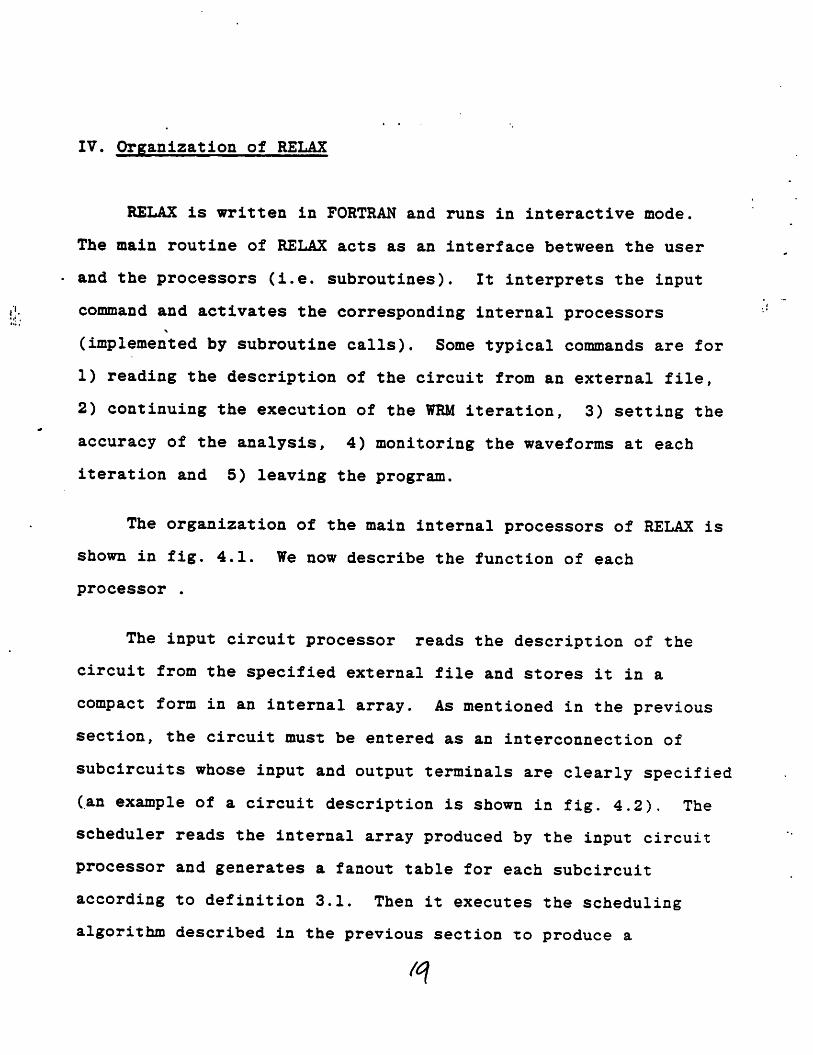
IV. Organization of RELAX
RELAX is written in FORTRAN and runs in interactive mode.
The main routine of RELAX acts as an interface between the user
and the processors (i.e. subroutines). It interprets the input
command and activates the corresponding internal processors
(implemented by subroutine calls). Some typical commands are for
1) reading the description of the circuit from an external file,
2) continuing the execution of the WRM iteration, 3) setting the
accuracy of the analysis, 4) monitoring the waveforms at each
iteration and 5) leaving the program.
The organization of the main internal processors of RELAX is
shown in fig. 4.1. We now describe the function of each
processor .
The input circuit processor reads the description of the
circuit from the specified external file and stores it in a
compact form in an internal array. As mentioned in the previous
section, the circuit must be entered as an interconnection of
subcircuits whose input and output terminals are clearly specified
(an example of a circuit description is shown in fig. 4.2). The
scheduler reads the internal array produced by the input circuit
processor and generates a fanout table for each subcircuit
according to definition 3.1. Then it executes the scheduling
algorithm described in the previous section to produce a

scheduling table that gives the order in which each subcircuit will be
processed in the WRM iteration. Both the input circuit processor
and the scheduler are actually preprocessing steps for the WRM
iteration since they are performed only once for the circuit to
be analysed.
The analysis of a subcircuit using the WRM iteration is
implemented in RELAX as a two-phase process: the setup phase
performed by the intermediate code generator and the analysis phase
performed by the subcircuit analyser. The intermediate code
generator reads the description of the subcircuit and its fanouts,
obtained by the input circuit processor and the scheduler, and
generates an intermediate code. This intermediate code is used by
the subcircuit analyser to analyse the subcircuit from t»o to
t=T, where T is the user-specified simulation time interval. The
subcircuit analyzer consists of several subroutines implementing the
integration method, the Newton-Raphson method, the linear equation
solver and the two techniques for speeding up the analysis discussed
in the previous section. The output and internal voltages of the
subcircuit at the sequence of timepoints used by the subcircuit
analyzer as well as the sequence of times are stored in an internal
waveform storage which stores the discretized waveforms associated
with all nodes in the circuit. To analyse a subcircuit at a timepoint,
say tj, the subcircuit analyzer has to know the values of its input
30
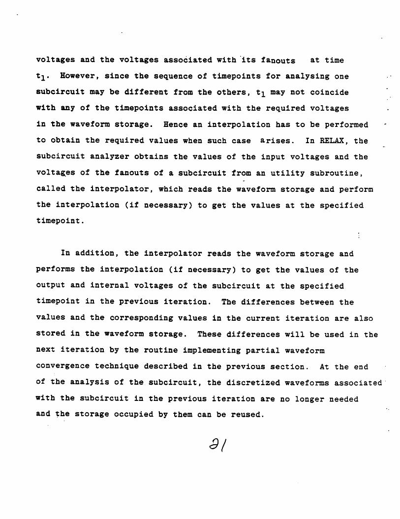
voltages and the voltages associated with its fanouts at time
t^. However, since the sequence of timepoints for analysing one
subcircuit may be different from the others, t]_ may not coincide
with any of the timepoints associated with the required voltages
in the waveform storage. Hence an interpolation has to be performed
to obtain the required values when such case arises. In RELAX, the
subcircuit analyzer obtains the values of the input voltages and the
voltages of the fanouts of a subcircuit from an utility subroutine,
called the interpolator, which reads the waveform storage and perform
the interpolation (if necessary) to get the values at the specified
timepoint.
In addition, the interpolator reads the waveform storage and
performs the interpolation (if necessary) to get the values of the
output and internal voltages of the subcircuit at the specified
timepoint in the previous iteration. The differences between the
values and the corresponding values in the current iteration are also
stored in the waveform storage. These differences will be used in the
next iteration by the routine implementing partial waveform
convergence technique described in the previous section. At the end
of the analysis of the subcircuit, the discretized waveforms associated
with the subcircuit in the previous iteration are no longer needed
and the storage occupied by them can be reused.
#1

At present, RELAX is still in an experimental stage, it
can handle MOS digital circuits containing NOR gates, NAND gates,
transmission gates, multiplexers (or bands of transmission gates
whose outputs are connected together), super buffers and
cross-coupled NOR gates (or flip-flops). It uses the Schichmann-
Hodges model (9) (or the level 1 MOS model used in SPICE2) for
the MOS device. All- the computations are performed in double
precis-ion and the results are also stored in double precision.
Although RELAX code is rather small, approximately 4000 FORTRAN
lines, it requires a considerably large amount of storage for the
waveforms, especially when large circuits are analysed. For an
MOS circuit containing 1000 nodes with 100 analysis timepoints per
node, the waveform storage is required to store approximately
3x1000x100 floating point numbers (corresponding to 2.4 megabytes
if each number is stored in 64 bits). Further enhancements of
RELAX are
1) Capability of handling user-defined subcircuits.
2) Provision of more accurate MOS models. The user, if desired,
can choose to use a simplified MOS model in the first few
iterations for a fast analysis and switch to a more accurate
model in the later iterations.
3) The implementation of storage buffering scheme. In this scheme,
the amount of primary storage allocation for the waveforms is
limited. When this storage is not enough to store all the
waveforms, a secondary storage such as a disk is used to supply
the additional storage needed. _^3-2-

Since the access time of the secondary storage is much longer than
that of the primary storage, the speed of the analysis of a
subcircuit will be greatly reduced if the interpolator has to
access the secondary storage directly in order to get the desired
values. The buffering scheme is designed to cope with this
situation and ensure that all the waveforms associated with the
analysis of a subcircuit already reside in the primary storage prior
to the beginning of the analysis of the subcircuit. This is achieved
by using the following algorithm.
Simplified storage buffering algorithm
Comment: s denotes the subcircuit currently being analysed and S
denotes the set of the waveforms required in the analysis
of s. For the sake of simplicity, we assume that the
storage of the waveforms associated with the output and
internal voltages of s in the previous iteration is re
used by the corresponding waveforms in the current
iteration. We also assume that S is in the primary storage
Loop: From the scheduling table, determine the next subcircuit
to be analysed.
Set S » {waveforms required in the analysis of the next
subcircuit } .
If (S is in the primary storage) then go to WAIT
Else Begin
£3
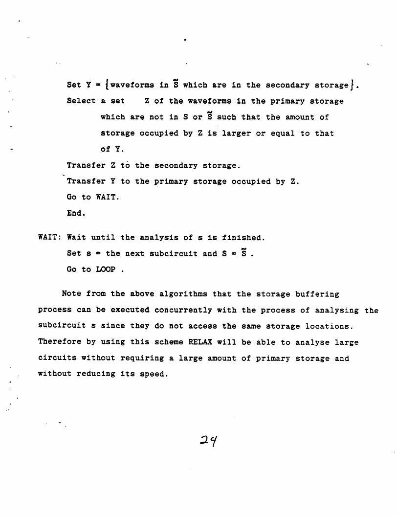
Set Y • {waveforms in S which are in the secondary storage] .
Select a set Z of the waveforms in the primary storage
which are not in S or S such that the amount of
storage occupied by Z is larger or equal to that
of Y.
Transfer Z to the secondary storage.
Transfer Y to the primary storage occupied by Z.
Go to WAIT.
End.
WAIT: Wait until the analysis of s is finished.
Set s * the next subcircuit and S • S .
Go to LOOP .
Note from the above algorithms that the storage buffering
process can be executed concurrently with the process of analysing the
subcircuit s since they do not access the same storage locations.
Therefore by using this scheme RELAX will be able to analyse large
circuits without requiring a large amount of primary storage and
without reducing its speed.
21

USER
MAIN ROUTINEOF RELAX |--*|(interpreter)
INPUT CIRCUIT
PROCESOR
SCHEDULER
INTERMEDIATECODE
GENERATOR
SUBCIRCUIT
ANALYZER
INTERPOLATOR
Fig. 4.1 Organization of RELAX
EXTERNAL FILE
(CIRCUIT DESCRIPTION ]I SUBCIRCUIT DESCRIPTIONS i
[ FANOUT TABLESI SCHEDULING TABLE
INTERMEDIATE CODE
WAVEFORM STORAGE

Comment: Description of the circuit shown in fig. 3.3 .
si inverter input » 1 output » 2
s2 inverter input « 3 output = 4
s3 transmission-gate input =5,2 output = 3
Comment: Description of the models of MOS transistors.
Model ENHANCE NMOS {MOS parameters such as threshold
voltages, transconductance, etc. }
Model DEPLETION NMOS {MOS parameters) .
Comment: The connectivity of each MOS device is described as
: MOS-name drain-node gate-node source-node body-node &
: MOS-model-name width length .
Comment: Description of transmission gate.
subcircuit transmission-gate input * source, gate output c drain
M0S1 drain gate source GROUND ENHANCE .vidth = lu length = lu
ends
Comment: Description of an inverter
subcircuit inverter input * A output = A
MOSload VDD A A GROUND DEPLETION width «= lu length = ly
MOSdriver A A GROUND GROUND ENHANCE width • 4u length = lu.
ends
fig. 4.2 Example of an input circuit description for
RELAX.
2Q>

V. RELAX: experimental results and a comparison with SPICE.
Several MOS digital circuits have been analysed by RELAX
and the results have been compared with those obtained by the
standard circuit simulator SPICE (version 2.D). In these tests,
the two simulators use the same MOS model, i.e. the Schichman-
Hodges model (or SPICE2 MOS model level=l), so that the
accuracy of RELAX can also be verified by using SPICE2 outputs
as references. The schematic diagrams of the MOS circuits being
tested and their output waveforms obtained by RELAX and SPICE2
are shown in Fig. 5.1 through Fig. 5.5 . For RELAX output
waveforms, each rectangular mark denotes the computed value at
every other two internal timepoints to illustrate the effect of
the implemented latency technique. The two simulators run on a
HARRIS computer model 550. A comparison of the CPU time spent by
each simulator is given in Table 5.1 . The tabulated CPU time for
SPICE is the total CPU-seconds spent by its transient analysis
routine. The tabulated CPU time for RELAX is the total CPU-seconds
spent by the intermediate code generator, the subcircuit analyzer
and the interpolator (see Fig. 4.1) . It is clear from the figures
and the table that RELAX can analyse MOS digital circuits at least
one order of magnitude faster than SPICE2 while achieving the same
accuracy. Preliminary comparisons (1) with the timing simulation
routine of SPLICE (6) also indicate that the speed of RELAX is at
the same order as the speed of a timing simulator.
5?

Fig. 5.1 Schematic diagram of a dynamic shift resistor and
the output waveforms obtained by RELAX and SPICE2
3ATA.2N r CLOCK
v; JL v.*ATA.IN t>
1"&ATA.OUT
CLOCK
m0 «*f »•*
* £ LAX
i i i i
0.0 3.0 9.0 ? 0
6.0 6.0
SPICE
4.0:
2.0P
©ATA. OUT
S .OP t 'I . ! I t I t JJ^J^J^ijJJJJJ^J^J 0.0L3.0 0.0 1.0 2.03.0 1.0 2.0 - . -j
P5-
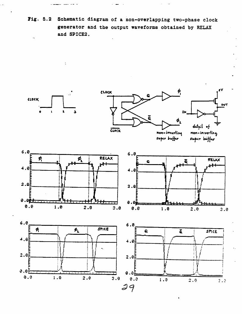
Fig. 5.2 Schematic diagram of a non-overlapping two-phase clock
generator and the output waveforms obtained by RELAX
and SPICE2.
clock
6.0
CLOCK
CLOCK
_ 6.1
cUiail ,f rnon- iwvAtti *d non• in vcrttn a.
OUT
4.0
I . .5 J RELAX
JL4.0
2.0:2.0
%0.0
g'S<" TT-JQlM. ...llfW 0 .©1=0 0.0
•gf*-fr-HH-»-
1 .
3D HJrWr2.0 3.9
6.06 .0
4.0
2.0£
0.0g—r-r
3.0

Fig. 5.3 Schematic diagram of a stack controller (from (10)page 73) and the output waveforms obtained by RELAXand SPICE2.
O 1 3
Phase I
o
rt 3
0? 10 I
6.0
J+4.0
: TRR$-4 8-**-++
TKasc 1» 9
TK**< I m
OP _*
ftELAX
T
6.0
e+
4.0
2.0
TRR
$HL
TRL
$HS
RELAX
SHR
e.eifciz 111i nfl-? j i :
i i t r i. » » i i • i1 ' ' ' ' * • •
0.0t± I t I I I > I I i i i i i . i i fi- \ j * \ 1 *r
0.0
6.0
4.0 TRR
Pc
0.0
1 .i
J.! > I
TTh \
1 .0
.0
2.0
3.0 0.0 1 .0 2.0 3.0
6.0
SPICE SPICE
Vx 4.0P ?5.T; / >
i I
2.0
2.0 0.O : .8
SO

Fig. 5.4 Schematic diagram of a dynamic shift-up register array
and the output waveforms obtained by RELAX and SPICE2.
CLOCK
SHlfT,
O I
6.0
4.0Qt
2.0
CLOCK
91
4—hHRELAX
r^T**id911 33
5l
/ K«4
CIRCUIT Of
c~
6.0
J+
4.0
2.0:
SHIFT-UP
*L >n
*,n.
T^T^^Rc~-
Ql
4?HQ\
«!^ *S>-*
j RELAX*-! HH
Ql
H0.
0.0*Tlt • ITflir i f i i i t 5 f
119-9 » 8'iti » i
1 .i 2.0
0.0f.3, , ,77773.0 0.0 1. 2.0 3.0
6.0 6.0
SPKS
&i \x Si
\i
•''''•
1 .0 . • y
?/
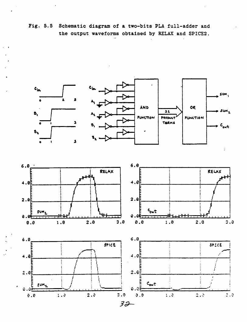
Fig. 5.5 Schematic diagram of a two-bits PLA full-adder and
the output waveforms obtained by RELAX and SPICE2.
0
r1 3
"JO I J
8»JO I
6.0 •
4.0
/2.0
•bw
£&
H>J±=i±=J±=
AND
FUNCTION
6.8
RELAX
4.0
2.0
St
rttoutT
TMMl
>OR
FUNCTION
SUM
.SUM.
o**i
RELAX
£.
Su«
, ... .31 9-3^ .,,,..!.• V&k"but
U-r
/0.0% r • : i
0.0
6.0
4.0
2.0CPc
0 .0
1.0 2.0
•'•••'
*?1C£
0.0*
3.0 0.1
6.0
i ,i j ; i
6
i 4-°l
J 2.0E.
3.0 3.0
3d-
, , , ,3&-^-3-hT7t * * i i i l l ' 1
1 .0 .0 .0
3PICE j
y
i .*

Table 5.1
A comparison of CPU time between RELAX and SPICE2.D
Circuit of Fig.5.1 Fig.5.2 Fig.5.3 Fig.5.4 Fig.5.5
# of unknown nodes 3 7 18 26 45
# of MOS devices 5 16 38 51 263
CPU-SPICE (sec) 9.72 53.53 184.4 225.12 790.2
CPU-RELAX (sec) 1.31 3.83 3.92 10.09 17.82
# of RELAX iterations 5 5 5 5 4
CPU-SPICE/CPU-RELAX 7.4 14.0 47.1 22.3 4±.3
3-J
VI. Conclusion.
We described the organization and the analysis techniques of
a new circuit simulator RELAX which implements the Waveform Relaxation
Method* RELAX exhibits dramatic improvements over standard circuit
simulators such as SPICE2. The Waveform Relaxation Method is based
on the decomposition of the differential equations describing the
dynamical behaviour of the circuit to be analysed. It is a reliable
method since it is guaranteed to converge to the exact solution
of the circuit equations. We also described a few important
techniques which account for partial improvements in the speed of
RELAX. They are 1) Scheduling techniaue which improves the SDeed
of convergence of the Waveform Relaxation Method. 2) Latency and
partial waveform convergence techniques which increase the speed
of the analysis of each subcircuit and 3} Storage buffering
technique which enables RELAX to simulate large circuits without
using a large amount of primary storage.
Test results have shown that, for typical MOS digital circuits,
RELAX is at least one order of magnitude faster than the standard
circuit simulator SPICE2, while achieving the same accuracy.
?r
VII. Acknowledgements.
The authors gratefully acknowledge the joint research with
A.E. Ruehli which led to the development of the Waveform Relaxation
Method. The authors appreciate many fruitful discussions with>
R.K. Brayton, G.D. Hachtel, A.R. Newton, V. Visvanathan, R.J. Kaye
and M.J. Chen. The authors also wish to thank W.T. Nye for
programming suggestions in developing RELAX. Finally, the authors
thank HARRIS Corporation for providing a stimulating environment
for the further development of RELAX from a preliminary version
implemented on a VAX 11/780 at the University of California, Berkeley.
35
References
(1) E. Lelarasmee, A.E. Ruehli and A.L. Sangiovanni-Vincentelli,"The Waveform Relaxation Method for time domain analysis
of large scale integrated circuits," University of California,Berkeley, Electronics Research Laboratory, Memo. No.
UCB/ERL M81/75 , June... 1981.
(2) L.W. Nagel, "SPICE2: A computer program to simulate
semiconductor circuits," Electronics Research Laboratory
Rep. No. ERL-M520, University of California, Berkeley,May 1975.
(3) W.T. Weeks, A.J. Jimenez, G.W. Mahoney, D. Mefata,H. Qassemzaden and T.R. Scott, "Algorithms for ASTAP-
A network analysis program," IEEE Transactions on Circuit
Theory, Vol. CT.-20, pp. 628-634, November 1973.
(4) G.D. Hachtel and A.L. Sangiovanni-Vincentelli, "A survey ofthird-generation simulation techniques," Proceedings of theIEEE, Vol. 69, No. 10, October 1981.
(5) B.R. Chawla, H.K. Gummel and P. Kozak, "MOTIS- an MOS
timing simulator," IEEE Transactions on Circuits and Systems,Vol. CAS-22, pp. 901-910, December 1975.
(6) A.R. Newton, "The simulation of large scale integratedcircuits," IZZE Transactions on Circuits and Systems,Vol. CAS-26, pp. 741-749, SeDtember 1979.
3&

(7) G. DeMicheli and A.L. Sangiovanni-Vincentelli, "Numerical
properties of algorithms for the timing analysis of MOS
VLSI circuits," Proceedings ECCTD'81, The Hague, August 1981
(8) N.B.G. Rabbat, A.L. Sangiovanni-Vincentelli and E.Y. Hsieh,
"A multilevel Newton algorithm with macromodelling and
latency for the analysis of large-scale nonlinear circuits
in the time domain," IEEE Transactions on Circuits and
Systems, Vol. CAS-26, pp. 733-741, September 1979.
(9) A. Vladimirescu and S. Liu, "The simulation of MOS
integrated circuits using SPICE2," University of California,
Berkeley, Electronic Research Laboratory, Memo. No. UCB/ERL
M80/7, October 1980.
C.10) C. Mead and L. Conway, "Introduction to VLSI Systems,"
Addison-Wesley, 1980.
(11) G. Arnout and H. De Man, "The use of threshold functions
and boolean-controlled network elements for macromodelling
of LSI circuits," IEEE Journal of Solid-State Circuits,
Vol. SC-13, pp 326-332, June 1978.
3?