ct r i c a l & e le f le tronic ournal o o l a y n r u o
TRANSCRIPT

Research Article Open Access
Volume 5 • Issue 1 • 1000169J Electr Electron SystISSN: 2332-0796 JEES an open access journal
Open AccessResearch Article
Journal of Electrical & Electronic SystemsISSN: 2332-0796
Jour
nal o
f Elec
trical & ElectronicSystem
s
Nouacry et al., J Electr Electron Syst 2016, 5:1 DOI: 10.4172/2332-0796.1000169
*Corresponding author: Nouacry A, Materials Physics Laboratory, Microelectronics, Automation and Thermal - University Hassan II, Morocco, Tel: 212523485112;E-mail: [email protected]
Received October 16, 2015; Accepted December 29, 2015; Published January 01, 2016
Citation: Nouacry A, Touhami A, Benkassou A, Bouziane A, Aouaj A (2016) Analytical Study of Electron Mobility in Hemts Algan/Gan. J Electr Electron Syst 5: 169. doi:10.4172/2332-0796.1000169
Copyright: © 2016 Nouacry A, et al. This is an open-access article distributed under the terms of the Creative Commons Attribution License, which permits unrestricted use, distribution, and reproduction in any medium, provided the original author and source are credited.
Analytical Study of Electron Mobility in Hemts Algan/GanNouacry A1,2*, Touhami A1, Benkassou A1, Bouziane A2 and Aouaj A2
1Materials Physics Laboratory, Microelectronics, Automation & Thermal - University Hassan II, Morocco2Automation Laboratory, Energy Conversion and Microelectronics - University Sultan Moulay Slimane, Morocco
Keywords: HEMT; AlGaN/GaN heterojunction; Mobility; 2DEG;Scattering mechanism
IntroductionThe power devices based on semiconductor play an important role
in the regulation and distribution of energy in the world [1] and have become an essential component in telecommunications systems. This sector, which includes both cellular phone base stations as radar and satellite communications applications, requires work in frequency ranges up to several tens of GHz.
In these frequency ranges silicon reaches the intrinsic limits (mobility of the inversion layer, saturation velocity,...) and only the reduction in the size of the grid thanks to the use of heterostructure based SiGe allows it to impose. Nevertheless, in the components of power MOSFET, power losses become important because of the finite resistance of the channel in the on state, despite the increase of the surface component, which increases the input capacity and thus switching losses. Thanks to advances in epitaxy, the possibility of making semiconductor heterostructures of III - V opened the way for new components to very rapid field effect: heterostructure field effect transistors HFET and (MODFET, HEMT, PHEM...). The main interest of HFET comes from the spatial separation of electrons from the conducting channel formed by a potential well in the semi-conductor small gap and doping impurity atoms in semiconductor wide band gap. This delocalization of the electron gas gives a high electron mobility. The first structures based on the physics have been achieved using GaAs and its alloys AlInGaAs.
The structure of a HEMT, shown in Figure 1, consists essentially of three different materials: The substrate, a wide bandgap material and a small gap material. We find the source electrodes, gate and drain, in common MESFET [2].
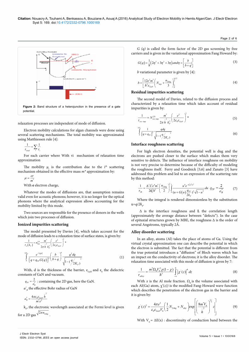
In the case of the HEMT, the juxtaposition of a wide bandgap material and a small gap material involves the creation of discontinuity of band conduction at the interface between two materials, Anderson model. In this model, at the junction of two semiconductors with different band gap, the Fermi levels are aligned. The conservation of physical parameters on both sides of the interface causes bending of the band and valence conduction, and also discontinuities at the interface of these two bands. This “heterojunction”, illustrated in Figure 2, involves the formation of a potential well in the material of small gap where to accumulate and transfer electrons from the donor layer. The heterojunction is characterized by the discontinuity of conduction
band ΔEc between the two materials [3]. This causes the accumulation of electrons in this well is called two-dimensional electron gas (2DEG: two Dimensional Electron Gas). The heterojunction allows the spatial separation of the ionized donor atoms and free electrons.
A fundamental criterion for validating such structures is of course the electron mobility of electrons in the wells that form the transistor channel.
Many mechanisms of diffusion may limit the mobility of electrons in the gas: Some are defined as elastic scattering centers (donors, interface roughness, alloy disorder, dislocations loaded) and others are inelastic (acoustic and optical phonons).
Theory and ModelThe calculation of mobility will be in what follows in the
approximation of relaxation time. This hypothesis assumes that all
AbstractThe hetero junctions GaN based offer an excellent potential for power applications at high frequency. This is due
to the important energy of the bandgap and high saturation velocity of electrons. The high mobility transistors (HEMT - High Electron Mobility Transistor) are based on the heterojunction AlGaN/GaN. Our work is the subject of an analytical study of the carrier mobility HEMTs AlGaN/GaN calculating Ionized impurities scattering, Residual impurities scattering, Interface roughness scattering, Alloy disorder scattering, dislocations scattering, Phonons and Dipoles taking into account the impact of technological parameters (doping, aluminium content) and geometric (thickness barrier, interface roughness). The results allowed us to take account of the variation of carrier density in the wells of 2D electronic gas.
Figure 1: Schematic sectional view of a HEMT AlGaN/GaN structure. The bias fields are represented. Current modulatedby the gate (G) flow through the 2D gas between the source (S) and drain (D).
Citation: Nouacry A, Touhami A, Benkassou A, Bouziane A, Aouaj A (2016) Analytical Study of Electron Mobility in Hemts Algan/Gan. J Electr Electron Syst 5: 169. doi:10.4172/2332-0796.1000169
Page 2 of 6
Volume 5 • Issue 1 • 1000169J Electr Electron SystISSN: 2332-0796 JEES an open access journal
relaxation processes are independent of mode of diffusion.
Electron mobility calculations for algan channels were done using several scattering mechanisms. The total mobility was approximated using Matthiessen rule [4]:
1 1τ τ
=∑itotal i
For each carrier where With τi mechanism of relaxation time approximation
The mobility µi is the contribution due to the ith scattering mechanism obtained in the effective mass m* approximation by:
*τµ =
em
With e electron charge,
Whatever the modes of diffusions are, that assumption remains valid even for acoustic phonons; however, it is no longer for the optical phonons where the analytical expression allows accounting for the mobility limited by this mode.
Two sources are responsible for the presence of donors in the wells which join two processes of diffusion.
Ionized impurities scattering
The model presented by Davies [4], which takes account for the mode of diffusion leads to a relaxation time of surface states, is given by:
( )
2* 22
33 0
1 *22τ ε ε
π−
=
D
impii F GaN
F
m enk h k
( )
62 2 2
20
2
1 ( 2 )
− ++ −
∫FK q d
TF
F
e b q dqb qq q G q q
K
(1)
With, d is the thickness of the barrier, εGaN and ε0 the dielectric constants of GaN and vacuum.
*
2TF
B
qa
= : containing the 2D gas, here the GaN.
a*B the effective Bohr radius of GaN
2
* 0* 2
4πε ε−
= GaNB
ham e
kF, the electronic wavelength associated at the Fermi level is given
for a 2D gas 2deg2πn.
G (q) is called the form factor of the 2D gas screening by free carriers and is given in the variational approximation Fang Howard by:
( ) ( )3 21 2 3 38
η η η η
= + + = +
bG q andb q
(3)
b variational parameter is given by [4]:1/32 *
2deg2
123ε
= +
depGaN
ne mb N (4)
Residual impurities scattering
The second model of Davies, related to the diffusion process and characterized by a relaxation time which takes account of residual impurities is given by:
2* 22
33 0
1 *22τ ε επ
−−−
=
D
res impres imp GaN
F
m eNh k
(5)
[ ]
2
20
2
1
1 ( 2 )+ −
∫FK
TF
F
qdqq q q
K (6)
Interface roughness scattering
For high electron densities, the potential well is dug and the electrons are pushed closer to the surface which makes them very sensitive to defects. The influence of interface roughness on mobility is not very precise to determine because of the difficulty of modeling the roughness itself. Ferry and Goodnick [5,6] and Zanato [3] have addressed this problem and led to an expression of the scattering rate by this method:
( )
2 2 22 12 2 4 * 42 deg
2 32 20 0
12 2 ( ) 1
2τ
− =
+ −
∆∫
Fk L u
TFIR
F
nL e m u e duqu G u uk
ò (7)
Where the integral is rendered dimonsionless by the substitution u=q/2kF.
∆ is the interface roughness and L the correlation length (approximately the average distance between “defects”). In the case of epitaxial structures grown by MBE, the roughness Δ is the order of several Angstroms, typically 2Å.
Alloy disorder scattering
In an alloy, atoms (Al) takes the place of atoms of Ga. Using the virtual crystal approximation one can describe the potential in which the electron is submitted. The fact that the potential is different from the true potential introduces a “diffusion” of Bloch waves which has an impact on the conductivity of electrons; it is the alloy disorder. The relaxation time associated with this mode of diffusion is given by 7:
0* 2 4'0 03
1 (1 ) ( )χτ
χ χ−∞
Ω −= ∫
alloy
m V z dz (8)
With x is the Al mole fraction. Ω0 is the volume associated with each Al(Ga) atom, χ’(z)) is the modified Fang-Howard wave function which describes the penetration of the electron gas in the barrier and it is given by:
12
2 *' 2 0
2 deg 20 0
4 1 8( ) exp2
πχε ε −
= +
depGaN
e m Vz N N zV h
(9)
With V0 = ∆E(x) : discontinuity of conduction band between the
Figure 2: Band structure of a heterojunction in the presence of a gate potential.

Citation: Nouacry A, Touhami A, Benkassou A, Bouziane A, Aouaj A (2016) Analytical Study of Electron Mobility in Hemts Algan/Gan. J Electr Electron Syst 5: 169. doi:10.4172/2332-0796.1000169
Page 3 of 6
Volume 5 • Issue 1 • 1000169J Electr Electron SystISSN: 2332-0796 JEES an open access journal
l’AlxGa1-xN et le GaN. V0 is the alloy scattering potential for AlGaN alloys reported ealier to be 1.8 eV [7,8]. our simulations are made from this experimental value.
Dislocations scattering
The absence of substrate adapted into mesh with GaN leads to the presence in the epitaxial layers of GaN threading dislocations. The model that can be found in the literature to allow time for mailing by dislocations is given by equation 10,11:
1* 2 2
32 22 4 0
0
1
( ) 116 ( ) 2
λτ π ε ε
−=
+ −∫L
disTFdis
GaN FF
m e duN qu uh k K (10)
Where u is defined previously by u=q/2kF. kF the Fermi wave vector which depends on the carrier density of 2D gas (n2DEG) and Ndis is the doping density of 2D dislocation lines, λL= ef/c0 where c0 is lattice constant in GaN along the direction [0001], f is the fraction of occupied acceptor states introduced by dislocation.
Phonons
The mechanism of diffusion by phonons is dominant at temperatures above 77 K for electrons, but it may be the determining factor at low temperatures in 2D structures made from particularly pure materials. We can distinguish two types of phonons (acoustic and optical).
Phonon acoustic scattering: The acoustic phonons are sound waves that alternately compress and expand the solid. The variation of lattice parameter induces a change in energy bands which will fall or rise proportionately with the constraint. Davies [4] gives a simplified expression of the relaxation time that allows a relatively easy numerical computation [9,10]. This relationship is given by:
* 2
32
1 3
16τ ρ−
= c
acs
m bkTa
v h (11)
32
* 2 2
163( )
ρµ−
= sac
c
e v hm bkTa
Where ρ the density, vs the speed of sound in the material and b is the variational parameter using the wave functions of Fang-Howard.
Optical phonons scattering: In GaN (same for AlN and InN) energy of polar optical phonons is very large and the phonon scattering is inelastic. The optical phonon energy is much larger than the thermal energy of electrons even at room temperature [11]. Thus, the majority of electrons do not have sufficient thermal energy to emit an optical phonon. Only the absorption process taking into account the relaxation time is thus reduced to the characteristic time of absorption of an optical phonon, we can then say that the emission process is effectively blocked. Gelmont [12], via this hypothesis, proposes an expression of time associated with this process.
( )2 *0 0* 2
0
( )12 ( )ω
τ ε=
op
e m N T H qq F y
(12)
With ω0 is the optical phonon frequency, *
00
2 ω= mq ħ is the optical phonon wave vector,
( )0
1exp( 1)
ω=−
N TkT
is the Bose-Einstein distribution function,
( ) 2 *2deg
11 /π−−
= + =yeF y with y n m KT
yħ , H(q0) is the form factor given by :
2 20 0
0 30
b(8b 9q b 3q )H(q )8(q b)+ +
=+
(13)
Dipoles
In heterostructures AlGaN/GaN, the presence of the electron gas can be entirely due to the polarization field as spontaneous as piezoelectric. The relaxation time attributed to this type of diffusion can be formulated by equation 13:
( )2* 222
2 3 30
2
12
1 ( 2 )τ π
=−
∫
FKD tot
dipole scrDdipole F
F
m q dqn V qk q
K (14)
is the two-dimensional Fourier transform of the scattering potential.
The density of 2D gas is the rate of aluminum given by:
2
0
13 ( )
4
=Ddipôlen
a x
Results and DiscussionThis study is based on AlGaN/GaN heterostructure whose
characteristics are given in Table 1.
Figure 3 shows for four values of electron gas density wells in the variation of mobility as a function of the the barrier thickness this structure has a typical thickness of 30 nm; the variation range was set between 1 nm and 10 nm.
For the classical values of thickness 30 nm, the mobility values are of the order of 106 cm2/Vs. This great value shows the low importance of this type of diffusion in these structures [13].
Figure 4 shows the variation of mobility attributed to such distribution as a function of the density of residual impurities for four
Nom A392χAL(%) 26dAlGaN(Å) 291NHall 300K (1012 cm-2) 7,1µHall 300K (cm2/Vs) 1734NHall 10-20K (1012 cm-2) 7,7µHall 10-20K
(cm2/Vs) 7350Buffer (µm) 1,5Subs. SiDiscloc density (cm-2) 5-7.109
Type epitaxy EJM
Table 1: Main characteristics of the sample studied.
Figure 3: Mobility limited by ionized impurities on the surface.

Citation: Nouacry A, Touhami A, Benkassou A, Bouziane A, Aouaj A (2016) Analytical Study of Electron Mobility in Hemts Algan/Gan. J Electr Electron Syst 5: 169. doi:10.4172/2332-0796.1000169
Page 4 of 6
Volume 5 • Issue 1 • 1000169J Electr Electron SystISSN: 2332-0796 JEES an open access journal
typical of 2D gas densities in our structures.
We note that the influence of residual impurities on the mobility is important for the low 2D gas densities (<5.1012 cm-2). But despite this, the mobility is always greater than an order of magnitude (for density of residual donors of about 1017 cm-3.. For high carrier densities in the well, the mobility would be really affected for doping densities above 1017 cm-3. This would allow us to conclude that this type of diffusion is not the critical factor for heterostructures where the best conductivity of gas is sought, which impose a gas density higher than 5×1012 cm-2.
According to the simulation results of Figure 5, where we note the importance of this mode of diffusion on the overall mobility of electrons in the well. The mobility varies approximately as L-2. We expect a significant drop of it depending on the length of correlation between defects [14,15]. In fact, we find that the mobility reaches a plateau which depends on the density of electrons and then practically does not vary more.
Figure 6 shows the high sensitivity of mobility to the interface quality AlGaN/GaN. The calculated values of the mobility are the same of those obtained experimentally and of the magnitude of the mobility limited by alloy disorder. The epitaxial is therefore very sensitive to this parameter that can completely degrade the mobility at low temperature (μ < 1000 cm²/Vs).
Figure 7 shows the variation of mobility as a function of electron density for three values of dislocation densities covering the range of variation for conventional structure, where f is the value unit [16].
This figure shows us that for a given dislocation density, the
electron mobility increases with the electron population in the well. This trend illustrates the screening of scattering centers as well as the population increases.
Figure 8 extends the typical dislocation density of structures encountered in the literature, the variation of mobility as a function of n2DEG for different filling factors.
The Figure 9 shows the variation of the mobility limited by acoustic phonons in the densities of electrons.
Figure 4: Mobility limited by the residual impurities.
Figure 5: Variation of mobility as a function of parameters representing the surface roughness. Δ is set at 1 Angstrom.
Figure 6: Variation of mobility according to the correlation length for ns= 0.1, 0.5 and 1.1013cm-2.Δis set at Angstrom.
Figure 7: Variation of mobility depending on the density of 2D gas.
Figure 8: Influence of load factor on the mobility of dislocations.

Citation: Nouacry A, Touhami A, Benkassou A, Bouziane A, Aouaj A (2016) Analytical Study of Electron Mobility in Hemts Algan/Gan. J Electr Electron Syst 5: 169. doi:10.4172/2332-0796.1000169
Page 5 of 6
Volume 5 • Issue 1 • 1000169J Electr Electron SystISSN: 2332-0796 JEES an open access journal
In Figure 10, we find that at room temperature, the mobility is limited by optical phonons.
In Figure 11 we plot the dipole scattering limited mobility as a function of 2DEG sheet density. this characteristic represents a minimum to a 2DEG density between 20-30×1012 cm-2.
We note that the values of mobility are far greater than the maximum mobility obtained for such structures, indicating that it is not at this stage of device development, the critical factor in mobility is achieved.
Figure 9: Variation of the mobility limited by acoustic phonons as a function of the density of 2D gas.
Figure 10: Variation of the mobility limited by optical phonons depending on the density of 2D gas.
Figure 11: Mobility function of the density nsin the case of scattering by dipoles.
Figure 12: Variation of mobility in the electrons density calculates and experimental.
Figure 12 shows the variation of total mobility (as considering the impact of these broadcasts) calculated a function of densities of electron and operating temperature of 300 K. The curves show that the alloy scattering effect is high for electron densities ranging from 3-5×1012 cm-2. Furthermore, the simulation results are close to those experimental.
Conclusion The analytical study of the behavior of the mobility of the HEMT
structure and its dependency on the density of 2D gas, allowed us to account for the variation of carrier density in the electronic wells of 2D gas.
At room temperature, the strong involvement of optical phonons is the limiting factor mobility. By adjusting the alloy disorder, surface roughness and dislocation density, one can earn a few hundred cm²/Vs, while increasing the carrier density and consequently the conductivity of the channel.
We can conclude that the alloy disorder plays an important role for the values of electron density that is of the order of 1013 cm-2. This work will enable us to improve the technology of HEMT structure and modeling the transfer characteristic I - V of transistor into static. This will inject the value of mobility as a function of gate voltage. Hence, it allows us to be able of knowing the curve μ (nDEG).
References
1. Baliga B (1996) Trends in power semiconductor devices. IEEE Transactions on Electron Devices 43: 1717-1731.
2. Vellas N (2003) Power results at 4 GHz of AlGaN–GaN HEMTs on high resistive silicon (111) substrate IEEE Microwave Wireless Comp. Lett 13: 99-101.
3. Davies JH (1998) The physics of low dimensional semiconductors: An introduction.
4. Ferry DK, Goodnick SM (1997) Transport in nanostructures.
5. Zanato D, Gokden S, Balkan N, Ridley BK (2004) The effect of interface roughness and dislocation scattering on low temperature mobility of 2D electron gas in GaN/AlGaN. Semicond Sci Technol 19: 427-432.
6. Hsu L, Walukiewicz W (1997) Electron mobility in AlxGa1-xN/GaN heterostructures. PRB 56: 1520-1528.
7. Jena D (2003) Polarization induced electron populations in III-V nitride semiconductors Transport, growth, and device applications.
8. Farvacque JL, Bougrioua Z, Moerman I (2001) Free-carrier mobility in GaN in the presence of dislocation walls. PRB 63: 115-202.
9. Zhao D, Kuhn K (1991) Dislocation scattering in n type modulation doped AlGaAs/InGaAs/AlGaAs quantum wells. IEEE trans Elect Dev 38: 2582-2589.

Citation: Nouacry A, Touhami A, Benkassou A, Bouziane A, Aouaj A (2016) Analytical Study of Electron Mobility in Hemts Algan/Gan. J Electr Electron Syst 5: 169. doi:10.4172/2332-0796.1000169
Page 6 of 6
Volume 5 • Issue 1 • 1000169J Electr Electron SystISSN: 2332-0796 JEES an open access journal
10. Jena D, Gossard AC, Mishra UK (2000) Dislocation scattering in atwodimensional electron gas. APL 76: 1707-1709.
11. Gelmont BL, Shur M, Stroscio M (1995) Polar optical-phonon scattering in three and two dimensional electron gases. J Appl Phys 77: 657-660.
12. Jena D, Gossard AC, Mishra UK (2000) Dipole scattering in polarizationinduced III–V nitride two-dimensional electron gases. J Appl Phys 88: 4734-4738.
13. Bougrioua Z (2003) Engineering of an Insulating Buffer and Use of AlN
interlayers: Two optimisations for AlGaN-GaN HEMT-like structures. Phys Stat 195: 93.
14. Farvacque JL, Bougrioua Z (2003) Carrier mobility versus carrier density inAlxGa1-xN/GaNquantum wells.
15. Lorenzini P (2004) Caractérisations des hétérostructures AlGaN/GaN: Despropriétés de transport aux transistors à haute mobilité HEMT.
16. Jena D, Arthur CG, Mishra UK (2000) Dipole scattering in polarization induced III–V nitride two-dimensional electron gases. J Appl Phys 88: 4734-4738.