current interactions mitigation in 3-phase pfc modular
TRANSCRIPT

applied sciences
Article
Current Interactions Mitigation in 3-Phase PFC Modular Rectifierthrough Differential-Mode Choke Filter Boost Converter
José Teixeira Gonçalves 1,* , Stanimir Valtchev 1,* and Rui Melicio 2,3
Citation: Gonçalves, J.T.; Valtchev, S.;
Melicio, R. Current Interactions
Mitigation in 3-Phase PFC Modular
Rectifier through Differential-Mode
Choke Filter Boost Converter. Appl.
Sci. 2021, 11, 1684. https://doi.org/
10.3390/app11041684
Academic Editors: Radu Godina,
Edris Pouresmaeil and Eduardo M.
G. Rodrigues
Received: 30 December 2020
Accepted: 9 February 2021
Published: 13 February 2021
Publisher’s Note: MDPI stays neutral
with regard to jurisdictional claims in
published maps and institutional affil-
iations.
Copyright: © 2021 by the authors.
Licensee MDPI, Basel, Switzerland.
This article is an open access article
distributed under the terms and
conditions of the Creative Commons
Attribution (CC BY) license (https://
creativecommons.org/licenses/by/
4.0/).
1 Departamento de Engenharia Eletrotécnica e Computador, CTS/UNINOVA, FCT,Universidade NOVA de Lisboa, 2829-516 Monte Caparica, Portugal
2 IDMEC, Instituto Superior Técnico, Universidade de Lisboa, Av. Rovisco Pais 1, 1049-001 Lisboa, Portugal;[email protected]
3 ICT, Escola de Ciências e Tecnologia, Universidade de Évora, Rua Romão Ramalho 59, 7002-554 Évora, Portugal* Correspondence: [email protected] (J.T.G.); [email protected] (S.V.)
Abstract: In this paper, a new way to mitigate the current interactions is proposed. The problemof current interactions arises when a modular three-phase (3-phase) rectifier (three single-phasemodules) with boost converter for power factor correction (PFC) is used. A new differential-modechoke filter is implemented in the developed boost converter. The choke here is a specially madedifferential inductor in the input of the boost converter that eliminates the known current interactions.To prove the new concept, a study of the level of mitigation of the current interactions is presented.The control is operated in continuous driving mode (CCM), and the popular UC3854B circuit wasused for this. The rectifier proposal is validated through a set of simulations performed on the PSIM12.0 platform, as well as the construction of a prototype. With the results obtained, it is confirmed thatthe differential-mode choke filter eliminates the current interactions. It is observed that at the inputof the rectifier, a sinusoidal alternating current with a low level of harmonic distortion is consumedfrom the grid. The sinusoidal shape of the phase current proves that a better power factor capable ofmeeting the international standards is obtained, and that the circuit in its initial version is operational.This proven result promises a good PFC operation, to guarantee the better quality of the electricalenergy, being able to be applied in systems that require a high PFC, e.g., in battery charging, windsystems, or in aeronautics and spacecrafts.
Keywords: three-phase rectifier; boost converter; interactions; differential-mode choke filter; windenergy; aeronautics and spacecrafts
1. Introduction
Most electrical loads use direct current (DC) electrical energy, which implies the useof a rectifier that converts alternating current (AC) electrical energy to DC, which is alsoknown as a static rectifier. The rectifier was widely developed thanks to the emergenceof semiconductor devices as diodes (1900s) and transistors (1950s) a story told alreadyin [1]. There are several types of AC–DC converters (rectifiers) prepared for various loads.The character of the load depends on the respective need and the cost associated with therectifier. Briefly, rectifiers are classified into two groups, bidirectional and unidirectional.
The bidirectional rectifiers are usually formed by a Graetz bridge (single-phase orthree-phase) with transistors (MOSFETs, IGBTs, etc.), thus requiring a control circuit todrive the transistors. They are often used as a first stage for an AC–DC–AC converter, whenafter the rectifier the goal is to inject energy to the grid. As an example, some wind turbinesapply this double conversion for producing the final AC power [2–4] or in aeronauticalapplications [5].
The unidirectional rectifiers use diodes as a switching device in most of the cases.There are other unidirectional rectifiers, implemented as switching converters, but theyown the possibility to be reformatted into bidirectional ones. The diodes and thyristors are
Appl. Sci. 2021, 11, 1684. https://doi.org/10.3390/app11041684 https://www.mdpi.com/journal/applsci

Appl. Sci. 2021, 11, 1684 2 of 19
naturally commutated by the periodic changes of the polarity of the AC supply voltage.These rectifiers are also commonly constructed as Graetz bridges of diodes, single-phase orthree-phase ones. The diodes Graetz bridges are more attractive, as they are simple, robust,reliable, and low-cost rectifiers when compared to the to the bidirectional rectifiers or anysophisticated AC–DC switching converters. Single-phase rectifiers are used for loads thatdemand lower power, and some of them are coupled to a converter in order to reducethe disturbances that the rectifier can inject into the electrical network. The three-phaserectifiers, on the other hand, cause great disturbance in the electrical network, due to thelarge amount of power demanded by the load and its nature (usually inductive, sometimescapacitive and nonlinear loads), compromising the quality of the energy in the electricalnetwork [1]. Therefore, in order to dimension the three-phase rectifiers, some importantparameters must be analyzed, being the rectifier and the interface between the grid and theload [6]. Briefly, the following criteria are most important:
Criteria for connecting correctly the rectifier to the grid:
• Voltage level and its variation;• Nominal frequency and its variation;• Minimum power factor (PF) value allowed by the energy supplier;• Harmonic distortion level that the energy supplier allows.
Criteria for connecting the rectifier to the load:
• Nominal voltage and respective operating current variation;• Maximum allowed ripple of voltage and current;• Accurate and reliable regulation of the current and voltage, as the load requires.
Additional criteria:
• Efficiency;• Guarantee of reliability;• Acceptable physical and mechanical parameters (weight, volume, temperature).
The drawback of the unidirectional diode or thyristor rectifiers is the high totalharmonic distortion (THD) that it injects into the electric grid and the low total powerfactor (PF) value. With this, the rectifier compromises the quality of energy in the electricalnetwork. As a way of safeguarding and control of the quality of energy in the electricgrid, some standards are emerging. Examples of international standards used on energyquality are IEC61000-3-2 and IEC61000-3-4, and for the THD of the current injected into theelectrical network, IEEE Std 519-2014 is used.
As a way to use the more sophisticated unidirectional rectifiers in the electric networks,some versions of them are aimed to improve the total harmonic distortion (THD). It canbe seen in Figure 1 that some rectifiers are power factor correctors (PFC), keeping theTHD as low as possible, complying with the established standards [7,8]. In most cases,another converter is associated with the rectifier, to control the current. There is also thepossibility to associate an active power filter to the rectifier’s input terminals, in order tocompensate the currents generated by the rectifier, thus obtaining a good quality sinusoidalcurrent [9,10] at the rectifier input. Some studies are focused on improving the efficiency ofthe active power filter and simplifying the control system, as in [10]. Other studies focuson implementing the hysteresis, called also Bang-Bang control [11].
In this case study, the modular three-phase rectifiers associated with a boost converterwill be analyzed, as this combination improves the power factor (PF). This effect is achievedby shaping the input currents sinusoidally, thus guaranteeing a minimum THD at the input.

Appl. Sci. 2021, 11, 1684 3 of 19Appl. Sci. 2021, 11, x FOR PEER REVIEW 3 of 20
Figure 1. Three-phase hybrid rectifiers types [7,8].
In this case study, the modular three-phase rectifiers associated with a boost con-
verter will be analyzed, as this combination improves the power factor (PF). This effect is
achieved by shaping the input currents sinusoidally, thus guaranteeing a minimum THD
at the input.
1.1. Three-Phase Modular Rectifiers with Boost Converter
The three-phase modular rectifiers with additional converter are usually composed
of three single-phase modules, where each module controls its phase individually. In the
numerous configurations that can be created, the single-phase rectifiers interact with each
other, which eliminates the possibility of control by the involved boost converter [12–14].
This becomes a problem, since the purpose of the individual rectifiers is to control the
current independently and to obtain a sinusoidal current with low THD and high PF in
each phase. There are some three-phase modular rectifiers that were created with the abil-
ity to eliminate those current interactions. Here, some more relevant rectifiers are sug-
gested by this paper.
A simple way to solve the current interaction problem in a modular three-phase rec-
tifier is analyzed in [15,16]. In this work, the author was concerned with the avoiding the
interaction between the phase input currents of the rectifier. For this, a transformer is im-
plemented at the input of each single-phase rectifier. This isolation by transformers makes
the interaction current stay in the secondary circuit of each rectifier and is not seen as
effect in the primary circuit. The primary currents and the sensors to control them do not
see any disturbance then. In this case, the PFC is working correctly but at the expense of
transformers application. The problem with this solution is that the transformers are grid
frequency type, and this, depending on the power of the rectifier, obliges them to be
heavy, bulky, and expensive.
In [17–19], to eliminate the current interaction, the author implemented yet another
diode at the output of the negative pole of each boost converter. This diode is polarized
inversely to the direction of the interaction current. An inductor at the negative terminal
of the input of each boost converter do the rest of the job. The inductor of a classic boost
converter in this case is split in two, one in the positive pole and one in the negative pole.
The mitigation of the interaction occurs because the impedance of the inductor is high
(due to the switching frequency) and therefore blocks the interaction current. Another
method similar to this one but with a slight difference is presented in [20,21]. In this
method, the two inductors of the boost converter are replaced by a coil winding inductor
coupled to increase the inductance effect by a factor 4, as it is calculated there. By this
special double-windings inductor, the filtering effect better eliminates the possible inter-
actions. The problem of this last solution [20,21] is the increased danger of the possible
saturation of the inductor, since it is a coupled inductor with concordant windings.
Figure 1. Three-phase hybrid rectifiers types [7,8].
1.1. Three-Phase Modular Rectifiers with Boost Converter
The three-phase modular rectifiers with additional converter are usually composedof three single-phase modules, where each module controls its phase individually. In thenumerous configurations that can be created, the single-phase rectifiers interact with eachother, which eliminates the possibility of control by the involved boost converter [12–14].This becomes a problem, since the purpose of the individual rectifiers is to control the currentindependently and to obtain a sinusoidal current with low THD and high PF in each phase.There are some three-phase modular rectifiers that were created with the ability to eliminatethose current interactions. Here, some more relevant rectifiers are suggested by this paper.
A simple way to solve the current interaction problem in a modular three-phaserectifier is analyzed in [15,16]. In this work, the author was concerned with the avoidingthe interaction between the phase input currents of the rectifier. For this, a transformeris implemented at the input of each single-phase rectifier. This isolation by transformersmakes the interaction current stay in the secondary circuit of each rectifier and is not seenas effect in the primary circuit. The primary currents and the sensors to control them donot see any disturbance then. In this case, the PFC is working correctly but at the expenseof transformers application. The problem with this solution is that the transformers aregrid frequency type, and this, depending on the power of the rectifier, obliges them to beheavy, bulky, and expensive.
In [17–19], to eliminate the current interaction, the author implemented yet anotherdiode at the output of the negative pole of each boost converter. This diode is polarizedinversely to the direction of the interaction current. An inductor at the negative terminalof the input of each boost converter do the rest of the job. The inductor of a classic boostconverter in this case is split in two, one in the positive pole and one in the negative pole.The mitigation of the interaction occurs because the impedance of the inductor is high (dueto the switching frequency) and therefore blocks the interaction current. Another methodsimilar to this one but with a slight difference is presented in [20,21]. In this method, thetwo inductors of the boost converter are replaced by a coil winding inductor coupledto increase the inductance effect by a factor 4, as it is calculated there. By this specialdouble-windings inductor, the filtering effect better eliminates the possible interactions.The problem of this last solution [20,21] is the increased danger of the possible saturationof the inductor, since it is a coupled inductor with concordant windings.
Another possibility is also presented in [1], where the author replaces the inductorof the boost converter with a coupled inductor of discordant windings in each converterand implements a diode at the output of the negative pole of each converter. The coupledinductor implemented in addition to the boost inductor introduces impedance differences.The impedance in the direction of the interaction current is much higher than the impedancein the direction of the normal current; thus, the circuit functions as an additional filter forthe interaction current. This solution [1] shows good results. One technology problem isthe winding of the inductor core, since the coupled inductor must block the passage of the

Appl. Sci. 2021, 11, 1684 4 of 19
interaction current and let the normal current pass. These inductors are not easy to findready to be supplied and require a special attention.
1.2. Problem and Objectives
As already seen, there are some techniques to mitigate current interactions in modularthree-phase rectifiers with boost converter and PFC, some of which stand out better thanothers. The problem is that these techniques to mitigate current interactions have somecharacteristics that may be undesirable, such as the increase in volume, weight, saturation,and constructive complexity.
To solve these problems (volume, weight, saturation, and constructive complexity),it is proposed to introduce DMCF in each boost converter (between the inductor and theswitching transistor) of the modular three-phase rectifier, to filter the current interactions.In the same way, isolate the supply circuit with the control circuit as much as possible usingthe interface circuit, but without losing simultaneous operation.
The general objective of this work is to propose a modular three-phase rectifier (threemodules) with boost converters and power factor correction capable of mitigating currentinteractions through the DMCF. To achieve the general objective, it is essential to outlinethe specific objectives. Thus, the specific objectives to be achieved are as follows:
• Demonstrate that the DMCF is capable of mitigating the current interaction thatappears in three-phase modular rectifiers (three modules) with boost converters andpower factor correction;
• Show that the interface circuit is able to isolate the power circuit with the controlcircuit in order to avoid current interactions;
• Enable other researchers to replicate the proposed circuit by simulation and prove itsfunctionality or develop improvements.
2. Design Proposal of the Three-Phase Modular Rectifier2.1. Proposal of Three-Phase Modular Rectifier
The proposed three-phase modular rectifier is illustrated in Figure 2. It is composedof three single-phase rectifier modules, each of which is connected to a boost converterwith control in the CCM. The connection of the rectifier to the grid can be made in star (Y)or delta (∆) configuration. Here, in this particular case, it will be dealt with the star (Y)connection. This proposed rectifier has the purpose of rectifying a three-phase alternatingcurrent, producing a direct current with stable output voltage. A high PF and low THD isexpected, thanks to the implementation of the differential-mode choke filter (DMCF) asa part of the boost converter. This DMCF can be implemented before or after the boostconverter inductor.
Appl. Sci. 2021, 11, x FOR PEER REVIEW 5 of 20
Figure 2. Proposal of three-phase modular rectifier.
2.2. Operating Principle of the Proposed Rectifier
This rectifier is developed precisely to work with voltage and three-phase current of
sinusoidal signal, expressed by:
𝑉𝑖𝑛𝑎(𝑡) = 𝑉𝑝 𝑆𝑖𝑛(𝑤𝑡)
𝑉𝑖𝑛𝑏(𝑡) = 𝑉𝑝 𝑆𝑖𝑛(𝑤𝑡 − 120)
𝑉𝑖𝑛𝑐(𝑡) = 𝑉𝑝 𝑆𝑖𝑛(𝑤𝑡 + 120)
(1)
Here 𝑉𝑖𝑛𝑎 , 𝑉𝑖𝑛𝑏 , 𝑉𝑖𝑛𝑐 is the voltage in phase a, b, and c; 𝑉𝑝 is the peak voltage.
The operating principle is based on Figure 2. In Figure 2, it is seen that the power
supplied by the source is distributed over three paths, since the modular three-phase rec-
tifier is composed of three rectifiers. The analysis can also be done through the input cur-
rents, 𝑖𝑖𝑛𝑎 , 𝑖𝑖𝑛𝑏 , 𝑎𝑛𝑑 𝑖𝑖𝑛𝑐, which will be distributed to the three rectifiers consecutively and
can be calculated by:
𝑖𝑖𝑛𝑎(𝑡) =
2
3 𝑃𝑜𝑉𝑝 𝑆𝑖𝑛 (𝑤𝑡)
𝑖𝑖𝑛𝑏(𝑡) =2
3 𝑃𝑜𝑉𝑝 𝑆𝑖𝑛 (𝑤𝑡 − 120)
𝑖𝑖𝑛𝑐(𝑡) =2
3 𝑃𝑜𝑉𝑝 𝑆𝑖𝑛 (𝑤𝑡 + 120)
(2)
Here 𝑖𝑖𝑛𝑎 , 𝑖𝑖𝑛𝑏 , 𝑖𝑖𝑛𝑐 is the input current in phases a, b, and c, and 𝑃𝑜 is the output
power.
Each current will thus be rectified by its corresponding rectifier composed of a bridge
of four diodes, after which a DMCF has been implemented to the respective boost con-
verter. The DMCF and the boost stage are there in order to eliminate the current interac-
tions (as is explained later in Section 2.3), and to serve the purpose of producing at the
input of the rectifier a sinusoidal waveform of the phase current. The current is produced
in phase with the voltage, thus guaranteeing a high PF and a low THD. Each rectifier
connected to its boost converter thus produces an output current 𝐼𝑜1, 𝐼𝑜2 , and 𝐼𝑜3, respec-
tively, which will then be added together, thus obtaining the output current 𝐼𝑜 for charg-
ing the output capacitor, which acts as a filter and supplies the total current to the load.
The current that charges the filter capacitor varies its amplitude, but the output voltage
remains stable. As the converter is a boost converter, the output voltage will be higher
than the input voltage.
The total input power can be given by:
Figure 2. Proposal of three-phase modular rectifier.
Appl. Sci. 2021, 11, 1684 5 of 19
2.2. Operating Principle of the Proposed Rectifier
This rectifier is developed precisely to work with voltage and three-phase current ofsinusoidal signal, expressed by:
Vina(t) = Vp Sin(wt)Vinb(t) = Vp Sin(wt − 120)
Vinc(t) = Vp Sin(wt + 120)(1)
Here Vina, Vinb, Vinc is the voltage in phase a, b, and c; Vp is the peak voltage.The operating principle is based on Figure 2. In Figure 2, it is seen that the power
supplied by the source is distributed over three paths, since the modular three-phaserectifier is composed of three rectifiers. The analysis can also be done through the inputcurrents, iina, iinb, and iinc, which will be distributed to the three rectifiers consecutivelyand can be calculated by:
iina(t) = 23
PoVp
Sin (wt)
iinb(t) = 23
PoVp
Sin (wt − 120)
iinc(t) = 23
PoVp
Sin (wt + 120)
(2)
Here iina, iinb, iinc is the input current in phases a, b, and c, and Po is the output power.Each current will thus be rectified by its corresponding rectifier composed of a bridge
of four diodes, after which a DMCF has been implemented to the respective boost converter.The DMCF and the boost stage are there in order to eliminate the current interactions (as isexplained later in Section 2.3), and to serve the purpose of producing at the input of therectifier a sinusoidal waveform of the phase current. The current is produced in phasewith the voltage, thus guaranteeing a high PF and a low THD. Each rectifier connected toits boost converter thus produces an output current Io1, Io2, and Io3, respectively, whichwill then be added together, thus obtaining the output current Io for charging the outputcapacitor, which acts as a filter and supplies the total current to the load. The current thatcharges the filter capacitor varies its amplitude, but the output voltage remains stable. Asthe converter is a boost converter, the output voltage will be higher than the input voltage.
The total input power can be given by:
Pin = 3Vp Ip
2= Vo Io (3)
Ip =2 Vo Io
3 Vo(4)
Here, Pin is the input power, Ip is the peak current value, Vp is the peak voltage, Vo isthe converter output voltage, and Io is the output current.
2.3. Mitigation of Current Interaction
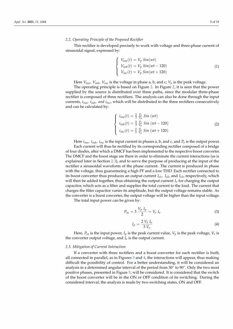
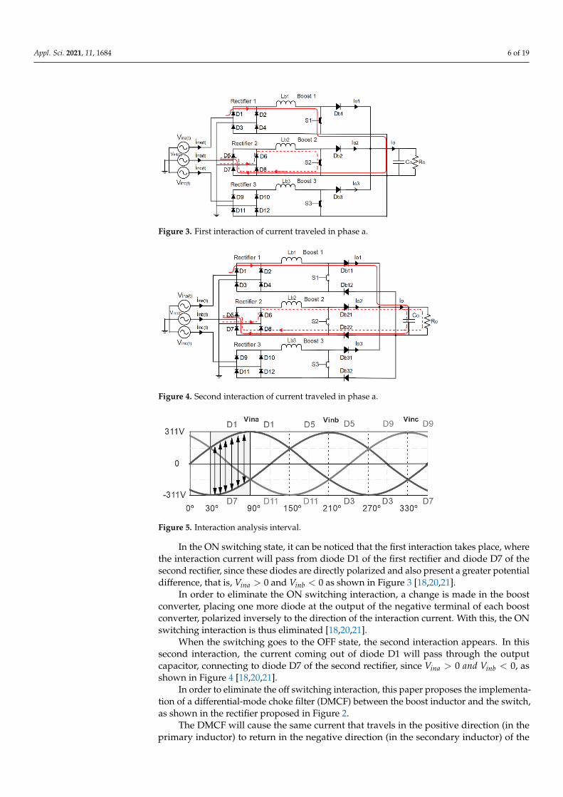
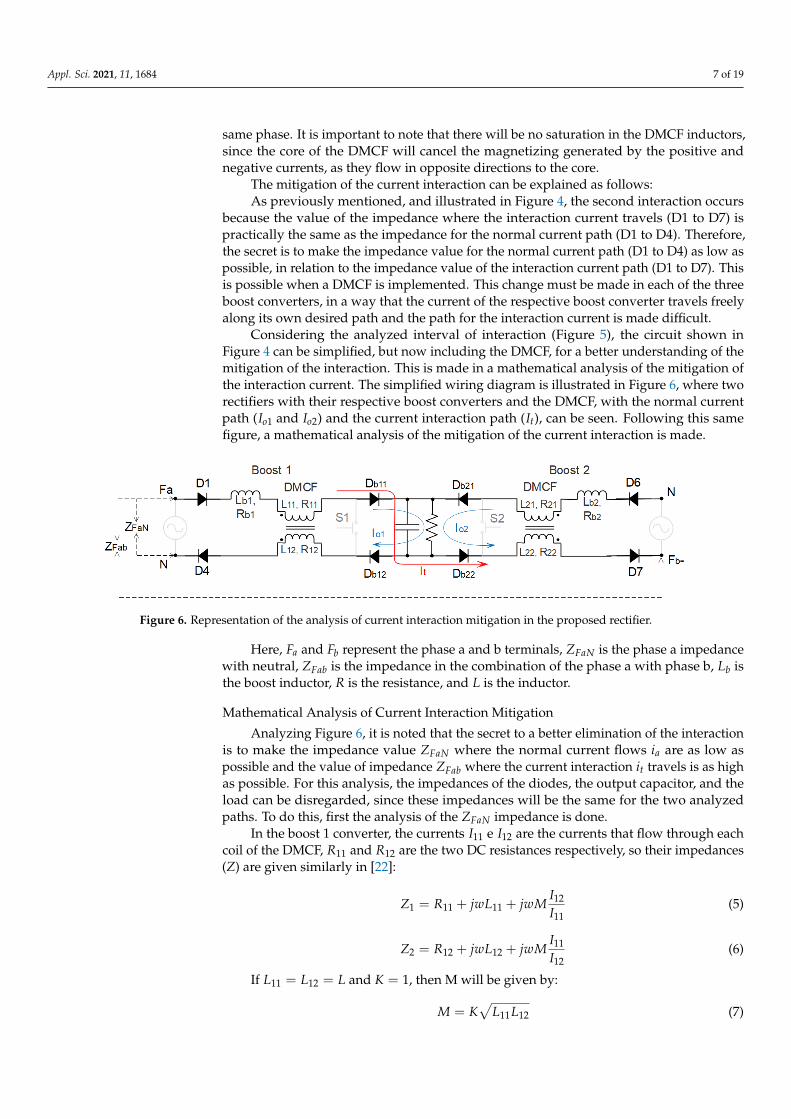
If a converter with three rectifiers and a boost converter for each rectifier is built,all connected in parallel, as in Figures 3 and 4, the interactions will appear, thus makingdifficult the possibility of control. For a better understanding, it will be considered ananalysis in a determined angular interval of the period from 30 to 90. Only the two mostpositive phases, presented in Figure 5, will be considered. It is considered that the switchof the boost converter will be in the ON or OFF condition of its switching. During theconsidered interval, the analysis is made by two switching states, ON and OFF.
Appl. Sci. 2021, 11, 1684 6 of 19
Appl. Sci. 2021, 11, x FOR PEER REVIEW 6 of 20
𝑃𝑖𝑛 = 3 𝑉𝑝 𝐼𝑝
2= 𝑉𝑜 𝐼𝑜 (3)
𝐼𝑝 =2 𝑉𝑜 𝐼𝑜3 𝑉𝑜
(4)
Here, 𝑃𝑖𝑛 is the input power, 𝐼𝑝 is the peak current value, 𝑉𝑝 is the peak voltage, 𝑉𝑜
is the converter output voltage, and 𝐼𝑜 is the output current.
2.3. Mitigation of Current Interaction
If a converter with three rectifiers and a boost converter for each rectifier is built, all
connected in parallel, as in Figures 3 and 4, the interactions will appear, thus making dif-
ficult the possibility of control. For a better understanding, it will be considered an analy-
sis in a determined angular interval of the period from 30° to 90°. Only the two most pos-
itive phases, presented in Figure 5, will be considered. It is considered that the switch of
the boost converter will be in the ON or OFF condition of its switching. During the con-
sidered interval, the analysis is made by two switching states, ON and OFF.
Figure 3. First interaction of current traveled in phase a.
Figure 4. Second interaction of current traveled in phase a.
Figure 5. Interaction analysis interval.
Figure 3. First interaction of current traveled in phase a.
Appl. Sci. 2021, 11, x FOR PEER REVIEW 6 of 20
𝑃𝑖𝑛 = 3 𝑉𝑝 𝐼𝑝
2= 𝑉𝑜 𝐼𝑜 (3)
𝐼𝑝 =2 𝑉𝑜 𝐼𝑜3 𝑉𝑜
(4)
Here, 𝑃𝑖𝑛 is the input power, 𝐼𝑝 is the peak current value, 𝑉𝑝 is the peak voltage, 𝑉𝑜
is the converter output voltage, and 𝐼𝑜 is the output current.
2.3. Mitigation of Current Interaction
If a converter with three rectifiers and a boost converter for each rectifier is built, all
connected in parallel, as in Figures 3 and 4, the interactions will appear, thus making dif-
ficult the possibility of control. For a better understanding, it will be considered an analy-
sis in a determined angular interval of the period from 30° to 90°. Only the two most pos-
itive phases, presented in Figure 5, will be considered. It is considered that the switch of
the boost converter will be in the ON or OFF condition of its switching. During the con-
sidered interval, the analysis is made by two switching states, ON and OFF.
Figure 3. First interaction of current traveled in phase a.
Figure 4. Second interaction of current traveled in phase a.
Figure 5. Interaction analysis interval.
Figure 4. Second interaction of current traveled in phase a.
Appl. Sci. 2021, 11, x FOR PEER REVIEW 6 of 20
𝑃𝑖𝑛 = 3 𝑉𝑝 𝐼𝑝
2= 𝑉𝑜 𝐼𝑜 (3)
𝐼𝑝 =2 𝑉𝑜 𝐼𝑜3 𝑉𝑜
(4)
Here, 𝑃𝑖𝑛 is the input power, 𝐼𝑝 is the peak current value, 𝑉𝑝 is the peak voltage, 𝑉𝑜
is the converter output voltage, and 𝐼𝑜 is the output current.
2.3. Mitigation of Current Interaction
If a converter with three rectifiers and a boost converter for each rectifier is built, all
connected in parallel, as in Figures 3 and 4, the interactions will appear, thus making dif-
ficult the possibility of control. For a better understanding, it will be considered an analy-
sis in a determined angular interval of the period from 30° to 90°. Only the two most pos-
itive phases, presented in Figure 5, will be considered. It is considered that the switch of
the boost converter will be in the ON or OFF condition of its switching. During the con-
sidered interval, the analysis is made by two switching states, ON and OFF.
Figure 3. First interaction of current traveled in phase a.
Figure 4. Second interaction of current traveled in phase a.
Figure 5. Interaction analysis interval. Figure 5. Interaction analysis interval.
In the ON switching state, it can be noticed that the first interaction takes place, wherethe interaction current will pass from diode D1 of the first rectifier and diode D7 of thesecond rectifier, since these diodes are directly polarized and also present a greater potentialdifference, that is, Vina > 0 and Vinb < 0 as shown in Figure 3 [18,20,21].
In order to eliminate the ON switching interaction, a change is made in the boostconverter, placing one more diode at the output of the negative terminal of each boostconverter, polarized inversely to the direction of the interaction current. With this, the ONswitching interaction is thus eliminated [18,20,21].
When the switching goes to the OFF state, the second interaction appears. In thissecond interaction, the current coming out of diode D1 will pass through the outputcapacitor, connecting to diode D7 of the second rectifier, since Vina > 0 and Vinb < 0, asshown in Figure 4 [18,20,21].
In order to eliminate the off switching interaction, this paper proposes the implementa-tion of a differential-mode choke filter (DMCF) between the boost inductor and the switch,as shown in the rectifier proposed in Figure 2.
The DMCF will cause the same current that travels in the positive direction (in theprimary inductor) to return in the negative direction (in the secondary inductor) of the
Appl. Sci. 2021, 11, 1684 7 of 19
same phase. It is important to note that there will be no saturation in the DMCF inductors,since the core of the DMCF will cancel the magnetizing generated by the positive andnegative currents, as they flow in opposite directions to the core.
The mitigation of the current interaction can be explained as follows:As previously mentioned, and illustrated in Figure 4, the second interaction occurs
because the value of the impedance where the interaction current travels (D1 to D7) ispractically the same as the impedance for the normal current path (D1 to D4). Therefore,the secret is to make the impedance value for the normal current path (D1 to D4) as low aspossible, in relation to the impedance value of the interaction current path (D1 to D7). Thisis possible when a DMCF is implemented. This change must be made in each of the threeboost converters, in a way that the current of the respective boost converter travels freelyalong its own desired path and the path for the interaction current is made difficult.
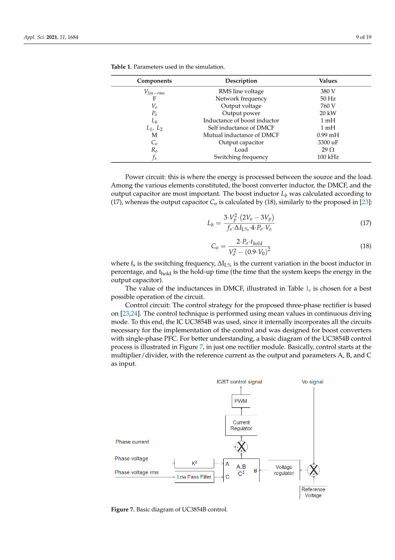
Considering the analyzed interval of interaction (Figure 5), the circuit shown inFigure 4 can be simplified, but now including the DMCF, for a better understanding of themitigation of the interaction. This is made in a mathematical analysis of the mitigation ofthe interaction current. The simplified wiring diagram is illustrated in Figure 6, where tworectifiers with their respective boost converters and the DMCF, with the normal currentpath (Io1 and Io2) and the current interaction path (It), can be seen. Following this samefigure, a mathematical analysis of the mitigation of the current interaction is made.
Appl. Sci. 2021, 11, x FOR PEER REVIEW 7 of 20
In the ON switching state, it can be noticed that the first interaction takes place, where
the interaction current will pass from diode D1 of the first rectifier and diode D7 of the
second rectifier, since these diodes are directly polarized and also present a greater poten-
tial difference, that is, 𝑉𝑖𝑛𝑎 > 0 and 𝑉𝑖𝑛𝑏 < 0 as shown in Figure 3 [18,20,21].
In order to eliminate the ON switching interaction, a change is made in the boost
converter, placing one more diode at the output of the negative terminal of each boost
converter, polarized inversely to the direction of the interaction current. With this, the ON
switching interaction is thus eliminated [18,20,21].
When the switching goes to the OFF state, the second interaction appears. In this
second interaction, the current coming out of diode D1 will pass through the output ca-
pacitor, connecting to diode D7 of the second rectifier, since 𝑉𝑖𝑛𝑎 > 0 𝑎𝑛𝑑 𝑉𝑖𝑛𝑏 < 0, as
shown in Figure 4 [18,20,21].
In order to eliminate the off switching interaction, this paper proposes the implemen-
tation of a differential-mode choke filter (DMCF) between the boost inductor and the
switch, as shown in the rectifier proposed in Figure 2.
The DMCF will cause the same current that travels in the positive direction (in the
primary inductor) to return in the negative direction (in the secondary inductor) of the
same phase. It is important to note that there will be no saturation in the DMCF inductors,
since the core of the DMCF will cancel the magnetizing generated by the positive and
negative currents, as they flow in opposite directions to the core.
The mitigation of the current interaction can be explained as follows:
As previously mentioned, and illustrated in Figure 4, the second interaction occurs
because the value of the impedance where the interaction current travels (D1 to D7) is
practically the same as the impedance for the normal current path (D1 to D4). Therefore,
the secret is to make the impedance value for the normal current path (D1 to D4) as low
as possible, in relation to the impedance value of the interaction current path (D1 to D7).
This is possible when a DMCF is implemented. This change must be made in each of the
three boost converters, in a way that the current of the respective boost converter travels
freely along its own desired path and the path for the interaction current is made difficult.
Considering the analyzed interval of interaction (Figure 5), the circuit shown in Fig-
ure 4 can be simplified, but now including the DMCF, for a better understanding of the
mitigation of the interaction. This is made in a mathematical analysis of the mitigation of
the interaction current. The simplified wiring diagram is illustrated in Figure 6, where two
rectifiers with their respective boost converters and the DMCF, with the normal current
path (𝐼𝑜1 and 𝐼𝑜2) and the current interaction path (𝐼𝑡), can be seen. Following this same
figure, a mathematical analysis of the mitigation of the current interaction is made.
Figure 6. Representation of the analysis of current interaction mitigation in the proposed rectifier.
Here, 𝐹𝑎 and 𝐹𝑏 represent the phase a and b terminals, 𝑍𝐹𝑎𝑁 is the phase a imped-
ance with neutral, 𝑍𝐹𝑎𝑏 is the impedance in the combination of the phase a with phase b,
𝐿𝑏 is the boost inductor, 𝑅 is the resistance, and 𝐿 is the inductor.
Figure 6. Representation of the analysis of current interaction mitigation in the proposed rectifier.
Here, Fa and Fb represent the phase a and b terminals, ZFaN is the phase a impedancewith neutral, ZFab is the impedance in the combination of the phase a with phase b, Lb isthe boost inductor, R is the resistance, and L is the inductor.
Mathematical Analysis of Current Interaction Mitigation
Analyzing Figure 6, it is noted that the secret to a better elimination of the interactionis to make the impedance value ZFaN where the normal current flows ia are as low aspossible and the value of impedance ZFab where the current interaction it travels is as highas possible. For this analysis, the impedances of the diodes, the output capacitor, and theload can be disregarded, since these impedances will be the same for the two analyzedpaths. To do this, first the analysis of the ZFaN impedance is done.
In the boost 1 converter, the currents I11 e I12 are the currents that flow through eachcoil of the DMCF, R11 and R12 are the two DC resistances respectively, so their impedances(Z) are given similarly in [22]:
Z1 = R11 + jwL11 + jwMI12
I11(5)
Z2 = R12 + jwL12 + jwMI11
I12(6)
If L11 = L12 = L and K = 1, then M will be given by:
M = K√
L11L12 (7)

Appl. Sci. 2021, 11, 1684 8 of 19
Here M is the mutual inductance; K is the magnetic coupling coefficient.Knowing that a DMCF is applied, its current travels in opposite directions in the
coupled inductors (I11 = −I12), and if assuming that M = L, then it is obtained:
Z1 = R11 + jw(L11 − M) (8)
Z2 = R12 + jw(L12 − M) (9)
With this, it can be calculated the impedance ZFaN , taking into account the impedancesof the coupled inductor (Z12) and the boost inductors (Zb1), given by:
Z12 = Z1 + Z2 (10)
Zb1 = Rb1 + jwLb1 (11)
Thus, the ZFaN impedance will be given by:
ZFaN = Z12 + Zb1 (12)
To calculate the impedance ZFab, the path of the current It must first be analyzed.It is noted that it travels in three inductors connected in series (Lb1, L11, L22), with Lb1and L11 being inductors in the first boost converter and L22 being an inductor in thesecond boost converter. For better understanding, the impedances will be separated in twoimpedances, corresponding to Zab1 for the first boost converter and to Zab2 for the second,as given below:
Zab1 = Rb1 + jwLb1 + (R11 + jwL11) (13)
Zab2 = R22 + jwL22 (14)
The ZFab impedance is given by:
ZFab = Zab1 + Zab2 (15)
The mitigation of the current interaction occurs when the impedance ZFaN is muchlower than the impedance ZFab, according to (16), which proves the appearance of currentIa and not current It.
ZFaN << ZFab (16)
3. Implementation of the Proposed Three-Phase Modular Rectifier
To validate the proposed three-phase rectifier, a simulation study was carried out,using the PSIM software version 12. The construction of an experimental prototype isunder development. The most important parameters used in the simulation are shown inTable 1. It is important to note that the proposed rectifier was dimensioned and analyzedfor a power of 20 kW, and therefore the load has a value of 29 Ω. However, to analyze thebehavior of the PF and the THD of the rectifier in changes in load resistance, it will also beevaluated for 1%, 20%, 40%, 60%, and 80% of the 20 kW power. This corresponds to loadsof 289 (1%), 144 (20%), 72 (40%), 48 (60%), 36 (80%), and 29 Ω (100%).
The proposed circuit is divided (assembled) in the PSIM by three circuits, the powercircuit, the interface circuit, and the control circuit, as can be analyzed in Appendix A.
Appl. Sci. 2021, 11, 1684 9 of 19
Table 1. Parameters used in the simulation.
Components Description Values
Vlin−rms RMS line voltage 380 VF Network frequency 50 HzVo Output voltage 760 VPo Output power 20 kWLb Inductance of boost inductor 1 mH
L1, L2 Self inductance of DMCF 1 mHM Mutual inductance of DMCF 0.99 mHCo Output capacitor 3300 uFRo Load 29 Ωfs Switching frequency 100 kHz
Power circuit: this is where the energy is processed between the source and the load.Among the various elements constituted, the boost converter inductor, the DMCF, and theoutput capacitor are most important. The boost inductor Lb was calculated according to(17), whereas the output capacitor Co is calculated by (18), similarly to the proposed in [23]:
Lb =3·V2
p ·(2Vo − 3Vp
)fs·∆IL%·4·Po·Vo
(17)
Co =2·Po·thold
V2o − (0.9·V0)
2 (18)
where fs is the switching frequency, ∆IL% is the current variation in the boost inductor inpercentage, and thold is the hold-up time (the time that the system keeps the energy in theoutput capacitor).
The value of the inductances in DMCF, illustrated in Table 1, is chosen for a bestpossible operation of the circuit.
Control circuit: The control strategy for the proposed three-phase rectifier is basedon [23,24]. The control technique is performed using mean values in continuous drivingmode. To this end, the IC UC3854B was used, since it internally incorporates all the circuitsnecessary for the implementation of the control and was designed for boost converterswith single-phase PFC. For better understanding, a basic diagram of the UC3854B controlprocess is illustrated in Figure 7, in just one rectifier module. Basically, control starts at themultiplier/divider, with the reference current as the output and parameters A, B, and Cas input.
Appl. Sci. 2021, 11, x FOR PEER REVIEW 10 of 20
Figure 7. Basic diagram of UC3854B control.
Parameter A is the synchronism signal, that is, a rectified sinusoid signal from the
input voltage, and defines the shape, frequency, and phase of that reference signal trans-
formed into a current signal.
Parameter B is the voltage regulator error signal, which provides control of the out-
put voltage by varying the error signal that adjusts the amplitude of the reference current
according to the load variation. It corresponds to the necessary amplitudes of the sinusoi-
dal phase current that the rectifier should take from the input.
The parameter C is the feed-forward control signal that corresponds to the rms value
of the input voltage. That signal is obtained by approximated value obtained by filtering.
By this action, the reaction of the boost converter is faster, taking care for the rms variation
of the input phase voltage.
In this way, the reference current depends directly on parameters A, B, and C, and is
thus compared (regulated) with the current signal of the input (obtained by means of a
current sensor). Then, the regulated reference current is injected into the PWM block (com-
posed of a comparator, a sawtooth wave generator, and a control circuit) to generate the
necessary control pulses for the IGBT, explained in [23].
Interface circuit: The interface circuit is responsible for making the connection be-
tween the power circuit and the control circuit in an isolated way to avoid possible inter-
actions. In short, the isolation is done in the phase current, phase voltage, Vo signal, and
the IGBT control signal.
Phase current: To obtain the current signal, a Hall effect current sensor is used, to-
gether with a precision rectifier, to rectify the sensor signal in its negative polarity half-
wave, and then it is injected into the UC3854B.
Phase voltage: To obtain the voltage signal in isolation, transformers were used in
each phase, with a 230 V/6 V ratio. Then, these voltages were rectified by a precision rec-
tifier in positive polarity and sent to UC3854B. It is important to note that the signals ob-
tained from the precision rectifier were also used by an adder to obtain the rms signal of
the phase voltage.
Vo signal: The isolation on this DC bus signal is more to prevent any signal or noise
from the load from interfering directly in the voltage control loop. For this purpose, a Hall-
type voltage sensor was used.
IGBT control signal: This is also a crucial point and must be isolated to avoid interac-
tions. For this purpose, drivers with galvanic isolation were used in each driver canal.
Prototype Implementation
The prototype is under construction (being improved and tested). The power circuit,
the interface circuit, and the control circuit have already been built, as shown in Figure 8.
Figure 7. Basic diagram of UC3854B control.

Appl. Sci. 2021, 11, 1684 10 of 19
Parameter A is the synchronism signal, that is, a rectified sinusoid signal from the inputvoltage, and defines the shape, frequency, and phase of that reference signal transformedinto a current signal.
Parameter B is the voltage regulator error signal, which provides control of the outputvoltage by varying the error signal that adjusts the amplitude of the reference currentaccording to the load variation. It corresponds to the necessary amplitudes of the sinusoidalphase current that the rectifier should take from the input.
The parameter C is the feed-forward control signal that corresponds to the rms valueof the input voltage. That signal is obtained by approximated value obtained by filtering.By this action, the reaction of the boost converter is faster, taking care for the rms variationof the input phase voltage.
In this way, the reference current depends directly on parameters A, B, and C, andis thus compared (regulated) with the current signal of the input (obtained by means ofa current sensor). Then, the regulated reference current is injected into the PWM block(composed of a comparator, a sawtooth wave generator, and a control circuit) to generatethe necessary control pulses for the IGBT, explained in [23].
Interface circuit: The interface circuit is responsible for making the connection betweenthe power circuit and the control circuit in an isolated way to avoid possible interactions.In short, the isolation is done in the phase current, phase voltage, Vo signal, and the IGBTcontrol signal.
Phase current: To obtain the current signal, a Hall effect current sensor is used, togetherwith a precision rectifier, to rectify the sensor signal in its negative polarity half-wave, andthen it is injected into the UC3854B.
Phase voltage: To obtain the voltage signal in isolation, transformers were used ineach phase, with a 230 V/6 V ratio. Then, these voltages were rectified by a precisionrectifier in positive polarity and sent to UC3854B. It is important to note that the signalsobtained from the precision rectifier were also used by an adder to obtain the rms signal ofthe phase voltage.
Vo signal: The isolation on this DC bus signal is more to prevent any signal or noisefrom the load from interfering directly in the voltage control loop. For this purpose, aHall-type voltage sensor was used.
IGBT control signal: This is also a crucial point and must be isolated to avoid interac-tions. For this purpose, drivers with galvanic isolation were used in each driver canal.
Prototype Implementation
The prototype is under construction (being improved and tested). The power circuit,the interface circuit, and the control circuit have already been built, as shown in Figure 8. Itwas built for a power of 20 kW, but the first tests are being carried out with a load of 74 Ω,which corresponds to a power of 6 kW. The values of the boost inductor, the DMCF, theoutput capacitor, and other technical parameters (input voltage, mains frequency, switchingfrequency) were constructed with values according to Table 1.
In Figure 8, (A) is the digital multimeter model IDM91E with voltage divider (1/2),with the recorded voltage value of 666 V; (B) is the digital oscilloscope model TDS3014B of 100 MHz, and 1.25 GS/s; (C) is the boost 1 inductor, with the inductance value of0.5 mH + 0.5 mH; (D) is the differential-mode choke filter (DMCF); (E) is control circuit 1;(F) is the circuit interface; (G) is an AC Electric Energy Tester, Model AT3010, that recordsthe voltage value 230.8 V, the current value 9.237 A, the active power value 2.108 kW, thepower factor value 0.98, the frequency value 50 Hz, and the ambient temperature value15 C; and (H) is the power circuit.

Appl. Sci. 2021, 11, 1684 11 of 19
Appl. Sci. 2021, 11, x FOR PEER REVIEW 11 of 20
It was built for a power of 20 kW, but the first tests are being carried out with a load of 74
Ω, which corresponds to a power of 6 kW. The values of the boost inductor, the DMCF,
the output capacitor, and other technical parameters (input voltage, mains frequency,
switching frequency) were constructed with values according to Table 1.
Figure 8. Prototype in development.
In Figure 8, (A) is the digital multimeter model IDM91E with voltage divider (1/2),
with the recorded voltage value of 666 V; (B) is the digital oscilloscope model TDS3014 B
of 100 MHz, and 1.25 GS/s; (C) is the boost 1 inductor, with the inductance value of 0.5
mH + 0.5 mH; (D) is the differential-mode choke filter (DMCF); (E) is control circuit 1; (F)
is the circuit interface; (G) is an AC Electric Energy Tester, Model AT3010, that records the
voltage value 230.8 V, the current value 9.237 A, the active power value 2.108 kW, the
power factor value 0.98, the frequency value 50 Hz, and the ambient temperature value
15 °C; and (H) is the power circuit.
The prototype interface and control circuits are shown in Figure 9.
Figure 9. Prototype interface and control circuits.
A B C
D
C E
F
GH
AB
C
DEF
Figure 8. Prototype in development.
The prototype interface and control circuits are shown in Figure 9.Figure 9 illustrates some components of the interface circuit and control circuit that
are being tested due to the interconnection between them and their efficiencies. Thecomponents are: (A) is drives (CGD15SG00D2) for the correct functioning of the IGBTs(IXYN50N170CV1); (B) is the voltage hall sensor (LV 25-P); (C) is the precision rectifier;(D) is the switch control; (E) are the current hall sensors (LAH 50-P); and (F) is the controlcircuit 1 (UC3854B).
Some measured results from the reduced prototype tests are presented in Section 4,together with the results by simulation.
Appl. Sci. 2021, 11, x FOR PEER REVIEW 11 of 20
It was built for a power of 20 kW, but the first tests are being carried out with a load of 74
Ω, which corresponds to a power of 6 kW. The values of the boost inductor, the DMCF,
the output capacitor, and other technical parameters (input voltage, mains frequency,
switching frequency) were constructed with values according to Table 1.
Figure 8. Prototype in development.
In Figure 8, (A) is the digital multimeter model IDM91E with voltage divider (1/2),
with the recorded voltage value of 666 V; (B) is the digital oscilloscope model TDS3014 B
of 100 MHz, and 1.25 GS/s; (C) is the boost 1 inductor, with the inductance value of 0.5
mH + 0.5 mH; (D) is the differential-mode choke filter (DMCF); (E) is control circuit 1; (F)
is the circuit interface; (G) is an AC Electric Energy Tester, Model AT3010, that records the
voltage value 230.8 V, the current value 9.237 A, the active power value 2.108 kW, the
power factor value 0.98, the frequency value 50 Hz, and the ambient temperature value
15 °C; and (H) is the power circuit.
The prototype interface and control circuits are shown in Figure 9.
Figure 9. Prototype interface and control circuits.
A B C
D
C E
F
GH
AB
C
DEF
Figure 9. Prototype interface and control circuits.
Figure 10 illustrates the instruments used to measure current and voltage in phase a.For current measurement, a current probe on the 10 mV/A scale shown in Figure 10a wasused. In the case of measuring the network voltage signal, a voltage transformer was used
Appl. Sci. 2021, 11, 1684 12 of 19
for galvanically isolated measurement with a 230 V/18 V model CTFCS150-18 pro-Powerratio, illustrated in Figure 10b.
Appl. Sci. 2021, 11, x FOR PEER REVIEW 12 of 20
Figure 9 illustrates some components of the interface circuit and control circuit that
are being tested due to the interconnection between them and their efficiencies. The com-
ponents are: (A) is drives (CGD15SG00D2) for the correct functioning of the IGBTs
(IXYN50N170CV1); (B) is the voltage hall sensor (LV 25-P); (C) is the precision rectifier;
(D) is the switch control; (E) are the current hall sensors (LAH 50-P); and (F) is the control
circuit 1 (UC3854B).
Some measured results from the reduced prototype tests are presented in Section 4,
together with the results by simulation.
Figure 10 illustrates the instruments used to measure current and voltage in phase a.
For current measurement, a current probe on the 10 mV/A scale shown in Figure 10a was
used. In the case of measuring the network voltage signal, a voltage transformer was used
for galvanically isolated measurement with a 230 V/18 V model CTFCS150-18 pro-Power
ratio, illustrated in Figure 10b.
(a) (b)
Figure 10. Instruments used for measurement in phase a: (a) current probe used in current meas-
urement; (b) voltage transformer for galvanically isolated measurement.
4. Results and Discussion
For the results obtained, the rectifier input and output parameters are analyzed. The
input parameters are thus analyzed considering the values of currents, voltages, fast Fou-
rier transform (fft) results, power factor (pf) and total harmonic distortion (thd). for the
output parameters; the values of the currents and voltage are considered too. The availa-
ble results of the prototype are also presented and studied.
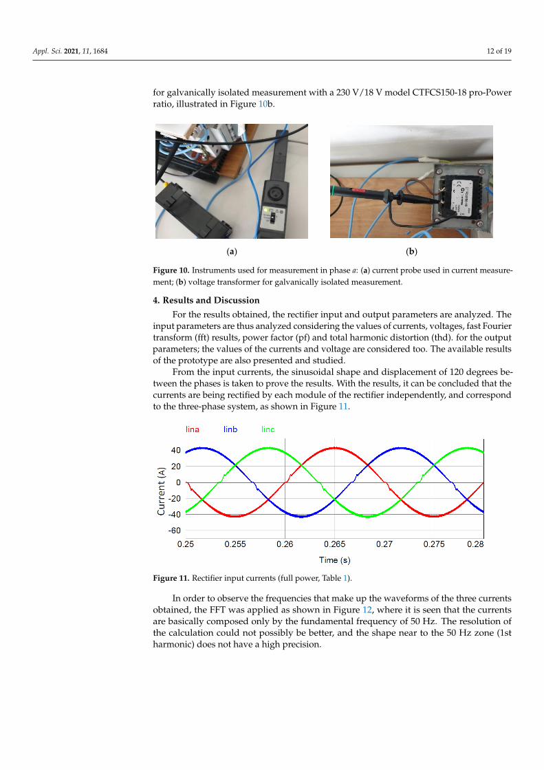
From the input currents, the sinusoidal shape and displacement of 120 degrees be-
tween the phases is taken to prove the results. With the results, it can be concluded that
the currents are being rectified by each module of the rectifier independently, and corre-
spond to the three-phase system, as shown in Figure 11.
Figure 11. Rectifier input currents (full power, Table 1).
Figure 10. Instruments used for measurement in phase a: (a) current probe used in current measure-ment; (b) voltage transformer for galvanically isolated measurement.
4. Results and Discussion
For the results obtained, the rectifier input and output parameters are analyzed. Theinput parameters are thus analyzed considering the values of currents, voltages, fast Fouriertransform (fft) results, power factor (pf) and total harmonic distortion (thd). for the outputparameters; the values of the currents and voltage are considered too. The available resultsof the prototype are also presented and studied.
From the input currents, the sinusoidal shape and displacement of 120 degrees be-tween the phases is taken to prove the results. With the results, it can be concluded that thecurrents are being rectified by each module of the rectifier independently, and correspondto the three-phase system, as shown in Figure 11.
Appl. Sci. 2021, 11, x FOR PEER REVIEW 12 of 20
Figure 9 illustrates some components of the interface circuit and control circuit that
are being tested due to the interconnection between them and their efficiencies. The com-
ponents are: (A) is drives (CGD15SG00D2) for the correct functioning of the IGBTs
(IXYN50N170CV1); (B) is the voltage hall sensor (LV 25-P); (C) is the precision rectifier;
(D) is the switch control; (E) are the current hall sensors (LAH 50-P); and (F) is the control
circuit 1 (UC3854B).
Some measured results from the reduced prototype tests are presented in Section 4,
together with the results by simulation.
Figure 10 illustrates the instruments used to measure current and voltage in phase a.
For current measurement, a current probe on the 10 mV/A scale shown in Figure 10a was
used. In the case of measuring the network voltage signal, a voltage transformer was used
for galvanically isolated measurement with a 230 V/18 V model CTFCS150-18 pro-Power
ratio, illustrated in Figure 10b.
(a) (b)
Figure 10. Instruments used for measurement in phase a: (a) current probe used in current meas-
urement; (b) voltage transformer for galvanically isolated measurement.
4. Results and Discussion
For the results obtained, the rectifier input and output parameters are analyzed. The
input parameters are thus analyzed considering the values of currents, voltages, fast Fou-
rier transform (fft) results, power factor (pf) and total harmonic distortion (thd). for the
output parameters; the values of the currents and voltage are considered too. The availa-
ble results of the prototype are also presented and studied.
From the input currents, the sinusoidal shape and displacement of 120 degrees be-
tween the phases is taken to prove the results. With the results, it can be concluded that
the currents are being rectified by each module of the rectifier independently, and corre-
spond to the three-phase system, as shown in Figure 11.
Figure 11. Rectifier input currents (full power, Table 1). Figure 11. Rectifier input currents (full power, Table 1).
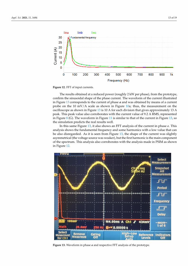
In order to observe the frequencies that make up the waveforms of the three currentsobtained, the FFT was applied as shown in Figure 12, where it is seen that the currentsare basically composed only by the fundamental frequency of 50 Hz. The resolution ofthe calculation could not possibly be better, and the shape near to the 50 Hz zone (1stharmonic) does not have a high precision.
Appl. Sci. 2021, 11, 1684 13 of 19
Appl. Sci. 2021, 11, x FOR PEER REVIEW 13 of 20
In order to observe the frequencies that make up the waveforms of the three currents
obtained, the FFT was applied as shown in Figure 12, where it is seen that the currents are
basically composed only by the fundamental frequency of 50 Hz. The resolution of the
calculation could not possibly be better, and the shape near to the 50 Hz zone (1st har-
monic) does not have a high precision.
Figure 12. FFT of input currents.
The results obtained at a reduced power (roughly 2 kW per phase), from the proto-
type, confirm the sinusoidal shape of the phase current. The waveform of the current il-
lustrated in Figure 13 corresponds to the current of phase a and was obtained by means
of a current probe on the 10 mV/A scale as shown in Figure 10a; thus, the measurement
on the oscilloscope as shown in Figure 13 is 10 A for each division that gives approxi-
mately 13 A peak. This peak value also corroborates with the current value of 9.2 A RMS,
represented in Figure 8 (G). The waveform in Figure 11 is similar to that of the current in
Figure 13, so the simulation predicts the real results well.
Figure 13. Waveform in phase a and respective FFT analysis of the prototype.
Figure 12. FFT of input currents.
The results obtained at a reduced power (roughly 2 kW per phase), from the prototype,confirm the sinusoidal shape of the phase current. The waveform of the current illustratedin Figure 13 corresponds to the current of phase a and was obtained by means of a currentprobe on the 10 mV/A scale as shown in Figure 10a; thus, the measurement on theoscilloscope as shown in Figure 13 is 10 A for each division that gives approximately 13 Apeak. This peak value also corroborates with the current value of 9.2 A RMS, representedin Figure 8 (G). The waveform in Figure 11 is similar to that of the current in Figure 13, sothe simulation predicts the real results well.
In this same Figure 13, it also shows an FFT analysis of the current in phase a. Thisanalysis shows the fundamental frequency and some harmonics with a low value that canbe also disregarded. As it is seen from Figure 13, the shape of the current was slightlyasymmetrical (the voltage source was weaker), but the first harmonic is the main componentof the spectrum. This analysis also corroborates with the analysis made in PSIM as shownin Figure 12.
Appl. Sci. 2021, 11, x FOR PEER REVIEW 13 of 20
In order to observe the frequencies that make up the waveforms of the three currents
obtained, the FFT was applied as shown in Figure 12, where it is seen that the currents are
basically composed only by the fundamental frequency of 50 Hz. The resolution of the
calculation could not possibly be better, and the shape near to the 50 Hz zone (1st har-
monic) does not have a high precision.
Figure 12. FFT of input currents.
The results obtained at a reduced power (roughly 2 kW per phase), from the proto-
type, confirm the sinusoidal shape of the phase current. The waveform of the current il-
lustrated in Figure 13 corresponds to the current of phase a and was obtained by means
of a current probe on the 10 mV/A scale as shown in Figure 10a; thus, the measurement
on the oscilloscope as shown in Figure 13 is 10 A for each division that gives approxi-
mately 13 A peak. This peak value also corroborates with the current value of 9.2 A RMS,
represented in Figure 8 (G). The waveform in Figure 11 is similar to that of the current in
Figure 13, so the simulation predicts the real results well.
Figure 13. Waveform in phase a and respective FFT analysis of the prototype. Figure 13. Waveform in phase a and respective FFT analysis of the prototype.

Appl. Sci. 2021, 11, 1684 14 of 19
The voltage and current in phase a for a 29 Ω load are shown in Figure 14, as anexample for the other phases (phase b, phase c). Note that the voltage and current aresinusoidal and are in phase, which resulted in high PF and low THD.
Appl. Sci. 2021, 11, x FOR PEER REVIEW 14 of 20
In this same Figure 13, it also shows an FFT analysis of the current in phase a. This
analysis shows the fundamental frequency and some harmonics with a low value that can
be also disregarded. As it is seen from Figure 13, the shape of the current was slightly
asymmetrical (the voltage source was weaker), but the first harmonic is the main compo-
nent of the spectrum. This analysis also corroborates with the analysis made in PSIM as
shown in Figure 12.
The voltage and current in phase a for a 29 Ω load are shown in Figure 14, as an
example for the other phases (phase b, phase c). Note that the voltage and current are
sinusoidal and are in phase, which resulted in high PF and low THD.
Figure 14. Voltage and currents in phase a, of the rectifier.
In order to evaluate the behavior of PF and THD more rigorously, several simulations
were carried out with different levels of load as described in Section 3, which allowed
obtaining Figure 15. In Figure 15a, it can be seen that the value of THD is inversely pro-
portional to load variation, that is, as the load value increases, THD decreases, thus ob-
taining a maximum THD of 4.98% for a load of 289 Ω (1%) and a minimum THD of 1.92%
in load 29 Ω (100%). The analysis of the PF illustrated in Figure 15b had the opposite be-
havior to THD. In this analysis, it is noted that the value of PF is directly proportional to
the variation of the load, that is, as the load increases, the PF increases, thus obtaining a
maximum PF of 99.98% for a load of 29 Ω (100%) and a minimum PF of 98.13% at a load
of 289 Ω (1%).
This shows that the proposed rectifier can operate at various load levels (below the
nominal load) and yet has the capacity to meet the recommendations of international
standards, IEEE 519 and IEC61000-3-2/IEC61000-3-4, with regard to the quality of electric-
ity. It is also found that the proposed rectifier is more efficient for fixed loads in which it
was designed.
(a) (b)
Figure 15. (a) THD for various load levels; (b) PF for various load levels.
Figure 14. Voltage and currents in phase a, of the rectifier.
In order to evaluate the behavior of PF and THD more rigorously, several simulationswere carried out with different levels of load as described in Section 3, which allowedobtaining Figure 15. In Figure 15a, it can be seen that the value of THD is inverselyproportional to load variation, that is, as the load value increases, THD decreases, thusobtaining a maximum THD of 4.98% for a load of 289 Ω (1%) and a minimum THD of1.92% in load 29 Ω (100%). The analysis of the PF illustrated in Figure 15b had the oppositebehavior to THD. In this analysis, it is noted that the value of PF is directly proportional tothe variation of the load, that is, as the load increases, the PF increases, thus obtaining amaximum PF of 99.98% for a load of 29 Ω (100%) and a minimum PF of 98.13% at a load of289 Ω (1%).
Appl. Sci. 2021, 11, x FOR PEER REVIEW 14 of 20
In this same Figure 13, it also shows an FFT analysis of the current in phase a. This
analysis shows the fundamental frequency and some harmonics with a low value that can
be also disregarded. As it is seen from Figure 13, the shape of the current was slightly
asymmetrical (the voltage source was weaker), but the first harmonic is the main compo-
nent of the spectrum. This analysis also corroborates with the analysis made in PSIM as
shown in Figure 12.
The voltage and current in phase a for a 29 Ω load are shown in Figure 14, as an
example for the other phases (phase b, phase c). Note that the voltage and current are
sinusoidal and are in phase, which resulted in high PF and low THD.
Figure 14. Voltage and currents in phase a, of the rectifier.
In order to evaluate the behavior of PF and THD more rigorously, several simulations
were carried out with different levels of load as described in Section 3, which allowed
obtaining Figure 15. In Figure 15a, it can be seen that the value of THD is inversely pro-
portional to load variation, that is, as the load value increases, THD decreases, thus ob-
taining a maximum THD of 4.98% for a load of 289 Ω (1%) and a minimum THD of 1.92%
in load 29 Ω (100%). The analysis of the PF illustrated in Figure 15b had the opposite be-
havior to THD. In this analysis, it is noted that the value of PF is directly proportional to
the variation of the load, that is, as the load increases, the PF increases, thus obtaining a
maximum PF of 99.98% for a load of 29 Ω (100%) and a minimum PF of 98.13% at a load
of 289 Ω (1%).
This shows that the proposed rectifier can operate at various load levels (below the
nominal load) and yet has the capacity to meet the recommendations of international
standards, IEEE 519 and IEC61000-3-2/IEC61000-3-4, with regard to the quality of electric-
ity. It is also found that the proposed rectifier is more efficient for fixed loads in which it
was designed.
(a) (b)
Figure 15. (a) THD for various load levels; (b) PF for various load levels. Figure 15. (a) THD for various load levels; (b) PF for various load levels.
This shows that the proposed rectifier can operate at various load levels (belowthe nominal load) and yet has the capacity to meet the recommendations of internationalstandards, IEEE 519 and IEC61000-3-2/IEC61000-3-4, with regard to the quality of electricity.It is also found that the proposed rectifier is more efficient for fixed loads in which itwas designed.
The voltage and current in phase a of the prototype is illustrated in Figure 16. Thevoltage form was obtained by means of a voltage transformer for galvanically isolatedmeasurement with a 230 V/18 V ratio, shown in Figure 10b; the current was obtained bymeans of a current probe on the 10 mV/A scale, shown in Figure 10a. This figure showsthat the current is in phase with the phase voltage, and therefore the PF value is 98% (by
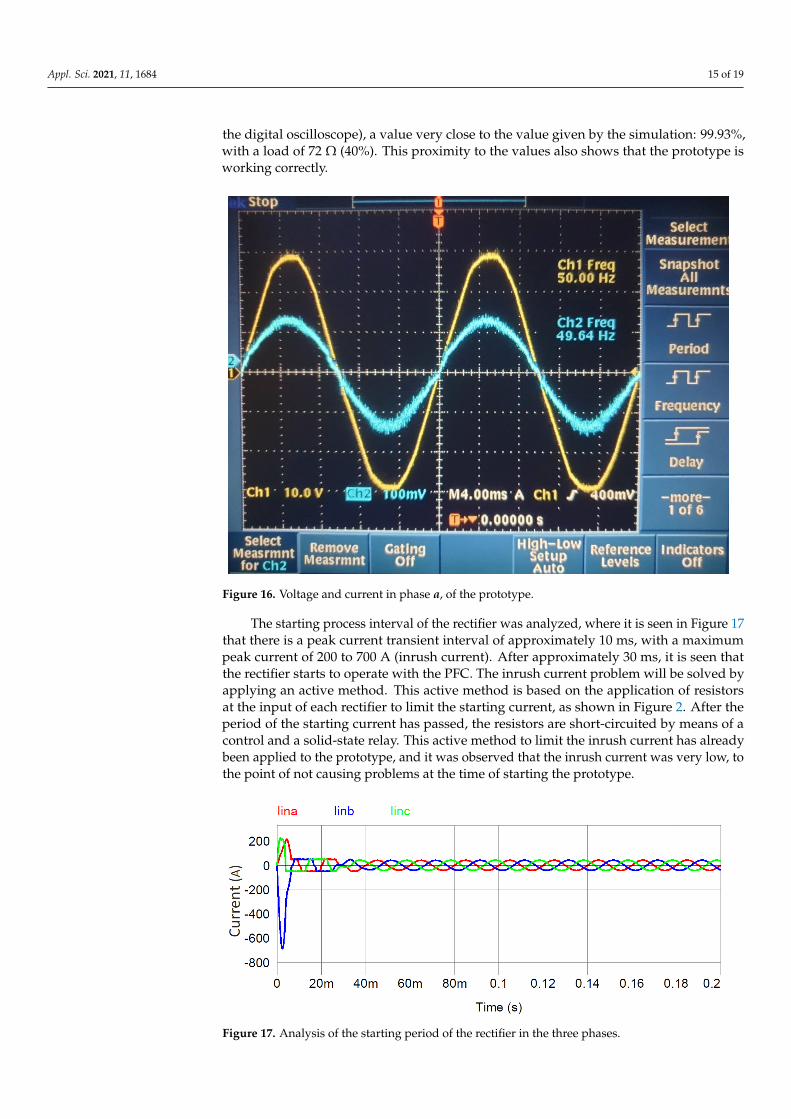
Appl. Sci. 2021, 11, 1684 15 of 19
the digital oscilloscope), a value very close to the value given by the simulation: 99.93%,with a load of 72 Ω (40%). This proximity to the values also shows that the prototype isworking correctly.
Appl. Sci. 2021, 11, x FOR PEER REVIEW 15 of 20
The voltage and current in phase a of the prototype is illustrated in Figure 16. The
voltage form was obtained by means of a voltage transformer for galvanically isolated
measurement with a 230 V/18 V ratio, shown in Figure 10b; the current was obtained by
means of a current probe on the 10 mV/A scale, shown in Figure 10a. This figure shows
that the current is in phase with the phase voltage, and therefore the PF value is 98% (by
the digital oscilloscope), a value very close to the value given by the simulation: 99.93%,
with a load of 72 Ω (40%). This proximity to the values also shows that the prototype is
working correctly.
Figure 16. voltage and current in phase a, of the prototype.
The starting process interval of the rectifier was analyzed, where it is seen in Figure
17 that there is a peak current transient interval of approximately 10 ms, with a maximum
peak current of 200 to 700 A (inrush current). After approximately 30 ms, it is seen that
the rectifier starts to operate with the PFC. The inrush current problem will be solved by
applying an active method. This active method is based on the application of resistors at
the input of each rectifier to limit the starting current, as shown in Figure 2. After the
period of the starting current has passed, the resistors are short-circuited by means of a
control and a solid-state relay. This active method to limit the inrush current has already
been applied to the prototype, and it was observed that the inrush current was very low,
to the point of not causing problems at the time of starting the prototype.
Figure 16. Voltage and current in phase a, of the prototype.
The starting process interval of the rectifier was analyzed, where it is seen in Figure 17that there is a peak current transient interval of approximately 10 ms, with a maximumpeak current of 200 to 700 A (inrush current). After approximately 30 ms, it is seen thatthe rectifier starts to operate with the PFC. The inrush current problem will be solved byapplying an active method. This active method is based on the application of resistorsat the input of each rectifier to limit the starting current, as shown in Figure 2. After theperiod of the starting current has passed, the resistors are short-circuited by means of acontrol and a solid-state relay. This active method to limit the inrush current has alreadybeen applied to the prototype, and it was observed that the inrush current was very low, tothe point of not causing problems at the time of starting the prototype.
Appl. Sci. 2021, 11, x FOR PEER REVIEW 16 of 20
Figure 17. Analysis of the starting period of the rectifier in the three phases.
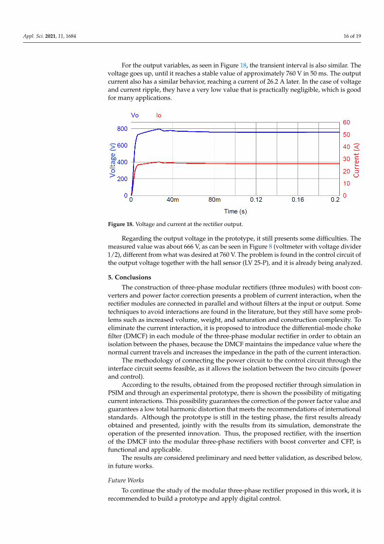
For the output variables, as seen in Figure 18, the transient interval is also similar.
The voltage goes up, until it reaches a stable value of approximately 760 V in 50 ms. The
output current also has a similar behavior, reaching a current of 26.2 A later. In the case
of voltage and current ripple, they have a very low value that is practically negligible,
which is good for many applications.
Figure 18. Voltage and current at the rectifier output.
Regarding the output voltage in the prototype, it still presents some difficulties. The
measured value was about 666 V, as can be seen in Figure 8 (voltmeter with voltage di-
vider 1/2), different from what was desired at 760 V. The problem is found in the control
circuit of the output voltage together with the hall sensor (LV 25-P), and it is already being
analyzed.
5. Conclusions
The construction of three-phase modular rectifiers (three modules) with boost con-
verters and power factor correction presents a problem of current interaction, when the
rectifier modules are connected in parallel and without filters at the input or output. Some
techniques to avoid interactions are found in the literature, but they still have some prob-
lems such as increased volume, weight, and saturation and construction complexity. To
eliminate the current interaction, it is proposed to introduce the differential-mode choke
filter (DMCF) in each module of the three-phase modular rectifier in order to obtain an
isolation between the phases, because the DMCF maintains the impedance value where
the normal current travels and increases the impedance in the path of the current interac-
tion.
Figure 17. Analysis of the starting period of the rectifier in the three phases.
Appl. Sci. 2021, 11, 1684 16 of 19
For the output variables, as seen in Figure 18, the transient interval is also similar. Thevoltage goes up, until it reaches a stable value of approximately 760 V in 50 ms. The outputcurrent also has a similar behavior, reaching a current of 26.2 A later. In the case of voltageand current ripple, they have a very low value that is practically negligible, which is goodfor many applications.
Appl. Sci. 2021, 11, x FOR PEER REVIEW 16 of 20
Figure 17. Analysis of the starting period of the rectifier in the three phases.
For the output variables, as seen in Figure 18, the transient interval is also similar.
The voltage goes up, until it reaches a stable value of approximately 760 V in 50 ms. The
output current also has a similar behavior, reaching a current of 26.2 A later. In the case
of voltage and current ripple, they have a very low value that is practically negligible,
which is good for many applications.
Figure 18. Voltage and current at the rectifier output.
Regarding the output voltage in the prototype, it still presents some difficulties. The
measured value was about 666 V, as can be seen in Figure 8 (voltmeter with voltage di-
vider 1/2), different from what was desired at 760 V. The problem is found in the control
circuit of the output voltage together with the hall sensor (LV 25-P), and it is already being
analyzed.
5. Conclusions
The construction of three-phase modular rectifiers (three modules) with boost con-
verters and power factor correction presents a problem of current interaction, when the
rectifier modules are connected in parallel and without filters at the input or output. Some
techniques to avoid interactions are found in the literature, but they still have some prob-
lems such as increased volume, weight, and saturation and construction complexity. To
eliminate the current interaction, it is proposed to introduce the differential-mode choke
filter (DMCF) in each module of the three-phase modular rectifier in order to obtain an
isolation between the phases, because the DMCF maintains the impedance value where
the normal current travels and increases the impedance in the path of the current interac-
tion.
Figure 18. Voltage and current at the rectifier output.
Regarding the output voltage in the prototype, it still presents some difficulties. Themeasured value was about 666 V, as can be seen in Figure 8 (voltmeter with voltage divider1/2), different from what was desired at 760 V. The problem is found in the control circuit ofthe output voltage together with the hall sensor (LV 25-P), and it is already being analyzed.
5. Conclusions
The construction of three-phase modular rectifiers (three modules) with boost con-verters and power factor correction presents a problem of current interaction, when therectifier modules are connected in parallel and without filters at the input or output. Sometechniques to avoid interactions are found in the literature, but they still have some prob-lems such as increased volume, weight, and saturation and construction complexity. Toeliminate the current interaction, it is proposed to introduce the differential-mode chokefilter (DMCF) in each module of the three-phase modular rectifier in order to obtain anisolation between the phases, because the DMCF maintains the impedance value where thenormal current travels and increases the impedance in the path of the current interaction.
The methodology of connecting the power circuit to the control circuit through theinterface circuit seems feasible, as it allows the isolation between the two circuits (powerand control).
According to the results, obtained from the proposed rectifier through simulation inPSIM and through an experimental prototype, there is shown the possibility of mitigatingcurrent interactions. This possibility guarantees the correction of the power factor value andguarantees a low total harmonic distortion that meets the recommendations of internationalstandards. Although the prototype is still in the testing phase, the first results alreadyobtained and presented, jointly with the results from its simulation, demonstrate theoperation of the presented innovation. Thus, the proposed rectifier, with the insertionof the DMCF into the modular three-phase rectifiers with boost converter and CFP, isfunctional and applicable.
The results are considered preliminary and need better validation, as described below,in future works.
Future Works
To continue the study of the modular three-phase rectifier proposed in this work, it isrecommended to build a prototype and apply digital control.

Appl. Sci. 2021, 11, 1684 17 of 19
Prototype: In this work, the results are considered preliminary, due to the simulationprocedure that was used for validation and the first results of the prototype test. To improvethe validation of the DMCF in a modular three-phase rectifier with boost converter, itis recommended to build 10 or 20 kW prototypes to be applied in wind systems or inaeronautics and spacecrafts.
Digital control: In this work, analog control was applied using the UC3854B integratedcircuit. This type of control has some technical disadvantages. Since digital electronics hasshown great gains in terms of application of control in converters, it is recommended toapply a digital control in the rectifier proposed. An example of integrated circuits withdigital control that can be applied is the XMC1402-Q040 × 0128 AA. In this way, the analogcontrol (UC3854B) can be compared with the digital control used.
Author Contributions: Creation and development of the proposed circuit: J.T.G.; analysis andvalidation of the proposed circuit and proofreading: S.V.; analysis, validation, and proofreading: R.M.The other parameters were made by the authors in a mutual way. All authors have read and agreedto the published version of the manuscript.
Funding: This research received no external funding.
Institutional Review Board Statement: Not applicable.
Informed Consent Statement: Not applicable.
Data Availability Statement: Not applicable.
Acknowledgments: Portuguese Foundation for Science and Technology and CTS, project UIDB/00066/2020;Foundation for Science and Technology (FCT) under the LAETA project UIDB/50022/2020; Founda-tion for Science and Technology (FCT) under the ICT (Institute of Earth Sciences) project UIDB/04683/2020.
Conflicts of Interest: The authors declare no conflict of interest.
Appendix AAppl. Sci. 2021, 11, x FOR PEER REVIEW 18 of 20
Figure A1. Power circuit.
Figure A2. Interface circuit.
Figure A1. Power circuit.
Appl. Sci. 2021, 11, 1684 18 of 19Appl. Sci. 2021, 11, x FOR PEER REVIEW 19 of 21
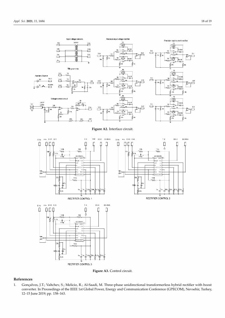
Figure A2. Interface circuit.
Figure A3. Control circuit.
References 1. Gonçalves, J.T.; Valtchev, S.; Melicio, R.; Al-Saadi, M. Three-phase unidirectional transformerless hybrid rectifier with boost
converter. In Proceedings of the IEEE 1st Global Power, Energy and Communication Conference (GPECOM), Nevsehir, Turkey, 12–15 June 2019; pp. 158–163.
Figure A2. Interface circuit.Appl. Sci. 2021, 11, x FOR PEER REVIEW 19 of 20
Figure A3. Control circuit.
References
1. Gonçalves, J.T.; Valtchev, S.; Melicio, R.; Al-Saadi, M. Three-phase unidirectional transformerless hybrid rectifier with boost
converter. In Proceedings of the IEEE 1st Global Power, Energy and Communication Conference (GPECOM), Nevsehir, Turkey,
12–15 June 2019; pp. 158–163.
2. Melicio, R.; Mendes, V.M.F.; Catalão, J.P.D.S. A pitch control malfunction analysis for wind turbines with permanent magnet
synchronous generator and full-power converters: proportional integral versus fractional-order controllers. Electr. Power Com-
pon. Syst. 2010, 38, 387–406.
3. Blaabjerg, F.; Liserre, M.; Ma, K. Power electronics converters for wind turbine systems. IEEE Trans. Ind. Appl. 2011, 48, 708–719.
4. Seixas, M., Melicio, R.; Mendes, V.M.F. Fifth harmonic and sag impact with a balancing new strategy for capacitor voltages.
Energy Convers. Manag. 2014, 79, 721–730.
5. Cavallo, A.; Guida, B.; Buonanno, A.; Sparaco, E. Smart buck-boost converter unit operations for aeronautical applications. In
Proceedings of the IEEE 54th Annual Conference on Decision and Control (CDC), Osaka, Japan, 15–18 December 2015; pp.
4734–4739.
6. Siebert, A.; Troedson, A.; Ebner, S. AC to DC power conversion now and in the future. IEEE Trans. Ind. Appl. 2002, 38, 934–940.
7. Kolar, J.W.; Friedli, T. The essence of three-phase PFC rectifier systems. In Proceedings of the 2011 IEEE 33rd International
Telecommunications Energy Conference (INTELEC), Amsterdam, The Netherlands, 9–13 October 2011; pp. 1–27.
8. Kolar, J.W.; Hartmann, M.; Friedli, T. Three-Phase PFC Rectifier and AC-AC Converter Systems-PART 1. In Proceedings of the
Tutorial at the Applied Power Electronics Conference and Exposition (APEC 2011), Fort Worth, TX, USA, 6–10 March 2011; pp.
6–10.
9. Sandeep, G.J.S.M.; Rasoolahemmed, S. Importance of active filters for improvement of power quality. IJETT. 2013, 4, 1164–1171.
10. Habibullin, M.; Pikalov, V.; Mescheryakov, V.; Valtchev, S. Active power filter with common dc link for compensation of har-
monic distortion in power grids. In Proceedings of the 2014 16th International Power Electronics and Motion Control Confer-
ence and Exposition, Antalya, Turkey, 21–24 September 2014, pp. 1345–1349.
Figure A3. Control circuit.
References1. Gonçalves, J.T.; Valtchev, S.; Melicio, R.; Al-Saadi, M. Three-phase unidirectional transformerless hybrid rectifier with boost
converter. In Proceedings of the IEEE 1st Global Power, Energy and Communication Conference (GPECOM), Nevsehir, Turkey,12–15 June 2019; pp. 158–163.

Appl. Sci. 2021, 11, 1684 19 of 19
2. Melicio, R.; Mendes, V.M.F.; Catalão, J.P.D.S. A pitch control malfunction analysis for wind turbines with permanent magnetsynchronous generator and full-power converters: Proportional integral versus fractional-order controllers. Electr. Power Compon.Syst. 2010, 38, 387–406. [CrossRef]
3. Blaabjerg, F.; Liserre, M.; Ma, K. Power electronics converters for wind turbine systems. IEEE Trans. Ind. Appl. 2011, 48, 708–719.[CrossRef]
4. Seixas, M.; Melicio, R.; Mendes, V.M.F. Fifth harmonic and sag impact with a balancing new strategy for capacitor voltages.Energy Convers. Manag. 2014, 79, 721–730. [CrossRef]
5. Cavallo, A.; Guida, B.; Buonanno, A.; Sparaco, E. Smart buck-boost converter unit operations for aeronautical applications.In Proceedings of the IEEE 54th Annual Conference on Decision and Control (CDC), Osaka, Japan, 15–18 December 2015;pp. 4734–4739.
6. Siebert, A.; Troedson, A.; Ebner, S. AC to DC power conversion now and in the future. IEEE Trans. Ind. Appl. 2002, 38, 934–940.[CrossRef]
7. Kolar, J.W.; Friedli, T. The essence of three-phase PFC rectifier systems. In Proceedings of the 2011 IEEE 33rd InternationalTelecommunications Energy Conference (INTELEC), Amsterdam, The Netherlands, 9–13 October 2011; pp. 1–27.
8. Kolar, J.W.; Hartmann, M.; Friedli, T. Three-Phase PFC Rectifier and AC-AC Converter Systems-PART 1. In Proceedings ofthe Tutorial at the Applied Power Electronics Conference and Exposition (APEC 2011), Fort Worth, TX, USA, 6–10 March 2011;pp. 6–10.
9. Sandeep, G.J.S.M.; Rasoolahemmed, S. Importance of active filters for improvement of power quality. IJETT 2013, 4, 1164–1171.10. Habibullin, M.; Pikalov, V.; Mescheryakov, V.; Valtchev, S. Active power filter with common dc link for compensation of harmonic
distortion in power grids. In Proceedings of the 2014 16th International Power Electronics and Motion Control Conference andExposition, Antalya, Turkey, 21–24 September 2014; pp. 1345–1349.
11. Antchev, M.H.; Petkova, M.P.; Antchev, H.M.; Gourgoulitsov, V.T.; Valtchev, S. Study of a single-phase series active power filterwith hysteresis control. In Proceedings of the 11th International Conference on Electrical Power Quality and Utilisation, Lisbon,Portugal, 17–19 October 2011; pp. 1–6.
12. de Freitas, L.G.; Simões, M.G.; Canesin, C.A.; de Freitas, L.C. Programmable PFC based hybrid multipulse power rectifier forultra clean power application. IEEE TPEL 2006, 21, 959–966. [CrossRef]
13. de Freitas, L.G.; Simoes, M.G.; Canesin, C.A.; de Freitas, L.C. A novel programmable PFC based hybrid rectifier for ultra cleanpower application. In Proceedings of the IEEE 35th Annual Power Electronics Specialists Conference, Aachen, Germany, 20–25June 2004; Volume 3, pp. 2172–2177.
14. Barbosa, P.M. Three-Phase Power Factor Correction Circuits for Low-Cost Distributed Power Systems. Ph.D. Theses, The BradleyDepartment of Electrical and Computer Engineering, Virginia Polytechnic Institute and State University, Blacksburg, VA, USA,2002.
15. de Freitas, L.G.; Coelho, E.A.; Simões, M.G.; Canesin, C.A.; de Freitas, L.C. Um novo retificador trifásico híbrido multipulsos comelevado fator de potência. Eletrônica Potência. 2005, 10, 17–24.
16. de Freitas, L.G.; Vincenzi, F.; Freitas, M.A.A.; Fernandes, E.R.; Mendonça, R.G.; de Freitas, L.C. Programmable PFC basedhybrid multipulse power rectifier with sinusoidal input line current imposed by digital controller. In Proceedings of the APEC07—Twenty-Second Annual IEEE Applied Power Electronics Conference and Exposition, Anaheim, CA, USA, 25 February–1March 2007; pp. 1356–1361.
17. Mao, H.; Lee, C.Y.; Boroyevich, D.; Hiti, S. Review of high-performance three-phase power-factor correction circuits. IEEE Trans.Ind. Electron. 1997, 44, 437–446.
18. Spiazzi, G.; Lee, F.C. Implementation of single-phase boost power-factor-correction circuits in three-phase applications. IEEETrans. Ind. Electron. 1997, 44, 365–371. [CrossRef]
19. Hahn, J.; Enjeti, P.N.; Pitel, I.J. A new three-phase power-factor correction (PFC) scheme using two single-phase PFC modules.IEEE Trans. Ind. Appl. 2002, 38, 123–130. [CrossRef]
20. Flores-Bahamonde, F.; Valderrama-Blavi, H.; Bosque, J.M.; Martínez-Salamero, L. Modular-based PFC for low power three-phasewind generator. In Proceedings of the 2011 7th International Conference-Workshop Compatibility and Power Electronics (CPE),Tallinn, Estonia, 1–3 June 2011; pp. 125–130.
21. Flores-Bahamonde, F.; Valderrama-Blavi, H.; Bosque-Moncusi, J.M.; Martinez-Salamero, L.; Leon-Masich, A.; Barrado, J.A.Single-Phase PFC for Three-Phase Wind Generator, a Modular Approach. System 2012, 7, 56–60.
22. Application Note, AN4511: Common Mode Filters, Life Augmented. Available online: https://www.st.com/content/ccc/resource/technical/document/application_note/d2/4d/6f/9d/bc/80/4d/97/DM00119609.pdf/files/DM00119609.pdf/jcr:content/translations/en.DM00119609.pdf (accessed on 3 October 2020).
23. Todd, P.C. UC3854 controlled power factor correction circuit design. UNITRODE Appl. Note 1999, U-134, 269–288.24. BARBI, I. Retificadores Monofásicos com Correção Ativa do Fator de Potência Empregando o Conversor Boost; Santa Catarina:UFSC:
Florianópolis, Brazil, 2015.