custom peripheral design guide - college of...
TRANSCRIPT

Custom Peripheral Design Guide
Introduction
This guide introduces you to the Create and Import Peripheral Wizard and guides you through thewhole process of creating a custom peripheral design in the Embedded Development Kit (EDK) andusing it in a processor system. The following are some of the Create and Import Peripheral Wizardfeatures: Create HDL templates for CoreConnect@ compliant custom peripheral design Deliver reference code of common features for peripheral implementation Provide EDK BFM simulation platform for peripheral verification Generate C driver template for software driver development Optionally generate ISE/XST projects for synthesis Create correct peripheral directory structure and user repository for importing custom peripherals
Objectives
After completing this guide, you will be able to: Understand the directory structure of EDK peripherals Generate custom peripheral design templates using Create and Import Peripheral Wizard Perform BFM simulation via EDK Write software driver of your own custom peripheral Build a processor system containing your custom peripheral to verify on board
Custom Peripheral Design Guide #1

Overview
This guide comprises 9 primary sections:
“Creating Hardware Processor System”“Creating Custom Peripheral Templates”“Implementing Custom Functionality”“Performing BFM simulation”“Importing to EDK”“Adding Custom Peripheral to System”“Implementing Software Driver”“Completing the User Application”“Downloading to Board”
For each step, you will find detailed instructions illustrated by screenshots. Feel free to skip certainsections based on your specific interest.
At the end of this guide, we also included an appendix to cover some topics and instructions on how todesign a mixed language peripheral using the templates (peripheral top-level template in VHDL andstub user-logic template in Verilog) generated by the wizard.
System Requirements
You must have the following software installed on your PC to complete this lab:
Windows 2000 SP2 or Windows XP EDK 7.1i or later ISE 7.1i or later ModelSim 5.7 or later
Hardware Requirements
In order to download the completed processor system, you must have the following hardware:
Xilinx Spartan-3 Starter Board – Revision E Xilinx Parallel Cable 4 used to program and debug the device Serial Cable
Note: It should be noted that other hardware could be used with this lab. However, the completeddesign has only been verified on the board specified above.
Custom Peripheral Design Guide #2

EDK Background
The Xilinx Embedded Development Kit (EDK) comes with a large number of commonly usedperipherals. Many different kinds of systems can be created with these peripherals, but it is likely thatyou may have to create your own custom peripheral to implement functionality not available in theEDK peripheral libraries and use it in your processor system.
To maximize the automation that EDK tools provide with you, when creating your own customperipheral you must take into account the following considerations:
The processor system by EDK is connected by OPB and/or PLB bus, so your custom peripheralmust be OPB or PLB compliant (see note). Meaning the top-level module of your customperipheral must contain a set of bus ports that is compliant to OPB or PLB protocol, so that it canbe attached to the system OPB or PLB bus. See figure 1-1.
Note: You may also create peripherals attached other bus interfaces that Xilinx supports as well,such as FSL bus interface. They are not covered in this guide.
To use your custom peripheral in EDK (s.t. XPS), your peripheral must be stored in a place(directory structure) that is accessible by various EDK tools; and you must have the correctPlatform Specification Format interface files (MPD and PAO files) to describe your customperipheral to EDK. See figure 1-2.
Custom Peripheral Design Guide #3
Figure 1-1: OPB bus protocol example
Figure 1-2: User peripheral directory structure

EDK uses Intellectual-Property Interface (IPIF) library to implement common functionality amongvarious processor peripherals. It is verified, optimized and highly parameterizeable. It also givesyou a set of simplified bus protocol called IP Interconnect (IPIC) which is much easier to userather than operate on OPB or PLB bus protocol directly. Using the IPIF module withparameterization that suits your needs will greatly reduce your design and test effort because youdon’t have to re-invent the wheel. See figure 1-3.
Figure 1-3: Using IPIF module in your peripheral
Considering all the above, you should use the following design flow when creating custom peripheralsin EDK:
Determine Interface: Identify the bus interface (s.t. OPB or PLB) your custom peripheralshould implement, so that it can be attached to that bus in your processor system.
Implement and Verify Functionality: Implement your custom functionality, reuse the commonfunctionality already available from EDK peripheral libraries as much as possible, and verify yourperipheral as a stand alone core.
Import to EDK: Copy your peripheral to an EDK recognizable directory structure and createthe PSF interface files (.mpd/.pao) so that other EDK tools can access your peripheral.
Add to System: Add your peripheral to the processor system in EDK.
Custom Peripheral Design Guide #4

Recommended Flow Using Wizard
The Create and Import Peripheral Wizard greatly simplify your custom peripheral creation process byguiding you through the design flow.
Here’re some of the benefits by using this tool:
Generate synthesisable VHDL/Verilog templates: this tool generates synthesisable HDLtemplates (for OPB/PLB peripherals, two HDL template files: peripheral top-level and user-logicHDL templates, where user-logic can be in either VHDL or Verilog for a mixed language design;for FSL peripherals, one HDL template file: peripheral top-level HDL template, in either VHDL orVerilog) for you to start your design; some code snippets may be provided as examples in HDLtemplate for your convenience.
Hide the complex OPB/PLB bus protocol: the templates generated by this tool takes care of allthe OPB/PLB bus interface protocol and connection between IPIF and your user logic, so you onlyneed to work on the much simplified IPIC protocol.
Configure IPIF module: this tool instantiates IPIF module in the peripheral top-level templateand parameterize different features (s.t. FIFO, Interrupt, DMA, etc.) to suit your needs, thus savesresources and development effort; leaves you to focus only on the custom functionality in userlogic itself.
Generate BFM simulation platform: optionally this tool can generate a BFM simulationplatform for your custom peripheral to help you verify your design using BFM simulation.
Generate implementation support files: optionally this tool can generate a number of auxiliaryfiles to save your time if you implement your peripheral in ISE and XST.
Generate software driver templates: optionally this tool can generate C driver templates for youto implement the software driver interface for your hardware peripheral, as well as a self testfunction to showcase the hardware features accessed via software.
Create directory structure: this tool will create the EDK compliant directory structure and PSFinterface files so various EDK tools can recognize your peripheral.
See figure 2-1.
Custom Peripheral Design Guide #5
Figure 2-1: Wizard generated directory structure and files
HDL Templates
Driver Templates
PSF interface files
BFM simulation project
Project Navigator project
XST synthesis project

So here’s the EDK custom peripheral creation flow we recommend:
Use Base System Builder (BSB) from XPS to generate a simple processor system that may useyour custom peripheral.
Use Create and Import Peripheral Wizard (create mode) to generate the HDL templates,BFM simulation platform, ISE support files and software driver templates, under the EDK projectyou created in step 1.
Use Project Navigator to open the .npl file generated in step 2, to implement your customfunctionality in user_logic.vhd file or add extra generics or user I/O to the peripheral top templatefile. Note: you can potentially edit the VHDL files in XPS without leaving the environment, but werecommend you to synthesis your individual peripheral first to make sure all your edits are eligible.
(Optional) perform BFM simulation in XPS to verify your design, using the BFM simulationplatform that the wizard created for you.
Use Create and Import Peripheral Wizard (import mode) to re-generate the EDK interfacefiles (.mpd/.pao) if necessary. Note: this step is only required if you added extra generics/ports instep 3 or created some other modules (files) in the design.
Use XPS - Add/Edit Core Dialog tool to add your custom peripheral to the processor systemyou created in step 1.
Use XPS or any other development tool to implement the software driver, if necessary, of yourcustom peripheral.
Use various EDK tools to compile, download and debug your processor system and peripheralon your development board.
Figure 2-2: Custom Peripheral Flow
Custom Peripheral Design Guide #6
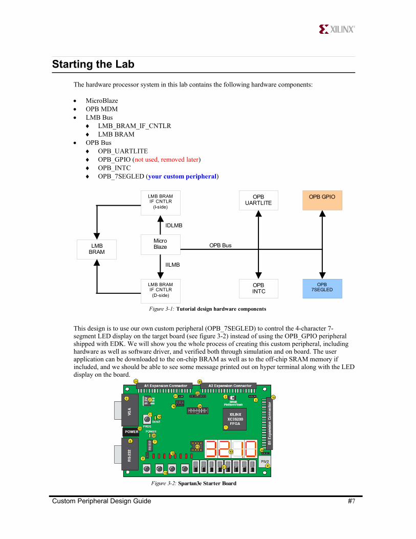
Starting the Lab
The hardware processor system in this lab contains the following hardware components:
MicroBlaze OPB MDM LMB Bus
LMB_BRAM_IF_CNTLR LMB BRAM
OPB Bus OPB_UARTLITE OPB_GPIO (not used, removed later) OPB_INTC OPB_7SEGLED (your custom peripheral)
This design is to use our own custom peripheral (OPB_7SEGLED) to control the 4-character 7-segment LED display on the target board (see figure 3-2) instead of using the OPB_GPIO peripheralshipped with EDK. We will show you the whole process of creating this custom peripheral, includinghardware as well as software driver, and verified both through simulation and on board. The userapplication can be downloaded to the on-chip BRAM as well as to the off-chip SRAM memory ifincluded, and we should be able to see some message printed out on hyper terminal along with the LEDdisplay on the board.
Figure 3-2: Spartan3e Starter Board
Custom Peripheral Design Guide #7
OPBUARTLITE
Figure 3-1: Tutorial design hardware components
MicroBlaze
LMB BRAMIF CNTLR(D-side)
LMB BRAMIF CNTLR
(I-side)
LMBBRAM
IILMB
IDLMB
OPB Bus
OPB GPIO
OPBINTC
OPB7SEGLED

Creating Hardware Processor System Step 1
This section covers using the Base System Builder (BSB) from Xilinx Platform Studio (XPS) to createthe hardware processor system that your custom peripheral will be attached to. Following are theprocedures you should perform to complete this step.
Open XPS, select Base System Builder Wizard from the popup Xilinx Platform Studio dialogand click OK to start BSB, see figure 4-1-1.
Figure 4-1-1: Xilinx Platform Studio dialog
Or from XPS main menu, select File New Project Base System Builder … to startBSB, see figure 4-1-2.
Figure 4-1-2: XPS menu
Custom Peripheral Design Guide #8

Specify a project path in the Create New Project Using Base System Builder Wizard dialogas shown in figure 4-2-1.
Enter Project File: C:\CreateIPLab Click OK
Figure 4-2-1: Create New Project Using Base System Builder Wizard dialog
It may take a while (1-2 minutes sometime) for Base System Builder wizard to load and getstarted. In the Base System Builder - Welcome screen (as shown in figure 4-2-2): Select I would like to create a new design Click Next
Custom Peripheral Design Guide #9
BSB is the easiest way to quickly create a hardware processor system onyour target board, it will also generate an example test program and linkerscript, as well as define PIN constraints on the UCF file.

In the Base System Builder – Select Board panel (as shown in figure 4-3): Select Board Vender: Xilinx Select Board Name: Spartan-3 Starter Board Select Board Revision: E Click Next
Figure 4-3: Base System Builder – Select Board
Custom Peripheral Design Guide #10
At any time, you may click the hyperlinks on the GUI for board informationor click on the More Info button for some quick help.
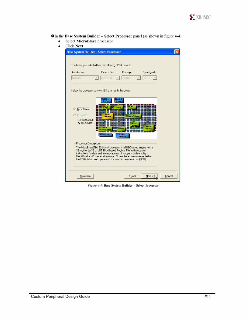
In the Base System Builder – Select Processor panel (as shown in figure 4-4): Select MicroBlaze processor Click Next
Figure 4-4: Base System Builder – Select Processor
Custom Peripheral Design Guide #11

In the Base System Builder – Configure Processor panel (as shown in figure 4-5): Accept all defaults of System Wide Settings and Processor Configuration Change Local Data and Instruction Memory to 16 KB Click Next
Figure 4-5: Base System Builder – Configure Processor
Custom Peripheral Design Guide #12
Since we selected a pre-defined board (in contrast to custom board), theFPGA device information on the board is fixed (grayed out on GUI). Alsonote, PowerPC is disabled since there’s no PowerPC processor onSpartan-3 devices.

In the Base System Builder – Configure IO Interfaces panel (as shown in figure 4-6): Select Use Interrupt for LED_7SEGMENT Deselect LEDs_8Bit from the IO Devices Click Next
Figure 4-6: Base System Builder – Configure IO Interfaces
Custom Peripheral Design Guide #13
Click on More Info button for some explanation of what the other choicesare about, or refer to Platform Studio User Guide for more detail.
You must make sure you have enough on-chip memory (BRAM) to storeyour program, the alternative is to store your program in off-chipmemory, s.t. SRAM. For this lab, we will allocate 16KB BRAM, whichshould be big enough for our application.
For your convenience, the target FPGA device (xc3s200) on our boardhas 221-Kb (27-KB) BRAM.
Please keep in mind that some peripherals may use BRAM resourcesas well.

In the Base System Builder – Configure Additional IO Interfaces panel (as shown in figure4-7):
Deselect Push_Buttons_3Bit from IO Devices Deselect DIP_Switches_8Bit from IO Devices Deselect SRAM_256Kx32 from IO Devices Click Next
Figure 4-7: Base System Builder – Configure Additional IO Interfaces
Custom Peripheral Design Guide #14
We will use the RS232 IO device (controlled by OPB UARTLITE) tocommunicate to the hyper terminal for our program standard in and out.
We will let BSB output correct PIN location for the 7 segment LEDdisplay to the auto generated UCF file by selecting theLED_7SEGMENT IO device (controlled by OPB GPIO, later we willreplace OPB GPIO with our own peripheral).
By selecting User Interrupt from any IO devices, BSB will automaticallyinclude an interrupt controller in the system to manage the interruptresources; later we will demonstrate interrupts from our own peripheral.

In the Base System Builder – Add Internal Peripherals panel (as shown in figure 4-8): Accept defaults and click Next
Figure 4-8: Base System Builder – Add Internal Peripherals
Custom Peripheral Design Guide #15

In the Base System Builder – Software Setup and Configure Memory Test Application panels(as shown in figure 4-9):
Accept all defaults in the Device to use as Standard Input and Standard Output,Sample Application Selection and Memory Test boxes
Click Next
Figure 4-9: Base System Builder – Software Setup and Configuration
Custom Peripheral Design Guide #16

Click on Generate and then Finish to complete the system generation, as shown in figure 4-10-1.
Figure 4-10-1: Base System Builder – System Created and Finished
Once the Base System Builder wizard is closed, you will go back to the Xilinx PlatformStudio IDE with the newly created CreateIPLab project opening up for you. Depending onyour setup, you may encounter the following popup (see figure 4-10-2) to inform platformstudio what you want to do next. Click OK to start using platform studio as the default (youmay want to check off the checkbox to stop this popup next time).
Figure 4-10-2: The Next StepTake some time to look at the hardware processor system (defined in system.mhs file) thatBSB created for you, as well as the UCF constraints (data/system.ucf file). See figure 4-10-3.
Custom Peripheral Design Guide #17
By accepting all the defaults in the software setup and configurationpanels, we will let BSB to generate a memory test application mainprogram (including link script) for us. Later, we will edit this main programto operate our custom peripheral via software driver.

Now you have a working system (the hardware processor system with a sample user application)that can be downloaded to board! The following steps are OPTIONAL and it may take sometime for the implementation tools to complete. To download the auto generated system to boardyou will need to:
Make sure your board is connected properly (connect the host computer to the targetboard, including connecting the Parallel 4 cable and the serial cable).
Start a HyperTerminal session with the following setting: com1 Bits per second: 9600 Data bits: 8 Parity: none Stop bits: 1 Flow control: none
Turn On the board power. Click Tools Download from XPS menu, this will cause the hardware/software system
to be built first and then iMPACT is used to configure the device. Once the device is configured, you should see the 4-character 7-segment LED display on
board flashing with different characters in sequence (Note: it is controlled by OPB GPIOat this time) and the HyperTerminal has similar print outs as shown in figure 4-11.
Figure 4-11: HyperTerminal output
After you are confirmed that the system generated by BSB is working and the LED display dowork on board, now we are ready to add our own customer peripheral to control the 7-segmentLED display. Go back to Xilinx Platform Studio (XPS) main window.
Custom Peripheral Design Guide #18

Creating Custom Peripheral Templates Step 2
In this step, we’ll create a user peripheral called opb_7segled to replace the opb_gpio peripheral(named LED_7SEGMENT) used in our hardware processor system generated above. This customized7-segment LED controller will be attached to the OPB bus and to control the 4-character 7-segmentLED display on our development board.
In XPS menu, select Tools Create/Import Peripheral… to start the wizard as shown infigure 5-1:
Click Next to continue
Figure 5-1: Create and Import Peripheral Wizard
Custom Peripheral Design Guide #19

In the flow panel (as shown in figure 5-2-1): Select Create templates for a new peripheral mode Click Next
Figure 5-2-1: Select create mode
Then in the Repository or Project panel (as shown in figure 5-2-2): Select add To an existing XPS project Select the XPS project you created before (C:\CreateIPLab\sysmte.xmp) from the drop
down list box Click Next
Custom Peripheral Design Guide #20
This wizard is able to create 4 types of CoreConnect compliantperipherals using the predefined IPIF libraries to reduce developmenteffort and time to market, it may also create FSL peripherals which is notcovered in this guide. The types of custom peripherals are:OPB slave-only peripheralOPB master-slave combo peripheralPLB slave-only peripheralPLB master-slave combo peripheralFSL master/slave peripheralClick on the hyperlinks to open up corresponding data sheets for detailinformation on what features are supported, or the More Info button forquick overview.

In the Name and Version panel (as shown in figure 5-3-1): Enter opb_7segled as peripheral top module name Accept the default version Click Next
Figure 5-3-1: Module name and revision
Then in the Bus Interfaces panel (as shown in figure 5-3-2): Select On-chip Peripheral Bus (OPB) that your custom peripheral will be attached to Click Next
Figure 5-3-2: Select bus interface
Custom Peripheral Design Guide #21
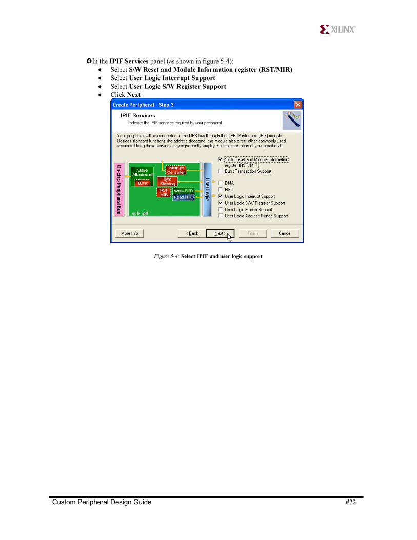
In the IPIF Services panel (as shown in figure 5-4): Select S/W Reset and Module Information register (RST/MIR) Select User Logic Interrupt Support Select User Logic S/W Register Support Click Next
Figure 5-4: Select IPIF and user logic support
Custom Peripheral Design Guide #22

In the Interrupt Service panel (as shown in figure 5-5): Deselect Use Device ISC Priority Encoder service Choose 1 as the Number of interrupts generated by user-logic Choose INTR_REG_EVENT as the Interrupt Capture Mode Click Next
Figure 5-5: Interrupt Service
Custom Peripheral Design Guide #23
The RST/MIR service is a module implemented in IPIF that allow yoursoftware program to individually reset your peripheral by writing a specialpattern to the RST register, and it also allow you to define a unique valuein the MIR register to identify your peripheral in the system.
User logic interrupt support will enable the interrupt controller modulewithin IPIF to hierarchically manage the interrupt resources either fromyour custom logic or from IPIF itself. Our custom peripheral will be ableto generate some interrupts for demonstration purpose.
We will also need to implement some software addressable registers tocontrol the 7-segment LED behavior, refer to Spartan-3 Starter KitBoard User Guide Chapter 3 for the 4-digit 7-segment LED displaydetail.

In the User S/W Register panel (as shown in figure 5-6), specify the number of softwareaddressable registers you want to implement in your user logic and their data width:
Choose 1 as the Number of software accessible registers (memory mapped) Accept the default 32 as the Data width of each register Click Next
Figure 5-6: User S/W Register
Custom Peripheral Design Guide #24
Please refer to corresponding IPIF data sheet for what the Device ISCPriority Encoder Service is about. For this design, we’re not going to usethis feature and by deselecting it to save some resource.
We will make our own custom peripheral to generate an interrupt everysecond. Later we will make our interrupt handler routine responding tothe interrupt and turn our controller into a 4-digit clock counter.
Click on the More Info button for a quick review of what theINTR_REG_EVENT capture mode is about.

In the IP Interconnect (IPIC) panel (as shown in figure 5-7): Accept the default IPIC signals wizard chooses for you based on your selections in
previous steps Click Next
Figure 5-7: IP Interconnect (IPIC)
Custom Peripheral Design Guide #25
Our custom peripheral controls the four 7-segment LEDs on the targetboard. We need four 8-bit registers to control the LED segments of eachcharacter (1 bit per segment including period), such that we can specifyexact hexadecimal characters (0 – 9, A, b, C, d, E, F) to be displayed. Wecould use four 8-bit registers, or combine all these 8-bit registers into one32-bit register. Here we use one 32-bit register to implement the four 8-bitregisters as required, and this allows IPIF to optimize away the bytesteering logic. Byte steering is not free, it could use as much as up toseveral hundred LUTs.

In the (OPTIONAL) Peripheral Simulation Support panel, there’s a hyperlink pointing you tothe BFM Toolkit Installation Instructions if you haven’t installed the BFM package on yourmachine as shown in figure 5-8-1. Check Generate BFM simulation platform to allow thewizard generate the BFM simulation test platform for your custom peripheral as shown in figure 5-8-2, and click Next to continue.
Figure 5-8-1: Peripheral Simulation Support
Custom Peripheral Design Guide #26
IPIC stands for IP Interconnect, it’s a simplified interface (protocol) thatallow you to hook up your custom function (user logic) to thecorresponding IPIF module and let IPIF worry about the master/slaveattachment and other common functionality, s.t. FIFO, DMA. Using IPIC,it’s possible that your custom function (user logic) can be easily attachedto either OPB or PLB bus, and you only need to take care of a small setof ports which is easy to understand and manage.
The wizard already selected all the IPIC ports that are necessary tocomplete the services/supports you choose in previous steps, typicallyyou don’t need to change anything here. But you’re free to add any extraIPIC ports that you want to use.
You must have installed the EDK BFM package onto your EDK installationin order to complete this step, otherwise a warning message will popup toforce you install the BFM package first.

In the (OPTIONAL) Peripheral Implementation Support panel (as shown in figure 5-9): Check Generate ISE and XST project files to help you implement the peripheral
using XST flow Check Generate template driver files to help you implement software interface Click Next
Figure 5-9: Peripheral Implementation Support
Custom Peripheral Design Guide #27
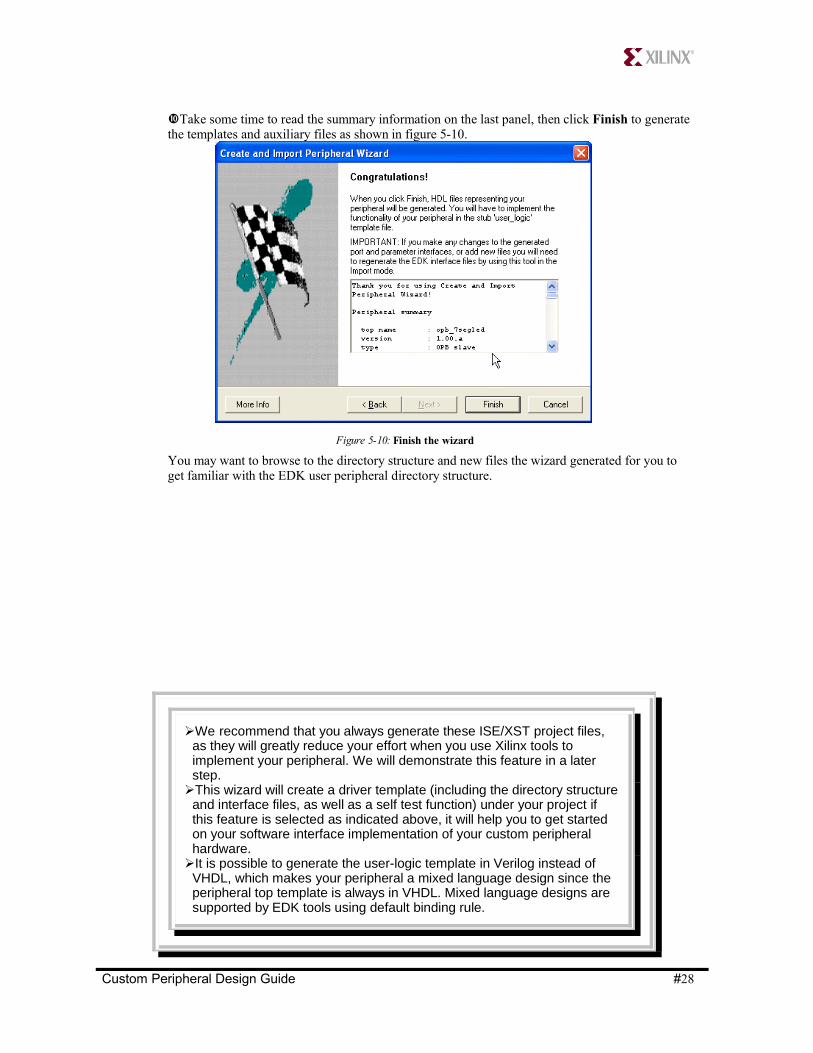
Take some time to read the summary information on the last panel, then click Finish to generatethe templates and auxiliary files as shown in figure 5-10.
Figure 5-10: Finish the wizard
You may want to browse to the directory structure and new files the wizard generated for you toget familiar with the EDK user peripheral directory structure.
Custom Peripheral Design Guide #28
We recommend that you always generate these ISE/XST project files,as they will greatly reduce your effort when you use Xilinx tools toimplement your peripheral. We will demonstrate this feature in a laterstep.
This wizard will create a driver template (including the directory structureand interface files, as well as a self test function) under your project ifthis feature is selected as indicated above, it will help you to get startedon your software interface implementation of your custom peripheralhardware.
It is possible to generate the user-logic template in Verilog instead ofVHDL, which makes your peripheral a mixed language design since theperipheral top template is always in VHDL. Mixed language designs aresupported by EDK tools using default binding rule.

Implementing Custom Functionality Step 3
The Spartan-3 Starter Kit board has a four-character, seven-segment LED display controlled by FPGAuser-I/O pins, as shown in figure 6-1. Each digit shares eight common control signals to light individualLED segments. Each individual character has a separate anode control input. To light an individualsignal, drive the individual segment control signal low along with the associated anode control signalfor the individual character.
Figure 6-1: Seven-Segment LED Digit Control
Therefore, our custom peripheral opb_7segled is designed to have 12 user I/O pins (8-bit segmentcontrol bus plus 4-bit anode control bus). One to control which digit to be set and the other to controlthe 8 LED segments (including the DP segment). We will implement one 32-bit register, to control all 4digits’ segment light status (8 bit per digit). See table below. Besides, we will also make our customperipheral to generate an interrupt every second.
Register Name AddressOffset fromPeripheral’sBase Address
AllowedAccess
Function
Display ControlRegister
+ 0x0 R/W Bit 0-7 : first digit (AN3)’s segmentsBit 8-15 : second digit (AN2)’s segmentsBit 16-23: third digit (AN1)’s segmentsBit 24-31: forth digit (AN0)’s segments
Custom Peripheral Design Guide #29
The auto-generated user peripheral VHDL templates come with all thecorrect PSF interface information that XPS needs to access, and thetemplates contain working example code snippets that the user couldmodify. So it can be attached to the hardware system in XPS directly atthis point as a dummy memory mapped peripheral
The custom peripheral’s HDL template is created under<your_XPS_project_dir>\pcores\opb_7segled_v1_00_a, below it a datadirectory stores the necessary PSF information for EDK tools torecognize this peripheral, a hdl directory stores the templates, and adevl directory stores all the help files for your simulation andimplementation.
The custom peripheral’s driver template is created under<your_XPS_project_dir>\drivers\opb_7segled_v1_00_a, below it a datadirectory stores the necessary PSF information for EDK tools torecognize this driver, and a src directory stores the driver template itself,as well as a self test function file.

We’ll use Project Navigator from ISE to implement our custom functionality, but you’re free to useother favorite tools to implement your design.
Here’s how to complete the custom functionality implementation of this step:
Custom Peripheral Design Guide #30

Start Project Navigator and open up the opb_7segled project by selecting the following ISEproject file: C:\CreateIPLab\pcores\opb_7segled_v1_00_a\devl\projnav\opb_7segled.npl
The ISE project file generated by the wizard is of pre-7.1 format (npl). ISE 7.1 or later willautomatically update the old format project file to its new format. Just click OK in the popupto let the tool take care of it. See figure 6-2-1.
Figure 6-2-1: ISE Update Project
Custom Peripheral Design Guide #31

Double click on the opb_7segled-imp item in the Module View tab to open up the peripheraltop-level template file opb_7segled.vhd as shown in figure 6-3-1.
Figure 6-3-1: opb_7segled.vhd
Add user port digit_n and segment_n below token --USER as shown in figure 6-3-2 below:
Custom Peripheral Design Guide #32
Depends on your environment, you may need to close the defaultproject opened by Project Navigator for you first; you may also possiblyget a complaint that your simulation environment is not setup properly,as shown in figure 6-2-2 below.
Figure 6-2-2: ISE Information
Sometime the update tool may popup fake warnings, as shown in figure6-2-3 below. Just ignore it.
Figure 6-2-3: ISE Information

Then search for token --USER again and add the user port mapping as shown in figure 6-3-3below. No other places need to be changed in this peripheral top-level template.
Figure 6-3-3: Map user port
New
Custom Peripheral Design Guide #33
COPY and PASTE
digit_n : out std_logic_vector(0 to 3);segment_n : out std_logic_vector(0 to 7);
New
Double click on the user_logic-imp item in the Module View tab to open up the user logictemplate file user_logic.vhd.
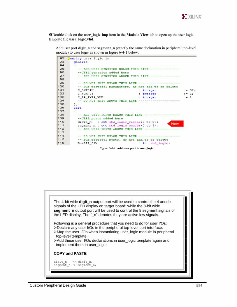
Add user port digit_n and segment_n (exactly the same declaration in peripheral top-levelmodule) to user logic as shown in figure 6-4-1 below.
Figure 6-4-1: Add user port to user_logic
New
Custom Peripheral Design Guide #34
The 4-bit wide digit_n output port will be used to control the 4 anodesignals of the LED display on target board; while the 8-bit widesegment_n output port will be used to control the 8 segment signals ofthe LED display. The “_n” denotes they are active low signals.
Following is a general procedure that you need to do for user I/Os:Declare any user I/Os in the peripheral top-level port interface.Map the user I/Os when instantiating user_logic module in peripheral
top-level template.Add these user I/Os declarations in user_logic template again and
implement them in user_logic.
COPY and PASTE
digit_n => digit_n,segment_n => segment_n,
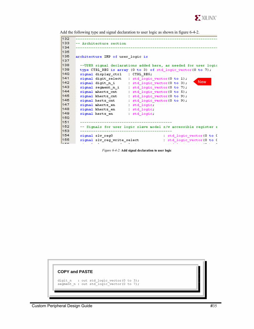
Add the following type and signal declaration to user logic as shown in figure 6-4-2.
Figure 6-4-2: Add signal declaration to user logic
New
Custom Peripheral Design Guide #35
COPY and PASTE
digit_n : out std_logic_vector(0 to 3);segment_n : out std_logic_vector(0 to 7);

Add your implementation code for custom functionality to control the LED display below theline “--USER logic implementation added here” as shown in figure 6-4-3 and 6-4-4.
Custom Peripheral Design Guide #36
According to the datasheet (see Spartan-3 Starter Kit Board UserGuide Chapter 3), the LED control signals are time-multiplexed to displaydata on all four characters. Through persistence of vision, the humanbrain perceives that all four characters appear simultaneously, similar tothe way the brain perceives a TV display. We’ll make our peripheralscanning at 1 kHz.
COPY and PASTE
type CTRL_REG is array (0 to 3) of std_logic_vector(0 to 7);signal display_ctrl : CTRL_REG;signal digit_select : std_logic_vector(0 to 1);signal digit_n_i : std_logic_vector(0 to 3);signal segment_n_i : std_logic_vector(0 to 7);signal mhertz_cnt : std_logic_vector(0 to 5);signal khertz_cnt : std_logic_vector(0 to 9);signal hertz_cnt : std_logic_vector(0 to 9);signal mhertz_en : std_logic;signal khertz_en : std_logic;signal hertz_en : std_logic;
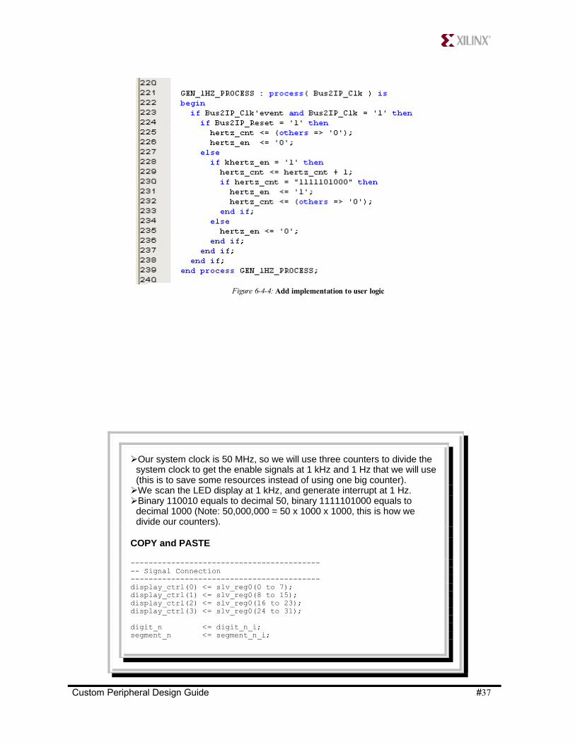
Figure 6-4-4: Add implementation to user logic
Custom Peripheral Design Guide #37
Our system clock is 50 MHz, so we will use three counters to divide thesystem clock to get the enable signals at 1 kHz and 1 Hz that we will use(this is to save some resources instead of using one big counter).
We scan the LED display at 1 kHz, and generate interrupt at 1 Hz.Binary 110010 equals to decimal 50, binary 1111101000 equals to
decimal 1000 (Note: 50,000,000 = 50 x 1000 x 1000, this is how wedivide our counters).
COPY and PASTE
-------------------------------------------- Signal Connection------------------------------------------display_ctrl(0) <= slv_reg0(0 to 7);display_ctrl(1) <= slv_reg0(8 to 15);display_ctrl(2) <= slv_reg0(16 to 23);display_ctrl(3) <= slv_reg0(24 to 31);digit_n <= digit_n_i;segment_n <= segment_n_i;

Continue add following scanning code below clock divider block as shown in figure 6-4-5.
Custom Peripheral Design Guide #38
COPY and PASTE
------------------------------------------ Clock Dividers----------------------------------------GEN_1MHZ_PROCESS : process( Bus2IP_Clk ) isbegin if Bus2IP_Clk'event and Bus2IP_Clk = '1' then if Bus2IP_Reset = '1' then mhertz_cnt <= (others => '0'); mhertz_en <= '0'; else mhertz_cnt <= mhertz_cnt + 1; if mhertz_cnt = "110010" then mhertz_en <= '1' ; mhertz_cnt <= (others => '0'); else mhertz_en <= '0'; end if; end if; end if;end process GEN_1MHZ_PROCESS;GEN_1KHZ_PROCESS : process( Bus2IP_Clk ) isbegin if Bus2IP_Clk'event and Bus2IP_Clk = '1' then if Bus2IP_Reset = '1' then khertz_cnt <= (others => '0'); khertz_en <= '0'; else if mhertz_en = '1' then khertz_cnt <= khertz_cnt + 1; if khertz_cnt = "1111101000" then khertz_en <= '1'; khertz_cnt <= (others => '0'); end if; else khertz_en <= '0'; end if; end if; end if;end process GEN_1KHZ_PROCESS;GEN_1HZ_PROCESS : process( Bus2IP_Clk ) isbegin if Bus2IP_Clk'event and Bus2IP_Clk = '1' then if Bus2IP_Reset = '1' then hertz_cnt <= (others => '0'); hertz_en <= '0'; else if khertz_en = '1' then hertz_cnt <= hertz_cnt + 1; if hertz_cnt = "1111101000" then hertz_en <= '1'; hertz_cnt <= (others => '0'); end if; else hertz_en <= '0'; end if; end if; end if;end process GEN_1HZ_PROCESS;

Search for the INTR_PROC process, comment it out (or simply remove it) and modify the codeas shown in figure 6-5-1 below.
Custom Peripheral Design Guide #39
COPY and PASTE
------------------------------------------ Display Update----------------------------------------CYC_DISP_PROCESS : process( Bus2IP_Clk ) isbegin if Bus2IP_Clk'event and Bus2IP_Clk = '1' then if Bus2IP_Reset = '1' then digit_select <= (others => '0'); digit_n_i <= (others => '1'); segment_n_i <= (others => '1'); else if khertz_en = '1' then digit_select <= digit_select + 1; case digit_select is when "00" => segment_n_i <= display_ctrl(0); digit_n_i <= "1110"; when "01" => segment_n_i <= display_ctrl(1); digit_n_i <= "1101"; when "10" => segment_n_i <= display_ctrl(2); digit_n_i <= "1011"; when "11" => segment_n_i <= display_ctrl(3); digit_n_i <= "0111"; when others => null; end case; end if; end if; end if;end process CYC_DISP_PROCESS;

Next, search for the SLAVE_REG_WRITE_PROC process and modify the default value forslv_reg0 to all ‘1’ when reset, as shown in figure 6-5-2 below.
Figure 6-5-2: Change slv_reg0 default when reset
Custom Peripheral Design Guide #40
COPY and PASTE
IP2Bus_IntrEvent(0) <= hertz_en;

Finally, save your changes and you are ready to synthesis your opb_7segled peripheral in ProjectNavigator. It’s not required to synthesis this design in Project Navigator, but we recommend youdo so to make sure there’s no typo and your changes are synthesizable (as shown in figure 6-6),you may also looking at circuit through View RTL Schematic.
Figure 6-6: Synthesize design
Close the project and Project Navigator, and go back to XPS window.
Custom Peripheral Design Guide #41
This is because the LED display’s segment control signals are active low,we should drive them to the inactive state when resetting.
COPY and PASTE
slv_reg0 <= (others => '1');

Performing BFM Simulation (Optional) Step 4
After you finish implementing the core, you can run BFM simulation to verify its functionality. BFM ismuch faster and easier to use than a manual testbench or system level simulation in XPS.
BFM stands for Bus Functional Model, it’s a toolkit developed by IBM and integrated into EDK tohelp user quickly perform behavioral simulation on the peripheral itself. The wizard is able to generatea BFM simulation test platform, which includes a simulation system including your peripheral, an IPtest bench which allow you to define user I/O stimulus, a sample BFL script synchronized with the IPtest bench to verify some basic features of your peripheral, as well as some other auxiliary files/scriptsto make the BFM simulation an easy task.
Figure 7-1 shows the BFM simulation system that the wizard generated for your opb_7segledperipheral (represented by the my IP block).
Figure 7-1: OPB Peripheral BFM System
For general instructions on how to continue BFM simulation based on the BFM simulation platformthat wizard generated for you, read the BFM Simulation Guide fromC:\CreateIPLab\pcores\opb_myled_cntlr_v1_00_a\devl\bfmsim\README.txt file. You may alsowant to explore the sub-directories and files under bfmsim before you continue this step.
The following procedure will guide you through the BFM simulation of the opb_7segled peripheral.
Custom Peripheral Design Guide #42

In XPS main window, close any project you already opened by clicking File Close Projectfrom the File menu. Then click File Open Project to open the BFM simulation project under
C:\CreateIPLab\pcores\opb_7segled_v1_00_a\devl\bfmsim\bfm_system.xmp as shown infigure 7-2-1.
Figure 7-2-1: open bfm_system.xmp project
If this is the first time you do simulation in EDK, please click on Options ProjectOptions… to open up the Project Options dialog. Click the HDL and Simulation tab andmake sure the Simulation Libraries Path – EDK Library and Xilinx Library – are filledout properly (they should point to the paths to which you compiled the simulation libraries onyour machine), example shown in figure 7-2-2 below.
Figure 7-2-2: Simulation Libraries Path
Custom Peripheral Design Guide #43

If you have not compiled the simulation libraries, click on the Compile button to start theEDK Simulation Library Compilation Wizard to compile the simulation libraries beforeyou continue, as shown in figure 7-2-3.
Note: compiling simulation libraries may take 20-30 minutes depending on your machine.
Figure 7-2-3: Compile Simulation Library Wizard
Custom Peripheral Design Guide #44

Click on File Open… from the XPS menu to open the IP test bench sourceC:\CreateIPLab\pcores\opb_7segled_v1_00_a\devl\bfmsim\pcores\opb_7segled_tb_v1_00_a\simhdl\vhdl\opb_7segled_tb.vhd file and do the following edits:
Add the anode_pin and segment_pin signals as shown in figure 7-3-1.
Figure 7-3-1: anode_pin and segment_pin signal declaration
New
Add the signal map as shown in figure 7-3-2.
Figure 7-3-2: signal map
New
Custom Peripheral Design Guide #45

Click on File Open… from the XPS menu to open the sample BFL command scriptC:\CreateIPLab\pcores\opb_7segled_v1_00_a\devl\bfmsim\scripts\sample.bfl file. Search forthe “Test User Logic S/W Register(s)” section and modify the data to be written toSLAVE_REG0 as shown in figure 7-4-1 below.
Figure 7-4-1: Modify sample.bfl
Custom Peripheral Design Guide #46
Because we’ve added user I/O (digit_n and segment_n) to theopb_7segled interface, we need to reflect the changes wheninstantiating the component in its IP test bench (opb_7segled_tb).
Do not modify the interface of opb_7segled_tb, as the IP test benchinterface is fixed for the BFM simulation platform.
You may also add any arbitrary VHDL code to this IP test bench file toperform other simulation testing the peripheral, s.t. verifying the userI/Os status, but be aware of the synchronous bus usage and follow theexample.
COPY and PASTE
signal anode_pin : std_logic_vector(0 to 3);signal segment_pin : std_logic_vector(0 to 7);
digit_n => anode_pin,segment_n => segment_pin,

Since the wizard has already generated a wave.do command script(C:\CreateIPLab\pcores\opb_7segled_v1_00_a\devl\bfmsim\scripts\wave.do) for us, wecan bring up any new user I/Os or other interested signals to the waveform window by editingthis wave.do file, or optionally we can add the signals later in the waveform window directly.For this lab, we will add the following lines to the wave.do file as shown in figure 7-4-2below.
Figure 7-4-2: Modify wave.do
Next, open the run.do(C:\CreateIPLab\pcores\opb_7segled_v1_00_a\devl\bfmsim\scripts\run.do) file that thewizard generated for to increase the simulation run time (to 10 ms instead of 100 us bydefault), as shown in figure 7-4-3.
Figure 7-4-3: Modify run.do
Custom Peripheral Design Guide #47
It doesn’t matter if you use other value for read/write here unless you putextra effort in the test bench file to convert the segment driver to displaycharacters.
COPY and PASTE
write(addr = SLAVE_REG0, be = SLAVE_REG0_BE, data = 0D249F03)read(addr = SLAVE_REG0, be = SLAVE_REG0_BE, data = 0D249F03)

Click on Tools Generate Simulation HDL files from the XPS menu as shown in figure 7-5-1. This will call the SimGen tool from EDK to compile the BFM simulation platform that thewizard generated for you.
Figure 7-5-1: Generate Simulation HDL files
It may take a while for SimGen to compile the BFM simulation model, after its completion,you should see the following message from XPS output console as shown in figure 7-5-2.
Custom Peripheral Design Guide #48
For more information on what BFL is about and how to use it, pleaserefer to <EDK_Install>/third_party/doc/OpbToolKit.pdf or PlbToolkit.pdf.
Pay attention to the duplicated my_core level when editing either thewave.do file or the sample.bfl file.
It may take you awhile to complete the 10 ms simulation.It should be noted that within 10 ms we wouldn’t see any interrupt
generated from our peripheral since we make it 1 interrupt per second.You can try simulating 1000 ms to verify the interrupt generation, but thiswill take you significant simulation time.
COPY and PASTE
add wave -noupdate -divider {LED Display PINs}add wave -noupdate -format Literal /bfm_system/my_core/my_core/anode_pinadd wave –noupdate –format Literal /bfm_system/my_core/my_core/segment_pin
run 10 ms

Click on the User Command 1 button, as shown in figure 7-6-1, to start BFM simulation.
Figure 7-6-1: User Command 1 button
It may take a while for ModelSim simulator to be launched, so do not click on the buttonmultiple times. Once ModelSim started, BFM simulation platform will be automaticallyloaded. The waveform can be viewed on the wave window after simulation completed asshown in figure 7-6-2.
Figure 7-6-2: ModelSim windows
Custom Peripheral Design Guide #49
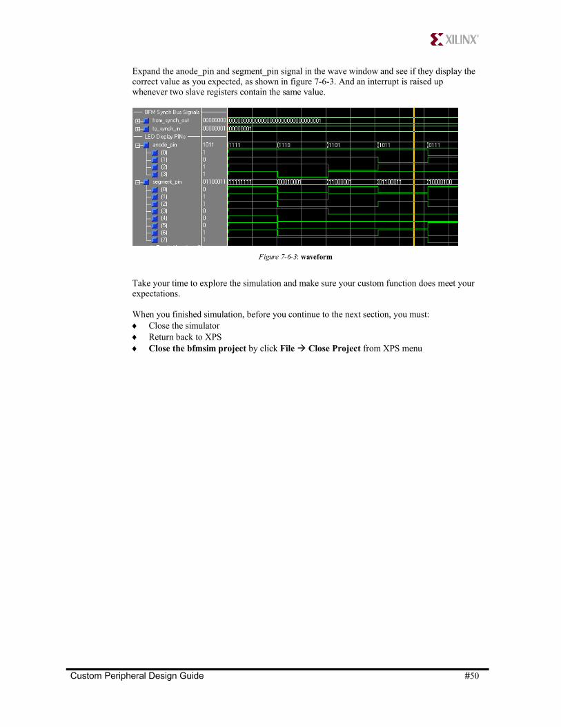
Expand the anode_pin and segment_pin signal in the wave window and see if they display thecorrect value as you expected, as shown in figure 7-6-3. And an interrupt is raised upwhenever two slave registers contain the same value.
Figure 7-6-3: waveform
Take your time to explore the simulation and make sure your custom function does meet yourexpectations.
When you finished simulation, before you continue to the next section, you must: Close the simulator Return back to XPS Close the bfmsim project by click File Close Project from XPS menu
Custom Peripheral Design Guide #50
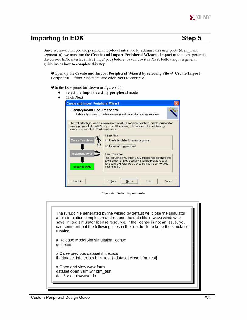
Importing to EDK Step 5
Since we have changed the peripheral top-level interface by adding extra user ports (digit_n andsegment_n), we must run the Create and Import Peripheral Wizard - import mode to re-generatethe correct EDK interface files (.mpd/.pao) before we can use it in XPS. Following is a generalguideline as how to complete this step.
Open up the Create and Import Peripheral Wizard by selecting File Create/ImportPeripheral… from XPS menu and click Next to continue.
In the flow panel (as shown in figure 8-1): Select the Import existing peripheral mode Click Next
Figure 8-1: Select import mode
Custom Peripheral Design Guide #51
The run.do file generated by the wizard by default will close the simulatorafter simulation completion and reopen the data file in wave window tosave limited simulator license resource. If the license is not an issue, youcan comment out the following lines in the run.do file to keep the simulatorrunning:
# Release ModelSim simulation licensequit -sim
# Close previous dataset if it existsif {[dataset info exists bfm_test]} {dataset close bfm_test}
# Open and view waveformdataset open vsim.wlf bfm_testdo ../../scripts/wave.do

In the Repository or Project panel (as shown in figure 8-2): Choose to import To an existing XPS project Select your current project from the drop down list (C:\CreateIPLab\system.xmp) Click Next
Figure 8-2: Add to existing XPS project
In the Core Name and Version panel (as shown in figure 8-3): Select opb_7segled from the drop down list box Check Use Version and accept 1.00.a Click Next
Figure 8-3: Enter name and version
Custom Peripheral Design Guide #52

In the Source File Types panel (as shown in figure 8-4): Check HDL Source Files(*.vhd, *.v) Click Next
Figure 8-4: Select HDL source files
In the HDL Source Files panel (as shown in figure 8-5): Select Use existing Peripheral Analysis Order file (*.pao) as the way to locate the HDL
source files Specify the PAO file generated in the create mode by using the Browse button:
C:\CreateIPLab\pcores\opb_7segled_v1_00_a\data\opb_7segled_v2_1_0.pao Click Next
Figure 8-5: Select .pao file
Custom Peripheral Design Guide #53

This HDL Analysis Information panel shows you all the dependent library files and HDLsource files to compile your peripheral, as well as corresponding logical libraries those files will becompiled into. You may click on Select Files or Select Libraries button in case you need to addmore files. For this custom peripheral, all files needed are automatically intuited by wizard basedon the PAO file. See figure 8-6. Click Next to continue.
Figure 8-6: List of all dependent library and source files
In the Bus Interfaces panel (as shown in figure 8-7): Check the OPB Slave (SOPB) bus interface Click Next
Figure 8-7: Select OPB Slave bus interface
Custom Peripheral Design Guide #54

Click Next until reach the SOPB: Parameter panel and verify that 256 Byte are selected as theMinimum size of address window as shown in figure 8-8. Click Next to continue.
Figure 8-8: SOPB: Parameter
Click Next until reach the last page and click Finish to close wizard as shown in figure 8-9.
Figure 8-9: Close wizard
Custom Peripheral Design Guide #55

You’ll see the dialog as shown in figure 8-10 to confirm completion of the Create and ImportPeripheral Wizard, just click OK.
Figure 8-10: Confirmation
Now your custom peripheral opb_7segled is ready to be used in XPS.
Custom Peripheral Design Guide #56
Adding Custom Peripheral to System Step 6
Now you’re ready to include the custom peripheral to the hardware processor system we generatedbefore. There’re several ways to do this. You can either edit the system.mhs file directly to add thecustom peripheral to the system and wire its digit and segment pins to control the 4-character 7-segment LED display on board, or you can achieve the same result by using the Add/Edit Core dialog.
In this section, we’ll guide you to use the Add/Edit Core dialog to use your custom peripheral.
Select File Open Project from the XPS menu to open the lab project(C:\CreateIPLab\system.xmp) we created before.
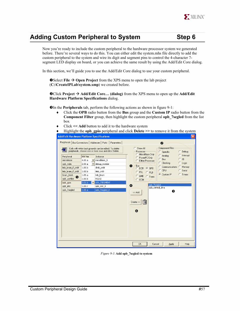
Click Project Add/Edit Core… (dialog) from the XPS menu to open up the Add/EditHardware Platform Specifications dialog.
In the Peripherals tab, perform the following actions as shown in figure 9-1: Click the OPB radio button from the Bus group and the Custom IP radio button from the
Component Filter group, then highlight the custom peripheral opb_7segled from the listbox
Click << Add button to add it to the hardware system Highlight the opb_gpio peripheral and click Delete >> to remove it from the system
Figure 9-1: Add opb_7segled to system
Custom Peripheral Design Guide #57

Switch to the Bus Connections tab, attach opb_myled_cntlr_0 to OPB bus as a salve device byclicking on the cell that corresponds to opb_7segled_0 sopb row and opb column, make surecharacter s appears on the cell, as shown in figure 9-2.
Figure 9-2: Attach to OPB as slave
Custom Peripheral Design Guide #58

Switch to the Addresses tab, click the Generate Addresses button to let XPS automaticallyassign addresses for all the peripherals for you, including the opb_7segled custom peripheral, asshown in figure 9-3.
Figure 9-3: Generate Addresses
Custom Peripheral Design Guide #59

Switch to the Ports tab, perform the following tasks as shown in figure 9-5: Select opb_7segled_0 from the Ports Filter combo box Highlight four ports (digit_n, segment_n, OPB_Clk and IP2INTC_Irpt) displayed
under opb_7segled_0 from the right list box Click << Add to add them to the Internal Ports Connections table Locate opb_7segled_0’s OPB_Clk port in the table, modify its Net Name to sys_clk_s
by selecting from its drop down list box Click the Add Port button to add two external ports: fpga_7SEGMENT_anode_pin and
fpga_7SEGMENT_segment_pin (connect to digit_out and segment_out respectively). Edit the Range column in the External Ports Connections table and make the above two
newly added external ports [0:3] and [0:7] respectively. Locate opb_7segled_0’s digit_n and segment_n port in the table, modify their Net
Name to digit_out and segment_out respectively by selecting from the combo box Highlight the fpga_0_LED_7SEGMENT_GPIO_d_out_pin port in the External Ports
Connections table and click Delete to remove it from the system interface
Figure 9-5: Modify port net name for opb_7segled_0
Custom Peripheral Design Guide #60

Still in the Ports tab, perform the following tasks as shown in figure 9-6. Search for the opb_intc_0 instance from the Internal Ports Connections table Click on the “…” button in the opb_intc_0’s Net Name cell to open up the Connect and
Prioritize Interrupts dialog Highlight the LED_7SEGMENT_IP2INTC_Irpt port and click the Remove >> button
to delete it from the interrupt controller’s priority list Highlight the opb_7segled_0_IP2INTC_Irpt port and click << Add button to add it to
the interrupt controller’s priority list Click OK to close the Connect and Prioritize Interrupts dialog
Figure 9-6: Modify interrupt priority
As a result, opb_intc_0’s Intr port should be connected to theopb_7segled_0_IP2INTC_Irpt port.
Custom Peripheral Design Guide #61

Click OK to close the Add/Edit Hardware Platform Specifications dialog, open up thesystem.mhs file and you should find similar opb_7segled section as shown in figure 9-7.
Figure 9-7: opb_7segled block in system.mhs
Custom Peripheral Design Guide #62

Open the UCF file that Base System Builder generated for you(C:\CreateIPLab\data\system.ucf) and do the following edits as shown in figure 9-8.
Figure 9-8: system.ucf
Custom Peripheral Design Guide #63
Implementing Software Driver Step 7
Software driver is a user-friendly interface between hardware component and software application,instead of operating on the memory mapped hardware component’s registers directly, you call certainuser-friendly driver functions in your software application to control and use the hardware component.It’s not required to write a software driver for every hardware component, especially those simplehardware like our opb_7segled custom peripheral, but it’s always a good approach to supply eachhardware component with a software driver thus to hide the hardware complexity from end user.
So far we’ve completed the hardware system specification including our custom peripheralopb_7segled, in this section we will show you how to implement a very simple software driver for ouropb_7segled custom peripheral.
You will notice that there’s a drivers directory (stores software drivers) created under our lab project(parallel to the pcores directory which stores hardware peripherals). A software driveropb_7segled_v1_00_a is already created below drivers by the wizard as we indicated in the Createand Import Peripheral wizard - create mode that we want the wizard to generate the software drivertemplate for us. This auto generated driver contains the correct directory structure and interface files(.mdd/.tcl) that make it recognizable by XPS, as well as the driver header/source template files.
Open the opb_7segled.h and opb_7segled.c files underC:\CreateIPLab\drivers\opb_7segled_v1_00_a\src directory and take a while to read the softwaredriver header/source template that the wizard generated. In the header file, some constants are definedfor your convenience to access applicable registers, two simple register peek/poke macros are defined,as well as some useful macros and a default interrupt handler declaration with its simpleimplementation in the corresponding source file. It’s totally up to you as how friendly you want thedriver to be.
You may also want to take a look at the self-test function that the wizard generated for you. It’s definedin the opb_7segled_selftest.c file. Depending on the features you selected in the wizard, this self-testfunction tries to access each individual feature of the hardware component sequentially, thus to verifythat the hardware component functioning properly.
As an example, we will define some simple driver functions in this section: a function to display 4digits on the LED display in a convenient way and re-implement the default interrupt handler given bywizard to make our custom peripheral functioning as a 4-digit clock counter.
Custom Peripheral Design Guide #64
COPY and PASTE
Net fpga_7SEGMENT_segment_pin<0> LOC=e14;Net fpga_7SEGMENT_segment_pin<1> LOC=g13;Net fpga_7SEGMENT_segment_pin<2> LOC=n15;Net fpga_7SEGMENT_segment_pin<3> LOC=p15;Net fpga_7SEGMENT_segment_pin<4> LOC=r16;Net fpga_7SEGMENT_segment_pin<5> LOC=f13;Net fpga_7SEGMENT_segment_pin<6> LOC=n16;Net fpga_7SEGMENT_segment_pin<7> LOC=p16;Net fpga_7SEGMENT_anode_pin<0> LOC=d14;Net fpga_7SEGMENT_anode_pin<1> LOC=g14;Net fpga_7SEGMENT_anode_pin<2> LOC=f14;Net fpga_7SEGMENT_anode_pin<3> LOC=e13;
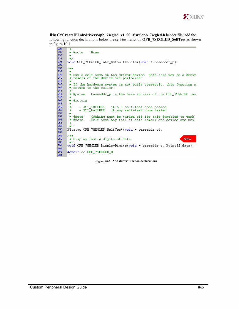
In C:\CreateIPLab\drivers\opb_7segled_v1_00_a\src\opb_7segled.h header file, add thefollowing function declarations below the self-test function OPB_7SEGLED_SelfTest as shownin figure 10-1.
Figure 10-1: Add driver function declarations
New
Custom Peripheral Design Guide #65

In C:\CreateIPLab\drivers\opb_7segled_v1_00_a\src\opb_7segled.c source file, add thefollowing function definitions at the bottom of the file as shown in figure 10-2.
Custom Peripheral Design Guide #66
COPY and PASTE
void OPB_7SEGLED_DisplayDigits(void * baseaddr_p, Xuint32 data);
COPY and PASTE
Xuint8 Digit[] ={ 0x03, // 0 0x9F, // 1 0x25, // 2 0x0D, // 3 0x99, // 4 0x49, // 5 0x41, // 6 0x1F, // 7 0x01, // 8 0x09 // 9};void OPB_7SEGLED_DisplayDigits(void * baseaddr_p, Xuint32 data){ Xuint32 baseaddr, val; Xuint8 i, dig; baseaddr = (Xuint32) baseaddr_p; val = data; for ( i = 0; i < 4; i++ ) { dig = Digit[val%10]; XIo_Out8(baseaddr+3-i, dig); val = val/10; }}

Search for the OPB_7SEGMENT_Intr_DefaultHandler function that the wizard defined for youand add a static count to make the LED display increase its displayed value every second, asshown in figure 10-3 below.
Figure 10-3: Re-implement interrupt handler
New
New
Custom Peripheral Design Guide #67

Save your changes and click on Tools Generate Libraries and BSPs from the XPS menu tomake sure your driver implementation is syntax correct. See figure 10-4.
Figure 10-4: Compile driver
Custom Peripheral Design Guide #68
The counter will rollover when reach 9999 since our LED display canonly display four digits.
Please comment out the xil_printf statement since calling printstatement in interrupt handler is very expensive.
COPY and PASTE
static Xuint32 count = 0;
if ( count < 9999 ) count++;else count = 0;OPB_7SEGLED_DisplayDigits(baseaddr_p, count);

Completing User Application Step 8
Now we need to work a little bit on the software application to use our custom 4-character 7-segmentLED Display controller through the software driver we just defined. Many thanks to the samplememory test application and linker script that Base System Builder wizard generated for us, the onlything left now is just to add a couple lines in the TestApp_Memory.c file.
Follow the procedure below:
In XPS main window, switch to the Applications tab and double click theC:\CreateIPLab\TestApp_Memory\src\TestApp_Memory.c file from the Project:TestApp_Memory – Sources to open the TestApp_Memory.c file as shown in figure 11-1.
Figure 11-1: Open TestApp_Memory.c
Custom Peripheral Design Guide #69

Comment out the gpio header file inclusion and include opb_7segled.h as well as othernecessary header files instead in TestApp_Memory.c as shown in figure 11-2. Also, remove theWriteToGPOutput function implementation.
Figure 11-2: Include header file
New
Custom Peripheral Design Guide #70

Still in the TestApp.c file, comment out the WriteToGPOutput function call and add line tocall opb_7segled’s self-test function instead as shown in figure 11-3. Then add code to startMicroBlaze interrupt so our interrupt handler can start working.
Figure 11-3: main application
New
Custom Peripheral Design Guide #71
COPY and PASTE
#include "xintc_l.h"#include "opb_7segled.h"

Save the changes and you may want to click Tools Build All User Applications to make sureyour edits are correct. See figure 11-4 below.
Figure 11-4: Compile application
Custom Peripheral Design Guide #72
COPY and PASTE
OPB_7SEGLED_SelfTest((void*) XPAR_OPB_7SEGLED_0_BASEADDR);// Start the interrupt controllerXIntc_mMasterEnable(XPAR_OPB_INTC_0_BASEADDR);// Enable opb_myled_cntlr's interruptOPB_7SEGLED_EnableInterrupt((void*) XPAR_OPB_7SEGLED_0_BASEADDR);// Enable adder interrupt in the interrupt controllerXIntc_mEnableIntr( XPAR_OPB_INTC_0_BASEADDR, XPAR_OPB_7SEGLED_0_IP2INTC_IRPT_MASK );// Enable MB interruptsmicroblaze_enable_interrupts();while ( 1 ) {}

Downloading to Board Step 9
This section requires the Xilinx Spartan-3 Starter board revision E (xc3s200) development board. Formore information on this board, refer to the Insight web site at http://www.insight-electronics.com/
Make sure your board is connected correctly (power, parallel 4 or JTAG, and serial cable). Start aHyperTerminal session (select 9600 bits per second and no flow control, refer to page 18 for detailinstructions) to capture the serial output from the development board.
Now click Tools Download from the XPS menu, the hardware system and software application wecompleted before will be built automatically and downloaded to the board. Note: this step may take10~20 minutes, please be patient.
After successful download, you should observe that all segments of the LED display on thedevelopment board turned on for awhile and then it reset to all zeros and starts increasing every second.There’re also some message printouts in the HyperTerminal. See figure 12-1.
Figure 12-1: HyperTerminal output
The hardware system uses our opb_7segled peripheral to control the 4-character 7-segment LEDDisplay on the starter board. Our opb_7segled peripheral has one software accessible register to controlthe 4 character’s display (8-bit per character). By setting this control register to different values throughthe interrupt handler, we make it functioning like a 4-digit clock counter. Remember that now the LEDdisplay is working under your own custom controller! Congratulations!
Custom Peripheral Design Guide #73

The following steps are OPTIONAL, to use XMD to debug the design. Please refer to EDKMicroBlaze tutorial for more detail instructions.
1. Make sure the device is configured and running.
2. Select Tools XMD.
3. If the first time to run XMD, XPS will require you to configure the XMD Debug Options inthe following dialog, just accept all defaults and save it.
Figure 10-1: Save XMD Debug Options
4. After XMD has initialized, it will automatically connect to the processor.
5. Now you can read and write opb_7segled’s register, as shown in figure 12-2 and watch forchanging of the 4-character 7-segment LED display. (Try 0D259F03 which will display 3210on the LED display)
Figure 12-2: Read/Write opb_7segled register
Custom Peripheral Design Guide #74
Verilog User Logic Appendix
Starting EDK 7.1i, the Create and Import Peripheral Wizard support mixed language designs. Meaningthe create flow can optionally generate a Verilog stub user-logic template instead of VHDL by default,while the peripheral top-level template still in VHDL in order to utilize the IPIF modules. And theimport flow can import peripherals implemented in both VHDL and Verilog languages. In this section,we will highlight some key steps to design such mixed language peripherals and show you the exampleto implement the above opb_7segled controller in a mixed language way.
You can follow the general procedures described in previous sections for your mixed language design,the only difference is that you’re now implement your custom logic using Verilog instead of VHDL.
Here are the instructions to complete your stub user-logic implementation in Verilog:
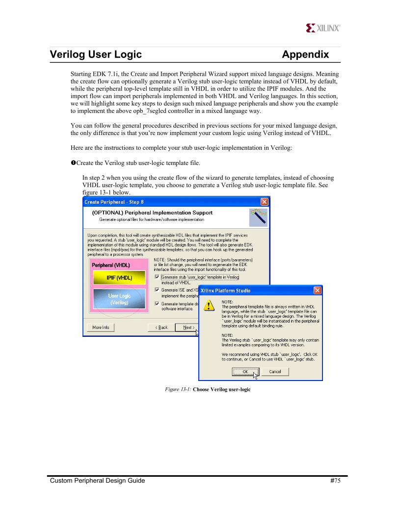
Create the Verilog stub user-logic template file.
In step 2 when you using the create flow of the wizard to generate templates, instead of choosingVHDL user-logic template, you choose to generate a Verilog stub user-logic template file. Seefigure 13-1 below.
Figure 13-1: Choose Verilog user-logic
Custom Peripheral Design Guide #75

Implement the custom logic in Verilog.
In Step 3, when you implement opb_7segled in Project Navigator, first open up the peripheral top-level template opb_7segled.vhd file and add the extra user I/Os in the user-logic componentdeclaration besides the two places (when declaring peripheral interface and when user-logic portmapping) we already did previously, as show in figure 13-2-1.
Figure 13-2-1: Add user I/O in component declaration
New
Custom Peripheral Design Guide #76
In the 7.1i, the Verilog stub user-logic will only give limited example codesfor the various features you selected in the wizard (only slave registerread/write examples are given at this time).

Still in Project Navigator, select the Library tab to open up the user_logic.v file as shown in figure13-2-2. This is because all verilog files will be compiled into the work library, it won’t show up inthe Module view tab.
Figure 13-2-2: Open user_logic.v
Add the two user I/O ports to the module interface as shown in figure 13-2-3.
Figure 13-2-3: Add user I/O
New
Custom Peripheral Design Guide #77
You should have noticed the difference here, instead of using directinstantiation of the stub user-logic module, we declare the stub Veriloguser-logic module as if it’s a regular VHDL component in the peripheraltop-level template file. XST will use default binding rule when synthesisyour mixed language designs. The port interface must match and allgenerics will be mapped to parameters in the Verilog module.
COPY and PASTE
digit_n : out std_logic_vector(0 to 3);segment_n : out std_logic_vector(0 to 7);

Declare their direction and dimension as shown in figure 13-2-4.
Figure 13-2-4: Declare port mode
New
Add the following signals as shown in figure 13-2-5.
Figure 13-2-5: Add signals
New
Custom Peripheral Design Guide #78
COPY and PASTE
digit_n,segment_n,

Add similar signal connection and clock divider code as you did in Step 3, shown in figure 13-2-6.
Custom Peripheral Design Guide #79
COPY and PASTE
output [0:3] digit_n;output [0:7] segment_n;
reg [0:3] digit_n;reg [0:7] segment_n; reg [0:1] digit_select;reg [0:5] mhertz_cnt;reg [0:9] khertz_cnt, hertz_cnt;wire mhertz_en, khertz_en, hertz_en;

Continue add similar scanning code as you did in Step 3 as shown in figure 13-2-7.
Finally, search for the SLAVE_REG_WRITE_PROC block and modify the default slave registervalue to all bit 1 since the LED display control signals are active low, as shown in figure 13-2-8.
Custom Peripheral Design Guide #80
COPY and PASTE
// ------------------------------------------------------// Signal Connection// ------------------------------------------------------assign mhertz_en = ( mhertz_cnt == 50 ) ? 1 : 0;assign khertz_en = ( mhertz_en == 1 && khertz_cnt == 1000 ) ? 1 : 0;assign hertz_en = ( khertz_en == 1 && hertz_cnt == 1000 ) ? 1 : 0;assign IP2Bus_IntrEvent[0] = hertz_en;// ------------------------------------------------------// Clock Divider// ------------------------------------------------------always @( posedge Bus2IP_Clk ) begin : GEN_1MHZ_PROCESS if ( Bus2IP_Reset == 1 ) mhertz_cnt = 0; else begin mhertz_cnt = mhertz_cnt + 1; if ( mhertz_cnt > 50 ) mhertz_cnt = 0; end end // GEN_1MHZ_PROCESSalways @( posedge Bus2IP_Clk ) begin : GEN_1KHZ_PROCESS if ( Bus2IP_Reset == 1 ) khertz_cnt = 0; else if ( mhertz_en == 1 ) begin khertz_cnt = khertz_cnt + 1; if ( khertz_cnt > 1000 ) khertz_cnt = 0; end end // GEN_1KHZ_PROCESSalways @( posedge Bus2IP_Clk ) begin : GEN_1HZ_PROCESS if ( Bus2IP_Reset == 1 ) hertz_cnt = 0; else if ( khertz_en == 1 ) begin hertz_cnt = hertz_cnt + 1; if ( hertz_cnt > 1000 ) hertz_cnt = 0; end end // GEN_1HZ_PROCESS

Import it back.
Since the peripheral interface has been changed, you need to use the wizard’s import flow to re-generate the PSF interface files. Now you’ll need to indicate that it’s a mixed language design, asshown in figure 13-3-1 and 13-3-2.
Custom Peripheral Design Guide #81
COPY and PASTE
// ------------------------------------------------------// -- Display Update// ------------------------------------------------------always @( posedge Bus2IP_Clk ) begin : CYC_DISP_PROCESS if ( Bus2IP_Reset == 1 ) digit_select = 0; else if ( khertz_en == 1 ) digit_select = digit_select + 1; end // CYC_DISP_PROCESSalways @( digit_select or slv_reg0 ) case ( digit_select ) 0 : begin segment_n <= slv_reg0[0:7]; digit_n <= 4'b1110; end 1 : begin segment_n <= slv_reg0[8:15]; digit_n <= 4'b1101; end 2 : begin segment_n <= slv_reg0[16:23]; digit_n <= 4'b1011; end 3 : begin segment_n <= slv_reg0[24:31]; digit_n <= 4'b0111; end default : ; endcase
slv_reg0 <= ~0;

Use your mixed language peripheral as usual.
Now you can verify and use your mixed language opb_7segled peripheral as usual in your BFM orhardware system.
Note: You may encounter some in-exist signals when doing BFM simulation using the wave.doscript generated by the wizard, if that’s the case, you can safely comment out those signals andthat’s because the Verilog user-logic template doesn’t contain example codes for all features at thistime.
Custom Peripheral Design Guide #82