data sheet ic-wt rev a0 · pdf filerev a0, page 2/13 description ... dpa, dna, dpb, dnb-1 1 ma...
TRANSCRIPT

iC-WTINCREMENTAL ENCODER
FEATURES APPLICATIONS
♦ Differential scanning for track A and B♦ Constant-light-evaluated scanning for the index track Z with
adjustable relative threshold♦ Photocurrent amplifier with high cut-off frequency♦ Current comparators with hysteresis♦ Index track Z selectable gated by tracks A and B♦ Current-limited and short-circuit-proof push-pull outputs♦ Outputs TTL compatible♦ Adjustable LED current control for constant optical receiver
power♦ Integrated 50mA driver for the transmit LED♦ LED current monitoring and error message upon violating
the control range♦ Low current consumption from single 5V power supply◊ Option: enhanced temperature range -40..125°C
♦ Photocurrent evaluation forincremental linear or angularposition measuring systems
PACKAGES
SO16N
BLOCK DIAGRAM
©1997 Rev A0
PHOTODIODES ARRAY
CO
DE
WH
EE
L
+5V
+5V
OUT_A
OUT_B
OUT_Z
ERROR
DRIVER
LED
LED CURRENT CONTROL
ERROR
TRACK A
TRACK B
TRACK Z
DPB
DPA
DZ
RLED68Ω
RLR15kΩ
DNB
DNA
CLR10nF 15kΩ
RZ
LED
16 AGND
3A
7LED
6NERR
4B
5Z
2
VCC
1
GND
11 DZ
14 DPA
15 DNA
12 DPB
13 DNB
8 CLR
10 ILR
9
iC-WT
IZ
iC-OR
iC-Haus GmbH Tel +49-6135-9292-0Integrated Circuits Fax +49-6135-9292-192Am Kuemmerling 18, D-55294 Bodenheim http://www.ichaus.com
iC-WTINCREMENTAL ENCODER
Rev A0, Page 2/13
DESCRIPTION
The device iC-WT is an evaluator IC for optical increment linear and rotary motion sensors, e.g. glassscales or shaft encoders.
A photodiodes array supplies the input signals for the monolithically integrated amplifiers, comparators andthe TTL compatible push-pull output drivers. Two tracks, A and B, are evaluated differentially, the indextrack Z as a constant light.
An integrated LED current control with driver stage enables the direct connection of a transmit LED withseries resistor and ensures a constant optical receive power. Two external resistors are used to set therelative index track comparator threshold and to determine the receive photocurrents.
The internally available logical AND operation of index track Z to tracks A and B can be switched off foradjustment.
A monitor circuit triggers an error message when the LED current control range is violated. The fault outputdesigned as an open collector is low active and simultaneously functions as an input to turn off the ANDoperation of the index track.
All connections are protected against damage due to ESD. The outputs are short-circuit proof.
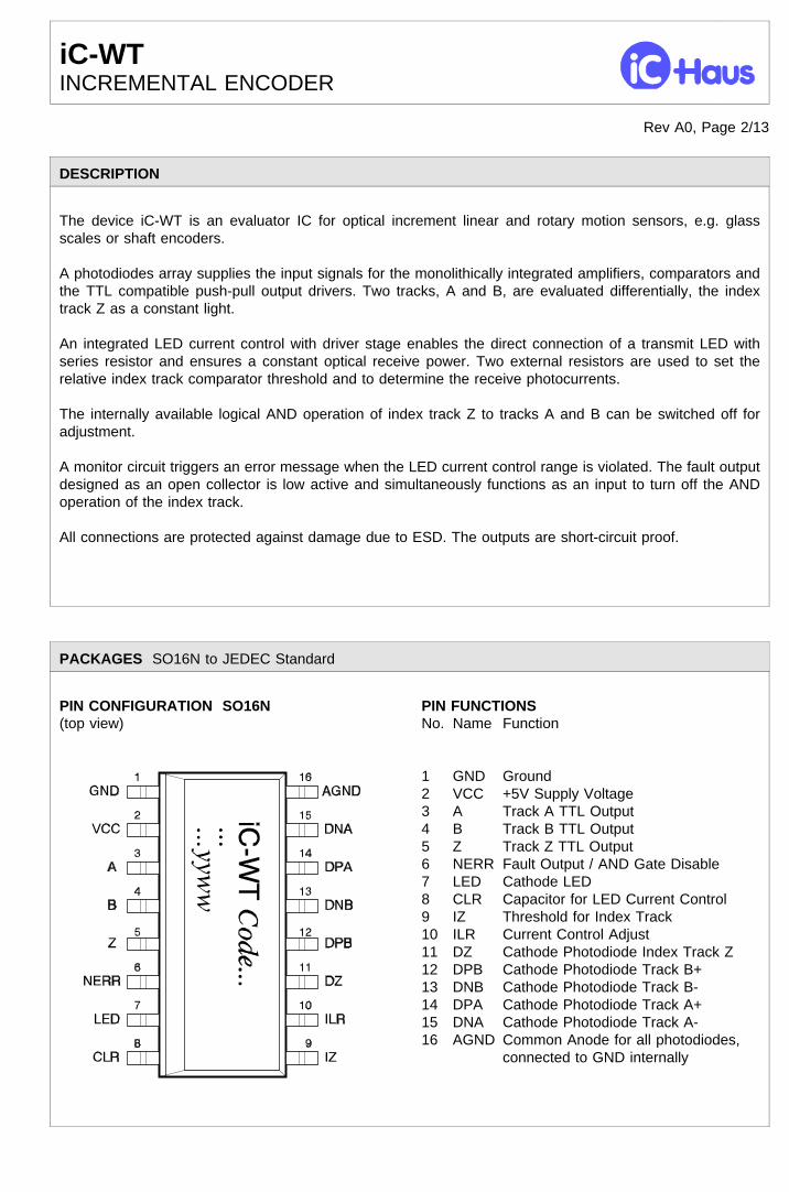
PACKAGES SO16N to JEDEC Standard
PIN CONFIGURATION SO16N PIN FUNCTIONS(top view) No. Name Function
1 GND Ground2 VCC +5V Supply Voltage3 A Track A TTL Output4 B Track B TTL Output5 Z Track Z TTL Output6 NERR Fault Output / AND Gate Disable7 LED Cathode LED8 CLR Capacitor for LED Current Control9 IZ Threshold for Index Track10 ILR Current Control Adjust11 DZ Cathode Photodiode Index Track Z12 DPB Cathode Photodiode Track B+13 DNB Cathode Photodiode Track B-14 DPA Cathode Photodiode Track A+15 DNA Cathode Photodiode Track A-16 AGND Common Anode for all photodiodes,
connected to GND internally

iC-WTINCREMENTAL ENCODER
Rev A0, Page 3/13
ABSOLUTE MAXIMUM RATINGS
Values beyond which damage may occur; device operation is not guaranteed.
Item Symbol Parameter Conditions Fig. Unit
Min. Max.
G001 VCC Supply Voltage 0 7 V
G002 I(DPx)I(DNx)
Current in InputsDPA, DNA, DPB, DNB
-1 1 mA
G003 V(A,B,Z) Voltage at Outputs A, B, Z 0 VCC
G004 I(A,B,Z) Current in Outputs A, B, Z V(A,B,Z)< 0V or V(A,B,Z)> VCC -4 4 mA
G005 I(DZ) Current in Input DZ -1 1 mA
G006 I(ILR)I(IZ)
Current in ILR, IZ -6 1 mA
G007 I(CLR) Current in CLR -1 1 mA
G008 I(LED) Current in LED V(LED)> VCC -1 1 mA
G009 I(LED) Current in LED V(LED)≤ VCC -1 60 mA
G010 V(NERR) Voltage at NERR 0 VCC
G011 I(NERR) Current in NERR V(NERR)< 0 or V(NERR)> VCC -4 4 mA
TG1 Tj Junction Temperature -30 130 °C
TG2 Ts Storage Temperature -30 130 °C
THERMAL DATA
Operating Conditions: VCC= 5V ±10%
Item Symbol Parameter Conditions Fig. Unit
Min. Typ. Max.
T1 Ta Operating Ambient TemperatureRange(extended temperature range onrequest)
-25 125 °C
T2 Rthja Thermal ResistanceChip to Ambient
SMD mounting, without specialcooling
125 K/W
All voltages are referenced to ground unless otherwise noted.All currents into the device pins are positive; all currents out of the device pins are negative.

iC-WTINCREMENTAL ENCODER
Rev A0, Page 4/13
ELECTRICAL CHARACTERISTICS
Operating Conditions: VCC= 5V ±10%, Tj= -25..125°C, unless otherwise noted
Item Symbol Parameter Conditions Tj Fig. Unit
°C Min. Typ. Max.
Total Device
001 VCC Permissible Supply Voltage 4.5 5.5 V
002 I(VCC) Supply Current in VCC,Outputs A, B, Z hi
closed LED control:R(ILR/AGND)= 15kΩ,I(LED)≈ 3mA, NERR= hi;I(A,B,Z)= 0, R(RZ/AGND)= 15kΩ,I(DZ,DPx)= -400nA,I(DNx)= -40..0nA, (x= A,B)
10 mA
003 I(VCC) Supply Current in VCC,Outputs A, B, Z lo
closed LED control:R(ILR/AGND)= 15kΩ,I(LED)≈ 3mA, NERR= hi;I(A,B,Z)= 0, R(RZ/AGND)= 15kΩ,I(DZ,DPx)= -40..0nAI(DNx)= -400nA
27 5.512 mA
mA
004 fo Cut-off Frequencyfor Tracks A and B
sinusoidal waveform,I(DPx)= -20..-400nA,I(DNx)= -400..-20nA
500 kHz
005 fo Cut-off Frequencyfor Index Track Z
rectangular waveform,I(DZ)= -20..-400nA,threshold 200nA
250 kHz
006 ∆tp() Propagation Delay Deviationtrack vs.track at A, B, Z
100 ns
Differential Photocurrent Amplifier, Track A and B
101 I(DPx)I(DNx)
Permissible Sensor Current atDPA, DNA, DPB, DNB
-600 0 nA
102 CM(P/N) Common Mode DPA vs. DNA,DPB vs. DNB
0.85 1 1.15
Comparator, Track A and B
201 Hys Hysteresis refered to [I(DPx) +I(DNx)] / 2
I(DPx,DNx)= -400..0nA 15 20 25 %
Photocurrent Amplifier, Index Track Z
401 I(DZ) Permissible Sensor Current at DZ -600 0 nA
Comparator, Index Track Z
801 Hys Hysteresis refered to I(DZ) I(DZ)= -400..0nA 7 10 13 %
Push-Pull Outputs A, B, Z
301 Vs()hi Saturation Voltage hi Vs()hi= VB-V();I()= -400µA
-252770
125
0.90.8
0.750.7
1.11.00.90.9
VVVV
302 Vs()hi Saturation Voltage hi Vs()hi= VB-V();I()= -1.6mA
-252770
125
1.21.1
1.051.05
1.51.41.31.3
VVVV
303 Vs()lo Saturation Voltage lo I()= 0.8mA 0.4 V
304 Vs()lo Saturation Voltage lo I()= 1.6mA 0.5 V
305 Isc()hi Short-Circuit Current hi V()= 0V..2.8V27
-8-3.5
-1.7 mAmA

iC-WTINCREMENTAL ENCODER
Rev A0, Page 5/13
ELECTRICAL CHARACTERISTICS
Operating Conditions: VCC= 5V ±10%, Tj= -25..125°C, unless otherwise noted
Item Symbol Parameter Conditions Tj Fig. Unit
°C Min. Typ. Max.
Push-Pull Outputs A, B, Z (continued)
306 Isc()lo Short-Circuit Current lo V()= 1V..VCC27
26
13 mAmA
307 Vc()hi Clamp Voltage hi Vc()hi= V()-VCC; I()= 4mA 0.4 1.5 V
308 Vc()lo Clamp Voltage lo I()=-4mA -1.5 -0.4 V
LED Current Control, pins CLR, ILR, IZ, LED
601 ISUM Permissible Total Sensor Currentat DPA, DNA, DPB, DNB
ISUM= I(DPA)+I(DNA) +I(DPB)+I(DNB);
-1500 -50 nA
602 I(LED) Permissible Driver Current in LED 0.1 50 mA
603 Vs(LED) Saturation Voltage lo at LED I(LED)= 50mA,I(ILR)> 5µA, ISUM= 0 27
0.40.8
1.2 VV
604 V(ILR)V(IZ)
Voltage at ILR, IZ I(ILR,IZ)= -150..-5µA 1.15 1.22 1.28 V
606 Isc(ILR)Isc(IZ)
Short-Circuit Current in ILR, IZ V(ILR)= 0, V(IZ)= 027
-5-2.4
mAmA
607 CR(ILR) Current Ratio I(ILR)/ISUM closed LED control,ISUM= -800..-50nA
80 100 125
608 CR(IZ) Current Ratio I(IZ)/I(DZ) closed LED control,I(DZ)= -400..-10nA
320 400 500
609 Vc()hi Clamp Voltage hiat LED, CLR, ILR, IZ
VCC= 0V, I()= 1mA 0.4 1.0 V
610 Vc()lo Clamp Voltage loat LED, CLR, ILR, IZ
VCC= 0V, I()=-1mA -1.0 -0.4 V
Error Detection, AND Gate Select, Input/Output NERR
501 R(NERR) Internal Pull-Up Resistor 20 30 45 kΩ
502 Vt()Gate AND Gate Turn-Off Threshold Gate disabled if V(NERR)< 0.4V27
0.40.5
1 VV
701 Vs()lo Saturation Voltage lo I(NERR)= 1.6mA27 0.15
0.4 VV
702 Vs()lo Saturation Voltage lo I(NERR)= 5mA27 0.25
0.8 VV
703 Isc()lo Short-Circuit Current lo V(NERR)= 2V..VCC27
515
30 mAmA
704 Vc()hi Clamp Voltage hi Vc()hi= V(NERR)-VCC;NERR=hi, I(NERR)= 4mA
0.4 1.5 V
705 Vc()lo Clamp Voltage lo NERR=lo, I(NERR)=-4mA -1.5 -0.4 V
iC-WTINCREMENTAL ENCODER
Rev A0, Page 6/13
APPLICATIONS INFORMATION
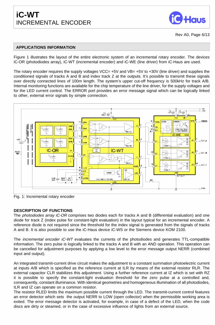
Figure 1 illustrates the layout of the entire electronic system of an incremental rotary encoder. The devicesiC-OR (photodiodes array), iC-WT (incremental encoder) and iC-WE (line driver) from iC-Haus are used.
The rotary encoder requires the supply voltages VCC= +5V and VB= +5V to +30V (line driver) and supplies theconditioned signals of tracks A and B and index track Z at the outputs. It’s possible to transmit these signalsover directly connected lines of 100m length. The system’s upper cut-off frequency is 500kHz for track A/B.Internal monitoring functions are available for the chip temperature of the line driver, for the supply voltages andfor the LED current control. The ERROR port provides an error message signal which can be logically linkedto other, external error signals by simple connection.
Fig. 1: Incremental rotary encoder
DESCRIPTION OF FUNCTIONSThe photodiodes array iC-OR comprises two diodes each for tracks A and B (differential evaluation) and onediode for track Z (index pulse for constant-light evaluation) in the layout typical for an incremental encoder. Areference diode is not required since the threshold for the index signal is generated from the signals of tracksA and B. It is also possible to use the iC-Haus device iC-WS or the Siemens device KOM 2100.
The incremental encoder iC-WT evaluates the currents of the photodiodes and generates TTL-compatibleinformation. The zero pulse is logically linked to the tracks A and B with an AND operation. This operation canbe cancelled for adjustment purposes by applying a low level to the error message output NERR (combinedinput and output).
An integrated transmit-current drive circuit makes the adjustment to a constant summation photoelectric currentat inputs A/B which is specified as the reference current at ILR by means of the external resistor RLR. Theexternal capacitor CLR stabilizes this adjustment. Using a further reference current at IZ which is set with RZit is possible to specify the constant-light evaluation threshold for the zero pulse at a controlled and,consequently, constant illuminance. With identical geometries and homogeneous illumination of all photodiodes,ILR and IZ can operate on a common resistor.The resistor RLED limits the maximum possible current through the LED. The transmit-current control featuresan error detector which sets the output NERR to LOW (open collector) when the permissible working area isexited. The error message detector is activated, for example, in case of a defect of the LED, when the codediscs are dirty or steamed, or in the case of excessive influence of lights from an external source.
iC-WTINCREMENTAL ENCODER
Rev A0, Page 7/13
The line driver iC-WE possesses short-circuit-proof push-pull output stages for the tracks A, B and Z. Thedrivers typically supply 300mA at VB= 24V and are internally adapted for a characteristic impedance of 75Ω.The outputs can be inverted via input INV (active-high). Consequently, when two line drivers are used, abalanced activation of the line is also possible. Tri-state switching of the output stages is possible to support bussystems (input TRI). An error detector monitors the chip temperature as well as the supply voltages VCC andVB. In the event of a fault, the open-collector output NER is switched low and the output stages are switchedto high impedance to prevent destruction. The error signal of the incremental encoder iC-WT can be switchedthrough to the output NER via the error input TNER.
DIMENSIONINGAdjusting the LED current controlSince the photodiodes DPA to DNA and DPB to DNB have anti-phase illumination, the following applies for thecontrol parameter ISUM as a function of the photocurrent peak value Iph,max. of a photodiode:
ISUM I(DPA) I(DNA) I(DPB) I(DNB) 2 ×Iph,max
Multiplied by the current transmission factor of the LED current control CR(ILR), the current to be set at ILR is(see electrical characteristics, No.607):
IILR ISUM ×CR(ILR) 2 ×Iph,max ×CR(ILR)
This current can be set with a resistor RLR connected to AGND. Due to the reference voltage V(ILR) beingapplied to pin ILR, this produces:
RLRV(ILR)I(ILR)
V(ILR)2 ×Iph,max ×CR(ILR)
Example: As a setpoint, the photodiodes should be illuminated so brightly that it conducts a photocurrent Iph,max=400nA at a maximum. With the electrical characteristics No.604 for V(ILR) and No.607 for CR(ILR) the resultis:
RLR1.22
2 ×400nA ×10015.25kΩ
Adjusting the index track comparator thresholdThe comparator threshold for the index signal is defined via a further reference current. The photocurrent Iph,max
is also obtained as the maximum for the photodiode DZ in the event of homogeneous illumination and samephotodiodes for track A/B and track Z. The maximum signal-to-noise ratio is attained with the constant-lightevaluation threshold:
Ith
Iph,max
2
Analogue to the calculation of RLR, it follows that:
IIZ Ith × CR(IZ)
RZV(IZ)I(IZ)
V(IZ)Ith ×CR(IZ)
Example: As a setpoint, the threshold Ith should be 200nA. With the electrical characteristics No.604 for V(IZ)and No.608 for CR(IZ) the result is:
RZ1.22V
200nA ×40015.25kΩ
iC-WTINCREMENTAL ENCODER
Rev A0, Page 8/13
If the current from ILR is the same as the current from IZ, a common resistor with the value RLR,Z= RLR / 2 = RZ
/ 2 can be utilized (in the example, 15.25 kΩ / 2 = 7.625 kΩ). ILR is connected directly to IZ.
Limiting the current for the transmit LEDThe resistance RLED limits the maximum current through the LED. It is calculated with the minimum forwardvoltage Vfw,min of the LED used for illumination, the minimum saturation voltage of the LED pin Vs(LED)(electrical characteristics No.603) and the permissible transmit current for the driver output I(LED)max (electricalcharacteristics No.602):
RLED
VCCmax Vfw,min Vs(LED)min
I(LED)max
Example: RLED= (5.5V - 1.2V - 0.4V) / 50mA = 78Ω
The lowest value for the current limiting is obtained by inserting the maximum saturation voltage of the LED pinVs(LED)max and the maximum LED forward voltage Vfw,max:
I(LED)lim≥VCCmin Vfw,max Vs(LED)max
RLED
Example: I(LED)lim= (4.5V - 1.5V - 1.2) / 78Ω ≈ 19mAThe limiting value inserted for the saturation voltage Vs(LED)max of 1.2V is not achieved by currents under50mA. The real minimum value for current limiting is therefore a little higher.
Capacitor at CLRThe value of capacitor CLR is not critical. The bottom of the permissible value range is restricted by the stabilityof control. The following applies:
CLR,min1nF × 15kΩ
RLR
Upwardly, the value is limited by the dead time τ of the LED current control after switching on the supplyvoltage:
CLR,max0.25 × τ
RLR
Example: τ= 100ms, RLR= 15kΩ: CLR,max= (0.25 × 100ms) / 15kΩ ≈ 1.5µF
PRINTED CIRCUIT BOARD LAYOUT
The following aspects should be noted when creating the PCB layout:
- Short connections between photodiodes array and iC-WT to minimize couplings and interference on thesmall photocurrents.
- Short-circuit the anodes of the photodiodes to pin AGND of the iC-WT. The connection to GND is madeexclusively inside the chip.
- Switch RLR, RZ, CLR to AGND too.- Do not run the printed conductors of the outputs of iC-WT and iC-WE in the vicinity of the connections
between photodiodes array and iC-WT or decouple by means of a GND conductor between them.- Connecting point of a metal reticle for the photodiodes array is GND on the iC-WT.

iC-WTINCREMENTAL ENCODER
Rev A0, Page 9/13
DEMO BOARD
The demonstration board provides a survey over the properties of the iC-WT simply and easily. The encoderIC is already connected to the necessary external components. In addition, the board contains subunits whichcan be utilized to have measurements performed - even without a rotary encoder. Figures 2 to 4 show thewiring as well as the top and bottom layout of the test PCB.
Fig. 2: Schematic diagram of the Demo Board
Fig. 3: Demo Board (components side) Fig. 4: Demo Board (solder dip side)

iC-WTINCREMENTAL ENCODER
Rev A0, Page 10/13
MEASUREMENTS WITH THE DEMO BOARD
The iC-WT can be examined at three different levels:
1. Static wiring of the sensor inputs with constant currents (using DIP switches)2. Dynamic wiring of the sensor inputs using function generator and current mirror circuit3. Dynamic wiring of the sensor inputs using a rotary encoder with photodiodes array
A regulated power supply of +5V dc must be applied between VCC and GND for all measurements. Since theiC-WT operates with very low sensor currents, the work surface should possess an insulated screen (e.g. asingle sided copper-clad plate) which is connected to GND. AGND is pulled down to GND inside the iC-WT andshould not be interconnected externally. The transmit LED of the rotary encoder can be connected betweenLED and VCC. For the visual check in case of measurements without rotary encoder a colored LED isrecommended.
1.1 Static function of A, B and ZShut off the AND operation of index signal Z with A and B by connecting the combined input/output NERR toground; the red control LED will light up. The two trimming potentiometers should be in the middle positioninitially, the DIP switches opened.
Closing a DIP switch of No.4 to No.8 connects the corresponding sensor input to AGND via a resistor (R4 toR8). Since each input is at constant (but temperature-dependent!) voltage potential V(T), a constant currentresults of the magnitude:
I= V(T) / R.
The result at room temperature is about:I= 1.8V / 4.3MΩ = 420nA
This current is supposed to simulate the photocurrent of an illuminated photodiode. An open switch simulatesa diode which is not illuminated (I= 0).The tracks A and B are evaluated differentially. The corresponding output is high (low) when current is onlyflowing from the P(ositive) (N(egative)) input. If the two inputs are conducting no current or the same current,the output remains in its old state due to hysteresis.Track Z is compared to a current threshold set using the trimmer RZ. If the input current is higher, the outputZ is high. The current flowing from IZ is specified with RZ:
IIZ= V(IZ) / RZ
The current threshold set is obtained with the aid of the current transmission factor CR(IZ) as:Ith= V(IZ) / (CR(IZ) × RZ)
When the trimmer is at the middle setting, the following applies:Ith= 1.22V / (400 × 12.5kΩ) = 244nA
The resistance value set with RZ can be measured after removing the jumper JZ.
1.2 LED current control and error outputThe function of the current control can be checked with an LED connected between LED and VCC. The voltageat NERR is displayed by the red LED on the demo board. It lights up when NERR is active, i.e. low.The setpoint of the receive power is set at pin ILR by using trimmer RLR. The resistance value can bemeasured after removing the jumper JLR. The receive power is defined as the sum of the currents at the inputpins DPA, DNA, DPB and DNB. The setpoint ISUM is:
ISUM= V(ILR) / (RLR × CR(LR))or:
RLR= V(ILR) / (ISUM × CR(LR))
iC-WTINCREMENTAL ENCODER
Rev A0, Page 11/13
If two of the DIP switches No.4 to No.7 are closed, the actual value of ISUM is:ISUM= 2 × 420nA = 840nA,
Correspondingly, for the resistance RLR:RLR= 1.22V / (840nA × 100) = 14.5kΩ
If the resistance set with the trimmer RLR is smaller, the result is a setpoint which is larger than the actualvalue. The control attempts to compensate for this by increasing the transmit LED current. Since the controlloop is not closed, the control moves to the top stop and the transmit LED lights up brightly.If the resistance set with the trimmer RLR is smaller, the result is a setpoint smaller than the actual value. Thecontrol attempts to compensate for this by reducing the transmit LED current. Since the control loop is notclosed, the control moves to the bottom stop and the transmit LED is extinguished.Between these extremes is a linear range in which the transmit LED is operated with a current proportional tothe control difference. In this range the output NERR is moved to VCC potential via a pull-up resistor inside theIC and the error display is not lit. If the control is at a stop, NERR is low and the error LED is lit.
1.3 AND-operation of index track Z with A and BThe measuring set-up is identical to the one in 1.2. The LED current control is set as the normal operatingcondition such that it operates in the linear range, i.e. NERR is high. The AND-operation of index track Z withA and B is now activated. With RZ at the middle setting the output Z can only be switch high via DIP switchNo.8 if A and B are also high (DIP switches No.5 and 7 closed, 4 and 6 open). If A or B or both are low, thehigh state of Z is only advanced to its output if the combined input/output NERR is connected to GND (ANDgate disabled). This situation also exists if an error condition of the LED current control exists. In actualoperation this situation is insignificant, since the condition of tracks A and B are undefined anyway in the eventof an error.
2.1 Dynamic activationTo check the dynamic operation, inputs must be stimulated with a function generator. Tracks A and B areidentical in construction, so only A and Z have to be studied. The signal is injected for track A at the DemoBoard via pin ACA. A function generator connected between ACA and AGND should generate a delta orsinusoidal signal of variable frequency. DIP switches No.2 and 3 are closed, and No.4 and 5 are opened. ViaR3 the ACA signal reaches a current mirror consisting of two NPN transistors, IC2A and IC2E, which preparethe input signal for the differential activation.With VACA as the input voltage, the following applies for the current through R3 and consequently the currentfrom DPA:
IDPA= (VACA - VBE) / R3
The result for the current from DNA is:IDNA= (VDNA - VACA) / R2
With R2= R3, the input currents assume the same value for a symmetrical activation via VACA as the mediumvoltage between VDNA and VBE:
VACA = (VDNA + VBE) / 2 ≈ 1.16VIDPA = (VDNA + VBE) / 2 - VBE / R3
= VDNA / 2 - VBE / 2 / R3= 1.8V / 2 - 0.52V / 2 / 3MΩ= 213nA
IDNA = VDNA - (VDNA + VBE) / 2 / R2= VDNA / 2 - VBE / 2 / R2= 1.8V / 2 - 0.52V / 2 / 3MΩ= 213nA

iC-WTINCREMENTAL ENCODER
Rev A0, Page 12/13
Modulating ACA around its mean value functions like a linear differential activation of the inputs DPA and DNA.The modulation limits are VBE and BDNA.An appropriate rectangular signal can be picked off at output A with an oscilloscope. For a pulse duty factor of1:1 it may be necessary to readjust the temperature-dependent medium voltage at ACA. In addition, at highfrequencies over 200kHz the parasitic capacities of the test circuit affect the activation and thus the outputsignal.
Index track Z can be measured by closed DIP switch No.1 and opening No.8. The signal is injected via ACZ,R1 and the 1:1 current mirror IC2B, IC2D. The specifications for track A apply appropriately.The comparison threshold is set at RZ (no differential activation). If the AND operation is activated, outputs Aand B must be high in order for output Z to switch.
3.1 Activation with rotary encoderThe demonstration board can be activated by a rotary encoder with a photodiodes array. The connectionbetween encoder and Demo Board can be made using a shielded cable. After the DIP switch is removed, theplug supplied can be installed. Figures 5 and 6 show the connection.
Fig. 5: Connector configuration
Fig. 6: Connecting a photodiodes array

iC-WTINCREMENTAL ENCODER
Rev A0, Page 13/13
ORDERING INFORMATION
Type Package Order designation
iC-WTWT Demo Board
SO16N iC-WT-SO16NWT Demo Board
For information about prices, terms of delivery, options for other case types, etc., please contact:
iC-Haus GmbH Tel +49-6135-9292-0Am Kuemmerling 18 Fax +49-6135-9292-192D-55294 Bodenheim http://www.ichaus.comGERMANY
This specification is for a newly developed product. iC-Haus therefore reserves the right to modify data without further notice. Please contactus to ascertain the current data. The data specified is intended solely for the purpose of product description and is not to be deemedguaranteed in a legal sense. Any claims for damage against us - regardless of the legal basis - are excluded unless we are guilty ofpremeditation or gross negligence.We do not assume any guarantee that the specified circuits or procedures are free of copyrights of third parties.Copying - even as an excerpt - is only permitted with the approval of the publisher and precise reference to source.