data terminal technical information 3~:!'s~) d:i.splay...
TRANSCRIPT
HP 132S5
DISPLAY MEMORY/DMA MODULE
Manual Part No. 13255-91250
PRINTED
DATA TERMINAL TECHNICAL INFORMATION
HEWLETT. PACKARD
Printed in U.S.A.

i 3~:!'S~) D:I.splay i'1€-:'("'Iol"y/DMA Modulf:!
~.O IN1RODUCTION.
The Display MeMary/Direct MeMory Access (DMA) Module is one printed circuit asseMbly (peA) of a two PCA set. The second peA is the Display TiMing/Control Module (02640-60267). This board set interfaces into the 264X terMinal (')I"IIJir'OnMent by ~H~rforMing thE~ functions of display MeMory ManageMent, CRT drive signal generation, and v i d £:~ 0 9 £:~ n e r' a ·t ion .
The Display MeMory/DMA subsysteM replaces three separate boards in the first generation 264X hardware (DMA, enhanceMents, and MeMory). Resident in this Module is the 21.34 MHz. video dot clock, 16K bytes of dynaMic RAM, processor/backplane interface, a PROM controlled DMA s~ate Machine, and tiMing circuitry and registers to prepare and store the proper character cell inforMation needed by the Display Control/TiMing Module.
The Display MeMory/DMA Module takes care of all tasks associated with display MeMory ManageMent and display direct MeMory access (DMA). Included aMong these tasks are display MeMory tiMing, processor and DMA MeMory access tiMing resolution, ASCII and enhanceMent data routing, bus interfacing, and tiMing generation. Each line of characters and associated enhanceMents and control codes is fetched frOM display MeMory by following a linked list which begins at the top address of logical MeMory. The DMA state Machine within this Module follows this list and controls the routing of' data according to the inforMation fetched frOM the list.
A private interface to the Display TiMing/Control Module is provided over a topplane through which the two boards COMMunicate tiMing inforMation and MeMory data.
13255,-,<] 1 ;.?S 0 / O? Rev FEB .. · U j. '-'8~2
HP 13255
DISPLAY MEMORY/DMA MODULE
Manual Part No. 13255-91250
PRINTED
FEB-01-82
NOTICE
The inforMation contained in this dOCUMent is subject to change without notice.
HEWLETT-PACKARD MAKES NO WARRANTY OF ANY KIND WITH REGARD TO THIS MATERIAL, INCLUDING, BUT NOT LIMITED TO THE IMPLIED WARRANTIES OF MERCHANTABILITY AND FITNESS FOR A PARTICULAR PURPOSE. Hewlett-Packard shall not be liable for errors contained herein or for incidental or consequential daMages in connection with the furnishing, perforMance, or use of this Material.
This dOCuMent contains proprietary inforMation which is protected by copyright. All rights are reserved. No part of this docuMent May be photocopied or reproduced without the prior written consent of HewlettPackard COMpany.
Copyright c 1982 by HEWLETT-PACKARD COMPANY
NOTE: This dOCUMent is part of the 2647F DATA TERMINAL product series Technical InforMation Package (HP 13255).

i ~:S?S~) :0 :i. sp 1 «:"1 y i"h:.,{,,\ 0 r· y /DMA Mod u 1 ~~
i.O IN1RODUCTION.
The Display MeMory/Direct MeMory Access (DMA) Module is one printed circuit asseMbly (PCA) of a two PCA set. The second peA is the Display TiMing/Control Module (02640-60267). This board set interfaces into the 264X terMinal environMent by perforMing the functions of display MeMory ManageMent, CRT drive signal generation, and video generation.
The Display MeMory/DMA subsysteM replaces t h l' f.~ e s e P i:H' ate b 0 iH' d sin the f i (' S t g en e r r.l t ion 264X hardware (DMA, enhanceMents, and MeMory). Resident in this Module is the 21.34 MHz. video dot clock, 16K bytes of dynaMic RAM, processor/backplane :i.nter'face, a PROM controlled DMA state Machine, and tiMing circuitry and registers to prepare and store the proper character cell inforMation needed by the Display Control/TiMing Module.
The Display MeMory/DMA Module takes care of all tasks associated with display MeMory ManageMent and display direct MeMory access (DMA). Included aMong these tasks are display MeMory tiMing, processor and DMA MeMory access tiMing resolution, ASCII and enhanceMent data routing, bus interfacing, and tiMing generation. Each line of characters and associated enhanceMents and control codes is fetched frOM display MeMory by following a linked list which begins at the top address of logical MeMory. The DMA state Machine within this Module follows this list and controls the routing of· data according to the inforMation fetched frOM the list.
A private interface to the Display TiMing/Control Module is provided over a topplane through which the two boards COMMunicate tiMing inforMation and MeMory data.
1 32 S S .~. (71 ;.~ S 0 /0 ;? Rev FEB··· 0 j. ···82

13255 Display MeMory/DMA Module
2.0 OPERATING PARAMETERS
A sUMMary of operating paraMeters for the Display TiMing/ Control Module is contained in tables 1.0 ~hrough 6.1.
Table 1.0 Physical ParaMeters
13255-91250/03 Rev FEB-Ol-B2
=======~======================================================================== PART Size (L x W x D) Weight
I NUMBER I NOMENCLATURE I +/-0.100 Inches I (Pounds) I====~=========I==============================I======================1========= 1 I I I 1 02640-60250 1 Display MeMory/DMA peA I 12.9 x 4.0 x O.S I 0.48 '1 I I 'I I I I I , ,
1============================================================================== I 1 NUMBER OF BACKPLANE SLOTS REQUIRED: 1 I ================================================================================

l3~?'SS Display MeMory/DMA Module
132S~.) "t71~~SO/()4
Rev FEB" () 1"-8~~
Table 2,0 Reliability and EnvironMental InforMation
================================================================================ 1 1
Envir'onMental: X HP Class It Othf~r: 1 I
Restrictions: Type tested at product level I I I
1 I 1=======================================================================~======I I 1 1 Failure Rate: 2.972 (percent per 100 hours) 1 I I 1==============================================================================1
Tablf:~ 3.0 Power Supply and Clock RequireMents - Measured (At +/-5% Unless Otherwise Specified)
================================================================================ +5 Volt
i t:' .J
Supply +12 Volt
A @ 40.
Supply
MA @ SO.
Supply I I 1 I 1
1 I I 1
--4;2 Volt Supply
N/A
1======================================1======================================= 1 I
11S volts ac 1 1 1
220 volts ac
N/A I N/A 1 1 1============================================================================== 1 1 1 Clock Fr(-?quenc:y: ~~1. 34 MHz 1 I 4.915 MHz 1 1 1 ================================================================================

13255 Display MeMory/DMA Module
13255-91250/05 Rev FEB-·01·_·82
Table 4.0 Switch Definitions
===========================================================================~==== I I PCA I Designation 1================ I I 1 I I I I 1 1 1 ,
Display MeMoryl DMA Module
Function
Closed 1 Open ==============================1==============================
1 I I I 1 1 I
2647F COMpatible Mode , Standard 264X Mode 1
Closing switches 1-4 causes this Module to operate under 2647F backplane Mode. Opening these switches allows this Module to be installed into a standard 264X series terMinal.
~===============================================================================

D i ~:~ p Jay M ('.:''''1 () c' y / D M (i M 0 cI u 1 (.:~ 1 :5255··-9:\. ;~SO I 06 R (0V FEB .. ·· () 1,,-82
Table 5.0 Connector InforMation (Display MeMory/DMA PCA) -==~~=================~=========================================================
Conns(: t Ol'
and Pin No. :::: :::: ::: :::: :::: :::: :::: ;~:: :::: :~:: :::: :~: :::: ::::
Pt, Pin :\.
"-3
· .. s
····7
"-B
--9
·· .. 1 ()
·· .. 11
SiqnaJ. NaM(-?
================ +~JV
GND
ADDRO
ADDR1
_ .... __ ..... ADDR4
ADDI~5
ADDR6
Bignal I)(.?scr ip t i on
============================================== +S Volt Power Supply
Ground COMMon R(·?t Ul'n (Power and Signal)
4.915 MHz SYf.->teM Clock
--12 Volt Power Supply
N(~ga t i ve True, Address Bit 0
N(-?ga t i ve True, Address Bit 1
N(~(1a t i ve True, Address Bit 2
Negative True, Address Bit 3
Negative True, Address Bit 4
N(-?ga t i ve True, Address Bit 5
Negative True, Addl'ess Bit 6 ================================================================================
1:'525S Display MeMory/DMA Module
13255-912':-30/07 Rev FEB-·() 1··-82
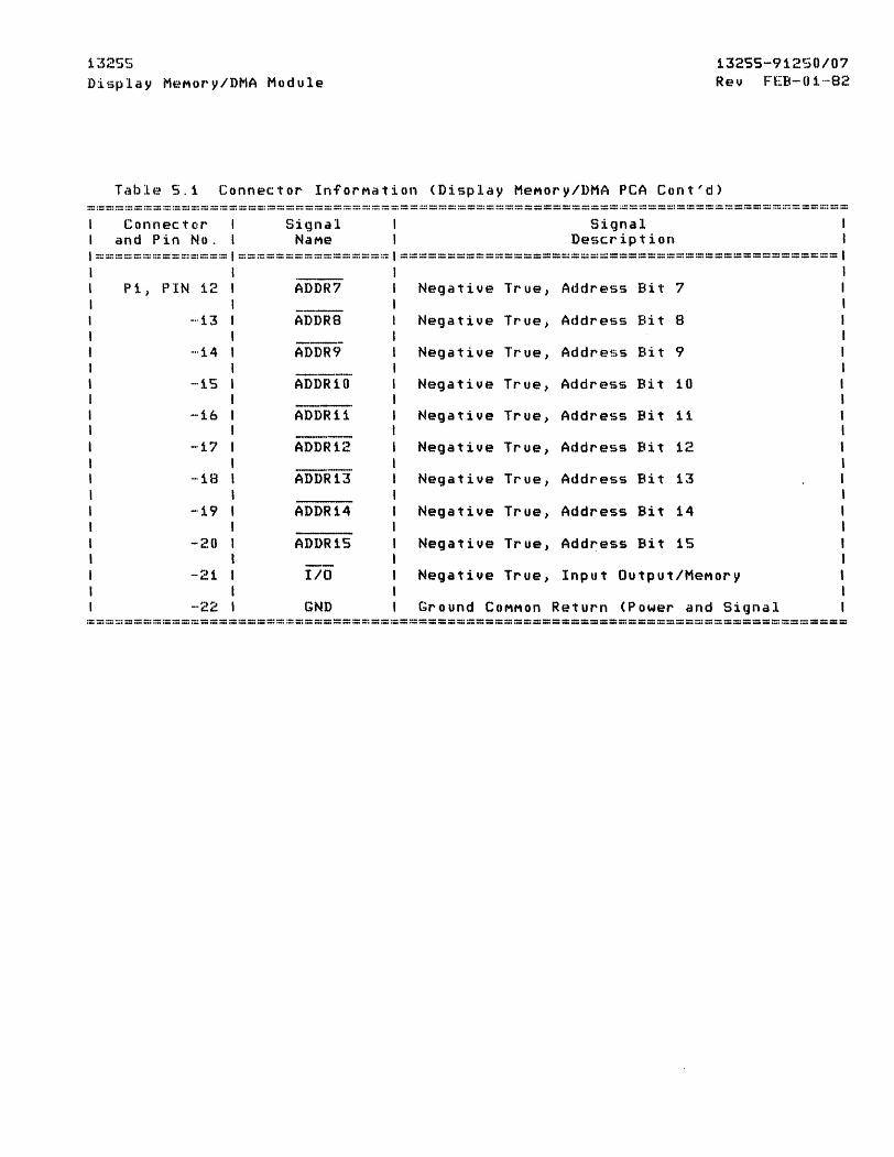
Table 5.1 Connector InforMation (Display MeMory/DMA PCA Cont'd) ~=~=============================================================================
Connector Signal Signal I and Pin No. I NaMe I Description I==========~===I================I==============================================
._--P1, PIN 12 ADDR7 Negative True, Address Bit 7
-----.. 13 ADDR8 Negative True, Address Bit 8
-----·,14 ADDR9 Negative True, Address Bit 9 -_ ...... -
-'1S ADDR10 Negative True, Address Bit 10
------,16 ADDR11 Negative True, Address Bit 11 --.--
-·17 ADDR12 Negative True, Address Bit 12
----· .. 18 ADDR 1:3 Negative True, Address Bit 13
-,19 ADDR14 Negative True, Address Bit 14
-20 ADDR1S Negative True, Address Bit 1S
--,21 I/O Negative True, Input Output/MeMory
-··22 GND Ground COMMon Return (P ower and Signal ================================================================================

i32SS Display MeMory/DMA Module
13255·· .. 9 j. 2~:> 0 to B R£~v FE.B .. ·01.·,··B2
Table 5.2 Connector InforMation (Display MeMory/DMA peA Cont'd) ===============~==========================::::::::=::::==================================
Connec tor' \ and Pin No. 1::::::::::::::::::::::::::-.::::::::::::::::::::::::::::
I P 1, P in A I I _·Ie I I I r I I · .. ·0
E'
·-F
-J
-K
-·L
--M
Signal Signal NaMe \ Description I
::::::::::::::::============\=============::::=============::::====::::=::::=::::=====::::::::==\ GND Ground COMMon Return (Power and Signal)
POLL. Negative Tru(-~) P () 11 ~~d In t £H' l' up t 1 d f~n t if i cat i () n R(:::oquet:;t
+t:?V +12 Volt Power Supply
PWR ON SysteM Power On
BUSO Negative True) Dat(~ Bus Bit ()
BUSt N~gative Tr' ue, I><~ t a Bus Bit t
BUS2 N(~gative True, Data Bus Bit 2
BUS:5 Negative True, D<~ ta Bus Bit :5
BUS4 Negative True, Data Bus Bit 4
BUSS Negative True, Data Bus Bit to" .. )
BUS6 Negative Tr Uf:~, Datc'~ Bus Bit 6 ~=::::=======::::====::::===::::::::===::::=::::========::::==::::==::::=::::===============================::::====

13255 Display MeMory/DMA Module
13255-91250/09 Rev FEB--01 .. ··82
Table S.3 Connector InforMation (Display MeMory/DMA PCA Cont'd) ================================================================================
Connector Signal Signal and P in No. 1 NaMe 1 l)escr ip t i on
==============1================1============================================== Pi, PIN N
-p
-R
-5
--T
-U
-V
-W
-x -y
-z
1 1 1 BUS7 1 1 1 I WRITE I 1 1 1 ATN2 1
WAIT
PRIOR IN
PRIOR OUT
ADDR16
ADDR17
ADDR18
REQ
ATN
1 I ,
Negative True, Data Bus Bit 7
Negative True, Read/Write Type Cycle
Negative True, CTU and Polled Interrupt Request
Negative True, Wait Control Line
Bus Controller Priority In
Bus Controller Priority Out
Positive true, Address Bit 16
Positive True, Address Bit 17
Positive True, Addr~ss Bit 18
Negative True, Request (Bus Data Currently Valid)
Negative True, Data COMM Interrupt Request ==========,======================================================================

i J;:!S~:j ~lsplay MeMory/DMA Module
132SS~"912S0/1 0 Rev FEB .... 0 j, -·82
Table 5.4 Connector InforMation (Display MeMory/DMA PCA Cont'd) :::: :~~: :::: :::: :.~: :::: :::: ;::::::: :::: :::: :::::::: ~::: ;;:: :::: :::: :::: :::: ::::::: =::.:::~: :::: :::: :.::: :::: :::: ::: :::: :::: :::::::: :~:~ :::: :::: :::::-.:::::::: ::::::::::::::::: ~::::: :.:: :.::: :::: :;!::::::::: ==::-..::;::::-.: = :::: ~-:: :::::-.:: =: =:::::::::: =:: = :-.:::::: :::: ::: :::: = ::::::::: ..
Connector Signal I and P in No. I NaM~:~
I~~==~=~=======I================ P:3 ) Pin j. GND
.-;~ I/O STr~ OHE
--3 j, O~~
'~'4 DSPCL.K ----...... _---_ ..
-·S lID SEL.ECT
-··6 AB6
-··7 AB5
--8 AB4
-('I AB:5
--1 () AB2
·"1t AS1
Signal Description
==~===========================================
Ground
Cursor Control Strobe froM Display MeM/DMA
Graphics Sync. signal--Character 103
Positive True forM of 21.34 Mhz Dot clock
NfJga t i ve T r' u e·-·· C u " s 0 r contr'ol select line
Negative True--ASCII Bi t 6
Nl~ga t i ve Tr ue·--·ASCI I Bit 5
Negative True--ASCII Bit 4
Negative True--ASCII Bit 3
Negative Tr' ue-··ASCI I Bit 2
Negative True--ASCII Bit 1 =======~========================================================================

1.3255 Display MeMory/DMA Module
1. 3255,-91250/11
Rev FEB-01-82
Table 5.5 Connector InforMation (Display MeMory/DMA PCA Cont'd) ================~===============~===============================================
Connector Signal I and Pin No. , NaMe 1==============1================
P3) PIN 1':> ,~ ABO
-13 GND
------14 MEMCYC
-15 EDROW
-16 SHFTCLK
--17 Q<~
---_. -18 SLOAD
--1 ('I VSCLK
------20 XBITS2
-21 GND
-----22 XBITS1
Signal Description
============================================== Negative True--ASCII Bit 0
Signal Ground
Clock with ~840 nsec. period defining display MeMory cycles
End of Data Row Pulse
Line Buffer Load Clock
EnhanceMent AlignMent Clock
Negative True" (Low) Indicates that CRT Controller self-load is in progress
Video Shift Clock--Line Buffer Display Clock
External Video Bit StreaM (Graphics)
Signal Ground
External Video Bit StreaM (Unused) ================================================================================

1 ~3~.~SS Display MeMury/DMA Module
132SS .... <'l12S () / 12 Rev FEB",,01····82
Table S.6 Connector InforMation (Display MeMory/DMA peA Cant/d) ================================================================================
Connector Signal Signal 1 and Pin No. NaMe Description 1==============1================1==============================================1 1 1 1 1 1 I 1 1 I __ ... " 1 I 1 P3) Pin A DSPCLK 1 Negative True forM of 21.34 Mhz dot clock 1 1 1 -B GND I I 1 1
''''C
'-D
-.. E
-- -r
-H
_ .. J
--K
--L
.. ··M
--N
.. _.p
D') I ...
GND
ZERO
CHAI~CLK
------CHARCLK
VBLANK
EBS
EB4
EB:3
EB;~
EB1
Signal Ground
Graphics Sync. signal--Dot 2
Signal Ground
Start Top-of'-Fr aMe Pulse
Charac ter' Rate Clock
Character Rate Clock (negative true)
Vertical Blanking--Graphics Sync. Signal
Positive True--EnhanceMent Bit S
Positive True--EnhanceMent Bit 4
Positive True--EnhanceMent Bit 3
Po~:)itive True--EnhanceMent Bit 2
Positive True--EnhanceMent Bit 1
===============================================================================~
1:52SS Display MeMory/DMA Module
132SS····9i2S0/1~5
Rev FEB···· 0 1····82
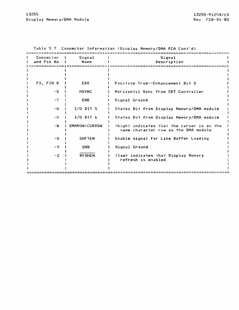
Table 5.7 Connector InforMation (Display MeMory/DMA PCA Cont'd) ~===============================================================================
Connector Signal Signal and Pin No. 1 NaMe 1 Description 1
==============1================1==============================================1
P:5, PIN R EBO
S HSYNC
-··T GND
-·U liD BIT S
··-v 1/0 BIT 6
--W DMAR OW::::CUR R OW
·-x SHFTEN
-Y GNU
-----z RFSl-IEN
Positive True--EnhanceMent Bit 0
Horizontal Sync froM CRT Controller
Si(]nal Gr'ound
Status Bit froM Display MeMory/DMA Module
Statuf:; Bit fr' 0 M Display MeMory/DMA Module
(high) indicates that the cur'~.;or is on th(~
~1aMe charac ter' l' ow c\ ":i the DMA Module
Enable signal for Line Buffer Loading
Si(Jna 1 Gr 0 und
(low) indicates that Display MeMory refresh is enabled
================================================================================

1 ~)~?S~~ 1)i~)play MeMof'y/l)MA Module
132SS-912S0/14 Rev FEB·-·01··-82
Table 6.0 Module Bus Pin AssignMents-Display MeMory/DMA peA ================================================================================
Function P~~r'for'Med : Set Cursor Y Position
Turn Display OnlOff Turn l)MA On/Off Invoke Skipeol and Mayeop Modes
Poll Bit: Not Applici~ble
Mod u Ie Addr'esto): (ADDR 11,10,9,4> - (0111)
Function Specifier: ADDRS :::: 1
Data Bus Bit IntEH'pf'etation:
8'7 (high) Indicates Display Off'
B6 (high) Ind ic:a tes DMA Of'f'
as (high) Indicates Skipeol or Mayeop Mode May be invokf~d
84 Cursor y Position 81T4
83 Cursor Y Position 8IT3
B2 Cursor Y Position 8IT2
B1 Cursor Y Pos:ition BIT1
BO Curt:;or Y Position BITO
Bus I Value I Signal I 1====::::== =::::======:==== 1 1 X ADDR 1S 1 1 X AD DR 14 1 I X Al>DR 13 1 I X ADDR 12 I
0 ADDR 11 I 1 AD DR 10 I 1 ADDr~ r:1 I X ADDR 8 I X ADDR 7 I X ADDR a I 1 ADDR S I 1 AD DR 4 I X ADDR 3 1 X ADDI~ 2 X AD DR 1 X ADDR 0
====::::::= ============ B7 BUS 7 Bo BUS b BS BUS S B4 BUS 4 B3 BUS 3 B2 BUS 2 B1 BUS 1
I BO BUS 0 1==================== 11=Logical 1=Bus Low IO=Logical O=Bus High IX=Don't Care ====::::::::::::=:::==::::::::::::::::::::=::::===
==~==::::::::=============::::====::::========::::===========::::===============================::::=

Display MeMury/DMA Module 1. ~52SS-912S 0 / is f~ev FEB-Ol--B2
Table 6.1 Module Bus Pin AssignMents-Display MeMory/DMA peA ~============================================================================~==
Function PerforMed: Set Cursor X Position
Turn Display MeMory Refresh On/Off
Poll Bit: Not Applicable
Module ~Iddr(~~ss: (ADDR 11,10,9,4) = (0111)
Function Specifier: ADDRS ::: 0
Data Bus B:i.t 1 n t e,' pre tat ion :
"87 (high) Indicates Display MeMory Ref'resh
B6 Cur'sor X Position BITb
"8S Cur'sol' X Po£;ition {<ITS
134 Cur'sor X Position BIT4
83 Cursor X Position B1T3
B2 Cursor X Position BIT2
Hi Cursor' X Position BIT1
ItO Cur~;or X Pos:i.tion BITO
Off
Bus I I Value I Signal I 1=======1============1 1 X , ADDR lS , 1 X I AD DR 14 , I X I ADDR 13 , I X I ADDR 12 I I 0 , ADDR 11 I 1 1 I AD DR 10 I I 1 , ADDR 9 I
X 1 AD DR 8 , X , ADDR 7 I X I ADDR 6 o I ADDI~ S 1 I ADDR 4 X , ADD'~ 3 X I ADDI~ 2 X I ADDR 1 X 1 ADDR °
=======1============ 87 I BUS 7 I.b 1 BUS 6 BS , BUS S B4 1 BUS 4 83 I BUS 3 B2 , BUS 2 Bl , BUS 1 BO , BUS () 1
====================1 11=Logical 1=8us Low 1 lO=Logical O=Bus Highl IX=Don't Care I =====================1
I , I I 1 1 1 1
====~=================================================================~=========

i :'5255 Display MeMory/DMA Module
3.0 FUNCTIONAL DESCRIPTION.
3.1
3.1.1
3.1.2
Refer to the block diagraM (Figure 1), scheMatic diagraM (Figures 2,3), tiMing diagraM (Figures 3,4), cOMponent location diagraM (Figure 5), and parts list located in the appendix.
DMA FUNCTIONS
The DMA state Machine interprets each byte read froM display MeMory according to the following chart:
LOGICAL DATA
Oxxxxxxx
10xxxxxx
111xxxxx or
1101xxxx
1100xxxx or
11001xxx
11001100
11001110
INTERPRETATION
ASCII character
EnhanceMent
MSB byte of link address
Software fli~g
End of line Marker
End of page Marker
Each byte froM display MeMory is latched into an eight bit register (U4S). The contents of the register are interpretted by a 256 X 4 PROM (USS) and five DMA control signals are generated (CHAR,
ENH, LINK, EOL, and EOP). If a byte is deeMed to be a character, it is latched into U2S and presented over the topplane to the Display Control/TiMing Module. For every character latched into U2S, two events occur. U49-4 is strobed by U211-8 and precharges the "shift-in" clock (SHFTCLK) used by the line buffer shift registers on the
1:32SS-9125 () 116 Rev FEB-"01"'8~?'

13255 Display MeMory/DMA Module
3.1.3
3.1.4
3.1.S
3.1.6
3.1.7
Display Control/TiMing board. The next rising edge of U24-12 causes SHFTCLK to go low, thereby shifting the next character/enhanceMent pair into the line buffers. U211-8 also strobes a Modulus 80 counter (U411 and U511) through U34-9,8. This counter keeps track of how Many characters have been loaded into the line buffers. The eightieth character causes U311-6 to go high, thereby signalling the DMA Machine to stop operation until the beginning of the next character row.
EnhanceMent bytes result in the six least significant bits of that byte being latched into U26. U26 is strobed for each enhanceMent encountered in the linked list and is cleared at the beginning of each character row and when blank fill is initiated.
An end-of-line Marker sets up a Mode in which the DMA Machine is idle, U26 is cleared, and each Machine cycle causes an ASCII 20H to be latched into U2S and loaded into the line buffers. This blank fill action continues until eighty characters have been loaded into the line buffers. The end-of-line Mode is is turned off by U711 at the beginning of the next data row.
An end-of-page Marker sets up a blank fill Mode identical to that described above except that the end-of-page Mode is not turned off by U711 until the end of the current display fraMe.
A link byte causes the DMA Machine to latch the link byte itself (MSB), and the next sequential byte (LSB) into the four counter/sequencer IC's (U12, U22, U23, and U33). A JUMP is then perforMed and the DMA Machine reSUMes operation at the "linked" address.
If a software flag is read by the DMA Machine a NOP is executed and no action taken by the Machine until the next byte is read.
13255-91250/17 Rev FEB-Oi-82
1:~2~;)S Display MeMory/DMA Module
··r ') ...J.t...
~L2 .1
PROCESSOR ACCESS CONTENTION
Thf~ Display MeMory/DMA Module operates within 840 ns cycles. At the end of the current board cycle, the outputs of the DMA control PROM's (U19 and U29) are latched into Ul10 and U210 and configures the DMA Machine for the following board cycle. If a processor display MeMory read or write is initiated, U68-8
causes the WAIT line to go low through U510-10,8 and U710-9,8, and U79-6 goes high to indicate a processor operation is pending. Halfway through each board cycle, the DMA Machine strobes U69-3 and saMples the processor status. If a processor operation is pendingi a display MeMory read or write is recognized, the DMA Machine enables bus buffers U52, U53, U54, and U44 (U44--reads only), tri-states U32, U12, U22, U23, and U33, and generates a RAS/CAS cycle. Towards the end of the board cycle, when the data transfer has been
aCCOMplished, U39-11 sets U611-6 into the WAIT "off" state, and the next falling edge of the systeM clock
restores the WAIT signal to the "go" condition. During a processor read, U44 drives the bus during the
entire duration of REQ.
The DMA Machine grants the first available cycle to to the processor operation. There are two conditions which cause the processor to be denied the next sequential board cyclej display MeMory refresh, and the execution of a link sequence. Four or five cycle burst refresh is perforMed every scan line and a processor operation during this tiMe will be delayed until the end of the refresh burst. If the first byte of a link has been read by the DMA Machine, a processor operation (and for that Matter, refresh) is held off until the second byte of the link is read and latched into the counter/sequencers.
1:3255-91250/18 Re v FEB··- 01····82
1 ~5;;~SS
Display MeMory/DMA Module
3.:3.1
4.0
4.1
4.1.1.
4.1.2
During a processor I/O operation the WAIT line is pulled low by U66-6 through U510-9,8 and U710-9,8. During the next board cycle, U79-8 generates a strobe (1/0 STROBE) that is used by the Display Control/TiMing Module to latch cursor data and Mode inforMation. lhe DMA Machine is not affected by a processor I/O
operation. The WAIT "off" condition is set at the end of the strobe through U39-10,8 and U111-11,13. The next
falling edge of the systeM clock clears the WAIT line thr'ou(jh lJ611.
REFRESH TIMING
Refresh is accoMplished in burst Mode, four or five refresh cycles occuring every scan line. Five cycles norMally occur, four cycles occur only when the DMA Machine cycle iMMediately before refresh is begun is the first half of a link. When this occurs, refresh is held off for one cycle while the second half of the link address is latched into the counter/sequencers.
HARDWARE DESCRIPTION
ADDRESS/DATA BUS BUFFERS/DRIVERS
The address and data bus buffers and drivers (U44, US2, US3, US4) are enabled only during processor display MeMory accesses. At this tiMe all other "local" bus drivers are tri-stated. The local address bus
( L A·O - LA 1 :3) and dis pIa y RAM d a t a - 0 u t bus ( LAO -LA 7 ) are pulled high, the local display RAM data-in bus
(DO--D'7) is not.
During a procesor display MeMory READ, U44 is driving
the backplane for the entire duration of REQ. The data out of display RAM is passed transparently onto the backplane and latched at the end of the current board c yc l(~~.
132SS-912S0/19 r~E~V FEB-··Ol-·B2

13255 Display MeMory/DMA Module
4.2.1.
4.3
4.3.2
4.4
4.4. i.
4.4.2
RAM ADDRESS MULTIPLEXERS
The fourteen local address lines are split into two groups of seven and each group is selected by U48-9.
The row address is cOMposed of LAO-LA7 and is changed
to the coluMn address (LAB-LA13) approxiMately 100 ns.
after RAS goes low. The row address is again restored
at the ouytputs of U42 and U43 at the end of RAS.
REFRESH COUNTER
The refresh address counter (U3S) is configured as an eight bit counter, of which only the least seven significant bits are used. The counter is strobed by the rising edge of U38-6 through U67-2,12 during
valid refresh RAS's. U66-8 deterMines valid refresh cycles and accounts for DMA link fetches during the first cycle of the refresh period.
U32 is enabled only during valid refresh cycles, and drives the row addresses only.
DISPLAY MEMORY
Display MeMory consists of eight 16K x 1 RAM's. INTEL 2117-4 or equivalent RAM's are necessary to Meet the access tiMe requireMent of no greater than 250 ns.
The data-in bus (DO-D7) COMes directly frOM the backplane, buffered through U54. The data-out bus
(LDO-LD7) is distinct frOM the data-in bus, and has several destinations: through U44 and onto the backplane, to the DMA Machine address sequencers (U12, U22, U23, and U33), to the storage latch for the byte decoder (U4S), to the ASCII character latch (U2S), and to the enhanceMent latch (U26) through a bank of inverters (U46).
1 ~52SS-912S 0/20 Rev fEB···· 01. ··82

Display MeMory/DMA Module
4.4.3
4 c· . -)
4.'::>.1
4.5.2
4.S.3
4.5.4
The hardware is configurable for both three supply and single supply RAM's. For three supply operation, load JUMpers W1 and W2, and for single supply operation, load JUMpers into the adjacent, unMarked JUMper positions. This replaceMent of the JUMpers routes +S to all supply pins except ground.
DISPLAY CLOCK (VIDEO DOT CLOCK)
The display clock (21.34 MHz) is generated by a packaged oscillator (U47). This clock rate differs frOM the first generation 264X hardware (21.06 MHz) by 1.3% and is derived frOM the following forMula:
DOT RATE = (DOTS PER CHARACTER) * (CHARACTERS PER SCAN LINE) * (SCAN LINES PER FRAME) *
(FRAMES PER SECOND) = 9 * 104 * 380 * 60 = 21.34 MHz
Note that the increase in frequency frOM the first generation 264X hardware steMS frOM increasing the nUMber of scan lines per fraMe frOM 375 to 380. This increase facillitates the use of the CRT controller on the Display TiMing/Control Module.
Nots also that in SO Hz Mode, the nUMber of scan lines per fraMe increases to 456 in order to use the saMe video dot frequency.
The display clock is buffered by U37-S,6 and U36-3,6. These two gates allow an external clock to be iMpressed upon the systeM. Grounding U37-4 (or test point "INH") inhibits the resident video clock and allows a clock of another frequency to be connected to U36-4,5 (or test point "EXT"). This port is the priMary clock input f()l~ DTS· .. ··i'O tf:~~:;ting.
13255-912'::)0/21 Rev FEB·-·O 1. ,-,82

13~~SS
Display MeMory/DMA Module
4.6
4.6.1
4.6.2
4.7
4. '7.1
4.7.2
MOD 9 CHARACTER COUNTER
The display clock is divided by nine with a high speed counter (U24). The Most significant digit (U24-11) is the character clock and pulses high once per character. This pul~;)e train is ~H:~nt over' the topplane and fed directly to the CRT controller, aMong other 1J1aces.
One half of U27 divides the character clock by two and
defines the length of the b~ard cycles (i.e. MEMCYC and MEMCYC). Each board cycle is 840 ns. long. At the
beginning of each board cycle, MEMCYC goes low and U27-9 is clocked low. The next rising edge of U24-14 causes this zero to be shifted into the serial-in/parallel-out shif'~ r(~(.~istE-?r (U3B). The appearance of a low value at U38-3 (the first shift position) presets U27-9 back to the high state, where it reMains until the beginning of the next board cycle. The next seven riSing edges of U24-14 cause this low state to progress frOM U38-3 to U38-13 and effectively create eight clock phases in each board cycle. These eight phases are used to create all MeMory tiMing and control the operation of the DMA state Machine.
RAS/CAS GENERATION
MeMory tiMing in this Module is relatively conservative, Most events occuring on even 8S ns. intervals.
If a MeMory cycle is pending) U110-2 (MeYC) goes low just prior to the first character clock in a board
cycle. This allows U38-3 to strobe RAS (U48-4) low through U28-12,11. ApproxiMately 8S ns. later, U38-4 goes low and the row address is changed to the colUMn address through U48-10,9. as ns. after the address
swap, CAS is brought low by U38-S through U28-10,B and U4B-·S,7.
When a low levf:d is shiftf.H.1 into U3B-10, RAS is brought high, and the row address is restored to the outputs of the address Multiplexers. This tiMing allows
132SS-(] 12'::> () 122 R (.:~ v FEn··· () 1. ,-,02

Display MeMory/DMA Module
4.B
4.0.1.
4.8.2
4. B.:3
4.B.4
4.B.S
4.8.6
for a very long RAS precharge tiMe, and is arbitrary as far as the RAM address goes.
CAS returns to a high state as a result of the first character clock (U24-11) of the next board cycle through U410-1,3 and U48-6,7.
MISCELLANEOUS BOARD CYCLE TIMIMG
Qd, the signal at U38-6, occurs in the Middle of a board cycle. It is used for general tiMing at U510-13 and U69-3 and to Mask the second character clock in a board c:~'clE~ at U410-2.
The saMple clock (U38-10) will pulse low 200 ns. after
CAS goes low. The data at the output of the RAM array is latched into U4S and U2S with the saMple clock.
The increMent clock (U38-11.) strobes the MOD 80 character counter (U411/US11) through U310-3,1, U211, and U34-9.B. This clock phase also releases the "processor' wait" Mode through U78-1,~~, U39-j.3,11, U111-12,13, and U611.
The video shift clock (P3-19 and U49-9) is basically a train of eighty 200+ ns. pulses. This pulse train is synchronized by P3-X and is used by the recirculating line buffers in the Display TiMing/Control Module.
DOT 2 (P3-C and U28-6) is a synchronization signal used by the graphics board set (02640-?1??? and -1?11?) and aligns the graphics output within the character cell. Care Must be taken that a negative edge of P3-A
occurs during the active low portion of DOT 2 for proper graphics Module operation.
The next state clock (U310-10) is a positive pulse at the end of each board cycle. This clock strobes the registers of the DMA state Machine (U110, U210, and US7-11) and configures those devices for the upCOMing board cycle.
1. :"5255'-912':> () /2:3 R E~ v F [It _ .. () 1 .... 8 ~~

1 :5;:'~S~:) Display MeMory/DMA Module
4.<7
4. (y. 1
4.9.2
4.9.3
4.10
4.10.1
4.10.2
DMA ADDRESS SEQUENCERS
Dir'f.:oct ME~Mor'y aCCf?SS addf'ess sequf.mcing is perforME~d by four 2911A integrated circuits (U12, U22, U23, U33). Th(·:~se i:H'f:~ four bit'-slice, bipolar', 60 ns. par'ts--Good Stuff! See SOMe National or AMD spec sheets for dE~ti:\il~) .
The DMA address is forced to zero at the end of each fraMe by the action of P3-J (vertical blanking) through
U57-3 and pin t9 (ZERO) af each 2911A. This physical 0000 Maps into a logical FFFF through the inverted bus structure. In fact, The binary "up" counter internal to the 2911A sequencer beCOMes a binary "down" counter with the inverted bus. It is with these counters that the DMA address sequencing is perforMed.
During link operations, the bank of 2911A's fetches the two bytes of a sixteen bit link address through the external data port (pins 4,5,6,7 of each 2911A). Contl'ol s;ignal JUMP (USB-B) causes the latched data to be iMpressed onto the local address bus resulting in a sequencing "jUMp" to the link address.
ZERO ADDRESS GENERATOR
The start of vertical blanking forces U57-S low and US7-6 (P3-E) high. These signals force the DMA address to 0000, reset the DMA Machine to top-of-fraMe, and clear the DMA row counter in the Display TiMing/Control Module.
The zero signal is returned to its inactive state with the first 2911A clock of the fraMe through U34-3,4. The riSing edge of this clock latches the nOllO aclclr'(·~~:>~:> in~;j.clE~ the ;:?(~lj.A and thEm l'f::tMOVeS the zero condition so that proper address sequencing can be pel'f'or'Med.
132SS-912S 0 12.«, Rt:~IJ FEB···Oj.···S2

13;~SS
Display MeMory/DMA Module
4.11
4.11.1
4.11.2
4.11.3
4.11..4
4. ii. S
HSYNC SYNCRONIZATION
HSYNC (P3-S) is a signal sent frOM the in the Display TiMing/Control Module. occurs once per raster line within the retrace interval, and is used to force state Machine into MeMory refresh Mode.
CRT controller This signal horizontal the l)MA
The CRT controller does not allow for specific start-up states (i.e. ther are no preset or clear capabilities). As a consequence it is iMpossible to deterMine the exact alignMent of HSYNC (nine char. wide) within the two character wide board cycle.
The circuit consisting of U69 (FFt2), U79-1,2,3 and U59-1,2 , 3 guarantees that the output signal, U69-9, is aligned properly within the board cycle.
In the Mid ell e 0 f abo a " d c Y c 1 e, ME M C Y C (] 0 e 5 h i 9 h . When HSYNC is present, U69-9 is clocked high by
MEMCYC. When HSYNC returns to its inactive state,
the next low level of MEMCYC clears U69-9. This alignMent provides proper synchronization between the DMA state Machine and the hardware it controls.
A high state at US9-8 (HSYNC+SLOAD) indicates that a burst refresh period is pending. If a link is not being fetched by the DMA Machine, the board is configured into refresh Mode. If a link is being fetched, this configuration is held off for one board cycle with U66-9 and the state Machine logic.
After burst refresh has been accoMplished, HSYNe, US9-8, U57-9, and U66-8 beCOMe sequentially inactive, and the board is configured for DMA and processor operations.
1 ~12SS-9 1. 2S () 12S 1~0~1J FEH-() l. .... Bi!

13255 Display MeMory/DMA Module
4.12
4.12.1
4.12.2
4.13
4.13.1
ASCII AND ENHANCEMENT STORAGE LATCHES
These two devices (U2S and U26) are used to store character data frOM display MeMory and present this data over the topplane to the Display TiMing/Control Module. U2S is strobed by the saMple clock (U38-10) every board cycle. The enhanceMent latch, U26, is strobed by the increMent clock through U78-1~2 and U410-10,B only when an enhanceMent is fetched frOM MeMory as deterMined by U28-1,2,3 and U61-3,4,S,6. Characters are stored in U2S in COMpleMented forM and enhanceMents are stored in true forM through the action of the inverter bank of U46.
When a character is fetched frOM MeMory, U2S is loaded with that character, U26 already contains the proper enhanceMent. A strobe is sent over the topplane shifting this character cell data into one set of the r~circulating line buffers in the Display TiMing/Control Module.
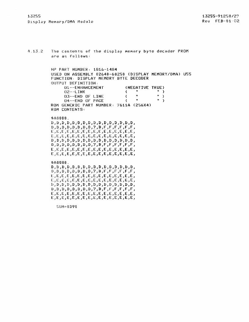
DISPLAY MEMORY BYTE DECODER
The display MeMory byte decoding circuitry deterMines the type of data fetched during each DMA board cycle. U4S is strobed by the saMple clock, and its outputs are iMpressed upon the address lines of USS, a 2S6X4 PROM. A character byte causes USb-iO,S to go high, thereby disabling the PROM outputs. All other types of MeMory data are decoded by the PROM and the proper output is brought low. These outputs configure the board into the proper Mode to respond correctly to the byte that has been fetched.
13255-91250/26 Rev FES-U1-82
Display MeMory/DMA Module
The contents of the display MeMory byte decoder PROM cH'~:~ a~:; 'fo 11 ows:
HP PART NUMBER: 1816-1484 USED ON ASSEMBLY 02640-60250 (DISPLAY MEMORY/DMA) USS FUNCTION: DISPLAY MEMORY BYTE DECODER OUTPUT DEFINITION:
() ji. ·"····[NHANCEMENT O~~· .. · ... L.. I NI< U::~-""·END OF I... I NE D4······ENI> OF PACE
ROM GENERIC PAI~T NUMBER: I~()M CONTENTS:
(NEGATIVE ( ..
( ..
( " 'l611A (2S6X4)
$(~OOO() . D,D,D,D,DiD,D,D,D,D,D,D,D,D,D,D, D,D,D,D,D,D,D,D,7,B,F,F,F,F,F,F, E,E,E,E,E,E,E,E,E,E,E,E,E,E,E,E, E)E,E,E,E,E,E,E,E,E,E,E,E,E,E,E, D,D,D,D,D,D,D,D,D,D,D,D,D,D,D,D, D)D,D,D,D,D,D,D,7,B,F,F,F,F,F,F, E 1 E,E,E,E,E,E,E,E,E,E,E,E,E,E,E, E,E,E,E,E,E,E,E,E,E,E,E,E,E,E,E,
$('~(}OBO . D,D,D,D,D,D,D,D,D,D,D,D,D,D,D,D, .t),D,D,l),D,D,D,D,7,B,F,F,F,F,F,F, f,E,E,E,E,E,E,E,E,E,E,E,E,E,E,E, E,E,E,E,E,E,E,E,E,E,E,E,E,E,E,E, D,D,D,D,D,D,D,D,D,D,D,D,D,D,D,D, D,D,D,D,D,D,D,D,7,B,F,F,F,F,F,F, E,E,E,E,E,E,E,E,E,E,E,E,E,E,E,E, E,E,E,E,E,E,E,E,E,E,E,E,E,E,E,E,
~~ U 11 ::: () D 9 0
TRUE) .. ) .. ) .. )
132SS-912S()/27 R f~ IJ FEB··· () 1··D2
Display MeMory/DMA Module
1\.14
4.14.1
4.14.2
4. is
4.1~~.1
DISPLAY MEMORY BUS DECODING
In the 264X MeMory Mapping scheMe, display MeMory resides in the top 16K bytes of a 64K address space.
(i.e. ADDR 14 and ADDR 1S are physically 00). In the first generation 264X hardware (i.e. 2642A and ei:lrl:i.er Mod(~lf:), P1--V,W, and X ar'e bottoMplane contention and arbitration signals. The second generation hardware reMoves this contention and uses these three bottoMplane lines as address lines, essentially giving the terMinal a total address space of 8 tiMes 64K bytes. Within this scheMe, display MeMory resides in the top 16K bytes of the bank accessed when P1-V,W, and X beCOMe physically 111. When using this board set with the first generation hardware, the switch bank at U18 should be set to all n0pen" causing this Module to ignore the bus contention signals. In the 2647F, this switch bank should be set to all IIclo~;ed" in or'd(-?r to r'espond to the di~;play/IO banl< only.
The pertinent signals generated by this block of ... __ ._-
circuitry are U6B-B (MEMSELECT) and U710-11 (uPREAD). MEMSELECT indicates that the processor is accessing
display MeMory and uPREAD indicates that the processor is perforMing a display MeMory read. This latter signal enables U44 to drive the bottoMplane data bus with the iy\€,MOl'y data·-·out.
CURSOR CON1ROL BUS DECODING AND CRT CONTROLLER STROBE GENERATION
Cursor control is achieved through two 1/0 ports, one for cursor colUMn and one for cursor row. A processor 1/0 write to either port CiHJSeS P3-"S (U66-.. 6 (H'
I/O SELECT) to go low. P3-S sets up the proper CRT controller address for cursor control and eventually allows U24-i2 to generate an I/O STROBE on P3-2 through U'79·· .. <1' > 8.
1 ~32SS-(',12S () 12B Rev FEB--l}:\. -02
Display MeMory/DMA Module j. 3255-(~ 1. ;~'::) () 129 R(~v FEB···Ot···S;?
4 .16
4.1.6.1
4. j.6. 2
4.16.3
BUS INTERPRETATION AND WAIT GENERATION
This portion of circuitry essentially synchronizes the processor (with its 4.9i5 MHz. clock) with the display MeMory cycles defined previously. In order
to do this successfully, the WAIT line (Pi-S) is pulled low iMMediately upon the decoding of either a display MeMory access or an 1/0 access. This causes the processor' to go into nUM(-?rou~; "wait ll statf?S whilf? this Module cOMpletes its present actions and prepares for external interaction.
Upon the receipt of either MEMSELECT or 1/0 SELECT, US10-8 goes high, P1-S goes low and U79-i1 goes high. Halfway through each board cycle, U69-3 is strobed and the processor status is saMpled. If a processor operation is pending, U69-S will go high and U69-6 will go low.
If it is a display MeMory access that has caused this, U79-6 will go high, signalling to the DMA state Machine that the processor wants into display MeMory. This status line is saMpled several hundred nanoseconds later by the DMA stat(-? Machine to allow for possible "l'unt" pulses at U69-S due to the lack of proper setup tiMe at U69-2. The saMe delay is true for the liD STROBE. If an lID write is pending, the DMA state Machine doesn't care and Ui11. goes high, allowing an I/O STROBE to be generated on P3-2.
:t ~5 ;.~ ~:) ~j Display MeMory/DMA Module
4.16.4 The cOMpletion of a display MeMory access is signalled by U39-11 going high. The cOMpletion of an 1/0 write is signalled by U39-8 going high. Either of these events causes U611-1 to be strobed through U111-11,12,13 and U611-S will go low and U611-6 will go high. A low state at U611-S clears U69-1 and disables the processor status line and the lID STROBE. The high state at U611-6 is clocked into a low state at U611-9 by the next falling edge of the systeM clock (Pl-3). U611-9 going low
causes the WAIT condition to be released, allowing the
processor to proceed on its Merry way. When REQUEST
(Pi-Y) is brought high by the processor, this WAIT generation Machine is priMed for another processor a(::cess.
PROM DRIVEN DMA STATE MACHINE
The DMA state Machine consists of two 60 ns. 2S6X4 PROMs and two schottky latches. The address lines of the PROMs are the basic status lines of this Module and convey such inforMation to the DMA state Machine as the present Mode of operation, fraMe tiMing, processor status, and refresh tiMing. U29 is the cycle arbitrator and deterMines whether the pending board cycle is a processor operation (uPOP), a norMal DMA cycle (DMACYC), or a DMA link operation (DMACYC and RE1). lH.9 c:ontrol~;) the special DMA Modes. Its outputs are end-of-line (EOL), end-of-page (EOP),
i32SS-912S0/30 Rev FEB-01-82
.o.i. ~:~p 1 ~:i y Mf.~lvl 0 r' y 11)t'1A M () c\ lJ 1 e
4 . ~1. 7 . ;:!. lhe contents of the two DMA state Machine PROM's are as follows:
HP PART NUMBER: 1816-1485 USED ON ASSEMBLY 02640-60250 (DISPLAY FUNCTION: DMA CYCLE ARBITRATOR
MEM()I~ Y IDMA) U~?'9
OU1PUT DEFINITION: OJ. ·····_·DMA CYCLE (POSITIVE O~? .-.. _. M I C R 0 PRO C E S S 0 R eye L E ( "
(NEGATIVE 03--M~MORY CYCLE 04--REGISTER ENABLE
ROM GENERIC PART NUMBER: r~OM CON rENTS:
1 (POSITIVE 7611A (;'~S6X4)
$t-d}OOO. C,C,C,C,9,9,C,C,C,C,C,C,9,9,C,C, 4,2,4,2,1,2,4,2,4,4,4,4,4,4,4,4, c,C,C,C,9,9,C,C,C,C,C,C,9,9,C,C, 4,2,4,2,4,2,4,2,4,4,4,4,4,4,4,4, 1,2,4,2,1,2,4,2,4,4,4,4,4,4,4,4, 1,2,4,2,1,2,4,2,4,4,4,4,4,4,4,4, 4,2,4,2,4,2,4,2,4,4,4,4,4,4,4,4, 4,2,4,2,4,2,4,2,4,4,4,4,4,4,4,4,
$t-d)()80.
4,4,4,4,1,1,4,4,4,4,4,4,4,4,4,4, 4,2,4,2,1,2,4,2,4,4,4,4,4,4,4,4, 4,4,4,4,1,1,4,4,4,4,4,4,4,4,4,4, 4,2,4,2,4,2,4,2,4,4,4,4,4,4,4,4, 1,2,4,2,1,2,4,2,4,4,4,4,4,4,4,4) 1,2,4,2,1,2,4,2,4,4,4,4,4,4,4,4, 4,2,4,2,4,2,4,2,4,4,4,4,4,4,4,4, 4,2,4,2,4,2,4,2,4,4,4,4,4,4,4,4,
TRUE) II )
TRUE) TRUE)
13;:~SS-912S () /31 rh:~..., FE.B-- 0 i-B2

1J2SS Display MeMory/DMA Module
HP PART NUMBER: 1816-1486 USED ON ASSEMBLY 02640-60250 (DISPLAY MEMORY/DMA) U19 FUNCTION: END OF MODES CONTROL OUTPUT DEFINITION:
01--END OF LINE (POSITIVE TRUE) 02--END OF PAGE (" " ) 03--SKIP END OF LINE (NEGATIVE TRUE) 04--END EOl OR EOP (" " )
ROM GENERIC PART NUMBER: 7611A (2S6X4) ROM CONTENTS:
SAOOOO. F,E,D,C,F,E,D,C,6,E,4,C,6,E,4,C, F,E,D,C,F,E,F,E,6,E,4,C,6,E,6,E, F,E,D,C,B,E,9,C,6,E,4,C,2,E,O,C, F,E,D,C,F,E,D,C,6,E,4,C,6,E,4,C, C,C,C,C,C,C,C,C,4,C,4,C,4,C,4,C, C,C,C,C,C,C,C,C,4,C,4,C,4,C,4,C, C,C,C,C,8,C,B,C,4,C,4,C,O,C,O,C, C,C,C,C,C,C,C,C,4,C,4,C,4,C,4,C,
SAOOBO. S,4~D,C,S,4,D,C,4,4,4,C,4,4,4,C, S,4,D,C,S,4,D,C,4,4,4,C,4,4,4,C, S,4,D,C,1,4,9,C,4,4,4,C,O,4,O,C, S,4,D,C,S,4,D,C,4,4,4,C,4,4,4,C, 4,4,C,C,4,4,C,C,4,4,4,C,4,4,4,C, 4,4,C,C,4,4,C,C,4,4,4,C,4,4,4,C, 4,4,C,C,O,4,B,C,4,4,4,C,0,4,O,C, 4,4,C,C,4,4,C,C,4,4,4,C,4,4,4,C,
SUM=OBA8
132SS-91~SO/32 Rev FtB-01-82

13255 Display MeMory/DMA Module
13255-91250/33 Rev FEB-Ol-82
4.18
4.18.1
4.19
4.19.1
CHARACTER AND BLANK FILL SHIFT CLOCK GENERATOR
The line buffers resident in the Display TiMing/Control Module are loaded with a row of characters under the control of the Display MeMory/DMA Module. When a valid ASCII character is "DMA'ed" froM display MeMory, U211-8 will go low through the action of U211-1,il,12,13. When blank fill Mode is invoked (i.e. under end-of-line or end-of-page conditions), U111-4 will go high, U2S will be loaded with an ASCII 20H (blank) every DMA cycle, and U211-8 will go low through the action of U211-4,S,6. U211-8 goes low as a result of INCClK (U38-11) through U310-3,i. This clock COMes late in a board cycle. The low state at U211-B strobes the eighty character counter (U411 and US11) through U34-9,8, and presets U49-S to a high state. U49-S goes directly over the topplane to the Display TiMing/Control Module and deterMines when a valid character/enhanceMent pair is loaded into a line buffer. The actual load occurs early in the following board cycle, when U49-S goes low through the action of Qc (U24-12). Note that U49-6 is fedback to this clock generator through U37-13,11, U78-11,10, and U310-2,1. This circuitry prevents errant clocking of the eighty counter as the decoded outputs of U411 change states, particularily at character sixty-four.
EIGHTY CHARACTER COUNTER
The eight bit counter Made frOM U411 and US11 counts the nUMber of valid character/enhanceMent pairs that have been loaded into the line buffers in the Display TiMing/Control Module. The count is increMented by U211-8 as described above. When a count of eighty has been reached, U311-6 goes high frOM U411-14,12 and U311-4,S. U311-6 (aO) is a status line to the DMA state Machine. When U311-6 goes high, the DMA state Machine discontinues direct MeMory access because eighty characters have been loaded into the line buffers. Direct MeMory access is restarted at the beginning of the next data or character row as indicated by P3-1S, EDROW (end of data row).

1 :~ ;:~ ~:) ~:) D i ~~ p ]. a y r1 (~~ i''I 0 (' y / 1) M I!:) M 0 cI u I £~
i ~"52SS-9 12':3 () /34 f{ev FEB-'O 1-,02
4 . ;:!.O
4.t~O.1
• JUMP TO LINK ADDRESS COORDINATION CIRCUITRY
The circuit block M~de up froM US8, 1/2 of U711, and 1/2 of US10 controls the sequence of events that are necessary to fetch a link address froM display MeMory and p<-?r'for'M i:\ II JUMpll to the fetched iitddress to begin direct MeMory access at the link address. The events are very specific and exact and are defined as follows:
1) a link byte is read froM display MeMory as identified by its characteristic code,
;:~ ) t tH:~ 1) MAs) tat e Mac h i n E-~ 9 0 e 5 in t 0 a Mod e b y which the link byte and the next sequential by~e of display MeMory are latched within the DMA address sequencers (U12, U22, U23, and U33),
3) upon latching the second byte of the link address, the address sequencers are configured to iMpress the internal latch contents onto the display MeMory address bus (as opposed to the internal increMenter contents as during IInorMal", sequential DMA),
4) the first DMA cycle iMMediately following the latching of the second address byte is perforMed at the link address and a JUMP has been cOMple-~ted .
When a link byte has been fetched frOM display MeMory,
LINK (USS-11) will go low, U29-9 will go high, and during the following board cycle U210-7 will be high
and U210-6 (RE1--~egister enable t1) will be low.
REi being low causes ~he display MeMory link byte to be latched into U23 and U33 on the rising edge of the 2911 clock (U311-8), and presets U711-8,9
(LINK" and LINK") to states that indicate to the DMA state Machine that a link operation is being perforMed. REi is delayed by one board cycle (U210-7 to U210-4) and creates the signals RE2 and
RE;~ (U~~tO--2,3). Thf~ IH1A statf~ Machine t'(~tchE-:~s the next sequential byte frOM display MeMory and this byte is latched into U12 and U22.

Display MeMory/DMA Module 1 :3255-9 j. 2':) 0 /35 Rt:~v FEB-01-B2
4. ;:!.l). 4
4. ;::~U . S
4.?1.1
4.i!.1 .. ~~
RE2 presets US8-6 indicating that both bytes of the link have been fetched and latched. USB-11 is clocked the beginning of every DMA cycle. The norMal state of U58-6 is high such that "norMal" DMA cycles are perforMed with US8-8 (JUMP) low. Once US8-6 is preset low, a high state gets clocked into USB-8, and the first DMA cycle following this event is perforMed ur:=,:Lng th(o:~ latched 1inl< byt€·~~:) a~) thE~ DMA addres~:> instt:~ad of th~? "norMalll inCr\eM€~nte~\ address of the 2911's.
As this JUMP is perforMed, U58-9 clears USB-6 back to the non-JuMp state, and U711-11 is clocked through the two gates frOM U510. This reMoves the LINK" signal frOM the input of the DMA Machine, and allows the state Machine to continue with "norMal" DMA.
Note that events can occur between the latching of the second link byte and the actual JUMP such as display MeMory refresh and processor MeMory access. Also note that U711-B keeps the second byte of the link frOM being interpretted as a character through U211-13.
SKIP END-OF-LINE CIRCUITRY
The skip end-of-line circuit prevents the DMA state Machine frOM Misinterpreting the software data structure as the processor is adding characters to the screen. Two status bits iMbedded in the "cursor row" byte latched in the Display TiMing/Control Module (I/O BITS and I/O BIT6) indicate when a skip end-of-line operating Mode is applicable. When skip end-of-line Mode is invoked, U19-10 and U110-1S will go low and preset U610. EDR (end data row) saMples the status of U610-9 through U410-13,12,11 and if EOL's are to be skipped, U610-S,6 will be preset. These outputs prevent the DMA state Machine frOM reacting to EOL's ( US 6 .... 1. :t ) 1 ;:.~ ) 1. 3» c: h i:"Jr' ~\ c: ·t ~~ r' s (U 31. 1. '-' 1. ) (? ) 3), and
(7~' II han c: (~! M (~n t ~:~ ( U? B "-1 , ? , 3) .
Skip end-of-line Moded is turned off when a link is fetched that points to the beginning of the next row on the screen. 1h1s is indicated by the least significant nibble of the link address being 1111. Under these c. i l' c: U IVi S tan c E-~ S) U 6 S -- 6 wi 11 g 0 h i g h, and LJ 61 0 - S , 6 will be clocked to their "norMal" 5t.ate when the second reqist(~·~r enable signal (RE2) goes high.

IO'Of;~ ... rE------I
r ~AJ(;.I(1)N'i"RD'-
n~1cN~ .. ~~0f4 ,I- K. i~~
"t/I-S"LAY
r1f14Dl~
fiS/as C'"'I€I(£A/In ON
~
• I 1
~£f~St' ~CS\TO~E.
C.>N'foL I t4fft.f' "c. E
t
r I
bMA 5111"r€
-- t"ft.~H£
I BoK€
\~,~~er~
,
~\oP.A'E
lATCJtE:S
~ 'rO YI$P/,.A-1
1"1 ~ I N G, / C i>tlT({J) L.--
FIGURE 1 02640-60250 BLOCK DIAGIRAM FEB-01-B2 13255-91250

£1)4£
COUNUnON
r
i
I
I I
I I I l __ _
[ z-C-1
;z-1>-2..
Z-A-l
( ?\-c
ON80~t:l C,.oA!N&GnOt.l
( xl( -X)( )
C~f-~-f'I~
IX-x-IC I ~~ - 'I.lOlcft>t/IAT'E. - ~. ca&ll!.l>n(ltrE
z x
• -5V
'l.7K
j""'r'l1"(% M~I('£.D 1"D~ "3 ~"""-~ ~~.
$,J./EiLf S~Pl'( O~AT1\)t.\ ~['QIlIII:f.'$.
Rf?oS',TIONIIIlEi j"')""~(l!;. ONL..'1.
"",""nES:
Y,,-I.St71 '7f,,-L'io 38
'/~-I.'Sn
IJ~ - I-SO"l
r----------- - - I
,"e-,~ .. ,I'l 1.4'110- 1,'2,1.i"'i~"
IAS'I- ",'-,to "79- ~I"'\
I
I
LOC."'L Ai>i:>I<:e~ ... 91X (~-[Aj3)
FIGURE 2 DISPLAY MEMORY/DMA FEB-Ol-8;~
-
1 'I"'t
cS: 470n <;> RI4
2-"8-1 I
24>-1 I
SCHEMATIC (PAGE 1) 13255-91250
I
1(<:o?t.l ~2'5 +5m
( 1'3- $
~ CIlHH£C;rDll(
( XX- XX ) c. .. ~- ,., ..... ~
FIGURE 3 DISPLAY MEMORY/DMA FE})-01-B2
p, -vJ )
)
)
SCHEMATIC (PAGE 2) 13255-912S0

T flJlll:o.lt = 21."51"'11.
:. T ~ .. -: 1t1Sec..
PSPCI.\( r 3 -1
Q" ~T\~. Y'!- 1'7
Q~ \~ r, , ,
: / , \ 1A~-13 r, '-I
Qc \J. ,t? 14"-~
C~CLII. n-F
MEi1m \ 1?-H \.
nil 1.138-3
Q!I u3&-i
Qc 1.138-5
Q'D
1A38-G
QE. SAHPLE CLOCK.
~'38-IO
Qf INC~9'lENT CLOCK 1.439-1\
Q" /'--j \.l~-It.
NSC.LK. \
lA~IO-IO '-
"AS Li18-1
O,S r---
/J1S-1
Row/C(XvMN
WI~-~
AAt1.J1I71')K f(ol'\ \.1411. , ~4>
Row ""~1t. VAL.II:>
'RA~ l:*TIt ollf \)A,"'~ OVT VAI-IO
",~TATE
!.All - 1).8 I
rr ' l t7 \\ /""/ \ \ ~ L' u '-\ ~ I
\~ /7
,---I
COL.vt4~ "'l>~E-$';
'R ..... t1 PATA COT VALID
~ \ I \ , L I-
\~ /7 \ \ \ .... ' //
l I
\~ /7
, '----
, ~----
,---I
I \ \- ----
\ L _____
MW~ ,<,,,WI> COL.ut'lN "l>Dll. "~L.lt:>
7'1t1"iTATE
FIGURE 4 DISPLAY MEMORY AND MISC. TIMING FEB-01-B2 13255-91250

I.
1L
t'\£.t1tVC 'PEFIN£S THE Lcij~TH Ot:' ONE "8D A"RD C. ,(CL.E
( ® tc @ * ONE C(C.t.E)
U3B (LS 1"4) IS USE'D ro G~E'R.A-rE SEVEN C.LD'-K. 'PHA~.r; ()S~." "10 c..oNnOL ALL 'BoARI::> TIt1lN~.
@ THIS Et>~E '5T'r'Krs ~AS
© n-HS ~E swAPS "Rovv ANP
tDl-uM'I\' AD"DKE<S~ES
@ Tit'S t:.~E.. -5"fM?iS CAS
® 1'tf1"; 1--0W ~1d1PL.eS ~A11 1> 1Yf'+ ou""
® m{? l-Ow cS ,()flS Kl6 IrNO "RDw/C1Jt..JMN. lIJC"f~~NT.s
£Ie-I+'i'l' c..t+~c.,..,e. c..ovl-\T'i 12.....
© Tit l-=> 1.-0 vJ G ~~I<A~ N ~ C.lA<-
TIMING DIAGRAM TALK ONLY
I
GLITCH D+SPLAY [ON ] MAGNIFICATION [X,10] I
I I I. 1 I
TRACE-COMPLETE
50NS/CLK 100NS/DIV
[ 00. ONS] , I ,
o ®~/. I -®~~ __ _ 1 ---®---r-q_ J -. --- --- --- -- --------~_ ._ ------- -l r------ - ------------- - --'----
2 ©~-_J ------------1 ---1 r- ---- ---.- - - ---- - - - -- --
3 @~L_J 1 - ----- 1 r -- - "-_ .. -- - --. - - -- -
4 i- ___ j
1
~ r -- - - - ---- -®~, \
L_J
L~'CA Ov'T'F\JT~..) ",
U!9- ~
SAt-1t'LE. LL-I(.
/).'39 - 10
,
sLf-----------------®{_T - -- - - -"J~';'.IO~'~ <.W<I<-
1
7 I I' L-J
---------------- --~ 1 r -- - - -®,-...~ _ j 1.f!8 - 1"2-
FIGURE 5 MISCELLANEOUS BOARD TIMING FEB-01-B2 13255-91250

I. M04\t'lt. AND M~MC.'1'c.. *F''''E THE.. LENGTH OF A BoA~l) HE Mu1<'i C."?C.LE'.
( @) t.o @ ~ ONE.. C~C.L.E )
][. lE.NqTf.! DF CA~ HOLDS 'KA.t-J\ 1:>A,I\OUT VALID TI-\-':::o.)~~ "DLF:htoN or f5o~'R? c. it L'E .
JII.., N5CLK SiftNAL5 T»E. END of A. BoARD C:(C.L£.
ND D2 I~ A '6YNCr\KDN1"ZATI~ "SIGNAL-
10 Ttt€= G1<'A?"lc..~ ~ONl,.,E
TIMING DIAGRAM TALK IONLY
TRACE-COMPLETE
SONs/eLK GLtrcH DISPLAY [OFF] i00NS/DIV
I M4GNlrIC~TIO~ [~10] J I I [ 9o·0~S] I
o ~'rll....-.j ____ ~nL __ -_~._ @_2iJ'1 ___ c~:~ 1 I r----------~--l ~~Mlv(..
&..... _______ ---1, L_~____ u%.1-~
------1 [---- M~c.ic-
L ______________ . uZ1-t.
3 -1 r--~·-·--·-·--l ~
L-_- __ J L.__ u.~9-~
4 'I ,--- Row/ COW~N - ~ (,\~-,
5 I -----, '[---56 6 rl L ---------rl- IJs:'7
--J L ______ -___ -_-_____ -__ J L __ .~ ___ U'310-tO
I -U--------- -U--------~-- ~'2S- C. 7
FIGURE 6 RAS/CAS GENERATION FEB-01-B2 13255-91250

1:. ~K-f"Ta1 1<orJ~IiL-'" GoR~E'5~1>S -'-0 t+~, l-ct-JTA.L 'Ke:T~L E... ?~:i( lOP,
'tc, tr5Y~c. COM.SoS ~OM CRT LoN11<OLlr£R..
\N P\S'7t-A'l TIM( ,,\~ I Lol-ri{COL Y"'to"D\JL.E.,
~-SYN C. 1=i1RcES TttE 1>MA S,ATE
t1ACt4If'J~ 10 VO M£i'1c>R'i ~EFR£~t-l
.:nI, VSCLK IS vSE~ ~'i --~E.. ;;'\S"PlA\-i
TIM I N ~ I LON TG( () L... M o"D 0L E 1"" 0
R€.c"'R.C.vLATE c~tAeACTE.tZ. 'DATA fUR
VI"?€Q \7\S"PLA'i
I
TIMING DIAGRAM TALK ONLY EXPAND INDICATOR [ON ]
GLITCH DISPLAY [OFF] MAGNIFICATION [I Xi 1
I I I I I ,
TRACE-COMPLETE
50NS/CLK 1US/DIV
[ 100 .,ONS1 o l-..... I----- rv ~oRl~oN.,.~L 'R~T<2"""f_ -I SHFTE:kl
~-'(
1~t---_----ruuuu v~c..I-\<'
~~"1
~y~c ?'3-S 2 II ~ ________ __
3 I I I I I I I I I I I I I I 4 I I 5 Lru 8
7 ___ rLnJ
N~t...1( U3iO-'O
1( F5ti , tQJI.rr. ~ (A",,-e
~ ()4f~-~
~F'~tf .A't>t>R. C.L~ U~1-1'L
L.~a of' ~~ ... ~, CJ.l'1t CA'M-5
FIGURE 7 REFRESH TIMING (A) FEB-01-82 13255-91250

:II I t+S~NC CAJC;SS 'R~~REs f4 10 occ UK -Pu«If',i(l c:A/_+-i t!)(( tOf'l-rAL-
'R E-,Me £- '? E P. 1 :> 'D.
TIMING DIAGRAM TALK ONLY EXPAND INDICATOR [ON ]
GLITCH DIS~LAY [ON ] MAGNIFICATION [Xi 1
I I I I I I - "1
TRACE-COMPLETE
250NS/CLK 5US/OIV
[,32· 13USi
o I~---· I'\...rO'RETR4Cf.
1 1 II I III .t I ,f! I'll' •
~HFr~N 1'3 -)(
VSc.t..~ (AJlq-q
~'1NC. f3-S
N~ C.L..K U;'O-IO
2~n n~ __ 3 I I lit II II 11111111 11111111111 11111 11111111111 11111111 !llIllllllIllIlIlllll 4 ~ I U ~~~.cNr.t~1
. L-J u(,~-s
5 I 1m Mill ~A;w\B_"I 6 I 11111 11111 R~~~~.~K, 7 ~ UUl ______ I...~'B :;5~~H.At>t>R.Q.lTR\
FIGURE 8 REFRESH TIMING (B) FEB-01-B2 13255-91250

I. EALt-\ 'REQUEST C.YC.LE. It,rt:>'LJtI€S A NoC.~~So'R M~~I~JE. c..~c.l-E.
I
n:, WAlT (weAl-') I~ "'D£~\\J(Eb r'KoM A1>l)RE-SS '"BITS Il\- 15 Ito (7 A-A..l? 18
) ) I ) ,
]I[ I 1> )'S'PLA ~ ME M o'R 'J Acc{::S s ® (XC JK5 '8eTIIJE £.,,-1 Suc.c ES~ I J E-
Dt<? A C ~C1,6C:;,
pL 1/IS1"LA-,J Me:t"tc:f.~ ,\(L ~I£S ® OCc..~S 'PvRIN~ 11tMO~Y KE.FRESt-/, NO~ 1#,4, ?i<OCE-9;.o«, -1tCC--E"SC;
IS ~~lA-,(E:C> uNTt L 'K€F=~ESt-\ IS
CoM?L.,~~ I
1l:. I Mf'R~Q 516N ALS 'T-t*~T A ~OCE.SSDI<. t\CC~SS \$ 1/~'D{Nq,
n. AJ'PO? "DI~~LA~S W+tlC\-\ 1?oA'.<b C.YCLE..
l~ 6t?ANTt=.1> 'F6R ~OCE$oe ItLLES<;~
TIMING DIAGRAM TALK ON~Y EXPAND ~NDICATOR [ON ]
GLITCH DISPLAY [ON ] I M1GN~fICtTI9N (~1 ~
TRACE-COMPLETE
i00Ns/eLK 2US/OIV
[ 100 -IONS1 o ® ml 1 I' I'--__ ---.....Ii'
@ rUlJUlIlf 1,--__ _ I
2
ReQ\J~r p, -"'(
w/ttlr ((.~t.) lAo'S lO-e
~c.'t't IAIIO- z.
3 n n n n:n n rru UlUUUlUl JU UUUJUU L.
4 ___ ---+! ________ ---Ill H-~'r''''c i - P1-$
5 n III L-____ U~~~ 6 U III.-___ --II ~~c.o
I
7 fll-____________ --In ... _____ 4~~~-t5
FIGURE 9 PROCESSOR DISPLAY MEMORY ACCESS (A) FEB-01-82 13255-91250

'T ...,J-.
n.
111 '
11..
Y-.
-no
EAcH ~t"QVE5T" C:(tLE !t-.I't>tc.AiES A 1'~oc..ec;~o'R H AC.ttl~IE CYCLE ..
WAl, lLOCAL) I~ "D£~ I \fE:J:> r~Df"\ Al)171=\ESSS "BITS 14 IS Ib J " ~J:;> IS .. J )
1) '~'P~A 'Y M E.J41 o~'1 Ac.C.Et;S ® OCe. vtZs '8E-rWE.€.N S\ll.c.€.SS\\{E
l)MA C:-<(..L,~S (i.e, "DtJlAG-?c... HIGH)
'Pt51'iAY t1~l1o~'{ Acce;<; @ OLLUR5 wfttN 'DMA -IS NoT
AC.TIVE.,
MP"EQ ~\6NAL.S Tl+,4.i A f'ROC~';DR ACLESS IS ?EN~IN~,
AA?OP 1) \ S'PI.-A ~ S I.\J t+ Ie ~ 'BoA RI'l
C'{CLe. 15 (; 'RAN IE. 'l) rot(
?~ou.S~~ A-LLE..SS,
TIMING DIAGRAM TALK ONLY EXPAND INOICATOR
GLItCH OISPLAY MAGNIFICATI01N
I I J I
o ® 1
2
3
4
5 I I I
6 U
[ON] [ON] [~1 ~
TRACE-COMPLETE
50NS/CLK iUS/DIY
[ 00. ONSl I I 1
@
u
'R~\I~t>r P\-y
WAf '\ L LOcAL.-) U6'O- 8
t-J\c.Y~ fAil O-"Z-
~ (.(48-4
c;g 419-'1
,(Ap,.~
{A?'f-~
t>MAC.,{c(..(2.10-10
7 n I.APo1' ~ ___________ ----' L..-__ ~ZJO- tS n
FIGURE 10 PROCESSOR DISPLAY MEMORY ACCESS (B) FEB-01-B2 132S5-91250
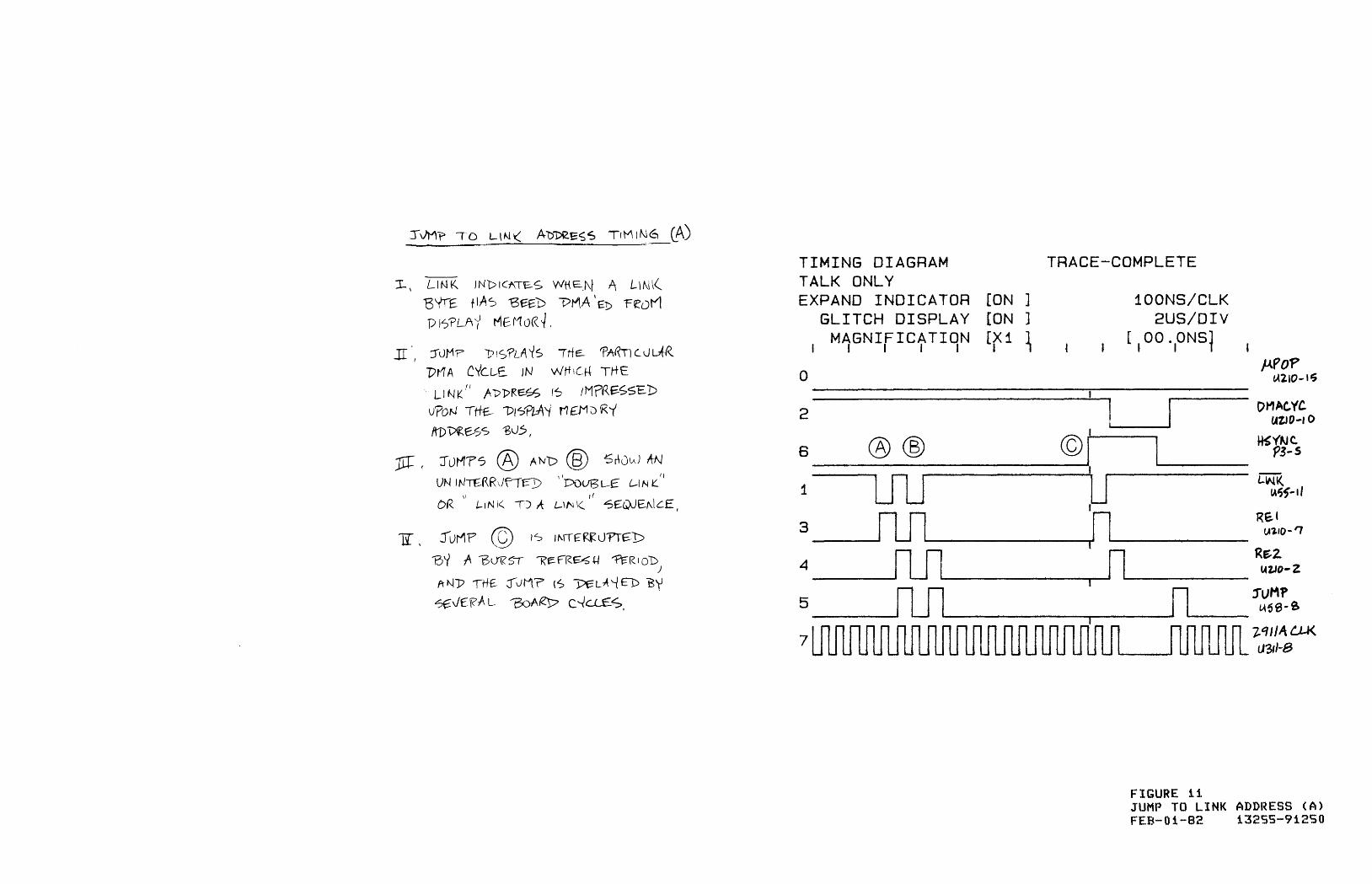
:L, LINK JNDICf\TES WtH=-_I\~ A. L\N~(
"'5YT"£ tlAS 13~£D ""D~A 'ED Feot'! PI~?LA~ M£MoR~,
n I :ruM? l/IS'PLAYS Itf~ 1'AIITlC.0LAR 1)t-1 A CYc.L-E. IN wtt ICH Tt+E
. Ll Nr:. (I ~-P1>RE--9; I~ tM?Re;:$SEj)
V?ON --rtf£-- 1)/s'?L:A"I t1 £Mi) K'-(
1tD~e-.ss 'BJ5,
]If ( TuM?? ® ANt:> ® ~r\0tAJ A-N
'If, JuMP © IS 1{\\T£Rt::uTI~D 'BY It 'BVRST 'K~f"RGo;; i-I ~RI ob
)
AN}) Ttff- j'"JM? (s ~L~'--lf1) "BY ~v£f(A L 'NARt? C..J, C1.£S ,
TIMING DIAGRAM TALK ONLY EXPAND INDICATOR
GLITCH DISPLAY MAGNIFICATION
I I I I
o
2
6 ® ®
TRACE-COMPLETE
I
iOONs/eLK 2US/DIV
[ 00. ONSl I I 1
DMAC.YC lAZJO-IO
P3-S ©I ~y'NC.
--------------------------~
________ ---wJunL-____ - __ ::~-II 1
3
5
7
. _ lA1.10 - '7
I n ..... ______ ~!-z
FIGURE 11.
J'uM' tA~e-S
~qJ/ALU<
Ll3I1-B
JUMP TO LINK ADDRESS (A) FEB-01-B2 13255-91250

r. LINK 1~.r{»)CAT£<; WH~~I A LINI<"
"BYTE t{ At; -g€:. EN 'Dt1 A ~d r R ot'-1 "D1'3?L A ~ M E:f'I\ eX( y.
1[ \ . :rJM? l)(S?LA~S THE ?ARTIC.ULAR.
DI1A (>?c.L-E IN wttlCH THE ... \ I(
LINK A'P1X.E-SS t<':> IM'PR£-SSE1::>
OP0N ,tt£ '!>IS'PLAY M£tActC'i ADl)rRE:.SS ~VS (
--< ~ ® " II III , ..) U, \? IS A t-lD~MA!-)
uN ''''''T~~ lJ'frE1) .::ruM? Sf3&JENCe
1t- I :r0M~ @ IS \N\£~Q.~u""8'-1
A ?KOC~~SDK \)£ lJ\" E I/ ()I' I E
AU-f.SS ANt> 60A K'1:> c ~c..L.J='
I
TIMING DIAGRAM TALK ONLY EXPAND INDICATOR
GLITCH DISPLAY MAGNIFICATION
I I I 1
0
2J 8
1 ~ 3 rTI
,n 4
in 5 I
7
[ON ] [ON ] [Xi • ~
TRACE-COMPLETE
iOONs/eLK 2US/DIV
[ 00. ONsi f I
n )APO~ (A'2.IO .... 'S
I
U DMt\t~ ~2-'O-1 D
I H5,{NC.
1"3 -s I -I®I "I~K.
t.4,&J;S-1( I n R~'
tA.llo-~
n RE.2 U1.10-Z.
rvt1'P n ~ ... 8
1.'111 A C.t,K u'aH·&
FIGURE 12 JUMP TO LINK ADDRESS (B) FEB-01-82 13255-91250

T StiFTC L..K IS ~et-Je'RATE'D WHEi'l E"E'K. ~,
1+ C+\A'R~~ IS "Dt1A ~ not'\. 1)IS'PLA'" MtI'-1o~Y.
11:. ~.\~HIY (~o) 0DES ~\Gt4 Wtt£~ Tt+E 'EI e:-ttitr-TH cI-\ARACTfi< KA5 B'C~tJ rf'L.H£""D,
fir. I E I~ Hl~ Lao) C A USE.'? 1)11\ TO
C~N;t:. ITILL Tftf. /'I'€'Il.T
C-4A-'KALT'€."K 'Row !3£tt l .... IS
TIMING DIAGRAM TALK ONLY EXPAND INDICATOR
GLITCH DISPLAY MAGNIFICATION
I I I I I
o
inn I 2
3
4
5
6
7
[ON] [ON ] C«i ~
TRACE-COMPLETE
50NS/CLK iUS/DIY
[ 00. ONSl I I 1
FIGURE 13
CHAit lA1S-q
INc.u..K 1).38 -II
£''-HTY (liO) <A311-io
(fA-; tftfB -.q
ffi u4&-'7
r>IiAt'/c.. ('(1.'0-'0
END OF EIGHTY CHARACTER LINE FEB-01-82 13255-91250

L. T ~'h ~ T I ~1 I,; (. 1/ i !\C-j;.:}";-i 't j"';> J::UI '1-:, Trf F.:.-
e A s~ "5e ,) F- ,,/ "'? OV-JS 0 F C'N. E F AAME
AAIr;, THE F,«5T 'f.<.OLJ.) DF .t\(\iOTt16R
I. VElAr-HZ l'5 ~€~ESEMTATH/E or- THE. Ve"'R T't cAt... "R t: .RAe. E. l' e'R l o!>
lIT.. £l)'KO-.N M ARK~ TI1£ "'BE ~ \NN lN~ of IH E II N~)(T 1\ 1> A TA RoW
lSL. ® MA''\\(~ A "ROw Dr: C\1A~crER5 DH,t.'~"
fRoM 1),s?LA'(' ~~t10ft'1' foR 1>lS'PLA'" ON
~OW \a. 1[, ~o""-s \q ANt) '20 AKE.. 1St.I\N~ LlNGS
ON Tt+~ ~C~~€N C1<€AT6.J) B'i ED L\~.
2I. 'ROW'5 21) 2 2 , Z3 f\'K'E 'B L4N ~ ON
THE. St~6E'N As A "K~t5vL..\ DF AN c!:OP. ---"$[. A lOW ~TA-T€- DN st6NAL t;{~I'f'~ (80)
lNT)( (A: T~S T~A-r l),..,A of( 'BLANl('
ftL-L IS A-Lr\YE. J\ tf((~ H ~TAlE.. \NO Ic..ATES T ~AT TH E. "DY\A IS II "
OFF DR ,NA(", '\1£.
~ @ !-'lAR\(? "Dt'I A f"o1( 'Row 2-4 .) Wtrl,-ij
"PO~~N:.r ~)(l-51 AN'P loS N~v&R 1>~~LA"'IS"D,
TIMING DIAGRAM TALK ONL¥ EXPAND INDICATOR
GLITCH, DISPLAY MAGNIFICATION
I I I' I I
5
El I I o f® I 11 I 2 I I 3
4
• I 1
I ~ I I I I
~ .~ I'?
[ON] [ON]
[r 1 ~
I
~ 2.0
TRACE-COMPLETE
~ "2..1 "22
25US/CLK 500US/DIV
[ 100 -IONS1
I I C I I I
I I
Y13LAN 'K ?;-:f
~D'ROVV
P?, -IS
£OL uss - iO
'1:.01../ V(,I\O - \ D
f.N'D £01 .. : oft z..vc:' lAlIO - /"j
LoP u'5:S -9
@) I W-pl
tA,1I0-'2..
~ ~ U £!6lfr Y ( eD) t'(3)1-~
'i. z.3 "R~'AALf: 0
FIGUI~E 14 END OF LINE AND END OF PAGE FEB- 0 1-B~? 132S~j-912S0

t)KI~ ~o - DF- LINE TI M ,,aJ4
:r Tths 'D(A-6~M. b\SPL1\"~ ~ TY'PlutL
TlM.fNf1 S€Qv€tJCE FO"e ~ 5K.'P
~t> ... o'F ... (,l NE. ~·fV'T'~'
1[., ?tUPfWL.- (-S cS e;.IJ ~~ 13'(' TH-E bt4t It -srItTt M~c:ri-f~E J G, VE.N TfiE 'fR an=:.~
~~f\\TS oc..C&l~,
1!L\ \AtaIO-<t I, ,;r\M{'(...&.b -S'? £'O'R. AN'!)
e.AVS';"~ SK\P£t)(...' To SW~ -5rA-~.
EAC-H L.\N~ ~~vW~E. STlWB£S w,.O TO A-rr~"'PT ~C> ~.P T~ :SKtffOt,,' ~oDE. If' H~'('- L.-(Ale. ~'NTEi.. F~ t$ l-h~ft,
i~ I,\N \(. 'PO'NTS lb "'D1f11t O~ TtfE.
~~t:: c..tfAAAcr~ RD\\J kt-J]> ~\<\PE,Dt,' ~~ ,; NO-r ~~INAT"6l>,® If N ~r l,1~e... ?ot'" n:;R t:L..~ 'S Low,
iH-~ L.IN~ ?Ol"'lS TO ~A ON. tt+~ N~1""" t+\AAAc.:~ 'ROw /tffJ> 5KlProL.J tIlO"C>~ I" n;RMIN~~ . @
TIMING DIAGRAM TALK ONLY EXPAND INDICATOR
GLITCH DISPLAY MAGNIFICATION
I I I I
0 I 1 I 2
3
4
5
6
7
[ON] [OFF]
(~1 ~
TRACE-COMPLETE
I
500NS/CLK 10US/DIV
[ tOO -.ONSi ~'?£OL lA"O-'~
UiliO -'I
f.'DR. u'5{, -l.
-S\('(~L.' tAI,,'O-5
f
J NaT t.:.1"'£ ft)(Hnut 'RA~
UIo5-~
~ ~ ~~2-~z..o-2..
@ wt.! (.A 110 -tb
I
U ~ liiC U5S-1 \
FIGURE 1S SKIP END OF LINE FEB-01-82 13255-91250

XU11 n c101t--__ ----t , '22;;24~===~ L~4UJ .. ___ ..... XU21
~ C7W
XU3l
C8 I XU4l
C12 lL I
XU5l j C13
m 1 XU6l
C15
U12
R1
U22
r- Rll
U32
U42
I U52
R15 CRl
C19 ill ..... 1 _X_U7_1 --41 0 N ~ 01 XU81 1 W2 0 0
Wl
C2
U23
q U33 ~I U34 5 I R121 I I IR13
~ I U43 ~ I U44 9 R161 I I IR17
q U53 q U54 q R18 R191
,.... C") ~ C\I C\I o 0
U25
U35
U45
U55
U65
R3 R5 R6 R7
ITIJ" SW1m U19
R4
r---------t t--__ ---,R9r--__ --.C3 ___ --' --------'50 I Ull1 [tJ
51 U26 51 U27 5 I U28 51 U29 '--__ -J-', ___ ~5 I U2l1 50
C9 R14 Rl0
5 U36 SOl U37 ___ U_38_-J5 ..... 1 _U3_9_...J 501 '---_----1501 L-_U_3l_l ----IsD
51 5 c::J1 U46
Cl0 Cll
U48 5 L-I _U4_9_...J ""'1 ___ ~5 .... 1_u_4l_l_ ...... s I I
U5l0 5 1,-_u_5_l1_~5 C18
C27 0
__ --...... C_17 ,.....-__ ....,
U57 5 I U58 CO 1 U59 5 I ,--U_5_6 ----IS I
U66 5 ~I U68 5 I
C26
C(] I'--_--J C25
___ U_69_....J5 ..... 1 _U6_l_0 _CIl ____ u_6l_l_...J5
R25
,--_U_79 __ {fl~U_7_l0_~~U_7_ll_~cO I U78 COl R20 R2l R22 R23 R24
FIGURE 16 COMPONENT LOCATION DIAGRAM FEB-01-B2 13255-91250

Reference Designation
Cl C~~ C3 C4 C5
C6 C7 CEl C9 C10
Cl1 C12 C13 C14 C15
C16 C17 Ct8 Cl '}>
C~'.O
C;'.1 C;.:~2
C23 C:''.4 C25
C:''.6 C27
CI~ 1 CR2 CIU
Rl R:,:'. R:3 R4 R5
R6 R'7 Rfl R9 R10
R11 R12 R13 R'14 R15
Rt6 RHI R19 R;:~O
R :,:'.1
SWI
U11 U'12 U19 U:''.l LJ22
U;:'.3 LJ24 U:''.5 LJ26 U:''.7
LJ28 U~->'9
U31 U:32 U33
HP Part Number
c o
02640-60250 2
0160-4554 0'160-4554 0160-4554 o '1 60-'4~;j57 0160,,,4557
o 1 60-o4~:i54 0160,-4557 o 160'-o4~:i57 0160--4557 o '160"-4~)54
0160-4~)54
o 160-'4~)57 0160-4557 0'160-o4:':i54 0160--4:7i57
II '1 60'-'4~'i57 o 160--4:':'i54 IJ '1. 60-o4~:i54
0160-4:':'i57 (J 1 60-o4~:i57
01 BO-2B'79 0180-,,2079 O'lBO-2f.l79 IJ 1 80-"2f:l79 0160-04554
0160-o4::i57 0'160-4554
1'tOl-'0050 1';>01-'0050 'I 'l 02-'30'n
IBI0-"0:~22 HI 1 0 .. ·0;:'.79 1l6B~3-'1 03~i IH,83-1035 06B~~-'1 035
(}6B3-47~,!5
06133--4725 11683-,,4715 [)MI3-10;?:':'i 1l6!33-A7:.?5
lBl 0-"0~322 H1I0-'O:522 11310-0;'.79 11683-,4715 W10-0322
:I 1'110-,0;:'.79 1J6B3'''471::i HII0-'O~'.05
06B3-'-4n~5
0683--4'725
06f.l3--1035 06B3-4725 0613:'5-4725 0683-04'725 HI1 O'-0~322
~11 01-2063
'IB18-1397 1. 1'120-,2523 :lB16-14B6 ') 1'118-1:597 "[f.l20-2523
1.820-,2523 11820,-1453 lE120-1730 :l8;~0-1196 1820-0629
1,820-1449 11:116-,,1485 1818-1397 If:120-2024 18;:,'0-2523
7 7 7 o o
7 o o o 7
7 o o 7 o
o 7 7 o o
7 7 7 7 7
o 7
3 3 1
9 5
''J 2
9 9 5 o 9
5 o 7
2
2 9
8
6 7 o 6 7
7 o 6 8 o
4 9 6 3 7
Qty
11
12
4
3 4
:3 1
8 4 1
2
4
Replaceable Parts
Description
DISPLAY MEMORY/DMA PCA DATE CODE: A-2218-42
CAPACITOR-FXO .0IUF +-20% 50VOC CER CAPACITOR-FXD .0IUF +-20% 50VDC CER CAPACITOR-FXO .0IUF +-20% 50VDC CER CAPACITOR-FXD .1UF +-20% 50VDC CER CAPACITOR-FXO .1UF +-20% 50VDC CER
CAPACITOR-FXD .01UF +-20% 50VDC CER CAPACITOR-FXO .1UF +-20% 50VDC CER CAPACITOR-FXD .IUF +-20% 50VDC CER CAPACITOR-FXD .IUF +-20% 50VDC CER CAPACITOR-FXD .01UF +-20% 50VDC CER
CAPACITOR-FXD .01LJF +-20% 50VDC CER CAPACITOR-FXD .1UF +-20% 50VDC CER CAPACITOR-FXO .1UF +-20% 50VOC CER CAPACITOR-FXD .01UF +-20% 50VDC CER CAPACI10R-FXD .1UF +-20% SOVDC CER
CAPACITOR-FXD .1UF +-20% 50VDC CER CAPACITOR-FXD .OIUF +-20% 50VDC CER CAPACITOR-FXD .01UF +-20% 50VDC CER CAPACITOR-FXO .1UF +-20% SOVDC CER CAPACITOR-FXD .1UF +-20% 50VDC CER
CAPACITOR-FXO 22UF+50-10% 25VOC AL CAPACITOR-FXD 22UF+50-10% 25VDC Al CAPACtTOR-FXD 22UF+50-10% 25VDC AL CAPACITOR-FXD 22UF+50-10% 25VDC AL CAPACITOR-FXO .01UF +-20% 50VOC CER
CAPACITOR-FXD .1UF +-20% 50VDC CER CAPACITOR-FXD .OlUF +-20% SOVDC CER
DIODE-SWITCHING SOV 200MA 2NS DO-35 DIODE-SWITCHING SOV 200MA 2NS DO-35 DIODE-INR 4.99V 2% DO-35 PD=.4W
NETWOR~-RES 8-SIP20.0 OHM X 4 NETWOR~-RES 10-SIP4.7K OHM X 9 RESISTOR 10K 5% .25W FC TC=-400/+700 RESISTOR 10K 5% .25W FC TC=-400/+700 RESISTOR 10K 5% .25W FC TC=-400/+700
RESISTOR 4.7K 5% .25W FC TC=-400/+700 RESISTOR 4.7K 5% .25W FC TC=-400/+700 RESISTOR 470 5% .25W FC TC=-400/+600 RESISTOR 1K 5% .25W FC TC=-400/+600 RESISTOR 4.7K 5% .25W FC TC=-400/+700
NETWORK-RES 8-SIP20.0 OHM X 4 NETWORK-RES 8-SIP20.0 OHM X 4 NETWORK-RES 10"SIP4.7K OHM X 9 RESISTOR 470 5% .25W FC TC=-400/+600 NETWORK-RES 8-SIP20.0 OHM X 4
NETWORK-RES 1 O'-SIP4. 7K OHM X 9 RESISTOR 470 S% .25W FC TC=-400/+600 NETWORK-RES 8-SIP4.7K OHM X 7 RESISTOR 4.7K 5% .25W FC TC=-400/+700 RESISTOR 4.7K 5% .25W FC TC=-400/+700
RESISTOR 10K 5% .25W FC TC=-400/+700 RESISTOR 4.7K 5% .25W FC TC=-400/+700 RESISTOR 4.7K 5% .25W FC TC=-400/+700 RESISTOR 4.7K 5% .25W FC TC=-400/+700 NETWORK-RES 8-SIP20.0 OHM X 4
SWITCH-RKR DIP-RKR-ASSY 4-1A .05A 30VDC
IC-RAM 16K (PLAST) IC-;:'911A IC-ROM 256 X 4 HM7611 IC-RAM 16K (PLAST) lC"'2911 A
IC-2911A IC CNTR TTL S BIN SYNCHRO POS-EDGE-TRIG IC FF TTL lS D-TVPE POS-EDGE-TRIG COM IC FF TTL LS O-TVPE POS-EOGE-TRIG COM IC FF TTL S J-K NEG-EDGE-TRIG
IC GATE TTL S OR QUAD 2-INP IC-ROM 256 X 4 HM7611 IC"-RAM 16K (PLAST) IC DRVR TTL LS LINE DRVR DeTl IC-;:~911 A
Mfr Code
284130
28480 213480 (:'8490 16299 16299
28480 16299 16299 16;~99
28480
213480 16299 16299 ~~f.1480
1629';'>
16299 ::?848 0 2B480 16299 16299
213480 2B400 28480 20480 ?B480
16299 ;:'.8480
28480 213480 2f:l480
01 H'l 0'1121 01121 01121 01t?1
0'1121 011 ?1 01.121 0011 ?1 0'1121
011 ::'.1 01121 01121 0'1121 o 11 ~'.1
01t21 011 ;':>1 Ot121 01121 01.121
0'1121 011?1 01 1::.' 1 01121 o 11 ~~ 1
20480
80545 28480 34371 S054~5 284f.IO
284ElO 01295 01295 01295 01295
01295 343'71 S0545 01295 213480
Mfr Part Number
02640-602S0
0160-4~i54
0160-4554 o 160-4~,'i54 CAC04X7R104M050A CAC04X7RI04M050A
0160,-4554 CAC04X7R104M050A CAC04X7RI04M050A CAC04X7RI04M050A 0160-4554
0160-4::-;54 CAC04X7RI04M050A CAC04X7RI04M050A 0160,-4554 CAC04X7Rl04M050A
CAC04X7R104M050A 0160-4554 0160-4554 CAC04X7R104M050A CAC04X7Rl04M050A
o t BO-287')> 0180-2879 0180-2879 0100,-2879 o 160-4::,iS4
CAC04X7RI04M050A () 16 0-4:")54
1901-0050 1901-0050 1 ~)02-3092
408F.1200J 210A472 CBl 0 :'35 CB1035 CBI0:35
CB4725 CB47::~5 CB4715 CBI025 CB47;~5
408B20 OJ 408B200J 210A4'n CB4715 408B200J
210A472 C1I4715 200A472 CB4n~5
CFc4725
CBI0:35 CB4725 CB47?5 CFc4725 408B200J
3101-2063
UP416C-3(SELECTED) 1820,,-2523 HM3-7611A-5 PROGRAMMED UP4t6C-3(SELECTED) 1820,,2523
1820"-2523 SN74St63N SN74LS273N SN74LS174N SN74St12N
SN74S32N HM3-7611A-5 PROGRAMMED UP416C-3(SELECTED) SN74LS244N 18::?,0-25;':~3

Reference Designation
U34 U35 U36 U~!l7
1I38
U:!l9 U41 U42 U43 1.144
U45 1.146 U47 1.148 LJ49
U~:i1 U52 U~:;3
U54 U~:;5
U56 U~:;7
U58 U~;9
U59
Ul:>l UbS U66 U67 U68
U71 U'78 U79 UBI UI10
U 111 U210 U;:~11
U310 U~!I11
U410 U411 U510 U~;11
U610
U611 U710 U'711
W1 W;.:~
XU11 X1.l21 XU31 XU41 XU51
XU61 XU71 X1.l81
HP Part Number
1820-0683 1 B20-·1989 1820-0686 H120-0681 1820····1433
HI20-1;;?'Ol 1818-1397 18:.=.!0-1438 18;~O-14:38
1E1;.~0-·21 02
1820-1730 1020-,1199 1B13--02?Fl 1820-,1440 1£120-0693
1£1"18-13<;17 18,~0-2024
18;.~0-20;;?'4
1820--2024 1816-·1404
1820-120B 1£:120-.. 1112 1820-11"12 H120-1 "112 tf.l;~0--120B
H118-1397 11320-'190~j
1f:120-1202 1820-1206 1820-1 ;:~01
1818·-1:397 HI20-·1199 18;~0-1201
1f:118-1397 1820-1076
1B::?0-1144 1820-1191 H120-0691 1820--1322 1f:120-·1 :567
18;~0-1197
H120-Hl7b 1820--1208 11320-1876 1820-1112
113;.=.!0-1212 1820'-1209 1820-,,1112
B159-000~;
8"159-0005
1200-0853 1;:~00-0853 1200-08::n 1~~00-01353 1200-08~j3
1200-0853 120 0-08~j:3 1200 -- 08~j3
0360-16El2 0"150-2333
c o
6 7 9 4 6
6 6 1 1 8
6 1 o 5 8
6 3 3 3 8
3 8 8 8 3
6 7 7 1 6
6 1 6 6 :5
6 3 6 2 5
9 1 3 1 8
9 4 8
o o
8 8 8 8 8
8 8 8
o 3
Qty
3
2
5
2
8
6
Table 6·3. Replaceable Parts
Description
IC INV TTL S HEX 1-INP IC CNTR TTl.. lS BIN DUAL 4····BIT IC GATE TTL SAND TPL 3-INP IC GATE TTL S NAND QUAD 2-INP IC SHF· .. RGTR TTL U3 R-S SERIAL·-IN PRI..···OUT
IC GATE TTL LS AND QUAD 2-INP IC····RAM 16K (PL.AST> IC MUXR/DATA-SEl TTL lS 2-TO-1-LINE QUAD Ie MUXR/DATA-SEL TTL LS 2-TO-1-LINE QUAD Ie LCH TTL LS D-TVPE DCTl
IC FF TTL LS D-TVPE POS-EDGE-TRIG COM IC INV TTl.. LS HEX 1-INP OSCILl..ATOR- 21 ,34MHZ IC LCH TTL l..S QUAD IC FF TTL S D-TVPE POS-EDGE-TRIG
IC-RAM 16K (PLAST) Ie DRVR TTL LS LINE DRVR nCTL IC DRVR TTL l..S LINE DRVR DCTL IC DRVR TTl.. LS LINE DRVR DCTl.. IC-ROM 256 X 4 HM7611
IC GATE TTL LS OR QUAD 2-1NP IC FF TTL LS D-TVPE POS-EDGE-TRIG IC FF TTL LS D-TVPE POS-EDGE-TRIG IC FF TTl.. LS D-TVPE POS-EDGE-TRIG IC GATE TTL l..S OR QUAD 2-INP
IC-RAM 16K (PLAST) IC GATE TTl.. LS NOR DUAL 5-INP IC GATE TTL LS NAND TPL 3-INP Ie GATE TTL l..S NOR TPL 3-INP IC GATE TTL LS AND QUAD 2-INP
lC"-RAM 16K (Pl..AST) IC INV TTl.. LS HEX l-INP Ie GATE TTL LS AND QUAD 2-INP IC-RAM 16K (PLAST) IC FF TTL S D-TVPE POS-EDGE-TRIG CLEAR
IC GATE TTL LS NOR QUAD 2-INP IC FF TTL S D-TVPE POS-EDGE-TRIG COM IC GATE TTL S AND-DR-INV IC GATE TTL S NOR QUAD 2-INP IC GATE TTL S AND QUAI> 2····INP
IC GATE TTL LS NAND QUAD 2-INP IC CNTR TTL S BIN SVNCHRO POS-EDGE-TRIG IC GATE TTL LS OR QUAD 2-INP IC CNTR TTl.. S BIN SVNCHRO PDS-EDGE-TRIG IC FF TTL LS D···TYPE POS·_·EDGE-··TRIG
IC FF TTL LS J-K NEG-EDGE-TRIG lC eFR TTL LS NAND QUAD 2-INP IC FF TTL LS D-TVPE POS-EDGE-TRIG
RESISTOR-ZERO OHMS 22 AWG LEAD DIA RESISTOR-ZERO OHMS 22 AWG l..EAD DIA
SOCKET-IC 16-CONT DIP DIP-SLDR SOCKET-IC 16-CONT DIP DIP-SLDR SOCKET-IC 16-CONT DIP DIP-SLDR SOCKET-IC 16-CONT DIP DIP-SLDR SOCKET-IC 16-CONT DIP DIP-SLDR
SOCKET-IC 16-CONT DIP DIP-SLDR SOCKET-IC 16-CONT DIP DIP-SLDR SOCKET-IC 16-CDNT DIP DIP-SLDR
TERMINAL-STUD BGl-TUR PRESS-MTG WIRE 30AWG W 42V TEFZ8_ lX30 105C
Mfr Code
01295 07263 01295 01295 () 1 ;?'9~i
01295 80545 o 1;l95 01;:>95 012<;>~,)
01295 01;:><75 ;?0480 0129~.'i
O"\29~;
SO~j4~:;
o 1 ;:.~9~:.'i o 1 ;~95 O"l ;:~95 34:~71
o 1 ;:.~95 012<75 01295 III ;~95 0129:7i
SO~:;4~:;
07263 01295 012n5 01295
~:;0545
ll1:,'95 01295 S054~:;
01 ;?95
01295 o 129~j 012<;>5 012<75 01295
O:l295 :~43~~5 0129:7; 34:B5 01295
01295 01295 01295
28480 2t=l480
28480 ;:~B4130 28480 ;:~f1480 ;:~134BO
2n480 20480 20480
28480 2f.l480
Mfr Part Number
SN74S()4N 74L.S~393PC SN74S11 N SN74800N SN74LS164N
SN74LSOflN UP416C-3(SEl..ECTED) SN74LS2~;7AN
SN74L.S257AN SN74LS3T~N
SN74LS;:'.T3N SN'74LS04N 1 I'll :~-O;:>;.:.'1:1 ~3 N7 41. ~3279N r"N74S74N
UP416C-3(SFlECTED) SN74U3244N SN'741.S244N SN'741..S244N HM3-7611A-5 PROGRAMMED
SN'74LS32N SN74l.S74AN SN74LS74AN BN74lS74AN SN74LS3t.'N
UP416C-3(8FLECTED) 74ln;:'60PC SN74LSI0N nN74LS27N SN74LSOflN
UP41hC-3(SELECTFD) SN'74LS04N SN74LS013N l.lP416C-3(SELFCTED) nN74S174N
BN74LSO;?N BN74S1'7:7jN SN74S64N SN74S0?N SN74S08N
f:lN74LSO ON AM74S161N nN74LS3;:'N AM74B161N SN74LS74AN
SN74LS112AN SN74LS3BN SN74LS74AN
8"l59-0005 8159"·0005
1200-0853 1200',-0853 1200-0853 1200-0853 1::>00-0853
1200-0853 1200-0853 1200-0853
0360-1682 8150·_·2333
M ANUFACT U R E R S COD E LIS T AS OF 06/21/82 PAGE
MFR ZIP NO. MANUFACTURER NAME ADDRESS CODE
5054:5 NIPPON ELECTRIC CO TOKYO JP 00000 ANY SATISFACTORY SUPPLIER 01121 ALLEN-BRADLEY CO MILWAUKEE WI 53204 01295 TEXAS INSTR INC SEMICOND CMPNT DIV DALLAS TX 75222 04713 MOTOROLA SEMICONDUCTOR PRODUCTS PHOENIX AZ 85008 01263 FAIRCHILD SEMICONDUCTOR DIV MOUNTAIN VIEW CA 94042 16299 CORNING GLASS WKS COMPONENT DIV RALEIGH Ne 27604 28480 HEWLETT-PACKARD CO CORPORATE HQ PALO ALTO CA 94304 34335 ADVANCED MICRO DEVICES INC SUNNYVALE CA 94086 3437t HARRIS SEMI CON DIV HARRIS-INTERTYPE MELBOURNE FL 32901 50088 MOSTEK CORP CARROL.LTON TX 75006