datasheet for telink ble soc tlsr8266/ tlsr8266f512 · 2018-04-13 · datasheet for telink...
TRANSCRIPT
Datasheet for Telink
BLE SoC TLSR8266/
TLSR8266F512
DS-TLSR8266/TLSR8266F512-E19
Ver 2.0.2
2015/06/02
TE
LIN
KS
EM
IC
ON
DU
CT
OR
Keyword:
Features; Package; Pin layout; Working mode;
Memory; MCU; RF Transceiver; Baseband; Clock;
Timers; Interrupt; Interface; PWM; KeyScan; Audio;
QDEC; ADC; PGA; Electrical specification; Application
Brief:
This datasheet is dedicated for Telink BLE SoC TLSR8266
(without internal flash) / TLSR8266F512 (with internal
flash). In this datasheet, key features, working mode,
main modules, electrical specification and application of
the TLSR8266/TLSR8266F512 are introduced.
Telink for customer

Datasheet for Telink TLSR8266/TLSR8266F512
DS-TLSR8266/TLSR8266F512-E19 1 Ver2.0.2
Published by Telink Semiconductor Bldg 3, 1500 Zuchongzhi Rd, Zhangjiang Hi-Tech Park, Shanghai, China © Telink Semiconductor All Right Reserved
Legal Disclaimer
Telink Semiconductor reserves the right to make changes without further notice to
any products herein to improve reliability, function or design. Telink Semiconductor
disclaims any and all liability for any errors, inaccuracies or incompleteness contained
herein or in any other disclosure relating to any product.
Telink Semiconductor does not assume any liability arising out of the application or
use of any product or circuit described herein; neither does it convey any license
under its patent rights, nor the rights of others
The products shown herein are not designed for use in medical, life-saving, or
life-sustaining applications. Customers using or selling Telink Semiconductor products
not expressly indicated for use in such applications do so entirely at their own risk and
agree to fully indemnify Telink Semiconductor for any damages arising or resulting
from such use or sale.
Information:
For further information on the technology, product and business term, please contact
Telink Semiconductor Company (www.telink-semi.com).
For sales or technical support, please send email to the address of:
Telink for customer

Datasheet for Telink TLSR8266/TLSR8266F512
DS-TLSR8266/TLSR8266F512-E19 2 Ver2.0.2
Revision History
Version Major Changes Date Author
0.8 Preliminary release 2014/3 Cynthia
1.0
Mainly added section 11~13, and updated
section 1, 7, 10, 14.
Added TLSR8266ET48 package.
2014/5 Cynthia
1.01 Updated section 14.4 2014/5 Cynthia
1.1 Updated section 15 2014/5 Cynthia
1.2 Mainly updated section 1 and section 15 2014/7 Cynthia
1.3 Updated section 4 2014/7 Cynthia
1.4 Mainly updated section 1, section 6 and
section 15 2014/8 Cynthia
1.41 Updated section 14.3 2014/8 Cynthia
1.42 Updated section 1 and section 3 2014/8 Cynthia
1.5 Updated section 8 2014/10 Cynthia
1.6 Added section 2.5, updated section 7.1 and 7.3 2015/1 S.G.J., Cynthia
1.7 Updated section 2.3 2015/1 S.G.J., Cynthia
1.71 Updated section 14.4 2015/3 Cynthia
1.8 Updated section 2.5, 4.4.2, 5, 7.1.3, 7.4, 12 and
14.4 2015/3 Cynthia
1.9 Updated section 1 and 14.2 2015/3 Cynthia
1.91 Updated section 12.5~12.6 and 12.9 2015/4 Cynthia
2.0 Updated section 1.6 and 7.1 2015/4 S.G.J., Cynthia
2.01 Mainly updated section 1.6, 7.1.1.2 and 12.3
Modified Figure 13-1 2015/5 L.L.J., Cynthia
2.0.2 Updated package dimension figures (Figure
1-2~1-4 in section 1.5) 2015/6 X.S.J., Cynthia Te
link for customer

Datasheet for Telink TLSR8266/TLSR8266F512
DS-TLSR8266/TLSR8266F512-E19 3 Ver2.0.2
1 Table of contents
1 Overview ............................................................................................................... 10
1.1 Block diagram .............................................................................................. 10
1.2 Key features ................................................................................................. 11
1.2.1 General features ..................................................................................... 11
1.2.2 RF Features ............................................................................................. 12
1.2.3 Features of power management module ............................................... 12
1.3 Typical applications ...................................................................................... 12
1.4 Ordering information ................................................................................... 13
1.5 Package ........................................................................................................ 15
1.6 Pin layout ..................................................................................................... 19
1.7 Telink SDK .................................................................................................... 32
2 Memory and MCU ................................................................................................ 33
2.1 Memory ....................................................................................................... 33
2.2 MCU ............................................................................................................. 34
2.3 Working modes ............................................................................................ 34
2.3.1 Active mode ............................................................................................ 34
2.3.2 Idle mode ................................................................................................ 34
2.3.3 Power-saving mode ................................................................................ 35
2.4 Reset, Wakeup and Power down enabling .................................................... 35
2.5 Wakeup sources ............................................................................................. 37
2.5.1 Wakeup source - USB.............................................................................. 37
2.5.2 Wakeup source – 32K timer ................................................................... 37
2.5.3 Wakeup source – pad ............................................................................. 37
3 2.4G RF Transceiver .............................................................................................. 39
3.1 Block diagrams ............................................................................................. 39
3.2 Function description .................................................................................... 39
3.2.1 Turn on/off .............................................................................................. 39
3.2.2 Air interface data rate and RF channel frequency .................................. 39
3.3 Baseband ..................................................................................................... 40
3.3.1 Packet format ......................................................................................... 40
3.3.2 RSSI.......................................................................................................... 40
4 Clock ..................................................................................................................... 41
Telink for customer
Datasheet for Telink TLSR8266/TLSR8266F512
DS-TLSR8266/TLSR8266F512-E19 4 Ver2.0.2
4.1 Clock sources ............................................................................................... 41
4.2 Register table ............................................................................................... 41
4.3 System clock ................................................................................................ 43
4.4 Module clock ................................................................................................ 44
4.4.1 ADC clock ................................................................................................ 44
4.4.2 DMIC clock .............................................................................................. 44
5 Timers ................................................................................................................... 46
5.1 Timer0~Timer2 ............................................................................................ 46
5.1.1 Register table .......................................................................................... 46
5.1.2 Mode0 (System Clock Mode) .................................................................. 48
5.1.3 Mode1 (GPIO Trigger Mode) .................................................................. 48
5.1.4 Mode2 (GPIO Pulse Width Mode) .......................................................... 49
5.1.5 Mode3 (Tick Mode) ................................................................................ 50
5.1.6 Watchdog ................................................................................................ 51
5.2 32K LTIMER .................................................................................................. 52
5.3 System Timer ............................................................................................... 52
6 Interrupt System ................................................................................................... 53
6.1 Interrupt structure ....................................................................................... 53
6.2 Register configuration ................................................................................. 53
6.2.1 Enable/Mask interrupt sources .............................................................. 54
6.2.2 Interrupt mode and priority ................................................................... 54
6.2.3 Interrupt source flag ............................................................................... 55
7 Interface ............................................................................................................... 56
7.1 GPIO ............................................................................................................. 56
7.1.1 Basic configuration ................................................................................. 56
7.1.1.1 Multiplexed functions ........................................................................ 56
7.1.1.2 Drive strength .................................................................................... 57
7.1.1.3 GPIO lookup table .............................................................................. 57
7.1.2 Connection relationship between GPIO and related modules ............... 61
7.1.3 Pull-up/Pull-down resistor ...................................................................... 64
7.2 SWM and SWS ............................................................................................. 70
7.3 I2C ................................................................................................................ 70
7.3.1 Communication protocol ........................................................................ 70
7.3.2 Register table .......................................................................................... 71
Telink for customer
Datasheet for Telink TLSR8266/TLSR8266F512
DS-TLSR8266/TLSR8266F512-E19 5 Ver2.0.2
7.3.3 I2C Slave mode........................................................................................ 72
7.3.3.1 DMA mode......................................................................................... 73
7.3.3.2 Mapping mode .................................................................................. 74
7.3.4 I2C Master mode .................................................................................... 74
7.3.4.1 I2C Master Write transfer ...................................................................... 75
7.3.4.2 I2C Master Read transfer ....................................................................... 75
7.4 SPI ................................................................................................................ 76
7.4.1 Register table ............................................................................................... 76
7.4.2 SPI Master mode ......................................................................................... 77
7.4.3 SPI Slave mode ............................................................................................ 78
7.5 UART ............................................................................................................ 79
8 PWM ..................................................................................................................... 83
8.1 Register table ............................................................................................... 83
8.2 Enable PWM ................................................................................................ 86
8.3 Set PWM clock ............................................................................................. 86
8.4 PWM waveform, polarity and output inversion .......................................... 86
8.4.1 PWM waveform ...................................................................................... 86
8.4.2 Invert PWM output ................................................................................. 87
8.4.3 Polarity for signal frame ......................................................................... 87
8.5 PWM mode .................................................................................................. 88
8.5.1 Select PWM mode .................................................................................. 88
8.5.2 Continuous mode ................................................................................... 88
8.5.3 Counting mode ....................................................................................... 88
8.5.4 IR mode ................................................................................................... 89
8.6 PWM interrupt ............................................................................................. 90
9 Keyscan ................................................................................................................. 91
9.1 Register table ............................................................................................... 91
9.2 Keyscan enable ............................................................................................ 95
9.3 Keyscan IO configuration ............................................................................. 96
9.4 Keyscan flow and frame ............................................................................... 97
9.5 Keyscan FIFO buffer ..................................................................................... 99
10 Audio .................................................................................................................. 100
10.1 Audio input path .......................................................................................... 100
10.2 Audio input processing ................................................................................ 100
10.3 Audio output path ....................................................................................... 102
Telink for customer

Datasheet for Telink TLSR8266/TLSR8266F512
DS-TLSR8266/TLSR8266F512-E19 6 Ver2.0.2
10.3.1 Rate Matching ......................................................................................... 102
10.3.2 SDM ....................................................................................................... 103
10.3.3 Register configuration ........................................................................ 104
10.4 Audio performance ...................................................................................... 105
11 Quadrature Decoder .......................................................................................... 107
11.1 Input pin selection ....................................................................................... 107
11.2 Common mode and double accuracy mode................................................ 108
11.3 QDEC interrupt............................................................................................. 110
11.4 QDEC reset ................................................................................................... 110
11.5 Other configuration ..................................................................................... 110
11.6 Register table ............................................................................................... 111
12 ADC ..................................................................................................................... 113
12.1 ADC clock ..................................................................................................... 113
12.2 Set period ..................................................................................................... 113
12.3 Select ADC input range ................................................................................ 114
12.4 Select resolution and sampling time ........................................................... 114
12.5 Select input mode and channel ................................................................... 114
12.6 Enable auto mode and output ..................................................................... 115
12.7 ADC done signal ........................................................................................... 115
12.8 ADC status .................................................................................................... 115
12.9 Register table ............................................................................................... 116
13 PGA ..................................................................................................................... 119
13.1 Left/Right channel enabling ......................................................................... 119
13.2 Input channel selection ............................................................................... 119
13.3 Gain setting .................................................................................................. 119
13.4 PGA output .................................................................................................. 120
13.5 Register table ............................................................................................... 120
14 Key Electrical Specifications ............................................................................... 123
14.1 Absolute maximum ratings .......................................................................... 123
14.2 Recommended operating condition ............................................................ 123
14.3 DC characteristics ........................................................................................ 124
14.4 AC characteristics ......................................................................................... 124
15 Applications ........................................................................................................ 128
15.1 Application example for the TLSR8266ET48 ................................................ 128
15.1.1 Schematic .............................................................................................. 128
15.1.2 Layout ................................................................................................... 130
15.1.3 BOM (Bill of Material) ........................................................................... 131
Telink for customer

Datasheet for Telink TLSR8266/TLSR8266F512
DS-TLSR8266/TLSR8266F512-E19 7 Ver2.0.2
2 Table of Figures
Figure 1- 1 Block diagram of the system .............................................................. 10
Figure 1- 2 Package dimension for the TLSR8266ET/AT56 (Unit: mm) ................ 16
Figure 1- 3 Package dimension for the TLSR8266ET/AT48/TLSR8266F512ET/AT48
17
Figure 1- 4 Package dimension for the TLSR8266ET/AT32/ TLSR8266F512ET/AT32
19
Figure 1- 5 Pin assignment for the TLSR8266ET/AT56 ......................................... 19
Figure 1- 6 Pin assignment for the TLSR8266ET/AT48 ......................................... 22
Figure 1- 7 Pin assignment for the TLSR8266ET/AT32 ......................................... 25
Figure 1- 8 Pin assignment for the TLSR8266F512ET/AT48 ................................. 27
Figure 1- 9 Pin assignment for the TLSR8266F512ET/AT32 ................................. 30
Figure 2- 1 Physical memory map ....................................................................... 33
Figure 2- 2 MCU memory map ............................................................................ 33
Figure 2- 3 Transition chart of working modes .................................................... 34
Figure 2- 4 Wakeup sources ............................................................................... 37
Figure 3- 1 Block diagram of RF transceiver ........................................................ 39
Figure 4- 1 Block diagram of system clock ........................................................... 43
Figure 7- 1 Logic relationship between GPIO and related modules .................... 61
Figure 7- 2 I2C timing chart ................................................................................. 70
Figure 7- 3 Byte consisted of slave address and R/W flag bit .............................. 72
Figure 7- 4 Read format in DMA mode ................................................................ 73
Figure 7- 5 Write format in DMA mode .............................................................. 73
Figure 7- 6 Read format in Mapping mode.......................................................... 74
Figure 7- 7 Write format in Mapping mode ......................................................... 74
Figure 7- 8 SPI write/read command format ....................................................... 79
Figure 7- 9 UART communication ........................................................................ 79
Figure 8- 1 PWM output waveform chart ........................................................... 87
Figure 8-2 Continuous mode .............................................................................. 88
Figure 8-3 Counting mode .................................................................................. 89
Figure 8-4 IR mode .............................................................................................. 90
Figure 9- 1 Keyscan flow and frame .................................................................... 98
Figure 9- 2 Keyscan Module Scaning sequence in a frame .................................. 98
Figure 9- 3 Keyscan FIFO buffer ........................................................................... 99
Figure 10- 1 Audio input path .............................................................................. 100
Figure 10- 2 Audio input processing .................................................................... 101
Figure 10- 3 Audio output path ........................................................................... 102
Figure 10- 4 Linear interpolation ......................................................................... 103
Figure 10- 5 Block diagram of SDM ..................................................................... 103
Figure 11- 1 Common mode ................................................................................ 109
Figure 11- 2 Double accuracy mode .................................................................... 110
Telink for customer
Datasheet for Telink TLSR8266/TLSR8266F512
DS-TLSR8266/TLSR8266F512-E19 8 Ver2.0.2
Figure 11- 3 Shuttle mode ................................................................................... 111
Figure 12- 1 Sampling and analog-to-digital conversion process ........................ 113
Figure 13- 1 PGA block diagram .......................................................................... 119
Figure 15-1 Schematic for the TLSR8266ET48 .................................................... 129
Figure 15-2 Layout for the TLSR8266ET48 .......................................................... 130
Telink for customer

Datasheet for Telink TLSR8266/TLSR8266F512
DS-TLSR8266/TLSR8266F512-E19 9 Ver2.0.2
3 Table of Tables
Table 1- 1 Ordering information of the TLSR8266/TLSR8266F512 .................... 13
Table 1- 2 Pin functions for the TLSR8266ET/AT56 ............................................ 20
Table 1- 3 Pin functions for the TLSR8266ET/AT48 ............................................ 22
Table 1- 4 Pin functions for the TLSR8266ET/AT32 ............................................ 25
Table 1- 5 Pin functions for the TLSR8266F512ET/AT48 .................................... 27
Table 1- 6 Pin functions for the TLSR8266F512ET/AT32 .................................... 30
Table 2- 1 Register configuration for reset, wakeup and power down enabling35
Table 2- 2 Analog registers for Wakeup.............................................................. 38
Table 3- 1 Packet Format .................................................................................... 40
Table 4- 1 Register table for clock ...................................................................... 41
Table 5- 1 Register configuration for Timer0~Timer2 ........................................ 46
Table 6- 1 Register table for Interrupt system .................................................... 53
Table 7- 1 GPIO lookup table .............................................................................. 57
Table 7- 2 GPIO lookup table2 ............................................................................ 62
Table 7- 3 Analog registers for pull-up/pull-down resistor control .................... 64
Table 7- 4 Register configuration for I2C ............................................................ 71
Table 7- 5 Register configuration for SPI ............................................................ 76
Table 7- 6 SPI mode ............................................................................................ 78
Table 7- 7 Register configuration for UART ........................................................ 80
Table 8- 1 Register table for PWM ..................................................................... 83
Table 9- 1 Register table for Keyscan ................................................................. 91
Table 9- 2 IO configuration for Columns ............................................................ 96
Table 9- 3 IO configuration for Rows .................................................................. 97
Table 10- 1 Audio data flow direction ................................................................ 100
Table 10- 2 Register configuration related to audio input processing ............... 101
Table 10- 3 Register configuration related to audio output path ...................... 104
Table 10- 4 Codec output with 32ohm load performance ................................. 105
Table 11- 1 Input pin selection ........................................................................... 107
Table 11- 2 Register table for QDEC ................................................................... 111
Table 12- 1 Register table related to SAR ADC ................................................... 116
Table 13- 1 Analog register table related to PGA ............................................... 120
Table 13- 2 Digital register related to PGA ......................................................... 122
Table 14- 1 Absolute Maximum Ratings ............................................................. 123
Table 14- 2 Recommended operation condition ................................................ 123
Table 14- 3 DC characteristics ............................................................................ 124
Table 14- 4 AC Characteristics ............................................................................ 124
Table 15- 1 BOM table for the TLSR8266ET48 ................................................... 131
Telink for customer

Datasheet for Telink TLSR8266/TLSR8266F512
DS-TLSR8266/TLSR8266F512-E19 10 Ver2.0.2
1 Overview
The TLSR8266/TLSR8266F512 is Telink-developed BLE SoC solution which is fully
standard compliant and allows easy connectivity with Bluetooth Smart Ready mobile
phones, tablets, laptops. The TLSR8266/TLSR8266F512 supports BLE slave and master
mode operation, including broadcast, encryption, connection updates, and channel
map updates. It’s completely RoHS-compliant and 100% lead (Pb)-free.
1.1 Block diagram
The TLSR8266/TLSR8266F512 is designed to offer high integration, ultra-low
power application capabilities. It integrates strong 32-bit MCU, BLE/2.4G Radio, 16KB
SRAM, 128/256/512KB external FLASH (TLSR8266) or 512KB internal Flash
(TLSR8266F512), 14bit ADC with PGA, 6-channel PWM, three quadrature decoders, a
hardware keyboard scanner(Keyscan), abundant GPIO interfaces, multi-stage power
management module and nearly all the peripherals needed for Bluetooth Low Energy
applications development. The system’s block diagram is as shown in Figure 1-1:
RISC 32bit MCU
PGA14bit ADC
Timer0/1/2Watchdog
I2C
SPI
UART
GPIO
USB
12MHz/16MHz Crystal Oscillator
32.768KHz Crystal Oscillator
32MHz RC Oscillator
32KHz RC Oscillator
CLOCK
RESET
POWER-ON RESET
LDO
POWER Management
ControllerBROWN OUT
BLE/2.4G Radio
POWER MANAGEMENT
DMIC
Debug Interface
3 Quadrature Decoders
16KB SRAM
128/256/512KB FLASH
MEMORY
SDM
AMIC
PWM
Keyscan
Figure 1- 1 Block diagram of the system
Telink for customer
Datasheet for Telink TLSR8266/TLSR8266F512
DS-TLSR8266/TLSR8266F512-E19 11 Ver2.0.2
With the high integration level of TLSR8266/TLSR8266F512, few external
components are needed to satisfy customers’ ultra-low cost requirements.
1.2 Key features
1.2.1 General features
General features are as follows:
1) Embed 32-bit high performance MCU with clock up to 48MHz.
2) Program memory: external 128/256/512KB FLASH (TLSR8266) or internal
512KB Flash (TLSR8266F512).
3) Data memory: 16KB on-chip SRAM.
4) 12MHz/16MHz & 32.768KHz Crystal and 32KHz/32MHz embedded RC
oscillator.
5) A rich set of I/Os:
TLSR8266: Up to 41/37/22 GPIOs depending on package option;
TLSR8266F512: Up to 35/20 GPIOs depending on package option;
DMIC (Digital Mic);
AMIC (Analog Mic);
Mono-channel Audio output;
SPI;
I2C;
UART;
USB;
Debug Interface.
6) Up to 6 channels of PWM.
7) Sensor:
14bit ADC with PGA;
Temperature sensor.
8) Three quadrature decoders.
9) Embeds hardware AES.
Telink for customer

Datasheet for Telink TLSR8266/TLSR8266F512
DS-TLSR8266/TLSR8266F512-E19 12 Ver2.0.2
10) Compatible with USB2.0 Full speed mode.
11) Operating temperature:
ET versions: -40℃~+85℃ temperature range;
AT versions: -40℃~+125℃ temperature range.
1.2.2 RF Features
RF features include:
1) BLE/2.4GHz RF transceiver embedded, working in worldwide 2.4GHz ISM
band.
2) Bluetooth 4.0 Compliant, 1Mbps and 2.4GHz 2Mbps Boost Mode.
3) -92dBm BT4.0 Rx Sensitivity.
4) RF link data rate up to 2Mbps.
5) Tx output power up to +8dBm.
6) Single-pin antenna interface.
7) RSSI monitoring.
1.2.3 Features of power management module
Features of power management module include:
1) Embedded LDO.
2) Battery monitor: Supports low battery detection.
3) Power supply: 1.9V~3.6V
4) Multiple stage power management to minimize power consumption.
5) Low power consumption:
13mA Receiver mode
13mA Transmitter mode
Suspend mode current: 20uA
Deep sleep mode current: 0.7uA
1.3 Typical applications
Typical applications for the TLSR8266/TLSR8266F512 are as follows:
Telink for customer

Datasheet for Telink TLSR8266/TLSR8266F512
DS-TLSR8266/TLSR8266F512-E19 13 Ver2.0.2
Smartphone accessories
PC and tablet peripherals, including Mouse / Keyboard
Remote Control and 3D glasses
Wireless Microphone
Health monitoring
Sports and fitness tracking
Wearable devices
1.4 Ordering information
Table 1- 1 Ordering information of the TLSR8266/TLSR8266F512
PRODUCT PACKAGE
TYPE
SPECIFIED
TEMPERATURE
RANGE
PACKAGE
MARKING ORDERING NUMBER
TRANSPORT
MEDIA,
QUANTITY
TLSR8266
56-pin
7×7mm
TQFN
-40℃~+85℃ TLSR8266ET56
TLSR8266ET56CL Large Tape and
Reel, 3000
TLSR8266ET56CT Small Tape and
Reel, 300
TLSR8266ET56C Rail, 100
-40℃~+125℃ TLSR8266AT56
TLSR8266AT56CL Large Tape and
Reel, 3000
TLSR8266AT56CT Small Tape and
Reel, 300
TLSR8266AT56C Rail, 100
48-pin
7×7mm
TQFN
-40℃~ +85℃ TLSR8266ET48
TLSR8266ET48CL Large Tape and
Reel, 3000
TLSR8266ET48CT Small Tape and
Reel, 300
TLSR8266ET48C Rail, 100
-40℃~+125℃ TLSR8266AT48
TLSR8266AT48CL Large Tape and
Reel, 3000
TLSR8266AT48CT Small Tape and
Reel, 300
TLSR8266AT48C Rail, 100
Telink for customer

Datasheet for Telink TLSR8266/TLSR8266F512
DS-TLSR8266/TLSR8266F512-E19 14 Ver2.0.2
PRODUCT PACKAGE
TYPE
SPECIFIED
TEMPERATURE
RANGE
PACKAGE
MARKING ORDERING NUMBER
TRANSPORT
MEDIA,
QUANTITY
32-pin
5×5mm
TQFN
-40℃~+85℃ TLSR8266ET32
TLSR8266ET32CL Large Tape and
Reel, 3000
TLSR8266ET32CT Small Tape and
Reel, 300
TLSR8266ET32C Rail, 100
-40℃~+125℃ TLSR8266AT32
TLSR8266AT32CL Large Tape and
Reel, 3000
TLSR8266AT32CT Small Tape and
Reel, 300
TLSR8266AT32C Rail, 100
TLSR8266F512
48-pin
7×7mm
TQFN
-40℃~+85℃ TLSR8266F512
ET48
TLSR8266F512ET48CL Large Tape and
Reel, 3000
TLSR8266F512ET48CT Small Tape and
Reel, 300
TLSR8266F512ET48C Rail, 100
-40℃~+125℃ TLSR8266F512
AT48
TLSR8266F512AT48CL Large Tape and
Reel, 3000
TLSR8266F512AT48CT Small Tape and
Reel, 300
TLSR8266F512AT48C Rail, 100
32-pin
5×5mm
TQFN
-40℃~ +85℃ TLSR8266F512
ET32
TLSR8266F512ET32CL Large Tape and
Reel, 3000
TLSR8266F512ET32CT Small Tape and
Reel, 300
TLSR8266F512ET32C Rail, 100
-40℃~+125℃ TLSR8266F512
AT32
TLSR8266F512AT32CL Large Tape and
Reel, 3000
TLSR8266F512AT32CT Small Tape and
Reel, 300
TLSR8266F512AT32C Rail, 100
Telink for customer

Datasheet for Telink TLSR8266/TLSR8266F512
DS-TLSR8266/TLSR8266F512-E19 15 Ver2.0.2
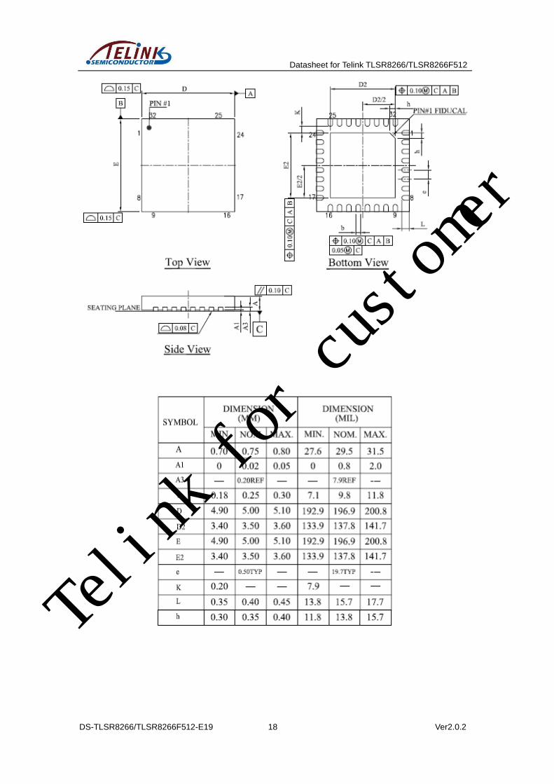
1.5 Package
For the TLSR8266, 56-pin QFN 7×7mm, 48-pin QFN 7×7mm and 32-pin QFN 5
×5mm package options are available. For the TLSR8266F512, 48-pin QFN 7×7mm
and 32-pin QFN 5×5mm package options are available. Package dimension for the
TLSR8266ET/AT56, the TLSR8266ET/AT48/TLSR8266F512ET/AT48 and the
TLSR8266ET/AT32/TLSR8266F512ET/AT32 are shown as Figure 1-2, Figure 1-3 and
Figure 1-4, respectively.
Telink for customer

Datasheet for Telink TLSR8266/TLSR8266F512
DS-TLSR8266/TLSR8266F512-E19 16 Ver2.0.2
Figure 1- 2 Package dimension for the TLSR8266ET/AT56 (Unit: mm)
Telink for customer

Datasheet for Telink TLSR8266/TLSR8266F512
DS-TLSR8266/TLSR8266F512-E19 17 Ver2.0.2
Figure 1- 3 Package dimension for the TLSR8266ET/AT48/
TLSR8266F512ET/AT48 (Unit: mm)
Telink for customer
Datasheet for Telink TLSR8266/TLSR8266F512
DS-TLSR8266/TLSR8266F512-E19 18 Ver2.0.2
Telink for customer

Datasheet for Telink TLSR8266/TLSR8266F512
DS-TLSR8266/TLSR8266F512-E19 19 Ver2.0.2
Figure 1- 4 Package dimension for the TLSR8266ET/AT32/
TLSR8266F512ET/AT32 (Unit: mm)
1.6 Pin layout
Pin assignment for the TLSR8266ET/AT56 is as shown in Figure 1-5:
1
2
3
4
5
6
7
8
9
11
12
13
14
56 55 54 53 52 51 50 49 48 47 46 45 44 43
40
39
38
37
36
35
34
33
32
31
30
29
42
41
15 16 17 18 19 20 21 22 23 24 25 26 27 28
10
SWS/ANA_A<0>
PWM3/ANA_A<1>
MSDI/ANA_A<2>
MCLK/ANA_A<3>
GP18/PWM3_N/ANA_A<4>
PWM4/ANA_A<5>
GP19/PWM4_N/ANA_A<6>
SWM/ANA_A<7>
PWM5/ANA_B<0>
GP20/PWM5_N/ANA_B<1>
MSDO/ANA_B<2>
MSCN/ANA_B<3>
DM/ANA_B<5>
DP/ANA_B<6>
VB
US
VD
DO
3
DV
DD
3
DV
SS
DV
SS
VD
DD
EC
GP
0/P
WM
0_N
/AN
A_B
<7
>
PW
M0/A
NA
_C
<0>
/Am
ic_B
ias
GP
1/P
WM
1_N
/AN
A_C
<1>
/Am
ic_In
PW
M1_N
/AN
A_C
<2>
GP
2/P
WM
1/A
NA
_C
<3>
PW
M2/A
NA
_C
<4>
GP
3/P
WM
2_N
/AN
A_C
<5>
GP
4/u
art_
tx/A
NA
_C
<6>
GP5/uart_rx/ANA_C<7>
GP6/uart_rts/ANA_D<0>
GP7/uart_cts/ANA_D<1>
GP8/PWM3/ANA_D<2>
GP9/PWM4/ANA_D<3>
GP10/ANA_D<4>
GP11/ANA_D<5>
GP12/ANA_D<6>/Rbias_EXT
XC2
AVDD3
XC1
AVDD3
NC
NC
AN
T
AV
DD
3
GP
13/A
NA
_D
<7>
GP
14/A
NA
_E
<0>
RE
SE
TB
DM
IC_C
K/A
NA
_E
<1>
DM
IC_D
I/A
NA
_E
<2>
GP
15/A
NA
_E
<3>
GP
16/S
DM
_P
/AN
A_E
<4>
GP
17/S
DM
_N
/AN
A_E
<5>
CN
/uar
t_rt
s/A
NA
_E
<6>
DI/
I2C
_S
DA
/AN
A_E
<7>
DO
/uar
t_ct
s/A
NA
_F
<0>
CK
/I2C
_S
CL
/AN
A_F
<1>
TLSR8266ET/AT56
Figure 1- 5 Pin assignment for the TLSR8266ET/AT56
Functions of 56pins for the TLSR8266ET/AT56 are described in Table 1-2:
Telink for customer

Datasheet for Telink TLSR8266/TLSR8266F512
DS-TLSR8266/TLSR8266F512-E19 20 Ver2.0.2
Table 1- 2 Pin functions for the TLSR8266ET/AT56
QFN56 7X7
No. Pin Name Type Description
1 SWS/ANA_A<0> Digital I/O Single wire slave/GPIO/ANA_A<0>
2 PWM3/ANA_A<1> Digital I/O PWM3 output/GPIO/ ANA_A<1>
3 MSDI/ANA_A<2> Digital I/O Memory SPI data input/GPIO/ANA_A<2>
4 MCLK/ANA_A<3> Digital I/O Memory SPI clock/GPIO/ANA_A<3>
5 GP18/PWM3_N/ANA_A<4> Digital I/O GPIO18/PWM3 inverting output/ANA_A<4>
6 PWM4/ANA_A<5> Digital I/O PWM4 output/GPIO/ANA_A<5>
7 GP19/PWM4_N/ANA_A<6> Digital I/O GPIO19/PWM4 inverting output/ANA_A<6>
8 SWM/ANA_A<7> Digital I/O Single Wire Master/GPIO/ANA_A<7>
9 PWM5/ANA_B<0> Digital I/O PWM5 output/GPIO/ANA_B<0>
10 GP20/PWM5_N/ANA_B<1> Digital I/O GPIO20/PWM5 inverting output/ ANA_B<1>
11 MSDO/ANA_B<2> Digital I/O Memory SPI data output/GPIO/ANA_B<2>
12 MSCN/ANA_B<3> Digital I/O Memory SPI chip-select(Active low)/GPIO/
ANA_B<3>
13 DM/ANA_B<5> Digital I/O USB data Minus/GPIO/ANA_B<5>
14 DP/ANA_B<6> Digital I/O USB data Positive/GPIO/ANA_B<6>
15 VBUS PWR USB 5V supply
16 VDDO3 PWR 5V-to-3V LDO output
17 DVDD3 PWR 3.3V IO supply
18 DVSS GND Digital LDO ground
19 VDDDEC PWR Digital LDO 1.8V output
20 DVSS GND Digital LDO ground
21 GP0/PWM0_N/ANA_B<7> Digital I/O GPIO0/ PWM0 inverting output /ANA_B<7>
22 PWM0/ANA_C<0>/Amic_Bias Digital I/O PWM0 output/GPIO/ANA_C<0>/Analog
microphone Bias
23 GP1/PWM1_N/ANA_C<1>/
Amic_In Digital I/O
GPIO1/PWM1 inverting output/ANA_C<1>/Analog microphone input
24 PWM1_N/ANA_C<2> Digital I/O PWM1 inverting output/GPIO/ANA_C<2>
25 GP2/PWM1/ANA_C<3> Digital I/O GPIO2/PWM1 output/ANA_C<3>
26 PWM2/ANA_C<4> Digital I/O PWM2 output/GPIO/ ANA_C<4>
27 GP3/PWM2_N/ANA_C<5> Digital I/O GPIO3/PWM2 inverting output/ ANA_C<5>
28 GP4/uart_tx/ANA_C<6> Digital I/O GPIO4/UART_TX/ ANA_C<6>
29 GP5/uart_rx/ANA_C<7> Digital I/O GPIO5/UART_RX/ ANA_C<7>
30 GP6/uart_rts/ANA_D<0> Digital I/O GPIO6/UART_RTS / ANA_D<0>
31 GP7/uart_cts/ANA_D<1> Digital I/O GPIO7/UART_CTS / ANA_D<1>
32 GP8/PWM3/ANA_D<2> Digital I/O GPIO8/ PWM3 output/ ANA_D<2>
33 GP9/PWM4/ANA_D<3> Digital I/O GPIO9/ PWM4 output/ ANA_D<3>
34 GP10/ANA_D<4> Digital I/O GPIO10/ ANA_D<4>
35 GP11/ANA_D<5> Digital I/O GPIO11/ ANA_D<5>
Telink for customer

Datasheet for Telink TLSR8266/TLSR8266F512
DS-TLSR8266/TLSR8266F512-E19 21 Ver2.0.2
QFN56 7X7
No. Pin Name Type Description
36 GP12/ANA_D<6>/Rbias_EXT Digital I/O GPIO12/ ANA_D<6>/off-chip bias resistor
37 AVDD3 PWR Analog 3.3V supply
38 XC2 Analog O 12MHz/16MHz crystal output
39 XC1 Analog I 12MHz/16MHz crystal input
40 AVDD3 PWR Analog 3.3V supply
41 NC Not connected
42 NC Not connected
43 ANT Analog I/O RF antenna
44 AVDD3 PWR Analog 3.3V supply
45 GP13/ANA_D<7> Digital I/O GPIO13/ ANA_D<7>
46 GP14/ANA_E<0> Digital I/O GPIO14/ ANA_E<0>
47 RESETB RESET Power on reset, active low
48 DMIC_CK/ANA_E<1> Digital I/O DMIC clock/GPIO/ANA_E<1>
49 DMIC_DI/ANA_E<2> Digital I/O DMIC data input/ GPIO/ANA_E<2>
50 GP15/ANA_E<3> Digital I/O GPIO15/ ANA_E<3>
51 GP16/SDM_P/ANA_E<4> Digital I/O GPIO16/ ANA_E<4>
52 GP17/SDM_N/ANA_E<5> Digital I/O GPIO17/ ANA_E<5>
53 CN/uart_rts/ANA_E<6> Digital I/O SPI chip select. Active low/ UART_RTS /GPIO/
ANA_E<6>
54 DI/I2C_SDA/ANA_E<7> Digital I/O SPI data input/I2C_SDA/GPIO/ ANA_E<7>
55 DO/uart_cts/ANA_F<0> Digital I/O SPI data output/ UART_CTS /GPIO/
ANA_F<0>
56 CK/I2C_SCL/ANA_F<1> Digital I/O SPI clock/I2C_SCK/GPIO/ ANA_F<1>
*Note:
1) Pins with bold typeface can be used as GPIOS. All GPIOs have configurable
pull-up/pull-down resistor.
2) Pin drive strength: All pins support drive strength up to 4mA (4mA when “DS”=1,
0.7mA when “DS”=0) with the following exceptions: ANA_B<6> and ANA_B<5>
support high drive strength up to 8mA (8mA when “DS”=1, 4mA when “DS”=0);
ANA_E<5> and ANA_E<4> support high drive strength up to 16mA (16mA when
“DS”=1, 12mA when “DS”=0). “DS” configuration will take effect when the pin is used
as output. Please refer to section 7.1 for corresponding “DS” register address and the
default setting.
Telink for customer

Datasheet for Telink TLSR8266/TLSR8266F512
DS-TLSR8266/TLSR8266F512-E19 22 Ver2.0.2
Pin assignment for the TLSR8266ET/AT48 is as shown in Figure 1-6:
1
2
3
4
5
6
7
8
9
10
11
12
36
35
34
33
32
31
30
29
28
27
26
25
48 47 46 45 44 43 42 41 40 39 38 37
13 14 15 16 17 18 19 20 21 22 23 24
SWS/ANA_A<0>
PWM3/ANA_A<1>
MSDI/ANA_A<2>
MCLK/ANA_A<3>
PWM4/ANA_A<5>
GP19/PWM4_N/ANA_A<6>
SWM/ANA_A<7>
PWM5/ANA_B<0>
MSDO/ANA_B<2>
DM/ANA_B<5>
DP/ANA_B<6>
DV
DD
3
DV
SS
VD
DD
EC
DV
SS
GP
0/P
WM
0_
N/A
NA
_B
<7
>
PW
M0
/AN
A_
C<
0>
/Am
ic_
Bia
s
GP
1/P
WM
1_
N/A
NA
_C
<1
>/A
mic
_In
PW
M1
_N
/AN
A_
C<
2>
GP
2/P
WM
1/A
NA
_C
<3
>
PW
M2
/AN
A_
C<
4>
GP
3/P
WM
2_
N/A
NA
_C
<5
>
GP
4/u
art_
tx/A
NA
_C
<6
>GP5/uart_rx/ANA_C<7>
XC1
GP7/uart_cts/ANA_D<1>
GP8/PWM3/ANA_D<2>
GP9/PWM4/ANA_D<3>
GP12/ANA_D<6>/Rbias_EXT
AVDD3
XC2
AVDD3
GP6/uart_rts/ANA_D<0>
AN
T
AV
DD
3
GP
13
/AN
A_
D<
7>
RE
SE
TB
DM
IC_
CK
/AN
A_
E<
1>
DM
IC_
DI/
AN
A_
E<
2>
GP
16
/SD
M_
P/A
NA
_E
<4>
GP
17
/SD
M_
N/A
NA
_E
<5
>
CN
/uar
t_rt
s/A
NA
_E
<6
>
DI/
I2C
_S
DA
/AN
A_
E<
7>
DO
/uar
t_ct
s/A
NA
_F
<0
>
CK
/I2
C_
SC
L/A
NA
_F
<1
>
TLSR8266ET/AT48
MSCN/ANA_B<3>
GP10/ANA_D<4>
GP11/ANA_D<5>
Figure 1- 6 Pin assignment for the TLSR8266ET/AT48
Functions of 48 pins for the TLSR8266ET/AT48 are described in Table 1-3:
Table 1- 3 Pin functions for the TLSR8266ET/AT48
QFN48 7X7
No. Pin Name Type Description
1 SWS/ANA_A<0> Digital
I/O Single wire slave/GPIO/ANA_A<0>
2 PWM3/ANA_A<1> Digital
I/O PWM3 output/GPIO/ ANA_A<1>
3 MSDI/ANA_A<2> Digital
I/O Memory SPI data input/GPIO/ANA_A<2>
4 MCLK/ANA_A<3> Digital
I/O Memory SPI clock/GPIO/ANA_A<3>
5 PWM4/ANA_A<5> Digital
I/O PWM4 output/GPIO/ANA_A<5>
Telink for customer

Datasheet for Telink TLSR8266/TLSR8266F512
DS-TLSR8266/TLSR8266F512-E19 23 Ver2.0.2
QFN48 7X7
No. Pin Name Type Description
6 GP19/PWM4_N/ANA_A<6> Digital
I/O GPIO19/PWM4 inverting output/ANA_A<6>
7 SWM/ANA_A<7> Digital
I/O Single Wire Master/GPIO/ANA_A<7>
8 PWM5/ANA_B<0> Digital
I/O PWM5 output/GPIO/ANA_B<0>
9 MSDO/ANA_B<2> Digital
I/O Memory SPI data output/GPIO/ANA_B<2>
10 MSCN/ANA_B<3> Digital
I/O Memory SPI chip-select(Active low)/GPIO/
ANA_B<3>
11 DM/ANA_B<5> Digital
I/O USB data Minus/GPIO/ANA_B<5>
12 DP/ANA_B<6> Digital
I/O USB data Positive/GPIO/ANA_B<6>
13 DVDD3 PWR 3.3V IO supply
14 DVSS GND Digital LDO ground
15 VDDDEC PWR Digital LDO 1.8V output
16 DVSS GND Digital LDO ground
17 GP0/PWM0_N/ANA_B<7> Digital
I/O GPIO0/PWM0 inverting output/ANA_B<7>
18 PWM0/ANA_C<0>/Amic_Bias Digital
I/O PWM0 output/GPIO/ANA_C<0>/ Analog
microphone Bias
19 GP1/PWM1_N/ANA_C<1>/
Amic_In
Digital I/O
GPIO1/PWM1 inverting output/ANA_C<1>/Analog microphone input
20 PWM1_N/ANA_C<2> Digital
I/O PWM1 inverting output/GPIO/ANA_C<2>
21 GP2/PWM1/ANA_C<3> Digital
I/O GPIO2/PWM1 output/ANA_C<3>
22 PWM2/ANA_C<4> Digital
I/O PWM2 output/GPIO/ ANA_C<4>
23 GP3/PWM2_N/ANA_C<5> Digital
I/O GPIO3/PWM2 inverting output/ ANA_C<5>
24 GP4/uart_tx/ANA_C<6> Digital
I/O GPIO4/UART_TX/ ANA_C<6>
25 GP5/uart_rx/ANA_C<7> Digital
I/O GPIO5/UART_RX/ ANA_C<7>
26 GP6/uart_rts/ANA_D<0> Digital
I/O GPIO6/UART_RTS / ANA_D<0>
27 GP7/uart_cts/ANA_D<1> Digital
I/O GPIO7/UART_CTS / ANA_D<1>
28 GP8/PWM3/ANA_D<2> Digital
I/O GPIO8/ PWM3 output/ANA_D<2>
29 GP9/PWM4/ANA_D<3> Digital
I/O GPIO9/ PWM4 output/ANA_D<3>
30 GP10/ANA_D<4> GPIO10/ ANA_D<4>
31 GP11/ANA_D<5> GPIO11/ ANA_D<5>
Telink for customer

Datasheet for Telink TLSR8266/TLSR8266F512
DS-TLSR8266/TLSR8266F512-E19 24 Ver2.0.2
QFN48 7X7
No. Pin Name Type Description
32 GP12/ANA_D<6>/Rbias_EXT Digital
I/O GPIO12/ ANA_D<6>/off-chip bias resistor
33 AVDD3 PWR Analog 3.3V supply
34 XC2 Analog
O 12MHz/16MHz crystal output
35 XC1 Analog
I 12MHz/16MHz crystal input
36 AVDD3 PWR Analog 3.3V supply
37 ANT Analog
O RF antenna
38 AVDD3 PWR Analog 3.3V supply
39 GP13/ANA_D<7> Digital
I/O GPIO13/ ANA_D<7>
40 RESETB RESET Power on reset, active low
41 DMIC_CK/ANA_E<1> Digital
I/O DMIC clock/GPIO/ANA_E<1>
42 DMIC_DI/ANA_E<2> Digital
I/O DMIC data input/GPIO/ ANA_E<2>
43 GP16/SDM_P/ANA_E<4> Digital
I/O GPIO16/ ANA_E<4>
44 GP17/SDM_N/ANA_E<5> Digital
I/O GPIO17/ ANA_E<5>
45 CN/uart_rts/ANA_E<6> Digital
I/O SPI chip select. Active low/ UART_RTS /GPIO/
ANA_E<6>
46 DI/I2C_SDA/ANA_E<7> Digital
I/O SPI data input/I2C_SDA/GPIO/ ANA_E<7>
47 DO/uart_cts/ANA_F<0> Digital
I/O SPI data output/ UART_CTS /GPIO/ ANA_F<0>
48 CK/I2C_SCL/ANA_F<1> Digital
I/O SPI clock/I2C_SCK/GPIO/ ANA_F<1>
*Note:
1) Pins with bold typeface can be used as GPIOS. All GPIOs have configurable
pull-up/pull-down resistor.
2) Pin drive strength: All pins support drive strength up to 4mA (4mA when “DS”=1,
0.7mA when “DS”=0) with the following exceptions: ANA_B<6> and ANA_B<5>
support high drive strength up to 8mA (8mA when “DS”=1, 4mA when “DS”=0);
ANA_E<5> and ANA_E<4> support high drive strength up to 16mA (16mA when
“DS”=1, 12mA when “DS”=0). “DS” configuration will take effect when the pin is used
as output. Please refer to section 7.1 for corresponding “DS” register address and the
default setting.
Telink for customer

Datasheet for Telink TLSR8266/TLSR8266F512
DS-TLSR8266/TLSR8266F512-E19 25 Ver2.0.2
Pin assignment for the TLSR8266ET/AT32 is as shown in Figure 1-7:
1
2
3
4
5
6
7
8
24
23
22
21
20
19
18
17
9 1110 12 13 14 1615
32 3031 29 28 27 2526
SWS/ANA_A<0>
DV
DD
3
DV
SS
VD
DD
EC
GP5/uart_rx/ANA_C<7>
XC1
XC2
AVDD3
AV
DD
3
RE
SE
TB
TLSR8266ET/AT32
PWM3/ANA_A<1>
MSDI/ANA_A<2>
MCLK/ANA_A<3>
MSDO/ANA_B<2>
MSCN/ANA_B<3>
DM/ANA_B<5>
DP/ANA_B<6>
PW
M0
/AN
A_
C<
0>
/Am
ic_
Bia
s
GP
1/P
WM
1_
N/A
NA
_C
<1>
/Am
ic_
In
PW
M1
_N
/AN
A_
C<
2>
PW
M2
/AN
A_
C<
4>
AVDD3
CN
/uar
t_rt
s/A
NA
_E
<6
>
DI/
I2C
_S
DA
/AN
A_
E<
7>
DO
/uar
t_ct
s/A
NA
_F
<0
>
CK
/I2
C_
SC
L/A
NA
_F
<1
>
GP10/ANA_D<4>
GP11/ANA_D<5>
GP
4/u
art_
tx/A
NA
_C
<6
>
ANT
DM
IC_
CK
/AN
A_
E<
1>
DM
IC_
DI/
AN
A_
E<
2>
Figure 1- 7 Pin assignment for the TLSR8266ET/AT32
Functions of 32 pins for the TLSR8266ET/AT32 are described in Table 1-4:
Table 1- 4 Pin functions for the TLSR8266ET/AT32
QFN32 5X5
No. Pin Name Pin Type Description
1 SWS/ANA_A<0> Digital I/O Single wire slave/GPIO/ANA_A<0>
2 PWM3/ANA_A<1> Digital I/O PWM3 output/GPIO/ ANA_A<1>
3 MSDI/ANA_A<2> Digital I/O Memory SPI data input/GPIO/ANA_A<2>
4 MCLK/ANA_A<3> Digital I/O Memory SPI clock/GPIO/ANA_A<3>
5 MSDO/ANA_B<2> Digital I/O Memory SPI data output/GPIO/ANA_B<2>
Telink for customer

Datasheet for Telink TLSR8266/TLSR8266F512
DS-TLSR8266/TLSR8266F512-E19 26 Ver2.0.2
QFN32 5X5
No. Pin Name Pin Type Description
6 MSCN/ANA_B<3> Digital I/O Memory SPI chip-select(Active low)/GPIO/
ANA_B<3>
7 DM/ANA_B<5> Digital I/O USB data Minus/GPIO/ANA_B<5>
8 DP/ANA_B<6> Digital I/O USB data Positive/GPIO/ANA_B<6>
9 DVDD3 PWR 3.3V IO supply
10 DVSS GND Digital LDO ground
11 VDDDEC PWR Digital LDO 1.8V output
12 PWM0/ANA_C<0>/
Amic_Bias Digital I/O
PWM0 output/GPIO/ANA_C<0>/ Analog microphone Bias
13 GP1/PWM1_N/
ANA_C<1>/Amic_In Digital I/O
GPIO1/PWM1 inverting output/ANA_C<1>/Analog microphone input
14 PWM1_N/ANA_C<2> Digital I/O PWM1 inverting output/GPIO/ANA_C<2>
15 PWM2/ANA_C<4> Digital I/O PWM2 output/GPIO/ ANA_C<4>
16 GP4/uart_tx/ANA_C<6> Digital I/O GPIO4/UART_TX/ ANA_C<6>
17 GP5/uart_rx/ANA_C<7> Digital I/O GPIO5/UART_RX/ ANA_C<7>
18 GP10/ANA_D<4> Digital I/O GPIO10/ ANA_D<4>
19 GP11/ANA_D<5> Digital I/O GPIO11/ ANA_D<5>
20 AVDD3 PWR Analog 3.3V supply
21 XC2 Analog O 12MHz/16MHz crystal output
22 XC1 Analog I 12MHz/16MHz crystal input
23 AVDD3 PWR Analog 3.3V supply
24 ANT Analog
I/O RF antenna
25 AVDD3 PWR Analog 3.3V supply
26 RESETB RESET Power on reset, active low
27 DMIC_CK/ANA_E<1> Digital I/O DMIC clock/GPIO/ANA_E<1>
28 DMIC_DI/ANA_E<2> Digital I/O DMIC data input/GPIO/ ANA_E<2>
29 CN/uart_rts/ANA_E<6> Digital I/O SPI chip select. Active low/ UART_RTS /GPIO/
ANA_E<6>
30 DI/I2C_SDA/ANA_E<7> Digital I/O SPI data input/I2C_SDA/GPIO/ ANA_E<7>
31 DO/uart_cts/ANA_F<0> Digital I/O SPI data output/ UART_CTS /GPIO/ ANA_F<0>
32 CK/I2C_SCL/ANA_F<1> Digital I/O SPI clock/I2C_SCK/GPIO/ ANA_F<1>
*Note:
1) Pins with bold typeface can be used as GPIOS. All GPIOs have configurable
pull-up/pull-down resistor.
2) Pin drive strength: All pins support drive strength up to 4mA (4mA when “DS”=1,
0.7mA when “DS”=0) with the following exceptions: ANA_B<6> and ANA_B<5>
support high drive strength up to 8mA (8mA when “DS”=1, 4mA when “DS”=0). “DS”
configuration will take effect when the pin is used as output. Please refer to section
7.1 for corresponding “DS” register address and the default setting.
Telink for customer

Datasheet for Telink TLSR8266/TLSR8266F512
DS-TLSR8266/TLSR8266F512-E19 27 Ver2.0.2
Pin assignment for the TLSR8266F512ET/AT48 is as shown in Figure 1-8:
1
2
3
4
5
6
7
8
9
10
11
12
36
35
34
33
32
31
30
29
28
27
26
25
48 47 46 45 44 43 42 41 40 39 38 37
13 14 15 16 17 18 19 20 21 22 23 24
SWS/ANA_A<0>
PWM3/ANA_A<1>
3-12
GP18/PWM3_N/ANA_A<4>
PWM4/ANA_A<5>
GP19/PWM4_N/ANA_A<6>
SWM/ANA_A<7>
PWM5/ANA_B<0>
GP20/PWM5_N/ANA_B<1>
DM/ANA_B<5>
DP/ANA_B<6>
12-3
DV
DD
3
DV
SS
VD
DD
EC
DV
SS
GP
0/P
WM
0_
N/A
NA
_B
<7
>
PW
M0
/AN
A_
C<
0>
/Am
ic_B
ias
GP
1/P
WM
1_
N/A
NA
_C
<1
>/A
mic
_In
PW
M1
_N
/AN
A_
C<
2>
GP
2/P
WM
1/A
NA
_C
<3
>
PW
M2
/AN
A_
C<
4>
GP
3/P
WM
2_
N/A
NA
_C
<5
>
GP
4/u
art_
tx/A
NA
_C
<6
>
GP5/uart_rx/ANA_C<7>
XC1
GP7/uart_cts/ANA_D<1>
GP8/PWM3/ANA_D<2>
GP9/PWM4/ANA_D<3>
GP12/ANA_D<6>/Rbias_EXT
AVDD3
XC2
AVDD3
GP6/uart_rts/ANA_D<0>A
NT
AV
DD
3
GP
13
/AN
A_
D<
7>
RE
SE
TB
DM
IC_
CK
/AN
A_
E<
1>
DM
IC_
DI/
AN
A_
E<
2>
GP
16
/SD
M_
P/A
NA
_E
<4
>
GP
17
/SD
M_
N/A
NA
_E
<5
>
CN
/uar
t_rt
s/A
NA
_E
<6
>
DI/
I2C
_S
DA
/AN
A_
E<
7>
DO
/uar
t_ct
s/A
NA
_F
<0
>
CK
/I2
C_
SC
L/A
NA
_F
<1
>
TLSR8266F512ET/AT48GP10/ANA_D<4>
GP11/ANA_D<5>
Figure 1- 8 Pin assignment for the TLSR8266F512ET/AT48
Functions of 48 pins for the TLSR8266F512ET/AT48 are described in Table 1-5:
Table 1- 5 Pin functions for the TLSR8266F512ET/AT48
QFN48 7X7
No. Pin Name Type Description
1 SWS/ANA_A<0> Digital
I/O Single wire slave/GPIO/ANA_A<0>
2 PWM3/ANA_A<1> Digital
I/O PWM3 output/GPIO/ ANA_A<1>
3 3-12 - This pin should be connected to Pin #12
4 GP18/PWM3_N/ANA_A<4> Digital
I/O GPIO18/PWM3 inverting output/ANA_A<4>
Telink for customer
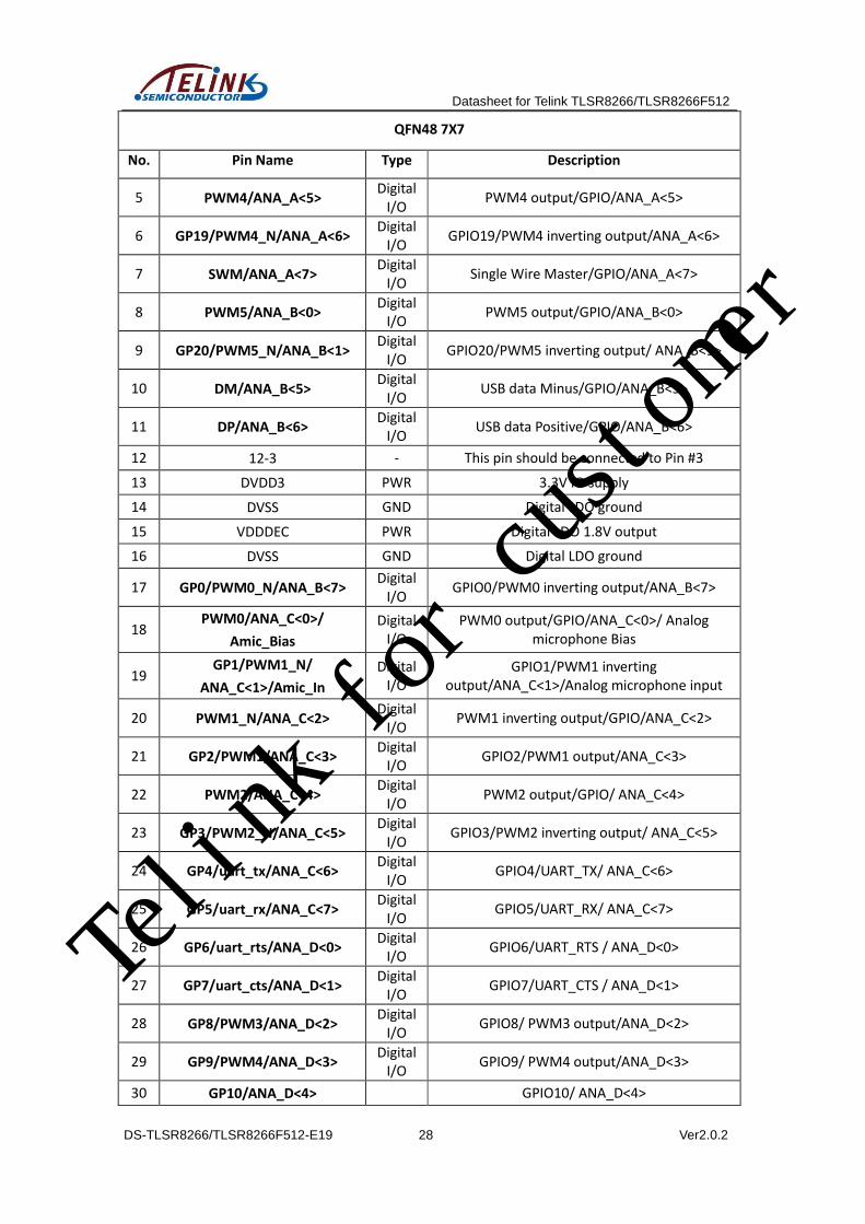
Datasheet for Telink TLSR8266/TLSR8266F512
DS-TLSR8266/TLSR8266F512-E19 28 Ver2.0.2
QFN48 7X7
No. Pin Name Type Description
5 PWM4/ANA_A<5> Digital
I/O PWM4 output/GPIO/ANA_A<5>
6 GP19/PWM4_N/ANA_A<6> Digital
I/O GPIO19/PWM4 inverting output/ANA_A<6>
7 SWM/ANA_A<7> Digital
I/O Single Wire Master/GPIO/ANA_A<7>
8 PWM5/ANA_B<0> Digital
I/O PWM5 output/GPIO/ANA_B<0>
9 GP20/PWM5_N/ANA_B<1> Digital
I/O GPIO20/PWM5 inverting output/ ANA_B<1>
10 DM/ANA_B<5> Digital
I/O USB data Minus/GPIO/ANA_B<5>
11 DP/ANA_B<6> Digital
I/O USB data Positive/GPIO/ANA_B<6>
12 12-3 - This pin should be connected to Pin #3
13 DVDD3 PWR 3.3V IO supply
14 DVSS GND Digital LDO ground
15 VDDDEC PWR Digital LDO 1.8V output
16 DVSS GND Digital LDO ground
17 GP0/PWM0_N/ANA_B<7> Digital
I/O GPIO0/PWM0 inverting output/ANA_B<7>
18 PWM0/ANA_C<0>/
Amic_Bias
Digital I/O
PWM0 output/GPIO/ANA_C<0>/ Analog microphone Bias
19 GP1/PWM1_N/
ANA_C<1>/Amic_In
Digital I/O
GPIO1/PWM1 inverting output/ANA_C<1>/Analog microphone input
20 PWM1_N/ANA_C<2> Digital
I/O PWM1 inverting output/GPIO/ANA_C<2>
21 GP2/PWM1/ANA_C<3> Digital
I/O GPIO2/PWM1 output/ANA_C<3>
22 PWM2/ANA_C<4> Digital
I/O PWM2 output/GPIO/ ANA_C<4>
23 GP3/PWM2_N/ANA_C<5> Digital
I/O GPIO3/PWM2 inverting output/ ANA_C<5>
24 GP4/uart_tx/ANA_C<6> Digital
I/O GPIO4/UART_TX/ ANA_C<6>
25 GP5/uart_rx/ANA_C<7> Digital
I/O GPIO5/UART_RX/ ANA_C<7>
26 GP6/uart_rts/ANA_D<0> Digital
I/O GPIO6/UART_RTS / ANA_D<0>
27 GP7/uart_cts/ANA_D<1> Digital
I/O GPIO7/UART_CTS / ANA_D<1>
28 GP8/PWM3/ANA_D<2> Digital
I/O GPIO8/ PWM3 output/ANA_D<2>
29 GP9/PWM4/ANA_D<3> Digital
I/O GPIO9/ PWM4 output/ANA_D<3>
30 GP10/ANA_D<4> GPIO10/ ANA_D<4>
Telink for customer

Datasheet for Telink TLSR8266/TLSR8266F512
DS-TLSR8266/TLSR8266F512-E19 29 Ver2.0.2
QFN48 7X7
No. Pin Name Type Description
31 GP11/ANA_D<5> GPIO11/ ANA_D<5>
32 GP12/ANA_D<6>/Rbias_EXT Digital
I/O GPIO12/ ANA_D<6>/off-chip bias resistor
33 AVDD3 PWR Analog 3.3V supply
34 XC2 Analog
O 12MHz/16MHz crystal output
35 XC1 Analog
I 12MHz/16MHz crystal input
36 AVDD3 PWR Analog 3.3V supply
37 ANT Analog
O RF antenna
38 AVDD3 PWR Analog 3.3V supply
39 GP13/ANA_D<7> Digital
I/O GPIO13/ ANA_D<7>
40 RESETB RESET Power on reset, active low
41 DMIC_CK/ANA_E<1> Digital
I/O DMIC clock/GPIO/ANA_E<1>
42 DMIC_DI/ANA_E<2> Digital
I/O DMIC data input/GPIO/ ANA_E<2>
43 GP16/SDM_P/ANA_E<4> Digital
I/O GPIO16/ ANA_E<4>
44 GP17/SDM_N/ANA_E<5> Digital
I/O GPIO17/ ANA_E<5>
45 CN/uart_rts/ANA_E<6> Digital
I/O SPI chip select. Active low/ UART_RTS /GPIO/
ANA_E<6>
46 DI/I2C_SDA/ANA_E<7> Digital
I/O SPI data input/I2C_SDA/GPIO/ ANA_E<7>
47 DO/uart_cts/ANA_F<0> Digital
I/O SPI data output/ UART_CTS /GPIO/ ANA_F<0>
48 CK/I2C_SCL/ANA_F<1> Digital
I/O SPI clock/I2C_SCK/GPIO/ ANA_F<1>
*Note:
1) Pins with bold typeface can be used as GPIOS. All GPIOs have configurable
pull-up/pull-down resistor.
2) Pin drive strength: All pins support drive strength up to 4mA (4mA when “DS”=1,
0.7mA when “DS”=0) with the following exceptions: ANA_B<6> and ANA_B<5>
support high drive strength up to 8mA (8mA when “DS”=1, 4mA when “DS”=0);
ANA_E<5> and ANA_E<4> support high drive strength up to 16mA (16mA when
“DS”=1, 12mA when “DS”=0). “DS” configuration will take effect when the pin is used
as output. Please refer to section 7.1 for corresponding “DS” register address and the
default setting.
Telink for customer

Datasheet for Telink TLSR8266/TLSR8266F512
DS-TLSR8266/TLSR8266F512-E19 30 Ver2.0.2
Pin assignment for the TLSR8266F512ET/AT32 is as shown in Figure 1-9:
1
2
3
4
5
6
7
8
24
23
22
21
20
19
18
17
9 1110 12 13 14 1615
32 3031 29 28 27 2526
SWS/ANA_A<0>D
VD
D3
DV
SS
VD
DD
EC
GP5/uart_rx/ANA_C<7>
XC1
XC2
AVDD3
AV
DD
3
RE
SE
TB
TLSR8266F512ET/AT32
PWM3/ANA_A<1>
3-8
PWM4/ANA_A<5>
PWM5/ANA_B<0>
DM/ANA_B<5>
DP/ANA_B<6>
PW
M0
/AN
A_
C<
0>
/Am
ic_
Bia
s
GP
1/P
WM
1_
N/A
NA
_C
<1>
/Am
ic_
In
PW
M1
_N
/AN
A_
C<
2>
PW
M2
/AN
A_
C<
4>
AVDD3
CN
/uar
t_rt
s/A
NA
_E
<6
>
DI/
I2C
_S
DA
/AN
A_
E<
7>
DO
/uar
t_ct
s/A
NA
_F
<0
>
CK
/I2
C_
SC
L/A
NA
_F
<1
>
GP10/ANA_D<4>
GP11/ANA_D<5>
GP
4/u
art_
tx/A
NA
_C
<6
>
ANT
GP
16
/SD
M_
P/A
NA
_E
<4>
GP
17
/SD
M_
N/A
NA
_E
<5
>
8-3
Figure 1- 9 Pin assignment for the TLSR8266F512ET/AT32
Functions of 32 pins for the TLSR8266F512ET/AT32 are described in Table 1-6:
Table 1- 6 Pin functions for the TLSR8266F512ET/AT32
QFN32 5X5
No. Pin Name Type Description
1 SWS/ANA_A<0> Digital I/O Single wire slave/GPIO/ANA_A<0>
2 PWM3/ANA_A<1> Digital I/O PWM3 output/GPIO/ ANA_A<1>
3 3-8 - This pin should be connected to Pin #8
4 PWM4/ANA_A<5> Digital I/O PWM4 output/GPIO/ANA_A<5>
5 PWM5/ANA_B<0> Digital I/O PWM5 output/GPIO/ANA_B<0>
6 DM/ANA_B<5> Digital I/O USB data Minus/GPIO/ANA_B<5>
Telink for customer

Datasheet for Telink TLSR8266/TLSR8266F512
DS-TLSR8266/TLSR8266F512-E19 31 Ver2.0.2
QFN32 5X5
No. Pin Name Type Description
7 DP/ANA_B<6> Digital I/O USB data Positive/GPIO/ANA_B<6>
8 8-3 - This pin should be connected to Pin #3
9 DVDD3 PWR 3.3V IO supply
10 DVSS GND Digital LDO ground
11 VDDDEC PWR Digital LDO 1.8V output
12 PWM0/ANA_C<0>/Amic_Bias Digital I/O PWM0 output/GPIO/ANA_C<0>/Analog
microphone Bias
13 GP1/PWM1_N/ANA_C<1>/
Amic_In Digital I/O
GPIO1/PWM1 inverting output/ANA_C<1>/Analog microphone input
14 PWM1_N/ANA_C<2> Digital I/O PWM1 inverting output/GPIO/ANA_C<2>
15 PWM2/ANA_C<4> Digital I/O PWM2 output/GPIO/ ANA_C<4>
16 GP4/uart_tx/ANA_C<6> Digital I/O GPIO4/UART_TX/ ANA_C<6>
17 GP5/uart_rx/ANA_C<7> Digital I/O GPIO5/UART_RX/ ANA_C<7>
18 GP10/ANA_D<4> Digital I/O GPIO10/ ANA_D<4>
19 GP11/ANA_D<5> Digital I/O GPIO11/ ANA_D<5>
20 AVDD3 PWR Analog 3.3V supply
21 XC2 Analog O 12MHz/16MHz crystal output
22 XC1 Analog I 12MHz/16MHz crystal input
23 AVDD3 PWR Analog 3.3V supply
24 ANT Analog I/O RF antenna
25 AVDD3 PWR Analog 3.3V supply
26 RESETB RESET Power on reset, active low
27 GP16/SDM_P/ANA_E<4> Digital I/O GPIO16/ ANA_E<4>
28 GP17/SDM_N/ANA_E<5> Digital I/O GPIO17/ ANA_E<5>
29 CN/uart_rts/ANA_E<6> Digital I/O SPI chip select. Active low/ UART_RTS /GPIO/
ANA_E<6>
30 DI/I2C_SDA/ANA_E<7> Digital I/O SPI data input/I2C_SDA/GPIO/ ANA_E<7>
31 DO/uart_cts/ANA_F<0> Digital I/O SPI data output/ UART_CTS /GPIO/
ANA_F<0>
32 CK/I2C_SCL/ANA_F<1> Digital I/O SPI clock/I2C_SCK/GPIO/ ANA_F<1>
*Note:
1) Pins with bold typeface can be used as GPIOS. All GPIOs have configurable
pull-up/pull-down resistor.
2) Pin drive strength: All pins support drive strength up to 4mA (4mA when “DS”=1,
0.7mA when “DS”=0) with the following exceptions: ANA_B<6> and ANA_B<5>
support high drive strength up to 8mA (8mA when “DS”=1, 4mA when “DS”=0);
ANA_E<5> and ANA_E<4> support high drive strength up to 16mA (16mA when
“DS”=1, 12mA when “DS”=0). “DS” configuration will take effect when the pin is used
as output. Please refer to section 7.1 for corresponding “DS” register address and the
default setting.
Telink for customer

Datasheet for Telink TLSR8266/TLSR8266F512
DS-TLSR8266/TLSR8266F512-E19 32 Ver2.0.2
1.7 Telink SDK
A full featured SDK is provided with the chip for Bluetooth Low Energy
applications. The customers can easily develop rich BLE applications by employing the
firmware, along with the system configuration data composed according to the
specific hardware design.
Telink for customer

Datasheet for Telink TLSR8266/TLSR8266F512
DS-TLSR8266/TLSR8266F512-E19 33 Ver2.0.2
2 Memory and MCU
2.1 Memory
The TLSR8266/TLSR8266F512 embeds 16KB data memory (SRAM), and
128/256/512KB selectable FLASH.
SRAM/Register memory map is shown as follows:
0x808000
0x80BFFF
0x80C000
16KB SRAM
0x807FFF
0x800000
Register
Figure 2- 1 Physical memory map
Register address: from 0x800000 to 0x807FFF;
16KB SRAM address: from 0x808000 to 0x80C000.
Both register and 16KB SRAM address can be accessed via SPI/I2C, SWS/SWM
interface.
FLASH address mapping is configurable. FLASH address can be accessed via MSPI
interface.
SPI FLASH
SRAM
0x0000
0x800000
0x7FFFFF
IO
Configurable
0xFFFFFF
Figure 2- 2 MCU memory map
Telink for customer
Datasheet for Telink TLSR8266/TLSR8266F512
DS-TLSR8266/TLSR8266F512-E19 34 Ver2.0.2
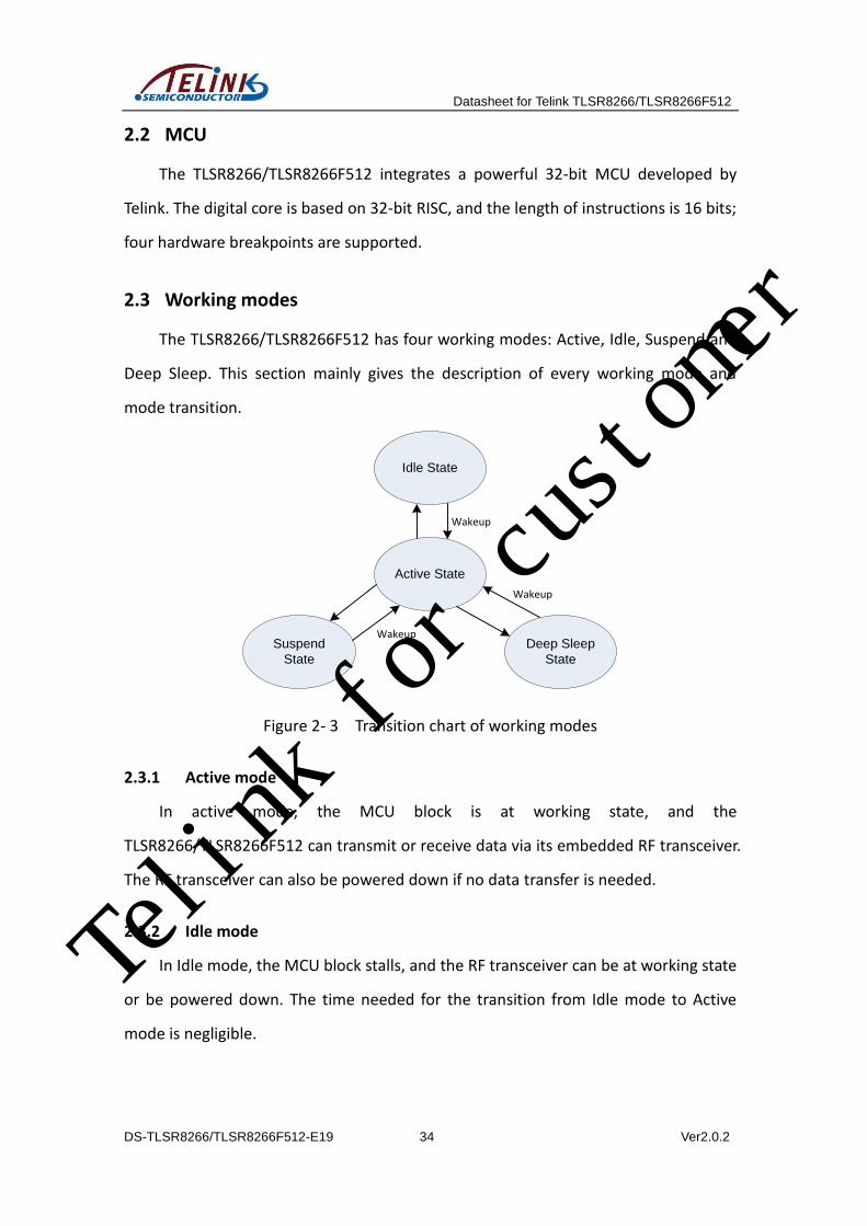
2.2 MCU
The TLSR8266/TLSR8266F512 integrates a powerful 32-bit MCU developed by
Telink. The digital core is based on 32-bit RISC, and the length of instructions is 16 bits;
four hardware breakpoints are supported.
2.3 Working modes
The TLSR8266/TLSR8266F512 has four working modes: Active, Idle, Suspend and
Deep Sleep. This section mainly gives the description of every working mode and
mode transition.
Idle State
Suspend
State
Active State
Deep Sleep
State
Wakeup
Wakeup
Wakeup
Figure 2- 3 Transition chart of working modes
2.3.1 Active mode
In active mode, the MCU block is at working state, and the
TLSR8266/TLSR8266F512 can transmit or receive data via its embedded RF transceiver.
The RF transceiver can also be powered down if no data transfer is needed.
2.3.2 Idle mode
In Idle mode, the MCU block stalls, and the RF transceiver can be at working state
or be powered down. The time needed for the transition from Idle mode to Active
mode is negligible.
Telink for customer

Datasheet for Telink TLSR8266/TLSR8266F512
DS-TLSR8266/TLSR8266F512-E19 35 Ver2.0.2
2.3.3 Power-saving mode
For the TLSR8266/TLSR8266F512, there are two kinds of power-saving modes:
suspend mode and deep sleep mode. The two modes have similar transition
sequences but different register settings. For 1.8V digital core, it’s still provided with
the working power by 1.8V LDO in suspend mode; while in deep sleep mode, the 1.8V
LDO will be turned off, and the digital core is powered down.
In suspend mode, the RF transceiver is powered down, and the clock of the MCU
block is stopped. It only takes about 400us for the TLSR8266/TLSR8266F512 to enter
the active mode from suspend mode.
While in deep sleep mode, both the RF transceiver and the MCU block are
powered down with only power management block being active. The transition time
needed from deep sleep mode to active mode is 1ms, almost the same as power-up
time.
2.4 Reset, Wakeup and Power down enabling
Table 2- 1 Register configuration for reset, wakeup and power down enabling
Address Mnemonic Type Description Reset
Value
0x60 RST0 R/W
Reset control, 1 for reset, 0 for clear
[0] : SPI
[1] : I2C
[2]: USB
[3]: rsvd
[4]: MCU
[5]: mac
[6]: AIF
[7]: zb
00
0x61 RST1 R/W
[0] system_timer
[1]algm
[2]dma
[3]rs232
[4]pwm0
[5]aes
[6]bbpll48m
df
Telink for customer

Datasheet for Telink TLSR8266/TLSR8266F512
DS-TLSR8266/TLSR8266F512-E19 36 Ver2.0.2
Address Mnemonic Type Description Reset
Value
[7]swires
0x62 RST2 R/W
[0]sbc
[1]audio
[2]dfifo
[3]adc
[4]mcic
[5]soft reset to reset mcic enable
[6]mspi
[7] algs
00
0x6e WAKEUPEN R/W
Wakeup enable
[0]: enable wakeup from I2C host
[1]: enable wakeup from SPI host
[2]: enable wakeup from USB
[3]: enable wakeup from gpio
[4]: enable wakeup from I2C
synchronous interface
System resume control
[5]: enable GPIO remote wakeup
[6]: if set to1, system will issue USB
resume signal on USB bus
[7]: sleep wakeup reset system enable
00
0x6f PWDNEN W
[0]: suspend enable
[5]:rst all (act as power on reset)
[6]:mcu low power mode
[7]: stall mcu trig If bit[0] set 1, then
system will go to suspend. Or only stall
mcu
Except for power on reset, it is also feasible to carry out software reset for the
whole chip or some modules. Setting address 0x6f[5] to 1b’1 is to reset the whole chip.
Addresses 0x60~0x62 serve to reset individual modules: if some bit is set to logic “1”,
the corresponding module is reset. Address 0x6e serves to enable various wakeup
sources from power-saving mode. Telink for customer

Datasheet for Telink TLSR8266/TLSR8266F512
DS-TLSR8266/TLSR8266F512-E19 37 Ver2.0.2
2.5 Wakeup sources
Wakeup_timer wakeup
Pad wakeup[41:0]
PM_TOP
32K timer
Wakeup_dig
Usb wakeup
Figure 2- 4 Wakeup sources
2.5.1 Wakeup source - USB
This wakeup source can only wake up the system from suspend mode.
First, set the digital core address 0x6e bit [2] to 1.
To activate this mode, 3V_reg38 bit[5] should also be set to 1.
Once USB host sends out resuming signal, the system will be wake up.
2.5.2 Wakeup source – 32K timer
This wakeup source is able to wake up the system from suspend mode or deep
sleep mode.
Address 3V_reg38 bit[6] is the enabling bit for wakeup source from 32k timer.
2.5.3 Wakeup source – pad
This wakeup source is able to wake up the system from suspend mode or deep
sleep mode. And Pad wakeup supports high level or low level wakeup which is
configurable via polarity control registers.
Enabling control registers: Pad PA[7:0] enabling control register is 3V_reg39[7:0],
Telink for customer

Datasheet for Telink TLSR8266/TLSR8266F512
DS-TLSR8266/TLSR8266F512-E19 38 Ver2.0.2
Pad PB[7:0] enabling control register is 3V_reg40[7:0], Pad PC[7:0] enabling control
register is 3V_reg41[7:0], Pad PD[7:0] enabling control register is 3V_reg42[7:0], Pad
PE[7:0] enabling control register is 3V_reg43[7:0], Pad PF[1:0] enabling control
register is 3V_reg38[3:2]. Total wakeup pin can be up to 42.
Polarity control registers: Pad PA[7:0] polarity control register is 3V_reg33[7:0],
Pad PB[7:0] polarity control register is 3V_reg34[7:0], Pad PC[7:0] polarity control
register is 3V_reg35[7:0], Pad PD[7:0] polarity control register is 3V_reg36[7:0], Pad
PE[7:0] polarity control register is 3V_reg37[7:0], and Pad PF[1:0] polarity control
register is 3V_reg38[1:0].
Table 2- 2 Analog registers for Wakeup
ADDR Dec ADDR Hex Description Default
r33 0x21 pa_pol 0x00
r34 0x22 pb_pol 0x00
r35 0x23 pc_pol 0x00
r36 0x24 pd_pol 0x00
r37 0x25 pe_pol 0x00
r38[1:0] 0x26[1:0] pf_pol[1:0] 0x00
r38[3:2] 0x26[3:2] wkup_pf_en[1:0] 0x00
r38[5] 0x26[5] wkup dig (usb) 0x00
r38[6] 0x26[6] wkup 32k timer 0x00
r38[7] 0x26[7] rsvd (wkup comparator) 0x00
r39 0x27 wkup_pa_en 0x00
r40 0x28 wkup_pb_en 0x00
r41 0x29 wkup_pc_en 0x00
r42 0x2a wkup_pd_en 0x00
r43 0x2b wkup_pe_en 0x00
Telink for customer

Datasheet for Telink TLSR8266/TLSR8266F512
DS-TLSR8266/TLSR8266F512-E19 39 Ver2.0.2
3 2.4G RF Transceiver
3.1 Block diagrams
The TLSR8266/TLSR8266F512 integrates an advanced 2.4GHz RF transceiver. The
RF transceiver works in the worldwide 2.4GHz ISM (Industrial Scientific Medical) band
and contains an integrated balun with a single-ended RF Tx/Rx port pin. No matching
components are needed.
The transceiver consists of a fully integrated frequency synthesizer, a power
amplifier, a modulator and a receiver. The transceiver can be configured to work in
standard-compliant BLE mode and can also be configured to work in proprietary
2Mbps mode. All modes support FSK/GFSK modulations.
LNA
TX Filter
RX Filter
Baseband
Modulator
Baseband
Demodulator
RF Synthesizer
ANT
PA
Figure 3- 1 Block diagram of RF transceiver
The internal PA can deliver a maximum 8dBm output power, avoiding the needs
for an external RF PA.
3.2 Function description
3.2.1 Turn on/off
For the sake of saving power, the transceiver can be turned on/off via the
software. Setting the address 0x7c bit[6] to 1 enables the RF transceiver, while
clearing the bit totally disables the RF transceiver.
3.2.2 Air interface data rate and RF channel frequency
Air interface data rate, the modulated signaling rate for RF transceiver when
Telink for customer

Datasheet for Telink TLSR8266/TLSR8266F512
DS-TLSR8266/TLSR8266F512-E19 40 Ver2.0.2
transmitting and receiving data, is configurable via related register setting: 1Mbps,
2Mbps are available for the TLSR8266/TLSR8266F512.
For the TLSR8266/TLSR8266F512, RF transceiver can operate with frequency
ranging from 2.400GHz to 2.4835GHz. The RF channel frequency setting determines
the center of the channel.
3.3 Baseband
The baseband contains dedicated hardware logic to perform fast AGC control,
access code correlation, CRC checking, data whitening, encryption/decryption and
frequency hopping logic.
The baseband supports all features required by Bluetooth v4.0 specification.
3.3.1 Packet format
Packet format is shown as Table 3-1:
Table 3- 1 Packet Format
LSB MSB
Preamble
(1 octet)
Access Address
(4 octets)
PDU
(2 to 39 octets)
CRC
(3 octets)
Packet length 80bit ~ 376bit (80~376us @ 1Mbps).
3.3.2 RSSI
The TLSR8266/TLSR8266F512 provides accurate RSSI (Receiver Signal Strength
Indicator) indication which can be read on per packet basis.
Telink for customer
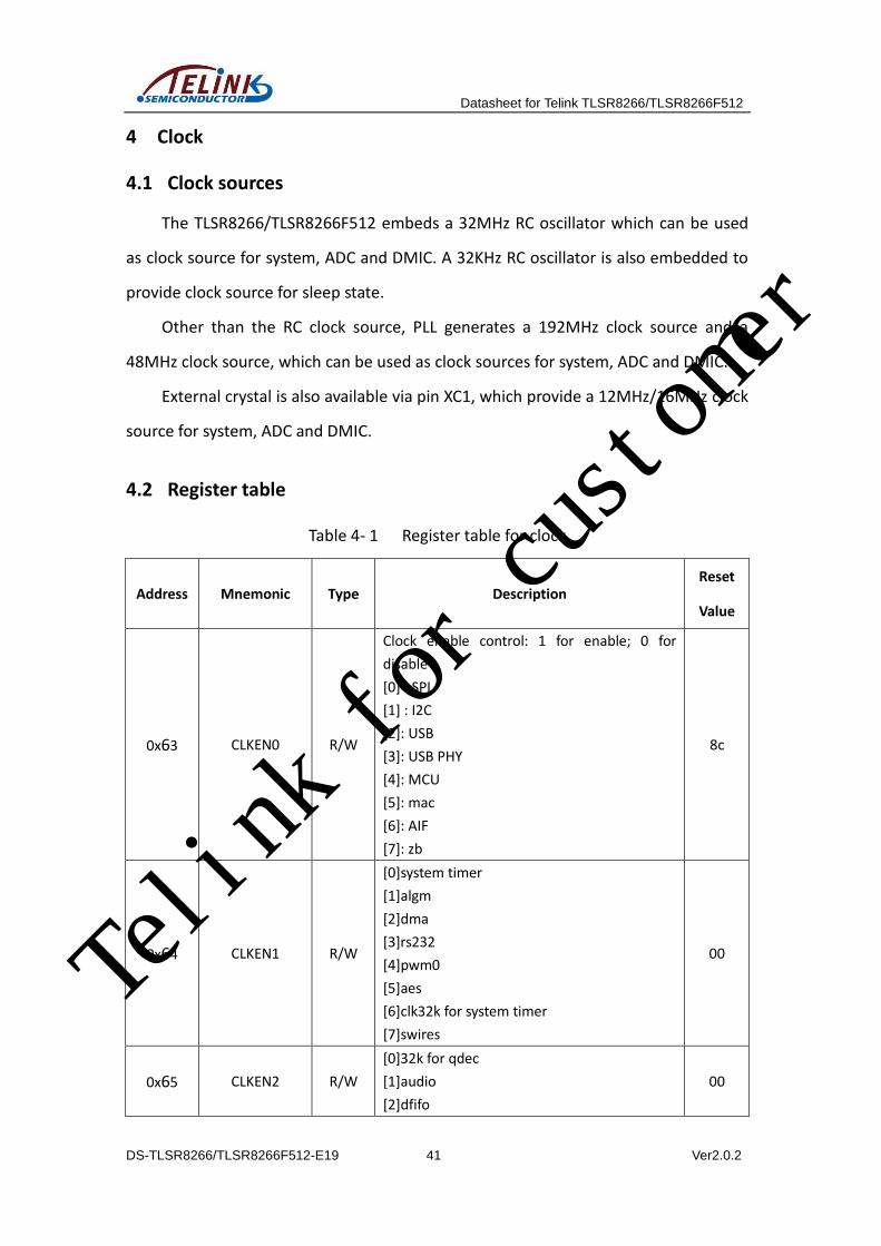
Datasheet for Telink TLSR8266/TLSR8266F512
DS-TLSR8266/TLSR8266F512-E19 41 Ver2.0.2
4 Clock
4.1 Clock sources
The TLSR8266/TLSR8266F512 embeds a 32MHz RC oscillator which can be used
as clock source for system, ADC and DMIC. A 32KHz RC oscillator is also embedded to
provide clock source for sleep state.
Other than the RC clock source, PLL generates a 192MHz clock source and a
48MHz clock source, which can be used as clock sources for system, ADC and DMIC.
External crystal is also available via pin XC1, which provide a 12MHz/16MHz clock
source for system, ADC and DMIC.
4.2 Register table
Table 4- 1 Register table for clock
Address Mnemonic Type Description Reset
Value
0x63 CLKEN0 R/W
Clock enable control: 1 for enable; 0 for
disable
[0] : SPI
[1] : I2C
[2]: USB
[3]: USB PHY
[4]: MCU
[5]: mac
[6]: AIF
[7]: zb
8c
0x64 CLKEN1 R/W
[0]system timer
[1]algm
[2]dma
[3]rs232
[4]pwm0
[5]aes
[6]clk32k for system timer
[7]swires
00
0x65 CLKEN2 R/W
[0]32k for qdec
[1]audio
[2]dfifo
00
Telink for customer

Datasheet for Telink TLSR8266/TLSR8266F512
DS-TLSR8266/TLSR8266F512-E19 42 Ver2.0.2
Address Mnemonic Type Description Reset
Value
[3]key scan
[4]mcic
[5]qdec
[6]32k for pwm
[7]32k for keyscan
0x66 CLKSEL R/W
System clock select
[4:0]: system clock divider:
fhs/((CLKSEL[4:0]+1)).
Fhs refer 0x70 FHS_sel
[6:5]
2’b00:32m clock from rc
2’b01:hs divider clk
2’b10:16M clock from pad
2’b11:32k clk from pad
{0x70[0], 0x66[7]}: FHS sel
ff
0x67 I2S step R/W Reserved 33
0x68 I2S Mod R/W Reserved 2
0x69 Adc step[7:0] R/W ADC clock step[7:0] 00
0x6a Adc mod[7:0] R/W Adc clock mod[7:0] 2
0x6b adcmodstep R/W
[7]: adc clock enable
[6:4] :adc step[10:8]
[3:0] adc mod[11:8]
Adc clock = fhs * step[10:0]/mod[11:0]
Mod need be larger than or equal to 2*step
Fhs refer 0x70 FHS_sel
00
0x6c DMIC_step R/W [7]:digital mic clock enable
[6:0] step 1
0x6d DMIC_mod R/W
[7:0] mod
DMIC clock =fhs*DMIC_step[6:0]/DMIC_mod
Mod need be larger than or equal to 2*step
Fhs refer 0x70 FHS_sel
2
0x70 FHS_sel R/W
{0x70[0], 0x66[7]}: fhs select
2’b00: 192M clock from pll
2’b01:48M pll
2’b10:32M clock from osc
2’b11:16M clock from pad
00
0x71 DC/DC clk mod R/W Reserved
0x73 Clk mux sel
[0]: clk32k select;0:sel 32k osc 1: 32k pad [1]dmic clock select, 1:select 32k (refer bit[0] to decide which 32k ; 0:dmic clk div [2] usb phy clock select,1 : 192M divider
Telink for customer

Datasheet for Telink TLSR8266/TLSR8266F512
DS-TLSR8266/TLSR8266F512-E19 43 Ver2.0.2
Address Mnemonic Type Description Reset
Value
0:48M pll [7:4] r_lpr_div, decide system clock speed in low power mode
4.3 System clock
Rc 32MRC Oscillator
Pad 12M/16MCrystal Oscillator
Pad 32.768KHzCrystal Oscillator
FHS
divider hs divider clk
{0x70[0], 0x66[7]}
00
10
11
0x66[4:0]
sys_clk
System Clock M
UX
01
0x66[6:5]
/4 48M
192M
RC_32MRC Oscillator
Pad_12M/16MCrystal Oscillator
PLL
FHS MUX
00
10
11
01
Figure 4- 1 Block diagram of system clock
There are four selectable clock sources for MCU system clock: 32MHz RC clock,
HS divider clock (divided from a High speed clock), and Pad clock (12MHz/16MHz,
Telink for customer

Datasheet for Telink TLSR8266/TLSR8266F512
DS-TLSR8266/TLSR8266F512-E19 44 Ver2.0.2
32.768KHz).
The high speed clock (FHS) is selectable via address {0x70[0], 0x66[7]} from the
following sources: 192MHz clock from PLL, 48MHz clock from PLL, 32MHz RC clock,
and 12MHz/16MHz Pad clock.
Register CLKSEL (address 0x66) serves to set system clock. System clock source is
selectable via bit[6:5]. If address 0x66[6:5] is set to 2b’01 to select the HS divider clock,
system clock frequency is adjustable via address 0x66[4:0]. FSystem clock = FFHS / (system
clock divider value in address 0x66[4:0] + 1).
4.4 Module clock
Registers CLKEN0~CLKEN2 (address 0x63~0x65) are used to enable or disable
clock for various modules. By disable the clocks of unused modules, current
consumption could be reduced.
4.4.1 ADC clock
ADC clock derives from FHS. ADC clock is enabled via setting address 0x6b[7] to
1b’1.
ADC clock frequency dividing factor contains step and mod. Address 0x6b[6:4]
and 0x69 serve to set ADC clock step[10:0]. Address 0x6b[3:0] and 0x6a serve to set
ADC clock mod[11:0].
ADC clock frequency, FADC clock, equals to FFHS* step[10:0] / mod[11:0].
4.4.2 DMIC clock
Address 0x6c[7] serves to enable DMIC clock.
DMIC clock pin can select 32KHz clock or derive from FHS. Address 0x73 serves to
select DMIC clock source.
In normal DMIC working mode 0x73[1] needs to be set to 1b’0, DMIC clock
divider is selected and frequency dividing factor should be further configured. DMIC
clock frequency dividing factor contains step and mod. Address 0x6c[6:0] serves to set
DMIC clock step[6:0], while address 0x6d serves set DMIC clock mod. In this situation,
Telink for customer

Datasheet for Telink TLSR8266/TLSR8266F512
DS-TLSR8266/TLSR8266F512-E19 45 Ver2.0.2
DMIC clock frequency, FDMIC clock, equals to FFHS* step[6:0] / mod[7:0].
When DMIC is not used, and a 32Khz clock is needed, bit[1] of 0x73 is set to 1b’1
to select the 32KHz clock. bit[0] can be configured to select 32KHz RC oscillator or
32.768KHz Pad clock.
Telink for customer

Datasheet for Telink TLSR8266/TLSR8266F512
DS-TLSR8266/TLSR8266F512-E19 46 Ver2.0.2
5 Timers
5.1 Timer0~Timer2
The TLSR8266/TLSR8266F512 supports three timers: Timer0~ Timer2. The three
timers all support four modes: Mode 0 (System Clock Mode), Mode 1 (GPIO Trigger
Mode), Mode 2 (GPIO Pulse Width Mode) and Mode 3 (Tick Mode).
Timer 2 can also be configured as “watchdog” to monitor firmware running.
5.1.1 Register table
Table 5- 1 Register configuration for Timer0~Timer2
Address Mnemonic Type Description Reset
Value
0x620 TMR_CTRL0 RW
[0]Timer0 enable
[2:1] Timer0 mode.
0 using sclk, 1, using gpio,
2 count widht of gpi, 3 tick
[3]Timer1 enable
[5:4] Timer1 mode.
[6]Timer2 enable
[7]Bit of timer2 mode
00
0x621 TMR_CTRL1 RW [0]Bit of timer2 mode
[7:1]Low bits of watch dog capture 00
0x622 TMR_CTRL2 RW
[6:0]High bits of watch dog capture.
It is compared with [31:18] of
timer2 ticker
[7]watch dog capture
00
0x623 TMR_STATUS RW
[0] timer0 status, write 1 to clear
[1] timer1 status, write 1 to clear
[2] timer2 status, write 1 to clear
[3] watch dog status, write 1 to clear
0x624 TMR_CAPT0_0 RW Byte 0 of timer0 capture 00
Telink for customer

Datasheet for Telink TLSR8266/TLSR8266F512
DS-TLSR8266/TLSR8266F512-E19 47 Ver2.0.2
Address Mnemonic Type Description Reset
Value
0x625 TMR_CAPT0_1 RW Byte 1 of timer0 capture 00
0x626 TMR_CAPT0_2 RW Byte 2 of timer0 capture 00
0x627 TMR_CAPT0_3 RW Byte 3 of timer0 capture 00
0x628 TMR_CAPT1_0 RW Byte 0 of timer1 capture 00
0x629 TMR_CAPT1_1 RW Byte 1 of timer1 capture 00
0x62a TMR_CAPT1_2 RW Byte 2 of timer1 capture 00
0x62b TMR_CAPT1_3 RW Byte 3 of timer1 capture 00
0x62c TMR_CAPT2_0 RW Byte 0 of timer2 capture 00
0x62d TMR_CAPT2_1 RW Byte 1 of timer2 capture 00
0x62e TMR_CAPT2_2 RW Byte 2 of timer2 capture 00
0x62f TMR_CAPT2_3 RW Byte 3 of timer2 capture 00
0x630 TMR_TICK0_0 RW Byte 0 of timer0 ticker
0x631 TMR_TICK0_1 RW Byte 1 of timer0 ticker
0x632 TMR_TICK0_2 RW Byte 2 of timer0 ticker
0x633 TMR_TICK0_3 RW Byte 3 of timer0 ticker
0x634 TMR_TICK1_0 RW Byte 0 of timer1 ticker
0x635 TMR_TICK1_1 RW Byte 1 of timer1 ticker
0x636 TMR_TICK1_2 RW Byte 2 of timer1 ticker
0x637 TMR_TICK1_3 RW Byte 3 of timer1 ticker
0x638 TMR_TICK2_0 RW Byte 0 of timer2 ticker
0x639 TMR_TICK2_1 RW Byte 1 of timer2 ticker
0x63a TMR_TICK2_2 RW Byte 2 of timer2 ticker
0x63b TMR_TICK2_3 RW Byte 3 of timer2 ticker
Telink for customer

Datasheet for Telink TLSR8266/TLSR8266F512
DS-TLSR8266/TLSR8266F512-E19 48 Ver2.0.2
5.1.2 Mode0 (System Clock Mode)
In Mode 0, system clock is employed as clock source.
After Timer is enabled, Timer Tick (i.e. counting value) is increased by 1 on each
positive edge of system clock from preset initial Tick value. Generally the initial Tick
value is set to 0.
Once current Timer Tick value matches the preset Timer Capture (i.e. timing
value), an interrupt is generated, Timer stops counting and Timer status is updated.
Steps of setting Timer0 for Mode 0 is taken as an example.
1st: Set initial Tick value of Timer0
Set Initial value of Tick via registers TMR_TICK0_0~TMR_TICK0_3 (address
0x630~0x633). Address 0x630 is lowest byte and 0x633 is highest byte. It’s
recommended to clear initial Timer Tick value to 0.
2nd: Set Capture value of Timer0
Set registers TMR_CAPT0_0~TMR_CAPT0_3 (address 0x624~0x627). Address
0x624 is lowest byte and 0x627 is highest byte.
3rd: Set Timer0 to Mode 0 and enable Timer0
Set register TMR_CTRL0 (address 0x620) [2:1] to 2b’00 to select Mode 0;
Meanwhile set address 0x620[0] to 1b’1 to enable Timer0. Timer0 starts counting
upward, and Tick value is increased by 1 on each positive edge of system clock until it
reaches Timer0 Capture value.
5.1.3 Mode1 (GPIO Trigger Mode)
In Mode 1, GPIO is employed as clock source. The “m0”/“m1”/“m2” register
specifies the GPIO which generates counting signal for Timer0/Timer1/Timer2.
After Timer is enabled, Timer Tick (i.e. counting value) is increased by 1 on each
positive/negative (configurable) edge of GPIO from preset initial Tick value. Generally
the initial Tick value is set to 0. The “Polarity” register specifies the GPIO edge when
Timer Tick counting increases.
Note: Refer to Section 7.1.2 for corresponding “m0”, “m1”, “m2” and “Polarity”
register address.
Telink for customer

Datasheet for Telink TLSR8266/TLSR8266F512
DS-TLSR8266/TLSR8266F512-E19 49 Ver2.0.2
Once current Timer Tick value matches the preset Timer Capture (i.e. timing
value), an interrupt is generated and timer stops counting.
Steps of setting Timer1 for Mode 1 is taken as an example.
1st: Set initial Tick value of Timer1
Set Initial value of Tick via registers TMR_TICK1_0~TMR_TICK1_3 (address
0x634~0x637). Address 0x634 is lowest byte and 0x637 is highest byte. It’s
recommended to clear initial Timer Tick value to 0.
2nd: Set Capture value of Timer1
Set registers TMR_CAPT1_0~TMR_CAPT1_3 (address 0x628~0x62b). Address
0x628 is lowest byte and 0x62b is highest byte.
3rd: Select GPIO source and edge for Timer1
Select certain GPIO to be the clock source via setting “m1” register.
Select positive edge or negative edge of GPIO input to trigger Timer1 Tick
increment via setting “Polarity” register.
4th: Set Timer1 to Mode 1 and enable Timer1
Set address 0x620[5:4] to 2b’01 to select Mode 1; Meanwhile set address
0x620[3] to 1b’1 to enable Timer1. Timer1 starts counting upward, and Timer1 Tick
value is increased by 1 on each positive/negative (specified during the 3rd step) edge
of GPIO until it reaches Timer1 Capture value.
5.1.4 Mode2 (GPIO Pulse Width Mode)
In Mode 2, system clock is employed as the unit to measure the width of GPIO
pulse. The “m0”/“m1”/“m2” register specifies the GPIO which generates control
signal for Timer0/Timer1/Timer2.
After Timer is enabled, Timer Tick is triggered by a positive/negative
(configurable) edge of GPIO pulse. Then Timer Tick (i.e. counting value) is increased by
1 on each positive edge of system clock from preset initial Tick value. Generally the
initial Tick value is set to 0. The “Polarity” register specifies the GPIO edge when
Timer Tick starts counting.
Note: Refer to Section 7.1.2 for corresponding “m0”, “m1”, “m2” and “Polarity”
Telink for customer

Datasheet for Telink TLSR8266/TLSR8266F512
DS-TLSR8266/TLSR8266F512-E19 50 Ver2.0.2
register address.
While a negative/positive edge of GPIO pulse is detected, an interrupt is
generated and timer stops counting. The GPIO pulse width could be calculated in
terms of tick count and period of system clock.
Steps of setting Timer2 for Mode 2 is taken as an example.
1st: Set initial Timer2 Tick value
Set Initial value of Tick via registers TMR_TICK2_0~TMR_TICK2_3 (address
0x638~0x63b). Address 0x638 is lowest byte and 0x63b is highest byte. It’s
recommended to clear initial Timer Tick value to 0.
2nd: Select GPIO source and edge for Timer2
Select certain GPIO to be the clock source via setting “m2” register.
Select positive edge or negative edge of GPIO input to trigger Timer2 counting
start via setting “Polarity” register.
3rd: Set Timer2 to Mode 2 and enable Timer2
Set address 0x620[7:6] to 2b’01 and address 0x621 [0] to 1b’1.
Timer2 Tick is triggered by a positive/negative (specified during the 2nd step)
edge of GPIO pulse. Timer2 starts counting upward and Timer2 Tick value is increased
by 1 on each positive edge of system clock.
While a negative/positive edge of GPIO pulse is detected, an interrupt is
generated and Timer2 tick stops.
4th: Read current Timer2 Tick value to calculate GPIO pulse width
Read current Timer2 Tick value from address 0x638~0x63b.
Then GPIO pulse width is calculated as follows:
GPIO pulse width
= System clock period ∗ (current Timer2 Tick − intial Timer2 Tick)
For initial Timer2 Tick value set to the recommended value of 0, then:
GPIO pulse width = System clock period ∗ current Timer2 Tick.
5.1.5 Mode3 (Tick Mode)
In Mode 3, system clock is employed.
Telink for customer

Datasheet for Telink TLSR8266/TLSR8266F512
DS-TLSR8266/TLSR8266F512-E19 51 Ver2.0.2
After Timer is enabled, Timer Tick starts counting upward, and Timer Tick value is
increased by 1 on each positive edge of system clock.
This mode could be used as time indicator. There will be no interrupt generated.
Timer Tick keeps rolling from 0 to 0xffffffff. When Timer tick overflows, it returns to 0
and starts counting upward again.
Steps of setting Timer0 for Mode 3 is taken as an example.
1st: Set initial Tick value of Timer0
Set Initial value of Tick via address 0x630~0x633. Address 0x630 is lowest byte
and address 0x633 is highest byte. It’s recommended to clear initial Timer Tick value
to 0.
2nd: Set Timer0 to Mode 3 and enable Timer0
Set address 0x620[2:1] to 2b’11 to select Mode 3, meanwhile set address
0x620[0] to 1b’1 to enable Timer0. Timer0 Tick starts to roll.
3rd: Read current Timer0 Tick value
Current Timer0 Tick value can be read from address 0x630~0x633.
5.1.6 Watchdog
Programmable watchdog could reset chip from unexpected hang up or
malfunction.
Only Timer2 supports Watchdog.
Timer2 Tick has 32bits. Watchdog Capture has only 14bits, which consists of
TMR_CTRL2 (address 0x622) [6:0] as higher bits and TMR_CTRL1 (address 0x621) [7:1]
as lower bits. Chip will be reset when the Timer2 Tick[31:18] matches Watch dog
capture.
1st: Clear Timer2 Tick value
Clear registers TMR_TICK2_0 ~TMR_TICK2_3 (address 0x638~0x63b). Address
0x638 is lowest byte and 0x63b is highest byte.
2nd: Enable Timer2
Set register TMR_CTRL0 (address 0x620) [6] to 1b’1 to enable Timer2.
3rd: Set 14-bit Watchdog Capture value and enable Watchdog
Telink for customer

Datasheet for Telink TLSR8266/TLSR8266F512
DS-TLSR8266/TLSR8266F512-E19 52 Ver2.0.2
Set address 0x622[6:0] as higher bits of watchdog capture and 0x621[7:1] as
lower bits. Meanwhile set address 0x622[7] to 1b’1 to enable Watchdog.
Then Timer2 Tick starts counting upwards from 0.
If bits[31:18] of Timer2 Tick value read from address 0x638~0x63b reaches
watchdog capture, the chip will be reset.
5.2 32K LTIMER
The TLSR8266/TLSR8266F512 supports a low frequency (32KHz) LTIMER in
suspend mode or deep sleep mode.
This timer can be used as one kind of wakeup source. Please refer to Section
2.5.2 for details.
5.3 System Timer
The TLSR8266/TLSR8266F512 also supports a System Timer.
In suspend mode, both System Timer and Timer0~Timer2 stop counting, and 32K
Timer starts counting. When the chip restores to active mode, Timer0~Timer2 will
continue counting from the number when they stops; In contrast, System Timer will
continue counting from an adjusted number which is a sum of the number when it
stops and an offset calculated from the counting value of 32K Timer during suspend
mode.
Telink for customer
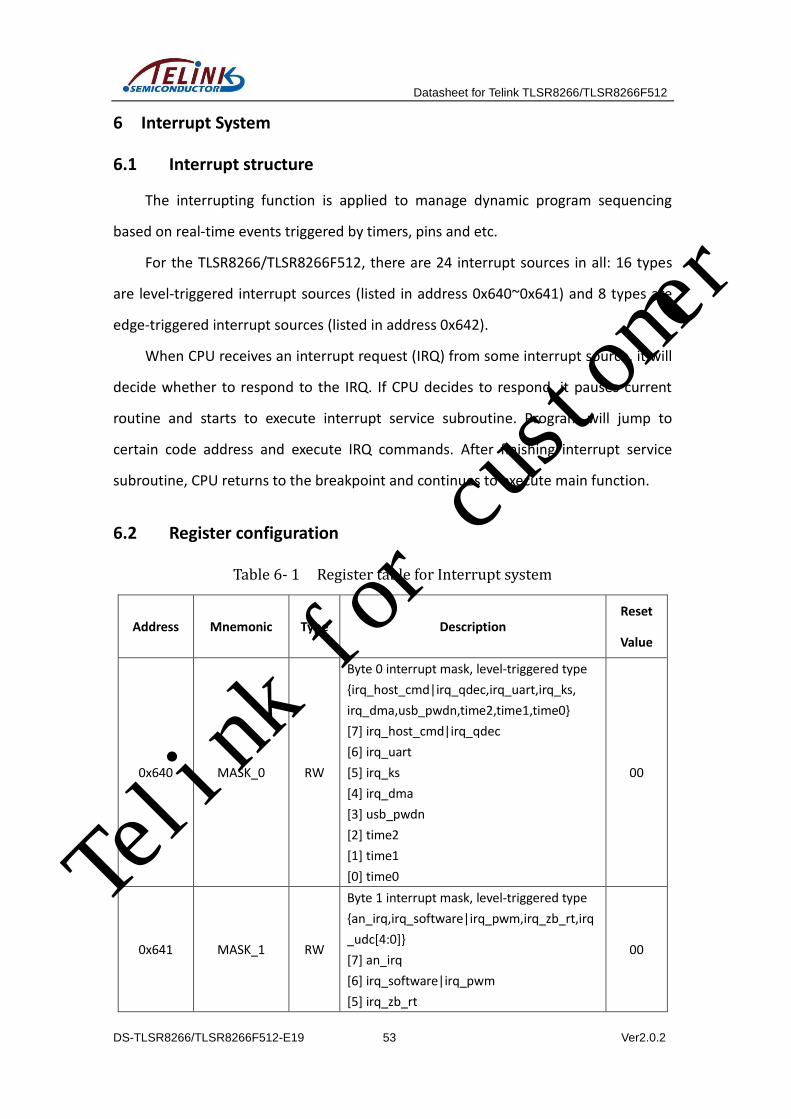
Datasheet for Telink TLSR8266/TLSR8266F512
DS-TLSR8266/TLSR8266F512-E19 53 Ver2.0.2
6 Interrupt System
6.1 Interrupt structure
The interrupting function is applied to manage dynamic program sequencing
based on real-time events triggered by timers, pins and etc.
For the TLSR8266/TLSR8266F512, there are 24 interrupt sources in all: 16 types
are level-triggered interrupt sources (listed in address 0x640~0x641) and 8 types are
edge-triggered interrupt sources (listed in address 0x642).
When CPU receives an interrupt request (IRQ) from some interrupt source, it will
decide whether to respond to the IRQ. If CPU decides to respond, it pauses current
routine and starts to execute interrupt service subroutine. Program will jump to
certain code address and execute IRQ commands. After finishing interrupt service
subroutine, CPU returns to the breakpoint and continues to execute main function.
6.2 Register configuration
Table 6- 1 Register table for Interrupt system
Address Mnemonic Type Description Reset
Value
0x640 MASK_0 RW
Byte 0 interrupt mask, level-triggered type
{irq_host_cmd|irq_qdec,irq_uart,irq_ks,
irq_dma,usb_pwdn,time2,time1,time0}
[7] irq_host_cmd|irq_qdec
[6] irq_uart
[5] irq_ks
[4] irq_dma
[3] usb_pwdn
[2] time2
[1] time1
[0] time0
00
0x641 MASK_1 RW
Byte 1 interrupt mask, level-triggered type
{an_irq,irq_software|irq_pwm,irq_zb_rt,irq
_udc[4:0]}
[7] an_irq
[6] irq_software|irq_pwm
[5] irq_zb_rt
00
Telink for customer

Datasheet for Telink TLSR8266/TLSR8266F512
DS-TLSR8266/TLSR8266F512-E19 54 Ver2.0.2
Address Mnemonic Type Description Reset
Value
[4] irq_udc[4]
[3] irq_udc[3]
[2] irq_udc[2]
[1] irq_udc[1]
[0] irq_udc[0]
0x642 MASK_2 RW
Byte 2 interrupt mask, edge-triggered type
{gpio2risc[2:0],irq_stimer,pm_irq,irq_gpio,u
sb_reset,usb_250us}
[7] gpio2risc[2]
[6] gpio2risc[1]
[5] gpio2risc[0]
[4] irq_stimer
[3] pm_irq
[2] irq_gpio
[1] usb_reset
[0] usb_250us
00
0x643 IRQMODE RW [0] interrupt enable
[1] reserved (Multi-Address enable) 00
0x644 PRIO_0 RW
Byte 0 of priority
1: High priority;
0: Low priority
00
0x645 PRIO_1 RW Byte 1 of priority 00
0x646 PRIO_2 RW Byte 2 of priority 00
0x648 IRQSRC_0 R Byte 0 of interrupt source
0x649 IRQSRC_1 R Byte 1 of interrupt source
0x64a IRQSRC_2 R Byte 2 of interrupt source
6.2.1 Enable/Mask interrupt sources
Various interrupt sources could be enabled or masked by registers
MASK_0~MASK_2 (address 0x640~0x642).
6.2.2 Interrupt mode and priority
Interrupt mode is typically-used mode. Register IRQMODE (address 0x643)[0]
should be set to 1b’1 to enable interrupt function.
IRQ tasks could be set as High or Low priority via registers PRIO_0~PRIO_2
(address 0x644~0x646). When more than one interrupt sources assert interrupt
Telink for customer

Datasheet for Telink TLSR8266/TLSR8266F512
DS-TLSR8266/TLSR8266F512-E19 55 Ver2.0.2
requests at the same time, CPU will respond depending on respective interrupt
priority levels. It’s recommended not to modify priority setting.
6.2.3 Interrupt source flag
Three bytes in registers IRQSRC_0~IRQSRC_2 (address 0x648~0x64a) serve to
indicate IRQ sources. Once IRQ occurs from certain source, the corresponding IRQ
source flag will be raised to “High”. User could identify IRQ source by reading address
0x648~0x64a.
When handling edge-triggered type interrupt, the corresponding IRQ source flag
needs to be cleared via address 0x64a. Take the interrupt source usb_250us for
example: First enable the interrupt source by setting address 0x642 bit[0] to 1; then
set address 0x643 bit[0] to 1 to enable the interrupt. In interrupt handling function,
24-bit data is read from address 0x648~0x64a to determine which IRQ source is valid;
if data bit[16] is 1, it means the usb_250us interrupt is valid. Clear this interrupt
source by setting address 0x64a bit[0] to 1.
As for level-type interrupt, IRQ interrupt source status needs to be cleared via
setting corresponding module status register. Take Timer0 IRQ interrupt source for
example, register TMR_STATUS (address 0x623) [0] should be written with 1b’1 to
clear Timer0 status (refer to section 5.1.1).
Telink for customer

Datasheet for Telink TLSR8266/TLSR8266F512
DS-TLSR8266/TLSR8266F512-E19 56 Ver2.0.2
7 Interface
7.1 GPIO
The TLSR8266ET/AT56, TLSR8266ET/AT48, TLSR8266ET/AT32,
TLSR8266F512ET/AT48 and TLSR8266F512ET/AT32 support up to 41, 37, 22, 35 and 20
GPIOs respectively. Except for dedicated GPIOs, all digital IOs can be used as general
purpose IOs. All GPIOs have configurable pull-up/pull-down resistor. Note: For GPIO
function, the USB interface (DM, DP) can only be used as GPI.
7.1.1 Basic configuration
Please refer to Table 7-1 in section 7.1.1.3 for various GPIO interface
configuration.
7.1.1.1 Multiplexed functions
For a pin listed in Table 7-1, it acts as the function in the “Default Function”
column by default. It’s noted that functions of higher priority should be disabled (by
clearing corresponding bit) before enabling function of lower priority (by setting
corresponding bit to 1b’1).
If a pin with multiplexed functions does not act as GPIO function by default, to
use it as GPIO function, first set the bit in “Act as GPIO” column to 1b’1. After GPIO
function is enabled, if the pin is used as output, both the bits in “IE” and “OEN”
columns should be cleared, then set the register value in the “Output” column; if the
pin is used as input, both the bits in “IE” and “OEN” columns set to 1b’1, and the input
data can be read from the register in the “Input” column.
Take the PWM3/ANA_A<1> pin for example.
(1) The pin acts as GPIO function by default. If the pin is used as general output,
both address 0x581[1] and 0x582[1] should be cleared, then configure
address 0x583[1]. If the pin is used as general input, both address 0x581[1]
and 0x582[1] should be set to 1b’1, and the input data can be read from
address 0x580[1].
(2) To use the pin as Keyscan function, address 0x586[1] should be cleared and
Telink for customer

Datasheet for Telink TLSR8266/TLSR8266F512
DS-TLSR8266/TLSR8266F512-E19 57 Ver2.0.2
0x5b0[1] should be set to 1b’1.
(3) Addresses {0x586[1], 0x5b0[1], 0x5b6[4]} should be all cleared to use the pin
as PWM3 function.
Take the SWS/ANA_A<0> pin as another example. The pin acts as SWS function
by default. To use it as GPIO function, first set address 0x586[0] to 1b’1. If the pin is
used as general output, both address 0x581[0] and 0x582[0] should be cleared, then
configure address 0x583[0]. If the pin is used as general input, both address 0x581[0]
and 0x582[0] should be set to 1b’1, and the input data can be read from address
0x580[0].
7.1.1.2 Drive strength
The registers in the “DS” column are used to configure corresponding pin’s
driving strength: “1” indicates maximum drive level, while “0” indicates minimal drive
level. The “DS” configuration will take effect when the pin is used as output. It’s set as
the strongest driving level by default. In actual applications, driving strength can be
decreased to lower level if necessary.
All the pins support maximum drive level of 4mA (“DS”=1) and minimal drive
level of 0.7mA (“DS”=0) with the following exceptions:
ANA_B<6> and ANA_B<5>: maximum=8mA (“DS”=1), minimum=4mA (“DS”=0)
ANA_E<5> and ANA_E<4>: maximum=16mA (“DS”=1), minimum=12mA (“DS”=0)
7.1.1.3 GPIO lookup table
Table 7- 1 GPIO lookup table
Pin
Default
Function
Prio_0 Prio_1 Prio_2 Prio_3 Prio_4
GPIO setting
Input
(R)
IE
(High
active)
OEN
(Low
active)
Output DS
Act as
GPIO
SWS/
ANA_A<0> SWS 0x580[0] 0x581[0] 0x582[0] 0x583[0] 0x585[0] 0x586[0]
PWM3/ GPIO 5b0[1] 5b6[4] 0x580[1] 0x581[1] 0x582[1] 0x583[1] 0x585[1] 0x586[1]
Telink for customer

Datasheet for Telink TLSR8266/TLSR8266F512
DS-TLSR8266/TLSR8266F512-E19 58 Ver2.0.2
Pin
Default
Function
Prio_0 Prio_1 Prio_2 Prio_3 Prio_4
GPIO setting
Input
(R)
IE
(High
active)
OEN
(Low
active)
Output DS
Act as
GPIO
ANA_A<1> ks bb_dbg[0]
MSDI/
ANA_A<2> MSDI 0x580[2] 0x581[2] 0x582[2] 0x583[2] 0x585[2] 0x586[2]
MCLK/
ANA_A<3> MCLK 0x580[3] 0x581[3] 0x582[3] 0x583[3] 0x585[3] 0x586[3]
GP18/
PWM3_N/
ANA_A<4>
GPIO 5b0[4]
ks
5b6[4]
bb_dbg[1] 0x580[4] 0x581[4] 0x582[4] 0x583[4] 0x585[4] 0x586[4]
PWM4/
ANA_A<5> GPIO
5b0[5]
ks
5b6[4]
bb_dbg[2] 0x580[5] 0x581[5] 0x582[5] 0x583[5] 0x585[5] 0x586[5]
GP19/
PWM4_N/
ANA_A<6>
GPIO 5b0[6]
ks
5b6[4]
bb_dbg[3] 0x580[6] 0x581[6] 0x582[6] 0x583[6] 0x585[6] 0x586[6]
SWM/
ANA_A<7> GPIO
5b0[7]
ks 0x580[7] 0x581[7] 0x582[7] 0x583[7] 0x585[7] 0x586[7]
PWM5/
ANA_B<0> GPIO
5b6[0]
rxadc_clk_i
5b6[8]
rxadc_clk_o 0x588[0] 0x589[0] 0x58a[0] 0x58b[0] 0x58d[0] 0x58e[0]
GP20/
PWM5_N/
ANA_B<1>
GPIO 5b6[0]
rxadc_dat_i
5b6[8]
rxadc_dat_
o
0x588[1] 0x589[1] 0x58a[1] 0x58b[1] 0x58d[1] 0x58e[1]
MSDO/
ANA_B<2> MSDO 0x588[2] 0x589[2] 0x58a[2] 0x58b[2] 0x58d[2] 0x58e[2]
MSCN/
ANA_B<3> MSCN 0x588[3] 0x589[3] 0x58a[3] 0x58b[3] 0x58d[3] 0x58e[3]
DM/
ANA_B<5> DM 0x588[5] 0x589[5] N/A N/A 0x58d[5] N/A
DP/
ANA_B<6> DP 0x588[6] 0x589[6] N/A N/A 0x58d[6] N/A
GP0/
PWM0_N/
ANA_B<7>
GPIO 0x588[7] 0x589[7] 0x58a[7] 0x58b[7] 0x58d[7] 0x58e[7]
PWM0/
ANA_C<0>/
Amic_Bias
GPIO 5b2[0]
ks
5b6[6]
tx_en_i
5b6[7]
tx_en_o 0x590[0] 0x591[0] 0x592[0] 0x593[0] 0x595[0] 0x596[0]
GP1/
PWM1_N/
ANA_C<1>/
GPIO 5b2[1]
ks
5b6[6]
tx_cyc1_i
5b6[7]
tx_cyc1_o 0x590[1] 0x591[1] 0x592[1] 0x593[1] 0x595[1] 0x596[1]
Telink for customer

Datasheet for Telink TLSR8266/TLSR8266F512
DS-TLSR8266/TLSR8266F512-E19 59 Ver2.0.2
Pin
Default
Function
Prio_0 Prio_1 Prio_2 Prio_3 Prio_4
GPIO setting
Input
(R)
IE
(High
active)
OEN
(Low
active)
Output DS
Act as
GPIO
Amic_In
PWM1_N/
ANA_C<2> GPIO
5b2[2]
ks 0x590[2] 0x591[2] 0x592[2] 0x593[2] 0x595[2] 0x596[2]
GP2/
PMW1/
ANA_C<3>
GPIO 5b2[3]
ks
5b6[6]
tx_sd_i
5b6[7]
tx_sd_o 0x590[3] 0x591[3] 0x592[3] 0x593[3] 0x595[3] 0x596[3]
PWM2/
ANA_C<4> GPIO
5b2[4]
ks
5b6[6]
tx_clkbb_i
5b6[7]
tx_clkbb_o 0x590[4] 0x591[4] 0x592[4] 0x593[4] 0x595[4] 0x596[4]
GP3/
PWM2_N/
ANA_C<5>
GPIO 5b2[5]
ks
5b6[4]
bb_dbg[4] 0x590[5] 0x591[5] 0x592[5] 0x593[5] 0x595[5] 0x596[5]
GP4/
uart_tx/
ANA_C<6>
GPIO 5b2[6]
ks 0x590[6] 0x591[6] 0x592[6] 0x593[6] 0x595[6] 0x596[6]
GP5/
uart_rx/
ANA_C<7>
GPIO 5b2[7]
ks 0x590[7] 0x591[7] 0x592[7] 0x593[7] 0x595[7] 0x596[7]
GP6/
uart_rts/
ANA_D<0>
GPIO 5b3[0]
ks uart_rts 0x598[0] 0x599[0] 0x59a[0] 0x59b[0] 0x59d[0] 0x59e[0]
GP7/
uart_cts/
ANA_D<1>
GPIO 5b3[1]
ks
5b6[1]
uart_cts 0x598[1] 0x599[1] 0x59a[1] 0x59b[1] 0x59d[1] 0x59e[1]
GP8/
PWM3/
ANA_D<2>
GPIO 5b3[2]
ks
5b6[4]
bb_dbg[5] 0x598[2] 0x599[2] 0x59a[2] 0x59b[2] 0x59d[2] 0x59e[2]
GP9/
PWM4/
ANA_D<3>
GPIO 5b3[3]
ks
5b6[4]
bb_dbg[6] 0x598[3] 0x599[3] 0x59a[3] 0x59b[3] 0x59d[3] 0x59e[3]
GP10/
ANA_D<4> GPIO
5b3[4]
ks
5b6[4]
bb_dbg[7] 0x598[4] 0x599[4] 0x59a[4] 0x59b[4] 0x59d[4] 0x59e[4]
GP11/
ANA_D<5> GPIO
5b3[5]
ks
5b6[4]
bb_dbg[8] 0x598[5] 0x599[5] 0x59a[5] 0x59b[5] 0x59d[5] 0x59e[5]
GP12/
ANA_D<6>/
Rbias_EXT
GPIO 5b3[6]
ks 0x598[6] 0x599[6] 0x59a[6] 0x59b[6] 0x59d[6] 0x59e[6]
GP13/ GPIO 5b3[7] 5b6[4] 0x598[7] 0x599[7] 0x59a[7] 0x59b[7] 0x59d[7] 0x59e[7]
Telink for customer

Datasheet for Telink TLSR8266/TLSR8266F512
DS-TLSR8266/TLSR8266F512-E19 60 Ver2.0.2
Pin
Default
Function
Prio_0 Prio_1 Prio_2 Prio_3 Prio_4
GPIO setting
Input
(R)
IE
(High
active)
OEN
(Low
active)
Output DS
Act as
GPIO
ANA_D<7> ks bb_dbg[9]
GP14/
ANA_E<0> GPIO
5b4[0]
ks
5b6[4]
bb_dbg[10] 0x5a0[0] 0x5a1[0] 0x5a2[0] 0x5a3[0] 0x5a5[0] 0x5a6[0]
DMIC_CK/
ANA_E<1> GPIO
5b4[1]
ks 0x5a0[1] 0x5a1[1] 0x5a2[1] 0x5a3[1] 0x5a5[1] 0x5a6[1]
DMIC_DI/
ANA_E<2> GPIO
5b4[2]
ks 0x5a0[2] 0x5a1[2] 0x5a2[2] 0x5a3[2] 0x5a5[2] 0x5a6[2]
GP15/
ANA_E<3> GPIO
5b4[3]
ks
5b6[4]
bb_dbg[11] 0x5a0[3] 0x5a1[3] 0x5a2[3] 0x5a3[3] 0x5a5[3] 0x5a6[3]
GP16/
SDM_P/
ANA_E<4>
GPIO 5b4[4]
ks
5b6[4]
bb_dbg[12] SDM_P 0x5a0[4] 0x5a1[4] 0x5a2[4] 0x5a3[4] 0x5a5[4] 0x5a6[4]
GP17/
SDM_N/
ANA_E<5>
GPIO 5b4[5]
ks
5b6[4]
bb_dbg[13] SDM_N 0x5a0[5] 0x5a1[5] 0x5a2[5] 0x5a3[5] 0x5a5[5] 0x5a6[5]
CN/
uart_rts/
ANA_E<6>
CN 5b4[6]
ks
5b6[5]
uart_rts 0x5a0[6] 0x5a1[6] 0x5a2[6] 0x5a3[6] 0x5a5[6] 0x5a6[6]
DI/
I2C_SDA/
ANA_E<7>
DI 5b4[7]
ks 0x5a0[7] 0x5a1[7] 0x5a2[7] 0x5a3[7] 0x5a5[7] 0x5a6[7]
DO/
uart_cts/
ANA_F<0>
DO 5b6[5]
uart_cts 0x5a8[0] 0x5a9[0] 0x5aa[0] 0x5ab[0] 0x5ad[0] 0x5ae[0]
CK/
I2C_SCL/
ANA_F<1>
CK 0x5a8[1] 0x5a9[1] 0x5aa[1] 0x5ab[1] 0x5ad[1] 0x5ae[1]
*Notes:
(1) ks: key_scan
(2) Priority: acting as GPIO is the highest priority and prio0 > prio1 > prio2 > prio3 >
prio4.
(3) GPIO acts as input by default except ANA_D<5:4>: ANA_D<4> outputs 1 while
ANA_D<5> outputs 0.
Telink for customer

Datasheet for Telink TLSR8266/TLSR8266F512
DS-TLSR8266/TLSR8266F512-E19 61 Ver2.0.2
7.1.2 Connection relationship between GPIO and related modules
GPIO can be used to generate GPIO interrupt signal for interrupt system, as well
as counting or control signal for Timer/Counter module.
For the “Exclusive Or (XOR)” operation result for input signal from any GPIO pin
and respective “polarity” value, on one hand, it takes “And” operation with “irq” and
generates GPIO interrupt request signal; on the other hand, it takes “And” operation
with “m0/m1/m2” and generates counting signal in Mode 1 or control signal in Mode
2 for Timer0/Timer1/Timer2.
GPIO interrupt request signal = | ((input ^ polarity) & irq);
Counting (Mode 1) or control (Mode 2) signal for Timer0 = | ((input ^ polarity) &
m0);
Counting (Mode 1) or control (Mode 2) signal for Timer1 = | ((input ^ polarity) &
m1);
Counting (Mode 1) or control (Mode 2) signal for Timer2 = | ((input ^ polarity) &
m2);
Timer0
Timer1
Timer2
Input
Polarity
m1
m0
m2
Irq GPIO_IRQ
Timer0_IRQ
Timer1_IRQ
Timer2_IRQ
Figure 7- 1 Logic relationship between GPIO and related modules
Please refer to Table 7-2 to learn how to configure GPIO for interrupt system or
Timer/Counter (Mode 1 or Mode 2).
(1) First enable GPIO function, IE and disable OEN.
Telink for customer

Datasheet for Telink TLSR8266/TLSR8266F512
DS-TLSR8266/TLSR8266F512-E19 62 Ver2.0.2
(2) GPIO IRQ signal: Select GPIO interrupt trigger edge (positive edge or negative
edge) via configuring “Polarity”, and set corresponding GPIO interrupt
enabling bit “Irq”. Then set address 0x5b5[3] to enable GPIO IRQ. Finally
enable GPIO interrupt (address 0x642[2]). User can read addresses 0x5e0 ~
0x5e7 to see which GPIO asserts GPIO interrupt request signal.
(3) Timer/Counter counting or control signal: Configure “Polarity” (In Mode 1, it
determines GPIO edge when Timer Tick counting increases; in Mode 2, it
determines GPIO edge when Timer Tick starts counting) and set “m0/m1/m2”.
User can read addresses 0x5e8~0x5ef/0x5f0~0x5f7/0x5f8~0x5ff to see which
GPIO asserts counting signal (in Mode 1) or control signal (in Mode 2) for
Timer0/Timer1/Timer2.
Table 7- 2 GPIO lookup table2
Pin Input
(R)
Polarity
1: active low
0: active high
Irq m0 m1 m2
SWS/ANA_A<0> 0x580[0] 0x584[0] 0x587[0] 0x5b8[0] 0x5c0[0] 0x5c8[0]
PWM3/ANA_A<1> 0x580[1] 0x584[1] 0x587[1] 0x5b8[1] 0x5c0[1] 0x5c8[1]
MSDI/ANA_A<2> 0x580[2] 0x584[2] 0x587[2] 0x5b8[2] 0x5c0[2] 0x5c8[2]
MCLK/ANA_A<3> 0x580[3] 0x584[3] 0x587[3] 0x5b8[3] 0x5c0[3] 0x5c8[3]
GP18/PWM3_N/ANA_A<4> 0x580[4] 0x584[4] 0x587[4] 0x5b8[4] 0x5c0[4] 0x5c8[4]
PWM4/ANA_A<5> 0x580[5] 0x584[5] 0x587[5] 0x5b8[5] 0x5c0[5] 0x5c8[5]
GP19/PWM4_N/ANA_A<6> 0x580[6] 0x584[6] 0x587[6] 0x5b8[6] 0x5c0[6] 0x5c8[6]
SWM/ANA_A<7> 0x580[7] 0x584[7] 0x587[7] 0x5b8[7] 0x5c0[7] 0x5c8[7]
PWM5/ANA_B<0> 0x588[0] 0x58c[0] 0x58f[0] 0x5b9[0] 0x5c1[0] 0x5c9[0]
GP20/PWM5_N/ANA_B<1> 0x588[1] 0x58c[1] 0x58f[1] 0x5b9[1] 0x5c1[1] 0x5c9[1]
MSDO/ANA_B<2> 0x588[2] 0x58c[2] 0x58f[2] 0x5b9[2] 0x5c1[2] 0x5c9[2]
MSCN/ANA_B<3> 0x588[3] 0x58c[3] 0x58f[3] 0x5b9[3] 0x5c1[3] 0x5c9[3]
DM/ANA_B<5> 0x588[5] 0x58c[5] 0x58f[5] 0x5b9[5] 0x5c1[5] 0x5c9[5]
DP/ANA_B<6> 0x588[6] 0x58c[6] 0x58f[6] 0x5b9[6] 0x5c1[6] 0x5c9[6]
Telink for customer
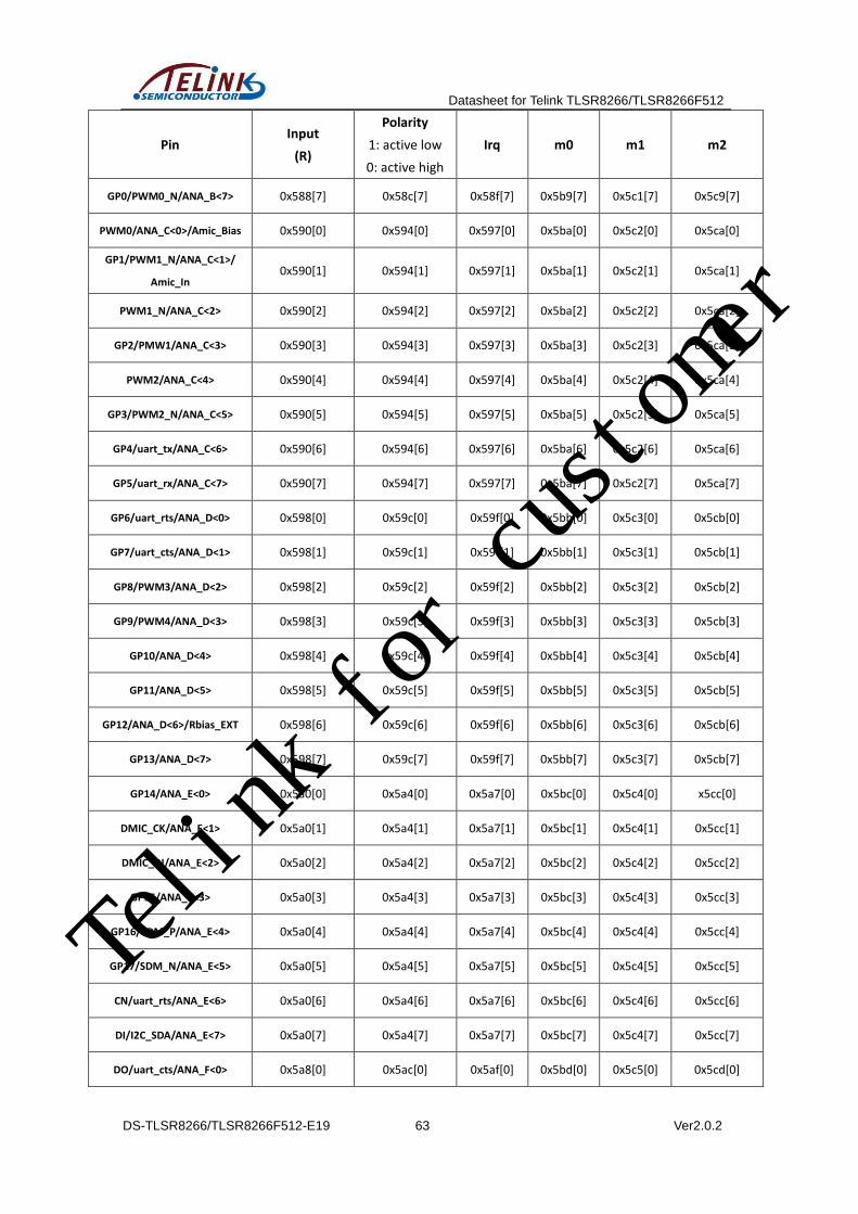
Datasheet for Telink TLSR8266/TLSR8266F512
DS-TLSR8266/TLSR8266F512-E19 63 Ver2.0.2
Pin Input
(R)
Polarity
1: active low
0: active high
Irq m0 m1 m2
GP0/PWM0_N/ANA_B<7> 0x588[7] 0x58c[7] 0x58f[7] 0x5b9[7] 0x5c1[7] 0x5c9[7]
PWM0/ANA_C<0>/Amic_Bias 0x590[0] 0x594[0] 0x597[0] 0x5ba[0] 0x5c2[0] 0x5ca[0]
GP1/PWM1_N/ANA_C<1>/
Amic_In 0x590[1] 0x594[1] 0x597[1] 0x5ba[1] 0x5c2[1] 0x5ca[1]
PWM1_N/ANA_C<2> 0x590[2] 0x594[2] 0x597[2] 0x5ba[2] 0x5c2[2] 0x5ca[2]
GP2/PMW1/ANA_C<3> 0x590[3] 0x594[3] 0x597[3] 0x5ba[3] 0x5c2[3] 0x5ca[3]
PWM2/ANA_C<4> 0x590[4] 0x594[4] 0x597[4] 0x5ba[4] 0x5c2[4] 0x5ca[4]
GP3/PWM2_N/ANA_C<5> 0x590[5] 0x594[5] 0x597[5] 0x5ba[5] 0x5c2[5] 0x5ca[5]
GP4/uart_tx/ANA_C<6> 0x590[6] 0x594[6] 0x597[6] 0x5ba[6] 0x5c2[6] 0x5ca[6]
GP5/uart_rx/ANA_C<7> 0x590[7] 0x594[7] 0x597[7] 0x5ba[7] 0x5c2[7] 0x5ca[7]
GP6/uart_rts/ANA_D<0> 0x598[0] 0x59c[0] 0x59f[0] 0x5bb[0] 0x5c3[0] 0x5cb[0]
GP7/uart_cts/ANA_D<1> 0x598[1] 0x59c[1] 0x59f[1] 0x5bb[1] 0x5c3[1] 0x5cb[1]
GP8/PWM3/ANA_D<2> 0x598[2] 0x59c[2] 0x59f[2] 0x5bb[2] 0x5c3[2] 0x5cb[2]
GP9/PWM4/ANA_D<3> 0x598[3] 0x59c[3] 0x59f[3] 0x5bb[3] 0x5c3[3] 0x5cb[3]
GP10/ANA_D<4> 0x598[4] 0x59c[4] 0x59f[4] 0x5bb[4] 0x5c3[4] 0x5cb[4]
GP11/ANA_D<5> 0x598[5] 0x59c[5] 0x59f[5] 0x5bb[5] 0x5c3[5] 0x5cb[5]
GP12/ANA_D<6>/Rbias_EXT 0x598[6] 0x59c[6] 0x59f[6] 0x5bb[6] 0x5c3[6] 0x5cb[6]
GP13/ANA_D<7> 0x598[7] 0x59c[7] 0x59f[7] 0x5bb[7] 0x5c3[7] 0x5cb[7]
GP14/ANA_E<0> 0x5a0[0] 0x5a4[0] 0x5a7[0] 0x5bc[0] 0x5c4[0] x5cc[0]
DMIC_CK/ANA_E<1> 0x5a0[1] 0x5a4[1] 0x5a7[1] 0x5bc[1] 0x5c4[1] 0x5cc[1]
DMIC_DI/ANA_E<2> 0x5a0[2] 0x5a4[2] 0x5a7[2] 0x5bc[2] 0x5c4[2] 0x5cc[2]
GP15/ANA_E<3> 0x5a0[3] 0x5a4[3] 0x5a7[3] 0x5bc[3] 0x5c4[3] 0x5cc[3]
GP16/SDM_P/ANA_E<4> 0x5a0[4] 0x5a4[4] 0x5a7[4] 0x5bc[4] 0x5c4[4] 0x5cc[4]
GP17/SDM_N/ANA_E<5> 0x5a0[5] 0x5a4[5] 0x5a7[5] 0x5bc[5] 0x5c4[5] 0x5cc[5]
CN/uart_rts/ANA_E<6> 0x5a0[6] 0x5a4[6] 0x5a7[6] 0x5bc[6] 0x5c4[6] 0x5cc[6]
DI/I2C_SDA/ANA_E<7> 0x5a0[7] 0x5a4[7] 0x5a7[7] 0x5bc[7] 0x5c4[7] 0x5cc[7]
DO/uart_cts/ANA_F<0> 0x5a8[0] 0x5ac[0] 0x5af[0] 0x5bd[0] 0x5c5[0] 0x5cd[0]
Telink for customer
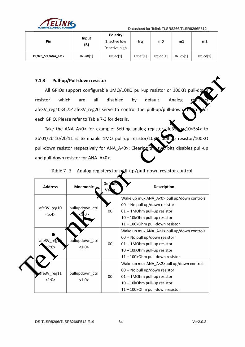
Datasheet for Telink TLSR8266/TLSR8266F512
DS-TLSR8266/TLSR8266F512-E19 64 Ver2.0.2
Pin Input
(R)
Polarity
1: active low
0: active high
Irq m0 m1 m2
CK/I2C_SCL/ANA_F<1> 0x5a8[1] 0x5ac[1] 0x5af[1] 0x5bd[1] 0x5c5[1] 0x5cd[1]
7.1.3 Pull-up/Pull-down resistor
All GPIOs support configurable 1MΩ/10KΩ pull-up resistor or 100KΩ pull-down
resistor which are all disabled by default. Analog registers
afe3V_reg10<4:7>~afe3V_reg20 serve to control the pull-up/pull-down resistor for
each GPIO. Please refer to Table 7-3 for details.
Take the ANA_A<0> for example: Setting analog register afe3V_reg10<5:4> to
2b’01/2b’10/2b’11 is to enable 1MΩ pull-up resistor/10KΩ pull-up resistor/100KΩ
pull-down resistor respectively for ANA_A<0>; Clearing the two bits disables pull-up
and pull-down resistor for ANA_A<0>.
Table 7- 3 Analog registers for pull-up/pull-down resistor control
Address Mnemonic Default
Value Description
afe3V_reg10
<5:4>
pullupdown_ctrl
<1:0> 00
Wake up mux ANA_A<0> pull up/down controls
00 -- No pull up/down resistor
01 -- 1MOhm pull-up resistor
10 – 10kOhm pull-up resistor
11 – 100kOhm pull-down resistor
afe3V_reg10
<7:6>
pullupdown_ctrl
<1:0> 00
Wake up mux ANA_A<1> pull up/down controls
00 -- No pull up/down resistor
01 -- 1MOhm pull-up resistor
10 – 10kOhm pull-up resistor
11 – 100kOhm pull-down resistor
afe3V_reg11
<1:0>
pullupdown_ctrl
<1:0> 00
Wake up mux ANA_A<2>pull up/down controls
00 -- No pull up/down resistor
01 -- 1MOhm pull-up resistor
10 – 10kOhm pull-up resistor
11 – 100kOhm pull-down resistor
Telink for customer
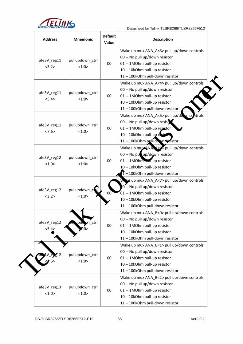
Datasheet for Telink TLSR8266/TLSR8266F512
DS-TLSR8266/TLSR8266F512-E19 65 Ver2.0.2
Address Mnemonic Default
Value Description
afe3V_reg11
<3:2>
pullupdown_ctrl
<1:0> 00
Wake up mux ANA_A<3> pull up/down controls
00 -- No pull up/down resistor
01 -- 1MOhm pull-up resistor
10 – 10kOhm pull-up resistor
11 – 100kOhm pull-down resistor
afe3V_reg11
<5:4>
pullupdown_ctrl
<1:0> 00
Wake up mux ANA_A<4> pull up/down controls
00 -- No pull up/down resistor
01 -- 1MOhm pull-up resistor
10 – 10kOhm pull-up resistor
11 – 100kOhm pull-down resistor
afe3V_reg11
<7:6>
pullupdown_ctrl
<1:0> 00
Wake up mux ANA_A<5> pull up/down controls
00 -- No pull up/down resistor
01 -- 1MOhm pull-up resistor
10 – 10kOhm pull-up resistor
11 – 100kOhm pull-down resistor
afe3V_reg12
<1:0>
pullupdown_ctrl
<1:0> 00
Wake up mux ANA_A<6> pull up/down controls
00 -- No pull up/down resistor
01 -- 1MOhm pull-up resistor
10 – 10kOhm pull-up resistor
11 – 100kOhm pull-down resistor
afe3V_reg12
<3:2>
pullupdown_ctrl
<1:0> 00
Wake up mux ANA_A<7> pull up/down controls
00 -- No pull up/down resistor
01 -- 1MOhm pull-up resistor
10 – 10kOhm pull-up resistor
11 – 100kOhm pull-down resistor
afe3V_reg12
<5:4>
pullupdown_ctrl
<1:0> 00
Wake up mux ANA_B<0> pull up/down controls
00 -- No pull up/down resistor
01 -- 1MOhm pull-up resistor
10 – 10kOhm pull-up resistor
11 – 100kOhm pull-down resistor
afe3V_reg12
<7:6>
pullupdown_ctrl
<1:0> 00
Wake up mux ANA_B<1> pull up/down controls
00 -- No pull up/down resistor
01 -- 1MOhm pull-up resistor
10 – 10kOhm pull-up resistor
11 – 100kOhm pull-down resistor
afe3V_reg13
<1:0>
pullupdown_ctrl
<1:0> 00
Wake up mux ANA_B<2> pull up/down controls
00 -- No pull up/down resistor
01 -- 1MOhm pull-up resistor
10 – 10kOhm pull-up resistor
11 – 100kOhm pull-down resistor
Telink for customer

Datasheet for Telink TLSR8266/TLSR8266F512
DS-TLSR8266/TLSR8266F512-E19 66 Ver2.0.2
Address Mnemonic Default
Value Description
afe3V_reg13
<3:2>
pullupdown_ctrl
<1:0> 00
Wake up mux ANA_B<3> pull up/down controls
00 -- No pull up/down resistor
01 -- 1MOhm pull-up resistor
10 – 10kOhm pull-up resistor
11 – 100kOhm pull-down resistor
afe3V_reg13
<5:4>
pullupdown_ctrl
<1:0> 00 rsvd
afe3V_reg13
<7:6>
pullupdown_ctrl
<1:0> 00
Wake up mux ANA_B<5> pull up/down controls
00 -- No pull up/down resistor
01 -- 1MOhm pull-up resistor
10 – 10kOhm pull-up resistor
11 – 100kOhm pull-down resistor
afe3V_reg14
<1:0>
pullupdown_ctrl
<1:0> 00
Wake up mux ANA_B<6> pull up/down controls
00 -- No pull up/down resistor
01 -- 1MOhm pull-up resistor
10 – 10kOhm pull-up resistor
11 – 100kOhm pull-down resistor
afe3V_reg14
<3:2>
pullupdown_ctrl
<1:0> 00
Wake up mux ANA_B<7> pull up/down controls
00 -- No pull up/down resistor
01 -- 1MOhm pull-up resistor
10 – 10kOhm pull-up resistor
11 – 100kOhm pull-down resistor
afe3V_reg14
<5:4>
pullupdown_ctrl
<1:0> 00
Wake up mux ANA_C<0> pull up/down controls
00 -- No pull up/down resistor
01 -- 1MOhm pull-up resistor
10 – 10kOhm pull-up resistor
11 – 100kOhm pull-down resistor
afe3V_reg14
<7:6>
pullupdown_ctrl
<1:0> 00
Wake up mux ANA_C<1> pull up/down controls
00 -- No pull up/down resistor
01 -- 1MOhm pull-up resistor
10 – 10kOhm pull-up resistor
11 – 100kOhm pull-down resistor
afe3V_reg15
<1:0>
pullupdown_ctrl
<1:0> 00
Wake up mux ANA_C<2> pull up/down controls
00 -- No pull up/down resistor
01 -- 1MOhm pull-up resistor
10 – 10kOhm pull-up resistor
11 – 100kOhm pull-down resistor
afe3V_reg15
<3:2>
pullupdown_ctrl
<1:0> 00
Wake up mux ANA_C<3> pull up/down controls
00 -- No pull up/down resistor
01 -- 1MOhm pull-up resistor
10 – 10kOhm pull-up resistor
Telink for customer
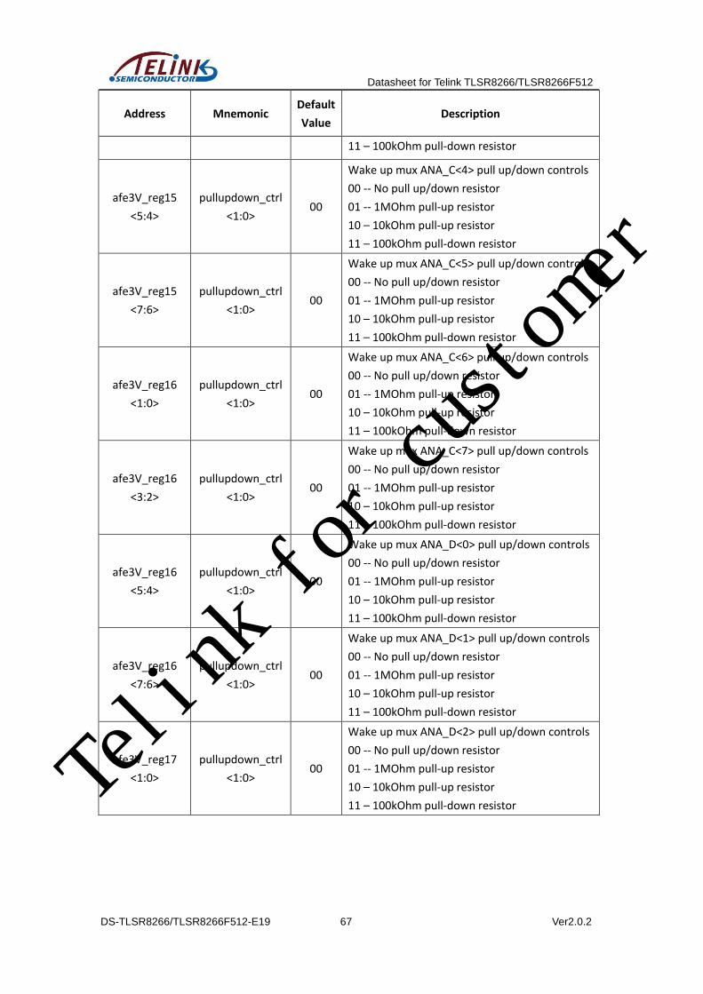
Datasheet for Telink TLSR8266/TLSR8266F512
DS-TLSR8266/TLSR8266F512-E19 67 Ver2.0.2
Address Mnemonic Default
Value Description
11 – 100kOhm pull-down resistor
afe3V_reg15
<5:4>
pullupdown_ctrl
<1:0> 00
Wake up mux ANA_C<4> pull up/down controls
00 -- No pull up/down resistor
01 -- 1MOhm pull-up resistor
10 – 10kOhm pull-up resistor
11 – 100kOhm pull-down resistor
afe3V_reg15
<7:6>
pullupdown_ctrl
<1:0> 00
Wake up mux ANA_C<5> pull up/down controls
00 -- No pull up/down resistor
01 -- 1MOhm pull-up resistor
10 – 10kOhm pull-up resistor
11 – 100kOhm pull-down resistor
afe3V_reg16
<1:0>
pullupdown_ctrl
<1:0> 00
Wake up mux ANA_C<6> pull up/down controls
00 -- No pull up/down resistor
01 -- 1MOhm pull-up resistor
10 – 10kOhm pull-up resistor
11 – 100kOhm pull-down resistor
afe3V_reg16
<3:2>
pullupdown_ctrl
<1:0> 00
Wake up mux ANA_C<7> pull up/down controls
00 -- No pull up/down resistor
01 -- 1MOhm pull-up resistor
10 – 10kOhm pull-up resistor
11 – 100kOhm pull-down resistor
afe3V_reg16
<5:4>
pullupdown_ctrl
<1:0> 00
Wake up mux ANA_D<0> pull up/down controls
00 -- No pull up/down resistor
01 -- 1MOhm pull-up resistor
10 – 10kOhm pull-up resistor
11 – 100kOhm pull-down resistor
afe3V_reg16
<7:6>
pullupdown_ctrl
<1:0> 00
Wake up mux ANA_D<1> pull up/down controls
00 -- No pull up/down resistor
01 -- 1MOhm pull-up resistor
10 – 10kOhm pull-up resistor
11 – 100kOhm pull-down resistor
afe3V_reg17
<1:0>
pullupdown_ctrl
<1:0> 00
Wake up mux ANA_D<2> pull up/down controls
00 -- No pull up/down resistor
01 -- 1MOhm pull-up resistor
10 – 10kOhm pull-up resistor
11 – 100kOhm pull-down resistor Telink for customer

Datasheet for Telink TLSR8266/TLSR8266F512
DS-TLSR8266/TLSR8266F512-E19 68 Ver2.0.2
Address Mnemonic Default
Value Description
afe3V_reg17
<3:2>
pullupdown_ctrl
<1:0> 00
Wake up mux ANA_D<3> pull up/down controls
00 -- No pull up/down resistor
01 -- 1MOhm pull-up resistor
10 – 10kOhm pull-up resistor
11 – 100kOhm pull-down resistor
afe3V_reg17
<5:4>
pullupdown_ctrl
<1:0> 00
Wake up mux ANA_D<4> pull up/down controls
00 -- No pull up/down resistor
01 -- 1MOhm pull-up resistor
10 – 10kOhm pull-up resistor
11 – 100kOhm pull-down resistor
afe3V_reg17
<7:6>
pullupdown_ctrl
<1:0> 00
Wake up mux ANA_D<5> pull up/down controls
00 -- No pull up/down resistor
01 -- 1MOhm pull-up resistor
10 – 10kOhm pull-up resistor
11 – 100kOhm pull-down resistor
afe3V_reg18
<1:0>
pullupdown_ctrl
<1:0> 00
Wake up mux ANA_D<6> pull up/down controls
00 -- No pull up/down resistor
01 -- 1MOhm pull-up resistor
10 – 10kOhm pull-up resistor
11 – 100kOhm pull-down resistor
afe3V_reg18
<3:2>
pullupdown_ctrl
<1:0> 00
Wake up mux ANA_D<7> pull up/down controls
00 -- No pull up/down resistor
01 -- 1MOhm pull-up resistor
10 – 10kOhm pull-up resistor
11 – 100kOhm pull-down resistor
afe3V_reg18
<5:4>
pullupdown_ctrl
<1:0> 00
Wake up mux ANA_E<0> pull up/down controls
00 -- No pull up/down resistor
01 -- 1MOhm pull-up resistor
10 – 10kOhm pull-up resistor
11 – 100kOhm pull-down resistor
afe3V_reg18
<7:6>
pullupdown_ctrl
<1:0> 00
Wake up mux ANA_E<1> pull up/down controls
00 -- No pull up/down resistor
01 -- 1MOhm pull-up resistor
10 – 10kOhm pull-up resistor
11 – 100kOhm pull-down resistor
afe3V_reg19
<1:0>
pullupdown_ctrl
<1:0> 00
Wake up mux ANA_E<2> pull up/down controls
00 -- No pull up/down resistor
01 -- 1MOhm pull-up resistor
10 – 10kOhm pull-up resistor
11 – 100kOhm pull-down resistor
Telink for customer

Datasheet for Telink TLSR8266/TLSR8266F512
DS-TLSR8266/TLSR8266F512-E19 69 Ver2.0.2
Address Mnemonic Default
Value Description
afe3V_reg19
<3:2>
pullupdown_ctrl
<1:0> 00
Wake up mux ANA_E<3> pull up/down controls
00 -- No pull up/down resistor
01 -- 1MOhm pull-up resistor
10 – 10kOhm pull-up resistor
11 – 100kOhm pull-down resistor
afe3V_reg19
<5:4>
pullupdown_ctrl
<1:0> 00
Wake up mux ANA_E<4> pull up/down controls
00 -- No pull up/down resistor
01 -- 1MOhm pull-up resistor
10 – 10kOhm pull-up resistor
11 – 100kOhm pull-down resistor
afe3V_reg19
<7:6>
pullupdown_ctrl
<1:0> 00
Wake up mux ANA_E<5> pull up/down controls
00 -- No pull up/down resistor
01 -- 1MOhm pull-up resistor
10 – 10kOhm pull-up resistor
11 – 100kOhm pull-down resistor
afe3V_reg20
<1:0>
pullupdown_ctrl
<1:0> 00
Wake up mux ANA_E<6> pull up/down controls
00 -- No pull up/down resistor
01 -- 1MOhm pull-up resistor
10 – 10kOhm pull-up resistor
11 – 100kOhm pull-down resistor
afe3V_reg20
<3:2>
pullupdown_ctrl
<1:0> 00
Wake up mux ANA_E<7> pull up/down controls
00 -- No pull up/down resistor
01 -- 1MOhm pull-up resistor
10 – 10kOhm pull-up resistor
11 – 100kOhm pull-down resistor
afe3V_reg20
<5:4>
pullupdown_ctrl
<1:0> 00
Wake up mux ANA_F<0> pull up/down controls
00 -- No pull up/down resistor
01 -- 1MOhm pull-up resistor
10 – 10kOhm pull-up resistor
11 – 100kOhm pull-down resistor
afe3V_reg20
<7:6>
pullupdown_ctrl
<1:0> 00
Wake up mux ANA_F<1> pull up/down controls
00 -- No pull up/down resistor
01 -- 1MOhm pull-up resistor
10 – 10kOhm pull-up resistor
11 – 100kOhm pull-down resistor
Telink for customer

Datasheet for Telink TLSR8266/TLSR8266F512
DS-TLSR8266/TLSR8266F512-E19 70 Ver2.0.2
7.2 SWM and SWS
The TLSR8266/TLSR8266F512 supports Single Wire interface. SWM (Single Wire
Master) and SWS (Single Wire Slave) represent the master and slave device of the
single wire communication system developed by Telink. The maximum data rate can
be up to 2Mbps.
7.3 I2C
The TLSR8266/TLSR8266F512 embeds I2C hardware module, which could act as
Master mode or Slave mode. I2C is a popular inter-IC interface requiring only 2 bus
lines, a serial data line (SDA) and a serial clock line (SCL).
7.3.1 Communication protocol
Telink I2C module supports standard mode (100kbps), Fast-mode (400kbps),
Fast-mode plus (1Mbps) and High-speed mode (3.4Mbps) with restriction that system
clock must be by at least 10x of data rate.
Two wires, SDA and SCL carry information between Master device and Slave
device connected to the bus. Each device is recognized by unique address (ID). Master
device is the device which initiates a data transfer on the bus and generates the clock
signals to permit that transfer. Slave device is the device addressed by a master.
Both SDA and SCL are bidirectional lines connected to a positive supply voltage
via a pull-up resister. When the bus is free, both lines are HIGH. It’s noted that data in
SDA line must keep stable when clock signal in SCL line is at high level, and level state
in SDA line is only allowed to change when clock signal in SCL line is at low level.
Figure 7- 2 I2C timing chart
Telink for customer
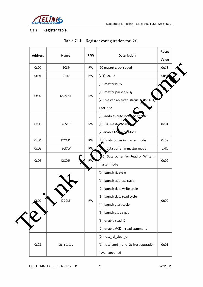
Datasheet for Telink TLSR8266/TLSR8266F512
DS-TLSR8266/TLSR8266F512-E19 71 Ver2.0.2
7.3.2 Register table
Table 7- 4 Register configuration for I2C
Address Name R/W Description Reset
Value
0x00 I2CSP RW I2C master clock speed 0x13
0x01 I2CID RW [7:1] I2C ID 0x5c
0x02 I2CMST RW
[0]: master busy
[1]: master packet busy
[2]: master received status: 0 for ACK;
1 for NAK
0x03 I2CSCT RW
[0]: address auto increase enable
[1]: I2C master enable
[2] enable Mapping Mode
0x01
0x04 I2CAD RW [7:0] data buffer in master mode 0x5a
0x05 I2CDW RW [7:0] Data buffer in master mode 0xf1
0x06 I2CDR RW [7:0] Data buffer for Read or Write in
master mode 0x00
0x07 I2CCLT RW
[0]: launch ID cycle
[1]: launch address cycle
[2]: launch data write cycle
[3]: launch data read cycle
[4]: launch start cycle
[5]: launch stop cycle
[6]: enable read ID
[7]: enable ACK in read command
0x00
0x21 i2c_status
[0]:host_rd_clear_en
[1]:host_cmd_irq_o:i2c host operation
have happened
0x01
Telink for customer

Datasheet for Telink TLSR8266/TLSR8266F512
DS-TLSR8266/TLSR8266F512-E19 72 Ver2.0.2
Address Name R/W Description Reset
Value
[2]:host_rd_tag_stat:i2c host
operation have happened and is read
operation
0x22 clear_stats
[0]:write 1 clear software_irq
[1]:write 1 clear host_cmd_irq
[2]:write 1 clear host_rd_tag_stat
[4]:write 1 set software_irq
[5]write 1 clear ana_irq
0x3e Reg_host_map_adrl R/W Lower byte of Mapping mode buffer
address 0x80
0x3f Reg_host_map_adrh R/W Higher byte of Mapping mode buffer
address 0xd7
0x20 Reg_host_map_status R [6:0] I2C read address 0x00
7.3.3 I2C Slave mode
I2C module of the TLSR8266/TLSR8266F512 acts as Slave mode by default. I2C
slave address can be configured via register I2CID (address 0x01) [7:1].
Figure 7- 3 Byte consisted of slave address and R/W flag bit
I2C slave mode supports two sub modes including Direct Memory Access (DMA)
mode and Mapping mode, which is selectable via address 0x03[2].
In I2C Slave mode, Master could initiate transaction anytime. I2C slave module
will reply with ACK automatically. To monitor the start of I2C transaction, user could
set interrupt from GPIO for SCA or SCL.
Telink for customer

Datasheet for Telink TLSR8266/TLSR8266F512
DS-TLSR8266/TLSR8266F512-E19 73 Ver2.0.2
7.3.3.1 DMA mode
In DMA mode, other devices (Master) could access (read/write) designated
address in Register and/or SRAM of the TLSR8266/TLSR8266F512 according to I2C
protocol. I2C module of the TLSR8266/TLSR8266F512 will execute the read/write
command from I2C master automatically. But user needs to notice that the system
clock shall be at least 10x faster than I2C bit rate.
The access address designated by Master is offset by 0x800000. In the
TLSR8266/TLSR8266F512, Register address starts from 0x800000 and SRAM address
starts from 0x808000. For example, if Addr High(AddrH) is 0xaa and Addr Low (AddrL)
is 0xcc, the real address of accessed data is 0x80aacc.
In DMA mode, Master could read/write data byte by byte. The designated access
address is initial address and it supports auto increment by setting address 0x03[0] to
1b’1.
START ID W
8 bits
ACK AddrH ACK AddrL ACK
DATA ACK
STOP
8 bits 8 bits
8 bits
Read Format in DMA mode
START ID R
8 bits
ACK NAK STOP
Figure 7- 4 Read format in DMA mode
START ID W
8 bits
ACK AddrH ACK AddrL ACK DATA ACK STOP
8 bits 8 bits 8 bits
Write Format in DMA mode
Figure 7- 5 Write format in DMA mode
Telink for customer

Datasheet for Telink TLSR8266/TLSR8266F512
DS-TLSR8266/TLSR8266F512-E19 74 Ver2.0.2
7.3.3.2 Mapping mode
Mapping mode could be enabled via setting register I2CSCT (address 0x03)[2] to
1b’1.
In Mapping mode, data written and read by I2C master will be redirected to
specified 128-byte buffer in SRAM. User could specify the initial address of the buffer
by configuring registers reg_host_map_adrl (address 0x3e, lower byte) and
reg_host_map_adrh (address 0x3f, higher byte). The first 64-byte buffer is for written
data and following 64-byte buffer is for read data. Every time the data access will start
from the beginning of the Write-buffer/Read-buffer after I2C stop condition occurs.
The last accessed data address could be checked in register reg_host_map_status
(address 0x20) [6:0] which is only updated after I2C STOP occurs.
DATA ACK
8 bits
Read Format in mapping mode
START ID R
8 bits
ACK NAK STOP
Figure 7- 6 Read format in Mapping mode
START ID W
8 bits
ACK DATA ACK STOP
8 bits
Write Format in mapping mode
Figure 7- 7 Write format in Mapping mode
7.3.4 I2C Master mode
Address 0x03[1] should be set to 1b’1 to enable I2C master mode for the
TLSR8266/TLSR8266F512.
Address 0x00 serves to set I2C Master clock: FI2C = System Clock / (2 *clock speed
configured in address 0x00).
A complete I2C protocol contains START, Slave Address, R/W bit, data, ACK and
STOP. Slave address could be configured via address 0x01[7:1].
Telink for customer

Datasheet for Telink TLSR8266/TLSR8266F512
DS-TLSR8266/TLSR8266F512-E19 75 Ver2.0.2
I2C Master could send START, Slave Address, R/W bit, data and STOP by
configuring address 0x07. I2C master will send enabled cycles with correct sequence.
Address 0x02 serves to indicate whether Master/Master packet is busy, as well as
Master received status. Bit[0] will be set to 1 when one byte is being sent, and the bit
can be automatically cleared after a start signal/ address byte/acknowledge
signal/data /stop signal is sent. Bit[1] is set to 1 when the start signal is sent, and the
bit will be automatically cleared after the stop signal is sent. Bit[2] indicates whether
to succeed in sending acknowledgement signal.
7.3.4.1 I2C Master Write transfer
I2C Master has 3 byte buffer for write data, which are I2CAD (0x04), I2CDW (0x05)
and I2CDR (0x06). Write transfer will be completed by I2C master module.
For example, to implement an I2C write transfer with 3 byte data, which contains
START, Slave Address, Write bit, ack from Slave, 1st byte, ack from slave, 2nd byte, ack
from slave, 3rd byte, ack from slave and STOP, user needs to configure I2C slave
address to I2CID (0x01) [7:1], 1st byte data to I2CAD, 2nd byte data to I2CDW and 3rd
byte to I2CDR. To start I2C write transfer, I2CCLT (0x07) is configured to 0x3f. I2C
Master will launch START, Slave address, Write bit, load ACK to I2CMST (0x02) [2],
send I2CAD data, load ACK to I2CMST[2], send I2CDW data, load ACK to I2CMST[2],
send I2CDR data, load ACK to I2CMST[2] and then STOP sequentially.
For I2C write transfer whose data is more than 3 bytes, user could split the cycles
according to I2C protocol.
7.3.4.2 I2C Master Read transfer
I2C Master has one byte buffer for read data, which is I2CDR (0x06). Read
transfer will be completed by I2C Master.
For example, to implement an I2C read transfer with 1 byte data, which contains
START, Slave Address, Read bit, Ack from Slave, 1st byte from Slave, Ack by master and
STOP, user needs to configure I2C slave address to I2CID (0x01) [7:1]. To start I2C read
transfer, I2CCLT (0x07) is configured to 0xf9. I2C Master will launch START, Slave
Telink for customer

Datasheet for Telink TLSR8266/TLSR8266F512
DS-TLSR8266/TLSR8266F512-E19 76 Ver2.0.2
address, Read bit, load ACK to I2CMST (0x02) [2], load data to I2CDR, reply ACK and
then STOP sequentially.
For I2C read transfer whose data is more than 1 bytes, user could split the cycles
according to I2C protocol.
7.4 SPI
The TLSR8266/TLSR8266F512 embeds SPI (Serial Peripheral interface), which
could act as Master mode or Slave mode. SPI is a high-speed, full-duplex and
synchronous communication bus requiring 4 bus lines including a chip select (CS) line,
a data input (DI) line, a data output (DO) line and a clock (CK) line.
7.4.1 Register table
Table 7- 5 Register configuration for SPI
Address Name R/W Description Reset
Value
0x08 SPIDAT RW SPI data access
0x09 SPICT RW
[0]: p_csn
[1]: enable master mode
[2]: spi data output disable
[3]: 1 for read command; 0 for write
command
[4]: address auto increase
[5]: share_mode
[6]: busy status
11
0x0a SPISP RW
[6:0]: SPI clock speed
[7]: SPI function mode, p_csn, p_scl,
p_sda and p_sdo function as SPI if 1
05
0x0b SPIMODE RW [0]: inverse SPI clock output
[1]: dat delay half clk 0
Telink for customer

Datasheet for Telink TLSR8266/TLSR8266F512
DS-TLSR8266/TLSR8266F512-E19 77 Ver2.0.2
Address Name R/W Description Reset
Value
0x0c MSPIDAT RW Memory SPI data access
0x0d MSPICT RW
[0]: p_mcsn
[1]: rsvd
[2]: continuous mode
[3]: 1 for read command; 0 for write
command
[4]: address auto increase
11
0x0e MSPIRA RW Memory SPI read command ID 0b
0x0f MSPIMODE RW [0]: dual data mode
[1]: dual address mode
[7:2]: MSPI clock speed
0
7.4.2 SPI Master mode
SPI for the TLSR8266/TLSR8266F512 supports both master mode and slave mode
and acts as slave mode by default. Address 0x09 bit[1] should be set to 1b’1 to enable
SPI Master mode.
Register SPISP is to configure SPI pin and clock: setting address 0x0a bit[7] to 1 is
to enable SPI function mode, and corresponding pins can be used as SPI pins; SPI clock
= system clock/((clock speed configured in address 0x0a bit[6:0] +1)*2).Address 0x08
serves as the data register. One reading/writing operation of 0x08 enables the SPI_CK
pin to generate 8 SPI clock cycles.
Telink SPI supports four standard working modes: Mode 0~Mode 3. Register
SPIMODE (address 0x0b) serves to select one of the four SPI modes:
Telink for customer

Datasheet for Telink TLSR8266/TLSR8266F512
DS-TLSR8266/TLSR8266F512-E19 78 Ver2.0.2
Table 7- 6 SPI mode
SPI mode CPOL/CPHA SPIMODE register
(Address 0x0b)
Mode 0 CPOL=0, CPHA=0 bit[0]=0, bit[1]=0
Mode 1 CPOL=0, CPHA=1 bit[0]=0, bit[1]=1
Mode 2 CPOL=1, CPHA=0 bit[0]=1, bit[1]=0
Mode 3 CPOL=1, CPHA=1 bit[0]=1, bit[1]=1
CPOL: Clock Polarity
When CPOL=0, SPI_CLK keeps low level in idle state;
When CPOL=1, SPI_CLK keeps high level in idle state.
CPHA: Clock Phase
When CPHA=0, data is sampled at the first edge of clock period
When CPHA=1, data is sampled at the latter edge of clock period
Address 0x09 bit[0] is to control the CS line: when the bit is set to 1, the CS level
is high; when the bit is cleared, the CS level is low. Address 0x09 bit[2] is the disabling
bit for SPI Master output. When the bit is cleared, MCU writes data into address 0x08,
then the SPI_DO pin outputs the data bit by bit during the 8 clock cycles generated by
the SPI_CK pin. When the bit is set to 1b’1, SPI_DO output is disabled.
Address 0x09 bit[3] is the enabling bit for SPI Master reading data function.
When the bit is set to 1b’1, MCU reads the data from address 0x08, then the input
data from the SPI_DI pin is shifted into address 0x08 during the 8 clock cycles
generated by the SPI_CK pin. When the bit is cleared, SPI Master reading function is
disabled.Address 0x09[5] is the enabling bit for share mode, i.e. whether SPI_DI and
SPI_DO share one common line.
Users can read address 0x09 bit[6] to get SPI busy status, i.e. whether the 8 clock
pulses have been sent.
7.4.3 SPI Slave mode
SPI for the TLSR8266/TLSR8266F512 acts as slave mode by default. SPI Slave
mode support DMA. User could access registers of the TLSR8266/TLSR8266F512 by
SPI interface. It’s noted that system clock of TLSR8266/TLSR8266F512 shall be at least
5x faster than SPI clock for reliable connection. Address 0x0a should be written with
data 0xa5 by the SPI host to activate SPI slave mode.
Telink for customer
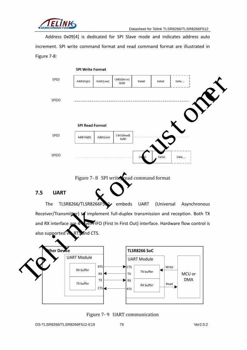
Datasheet for Telink TLSR8266/TLSR8266F512
DS-TLSR8266/TLSR8266F512-E19 79 Ver2.0.2
Address 0x09[4] is dedicated for SPI Slave mode and indicates address auto
increment. SPI write command format and read command format are illustrated in
Figure 7-8:
Figure 7- 8 SPI write/read command format
7.5 UART
The TLSR8266/TLSR8266F512 embeds UART (Universal Asynchronous
Receiver/Transmitter) to implement full-duplex transmission and reception. Both TX
and RX interface are 4-layer FIFO (First In First Out) interface. Hardware flow control is
also supported via RTS and CTS.
RTS
TX
RX
CTS
MCU or DMA
Write
Read
TLSR8266 SoC
RX
RTS
TX
CTS
Other Device
RX buffer
TX buffer
UART Module
TX buffer
RX buffer
UART Module
Figure 7- 9 UART communication
Telink for customer

Datasheet for Telink TLSR8266/TLSR8266F512
DS-TLSR8266/TLSR8266F512-E19 80 Ver2.0.2
As shown in Figure 7-9, data to be sent is first written into TX buffer by MCU or
DMA, then UART module transmits the data from TX buffer to other device via pin TX.
Data to be read from other device is first received via pin RX and sent to RX buffer,
then the data is read by MCU or DMA.
If RX buffer of the TLSR8266/TLSR8266F512 UART is close to full, the
TLSR8266/TLSR8266F512 will send a signal (configurable high or low level) via pin RTS
to inform other device that it should stop sending data. Similarly, if the
TLSR8266/TLSR8266F512 receives a signal from pin CTS, it indicates that RX buffer of
other device is close to full and the TLSR8266/TLSR8266F512 should stop sending
data.
Table 7- 7 Register configuration for UART
Address Name R/W Description Reset
Value
0x90 uart_data_buf0 R/W write/read buffer[7:0]
0x91 Uart_data_buf1 R/W Write/read buffer[15:8]
0x92 Uart_data_buf2 RW Write/read buffer[23:16]
0x93 Uart_data_buf3 R/W Write/read buffer[31:24]
0x94 uart_clk_div[7:0] RW uart clk div register: 0xff
0x95 Uart_clk_div[15:8] R/W uart_sclk = sclk/(uart_clk_div[14:0]+1) uart_clk_div[15] : 1:enable clock divider,0: disable.
0x0f
0x96 Uart ctrl0 R/W
[3:0] bwpc, bit width, should be larger than 2 Baudrate = uart_sclk/(bwpc+1) [4] rx dma enable [5] tx dma enable [6] rx interrupt enable [7]tx interrupt enable
0x0f
0x97 Uart_ctrl1 R/W
[0] cts select, 0: cts_i, 1: cts _i inverter [1]:cts enable, 1: enable, 0, disable [2]:Parity, 1: enable, 0 :disable [3]: even Parity or odd [5:4]: stop bit 00: 1 bit, 01, 1.5bit 1x: 2bits [6]: ttl [7] uart tx, rx loopback
0x0e
0x98 Uart_ctrl2 R/W
[3:0] rts trig level [4] rts Parity [5] rts manual value [6] rts manual enable [7] rts enable
0xa5
Telink for customer

Datasheet for Telink TLSR8266/TLSR8266F512
DS-TLSR8266/TLSR8266F512-E19 81 Ver2.0.2
Address Name R/W Description Reset
Value
0x99 Uart_ctrl3 R/W [3:0]: rx_irq_trig level [7:4] tx_irq_trig level
0x44
0x9a R_rxtimeout_o[7:0] R/W
The setting is transfer one bytes need cycles base on uart_clk. For example, if transfer one bytes (1start bit+8bits data+1 priority bit+2stop bits) total 12 bits, this register setting should be (bwpc+1)*12.
0x0f
0x9b R_rxtimeout_o[9:8] R/W
2’b00:rx timeout time is r_rxtimeout[7:0] 2’b01:rx timeout time is r_rxtimeout[7:0]*2 2’b10:rx timeout time is r_rxtimeout[7:0]*3 3’b11: rx timeout time is r_rxtimeout[7:0]*4 R_rxtimeout is for rx dma to decide the end of each transaction. Supposed the interval between each byte in one transaction is very short.
0x00
0x9c Buf_cnt R [3:0]: r_buf_cnt [7:4]:t_buf_cnt
0x9d Uart_sts R
[2:0] rbcnt [3] irq [6:4]wbcnt [6] write 1 clear rx [7] rx_err, write 1 clear tx
Addresses 0x90~0x93 serve to write data into TX buffer or read data from RX
buffer.
Addresses 0x94~0x95 serve to configure UART clock.
Address 0x96 serves to set baud rate (bit[3:0]), enable RX/TX DMA mode
(bit[4:5]), and enable RX/TX interrupt (bit[6:7]).
Address 0x97 mainly serves to configure CTS. Bit[1] should be set to 1b’1 to
enable CTS. Bit[0] serves to configure CTS signal level. Bit[2:3] serve to enable parity
bit and select even/odd parity. Bit[5:4] serve to select 1/1.5/2 bits for stop bit. Bit[6]
serves to configure whether RX/TX level should be inverted.
Address 0x98 serves to configure RTS. Bit[7] and Bit[3:0] serve to enable RTS and
configure RTS signal level.
Telink for customer
Datasheet for Telink TLSR8266/TLSR8266F512
DS-TLSR8266/TLSR8266F512-E19 82 Ver2.0.2
Address 0x99 serves to configure the number of bytes in RX/TX buffer to trigger
interrupt.
The number of bytes in RX/TX buffer can be read from address 0x9c.
Telink for customer

Datasheet for Telink TLSR8266/TLSR8266F512
DS-TLSR8266/TLSR8266F512-E19 83 Ver2.0.2
8 PWM
The TLSR8266/TLSR8266F512 supports 6-channel PWM
(Pulse-Width-Modulation) output. Each PWM#n has its corresponding inverted output
at PWM#n_Npin.
8.1 Register table
Table 8- 1 Register table for PWM
Address Mnemonic Type Description Reset
Value
0x780 PWM_EN R/W
[0]: 0--disable PWM0, 1--enable PWM0
[1]: 0--disable PWM1, 1--enable PWM1
[2]: 0--disable PWM2, 1--enable PWM2
[3]: 0--disable PWM3, 1--enable PWM3
[4]: 0--disable PWM4, 1--enable PWM4
[5]: 0--disable PWM5, 1--enable PWM5
0x00
0x781 PWM_CLK R/W (PWM_CLK+1)*sys_clk 0x00
0x782 PWM_MODE R/W
[1:0]: 00-pwm0 normal mode
[1:0]: 01-pwm0 count mode
[1:0]: 11-pwm0 IR mode
[3:2]: 00-pwm1 normal mode
[3:2]: 01-pwm1 count mode
[3:2]: 11-pwm1 IR mode
0x00
0x783 PWM_CC0 R/W [5:0]:1 ‘b1 invert PWM output 0x00
0x784 PWM_CC1 R/W [5:0]:1‘b1 invert PWM_INV output 0x00
0x785 PWM_CC2 R/W [5:0]:1’b1 PWM’ pola,low level first 0x00
0x788 PWM_PHASE0 R/W [7:0] bits 7-0 of PWM0's phase time 0x00
0x789 PWM_PHASE0 R/W [15:8] bits 15-8 of PWM0's phase time 0x00
0x78a PWM_PHASE1 R/W [7:0] bits 7-0 of PWM1's phase time 0x00
0x78b PWM_PHASE1 R/W [7:8] bits 15-8 of PWM1's phase time 0x00
0x78c PWM_PHASE2 R/W [7:0] bits 7-0 of PWM2's phase time 0x00
0x78d PWM_PHASE2 R/W [15:8] bits 15-8 of PWM2's phase time 0x00
0x78e PWM_PHASE3 R/W [7:0] bits 7-0 of PWM3's phase time 0x00
0x78f PWM_PHASE3 R/W [15:8] bits 15-8 of PWM3's phase time 0x00
0x790 PWM_PHASE4 R/W [7:0] bits 7-0 of PWM4's phase time 0x00
0x791 PWM_PHASE4 R/W [15:8] bits 15-8 of PWM4's phase time 0x00
0x792 PWM_PHASE5 R/W [7:0] bits 7-0 of PWM5's phase time 0x00
0x793 PWM_PHASE5 R/W [15:8] bits 15-8 of PWM5's phase time 0x00
Telink for customer

Datasheet for Telink TLSR8266/TLSR8266F512
DS-TLSR8266/TLSR8266F512-E19 84 Ver2.0.2
Address Mnemonic Type Description Reset
Value
0x794 PWM_TCMP0 R/W [7:0] bits 7-0 of PWM0's high time or low
time(if pola[0]=1) 0x00
0x795 PWM_TCMP0 R/W [15:8] bits 15-8 of PWM0's high time or
low time 0x00
0x796 PWM_TMAX0 R/W [7:0] bits 7-0 of PWM0's cycle time 0x00
0x797 PWM_TMAX0 R/W [15:8] bits 15-8 of PWM0's cycle time 0x00
0x798 PWM_TCMP1 R/W [7:0] bits 7-0 of PWM1's high time or low
time(if pola[1]=1) 0x00
0x799 PWM_TCMP1 R/W [15:8] bits 15-8 of PWM1's high time or
low time 0x00
0x79a PWM_TMAX1 R/W [7:0] bits 7-0 of PWM1's cycle time 0x00
0x79b PWM_TMAX1 R/W [15:8] bits 15-8 of PWM1's cycle time 0x00
0x79c PWM_TCMP2 R/W [7:0] bits 7-0 of PWM2's high time or low
time(if pola[2]=1) 0x00
0x79d PWM_TCMP2 R/W [15:8] bits 15-8 of PWM2's high time or
low time 0x00
0x79e PWM_TMAX2 R/W [7:0] bits 7-0 of PWM2's cycle time 0x00
0x79f PWM_TMAX2 R/W [15:8] bits 15-8 of PWM2's cycle time 0x00
0x7a0 PWM_TCMP3 R/W [7:0] bits 7-0 of PWM3's high time or low
time(if pola[3]=1) 0x00
0x7a1 PWM_TCMP3 R/W [15:8] bits 15-8 of PWM3's high time or
low time 0x00
0x7a2 PWM_TMAX3 R/W [7:0] bits 7-0 of PWM3's cycle time 0x00
0x7a3 PWM_TMAX3 R/W [15:8] bits 15-8 of PWM3's cycle time 0x00
0x7a4 PWM_TCMP4 R/W [7:0] bits 7-0 of PWM4's high time or low
time(if pola[4]=1) 0x00
0x7a5 PWM_TCMP4 R/W [15:8] bits 15-8 of PWM4's high time or
low time 0x00
0x7a6 PWM_TMAX4 R/W [7:0] bits 7-0 of PWM4's cycle time 0x00
0x7a7 PWM_TMAX4 [15:8] bits 15-8 of PWM4's cycle time 0x00
0x7a8 PWM_TCMP5 R/W [7:0] bits 7-0 of PWM5's high time or low
time(if pola[5]=1) 0x00
0x7a9 PWM_TCMP5 R/W [15:8] bits 15-8 of PWM5's high time or
low time 0x00
0x7aa PWM_TMAX5 R/W [7:0] bits 7-0 of PWM5's cycle time 0x00
0x7ab PWM_TMAX5 R/W [15:8] bits 15-8 of PWM5's cycle time 0x00
Telink for customer
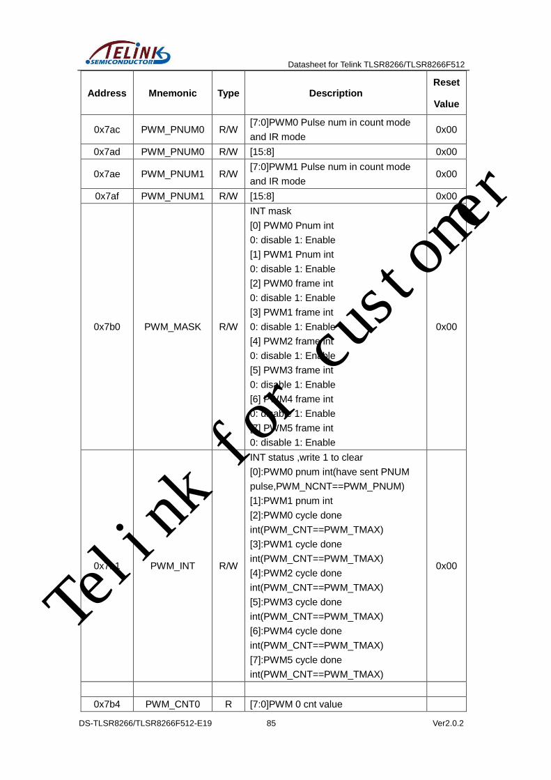
Datasheet for Telink TLSR8266/TLSR8266F512
DS-TLSR8266/TLSR8266F512-E19 85 Ver2.0.2
Address Mnemonic Type Description Reset
Value
0x7ac PWM_PNUM0 R/W [7:0]PWM0 Pulse num in count mode
and IR mode 0x00
0x7ad PWM_PNUM0 R/W [15:8] 0x00
0x7ae PWM_PNUM1 R/W [7:0]PWM1 Pulse num in count mode
and IR mode 0x00
0x7af PWM_PNUM1 R/W [15:8] 0x00
0x7b0 PWM_MASK R/W
INT mask
[0] PWM0 Pnum int
0: disable 1: Enable
[1] PWM1 Pnum int
0: disable 1: Enable
[2] PWM0 frame int
0: disable 1: Enable
[3] PWM1 frame int
0: disable 1: Enable
[4] PWM2 frame int
0: disable 1: Enable
[5] PWM3 frame int
0: disable 1: Enable
[6] PWM4 frame int
0: disable 1: Enable
[7] PWM5 frame int
0: disable 1: Enable
0x00
0x7b1 PWM_INT R/W
INT status ,write 1 to clear
[0]:PWM0 pnum int(have sent PNUM
pulse,PWM_NCNT==PWM_PNUM)
[1]:PWM1 pnum int
[2]:PWM0 cycle done
int(PWM_CNT==PWM_TMAX)
[3]:PWM1 cycle done
int(PWM_CNT==PWM_TMAX)
[4]:PWM2 cycle done
int(PWM_CNT==PWM_TMAX)
[5]:PWM3 cycle done
int(PWM_CNT==PWM_TMAX)
[6]:PWM4 cycle done
int(PWM_CNT==PWM_TMAX)
[7]:PWM5 cycle done
int(PWM_CNT==PWM_TMAX)
0x00
0x7b4 PWM_CNT0 R [7:0]PWM 0 cnt value
Telink for customer

Datasheet for Telink TLSR8266/TLSR8266F512
DS-TLSR8266/TLSR8266F512-E19 86 Ver2.0.2
Address Mnemonic Type Description Reset
Value
0x7b5 PWM_CNT0 [15:8]PWM 0 cnt value
0x7b6 PWM_CNT1 R [7:0]PWM 1 cnt value
0x7b7 PWM_CNT1 [15:8]PWM 1 cnt value
0x7b8 PWM_CNT2 R [7:0]PWM 2 cnt value
0x7b9 PWM_CNT2 [15:8]PWM 2 cnt value
0x7ba PWM_CNT3 R [7:0]PWM 3 cnt value
0x7bb PWM_CNT3 [15:8]PWM 3 cnt value
0x7bc PWM_CNT4 R [7:0]PWM 4 cnt value
0x7bd PWM_CNT4 [15:8]PWM 4 cnt value
0x7be PWM_CNT5 R [7:0]PWM 5 cnt value
0x7bf PWM_CNT5 [15:8]PWM 5 cnt value
0x7c0 PWM_NCNT0 R [7:0]PWM0 pluse_cnt value
0x7c1 PWM_NCNT0 [15:8]PWM0 pluse_cnt value
0x7c2 PWM_NCNT1 R [7:0]PWM1 pluse_cnt value
0x7c3 PWM_NCNT1 [15:8]PWM1 pluse_cnt value
8.2 Enable PWM
Register PWM_EN (address 0x780)[5:0] serves to enable PWM5~PWM0
respectively via writing “1” for the corresponding bits.
8.3 Set PWM clock
PWM clock derives from system clock. Register PWM_CLK (address 0x781) serves
to set the frequency dividing factor for PWM clock. Formula below applies:
FPWM= FSystem clock / (PWM_CLK+1)
8.4 PWM waveform, polarity and output inversion
Each PWM channel has independent counter and 3 status including “Delay”,
“Count” and “Remaining”. Count and Remaining status form a signal frame.
8.4.1 PWM waveform
When PWM#n is enabled, PWM#n enters Delay status. By default PWM#n
outputs Low level at Delay status. The Delay status duration, i.e. Phase time, is
configured in register PWM_PHASE#n (address 0x788~0x793). Phase difference
Telink for customer

Datasheet for Telink TLSR8266/TLSR8266F512
DS-TLSR8266/TLSR8266F512-E19 87 Ver2.0.2
between PWM channels is allowed by different phase time configuration.
After Phase time expires, PWM#n exits Delay status and starts to send signal
frames. First PWM#n is at Count status and outputs High level signal by default. When
PWM#n counter reaches cycles set in register PWM_TCMP#n (address 0x794~0x795,
0x798~0x799, 0x79c~0x79d, 0x7a0~0x7a1, 0x7a4~0x7a5, 0x7a8~0x7a9), PWM#n
enters Remaining status and outputs Low level till PWM#n cycle time configured in
register PWM_TMAX#n (address 0x796~0x797, 0x79a~0x79b, 0x79e~0x79f,
0x7a2~0x7a3, 0x7a6~0x7a7, 0x7aa~0x7ab) expires.
An interruption will be generated at the end of each signal frame if enabled via
register PWM_MASK (address 0x7b0[2:7]).
8.4.2 Invert PWM output
PWM#n and PWM#n_N output could be inverted independently via register
PWM_CC0 (address 0x783) and PWM_CC1 (address 0x784). When the inversion bit is
enabled, the corresponding PWM channel waveform will be inverted completely.
8.4.3 Polarity for signal frame
By default, PWM#n outputs High level at Count status and Low level at
Remaining status. When the corresponding polarity bit is enabled via register
PWM_CC2 (address 0x785), PWM#n will output Low level at Count status and High
level at Remaining status.
Figure 8- 1 PWM output waveform chart
Telink for customer

Datasheet for Telink TLSR8266/TLSR8266F512
DS-TLSR8266/TLSR8266F512-E19 88 Ver2.0.2
8.5 PWM mode
8.5.1 Select PWM mode
PWM0 and PWM1 support 3 modes, including Continuous (normal) mode,
Counting mode, and IR mode. PWM2~PWM5 only support Continuous mode.
Register PWM_MODE (address 0x782) serves to select PWM0/PWM1 mode.
8.5.2 Continuous mode
PWM0~PWM5 all support Continuous mode. In this mode, PWM#n continuously
sends out signal frames. PWM#n should be disabled via address 0x780 to stop it;
when stopped, the PWM output will turn low immediately.
During Continuous mode, waveform could be changed freely. New configuration
for PWM_TCMP#n and PWM_TMAX#n will take effect in the next signal frame.
A frame interruption will be generated (if enabled) after each signal frame is finished.
Figure 8-2 Continuous mode
8.5.3 Counting mode
Only PWM0 and PWM1 support Counting mode. In this mode, PWM#n (n=0,1)
sends out specified number of signal frames which is defined as a pulse group. The
number is configured via register PWM_PNUM0 (address 0x7ac~0x7ad) and
PWM_PNUM1 (address 0x7ae~0x7af). After a pulse group is finished, PWM#n will be
disabled automatically, and a Pnum interruption will be generated if enabled via
register PWM_MASK (address 0x7b0[0:1]). Telink for customer

Datasheet for Telink TLSR8266/TLSR8266F512
DS-TLSR8266/TLSR8266F512-E19 89 Ver2.0.2
Figure 8-3 Counting mode
Counting mode also serves to stop IR mode gracefully. Refer to section 8.5.4 for
details.
8.5.4 IR mode
Only PWM0 and PWM1 support IR mode. In this mode, specified number of
frames is defined as one pulse group. In contrast to Counting mode where PWM#n
(n=0,1) stops after first pulse group finishes, PWM#n will constantly send pulse groups
in IR mode.
During IR mode, waveform could also be changed freely. New configuration for
PWM_TCMP#n and PWM_TMAX#n will take effect in the next pulse group.
To stop IR mode and complete current pulse group, user can switch PWM#n from
IR mode to Counting mode so that PWM#n will stop after current pulse group is
finished. If PWM#n is disabled directly via PWM_EN (0x780[0:1]), PWM#n output will
turn Low immediately despite of current pulse group.
A frame interruption/Pnum interruption will be generated (if enabled) after each
signal frame/pulse group is finished.
Telink for customer

Datasheet for Telink TLSR8266/TLSR8266F512
DS-TLSR8266/TLSR8266F512-E19 90 Ver2.0.2
Figure 8-4 IR mode
8.6 PWM interrupt
There are 8 interrupt sources from PWM function. After each signal frame,
PWM#n will generate a frame-done IRQ (Interrupt Request) signal. In Counting mode
and IR mode, PWM0/PWM1 will generate a Pnum IRQ signal after completing a pulse
group. Interrupt status can be cleared via register PWM_INT (address 0x7b1).
Telink for customer

Datasheet for Telink TLSR8266/TLSR8266F512
DS-TLSR8266/TLSR8266F512-E19 91 Ver2.0.2
9 Keyscan
The TLSR8266/TLSR8266F512 supports hardware Keyscan for power saving and
relieves MCU power to handle other tasks instead of keeping scanning IO.
9.1 Register table
Table 9- 1 Register table for Keyscan
Address Mnemonic Type Description Reset
Value
0x800 KS_COL_MSK0 RW Keyscan column mask for pe[7:0]
[7]: DI/I2C_SDA/ANA_E<7> (pe7)
[6]: CN/uart_rts/ANA_E<6> (pe6)
[5]: GP17/ANA_E<5> (pe5)
[4]: GP16/ANA_E<4> (pe4)
[3]: GP15/ANA_E<3> (pe3)
[2]: DMIC_DI/ANA_E<2> (pe2)
[1]: DMIC_CK/ANA_E<1> (pe1)
[0]: GP14/ANA_E<0> (pe0)
00
0x801 KS_COL_MSK1 RW Keyscan column mask for pd[7:0]
[7]: GP13/ANA_D<7> (pd7)
[6]: GP12/ANA_D<6>/Rbias_EXT (pd6)
[5]: GP11/ANA_D<5> (pd5)
[4]: GP10/ANA_D<4> (pd4)
[3]: GP9/PWM4/ANA_D<3> (pd3)
[2]: GP8/PWM3/ANA_D<2> (pd2)
[1]: GP7/uart_cts/ANA_D<1> (pd1)
[0]: GP6/uart_rts/ANA_D<0> (pd0)
00
0x802 KS_COL_MSK2 RW Keyscan column mask for pc[7:0]
[7]: GP5/uart_rx/ANA_C<7> (pc7)
00
Telink for customer
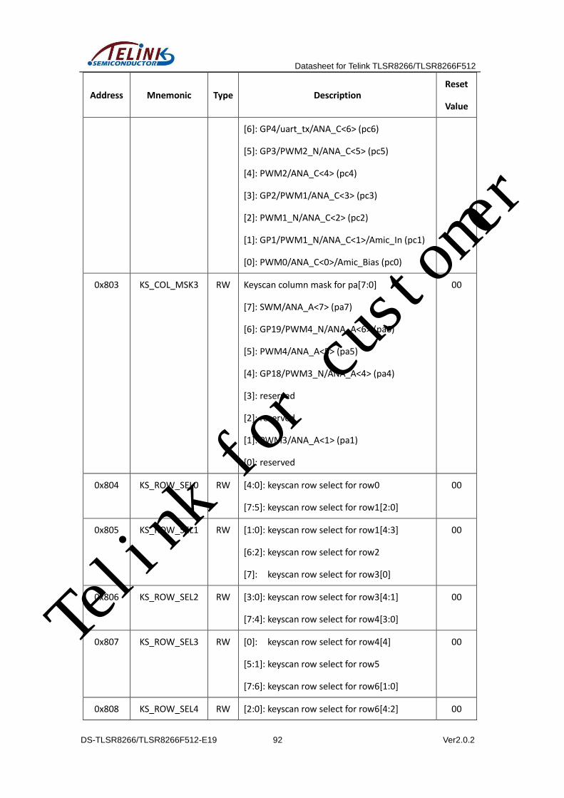
Datasheet for Telink TLSR8266/TLSR8266F512
DS-TLSR8266/TLSR8266F512-E19 92 Ver2.0.2
Address Mnemonic Type Description Reset
Value
[6]: GP4/uart_tx/ANA_C<6> (pc6)
[5]: GP3/PWM2_N/ANA_C<5> (pc5)
[4]: PWM2/ANA_C<4> (pc4)
[3]: GP2/PWM1/ANA_C<3> (pc3)
[2]: PWM1_N/ANA_C<2> (pc2)
[1]: GP1/PWM1_N/ANA_C<1>/Amic_In (pc1)
[0]: PWM0/ANA_C<0>/Amic_Bias (pc0)
0x803 KS_COL_MSK3 RW Keyscan column mask for pa[7:0]
[7]: SWM/ANA_A<7> (pa7)
[6]: GP19/PWM4_N/ANA_A<6> (pa6)
[5]: PWM4/ANA_A<5> (pa5)
[4]: GP18/PWM3_N/ANA_A<4> (pa4)
[3]: reserved
[2]: reserved
[1]: PWM3/ANA_A<1> (pa1)
[0]: reserved
00
0x804 KS_ROW_SEL0 RW [4:0]: keyscan row select for row0
[7:5]: keyscan row select for row1[2:0]
00
0x805 KS_ROW_SEL1 RW [1:0]: keyscan row select for row1[4:3]
[6:2]: keyscan row select for row2
[7]: keyscan row select for row3[0]
00
0x806 KS_ROW_SEL2 RW [3:0]: keyscan row select for row3[4:1]
[7:4]: keyscan row select for row4[3:0]
00
0x807 KS_ROW_SEL3 RW [0]: keyscan row select for row4[4]
[5:1]: keyscan row select for row5
[7:6]: keyscan row select for row6[1:0]
00
0x808 KS_ROW_SEL4 RW [2:0]: keyscan row select for row6[4:2] 00
Telink for customer

Datasheet for Telink TLSR8266/TLSR8266F512
DS-TLSR8266/TLSR8266F512-E19 93 Ver2.0.2
Address Mnemonic Type Description Reset
Value
[7:3]: keyscan row select for row7
0x809 KS_END_FLG RW Keyscan frame end flag ff
0x80a KS_EN RW [0]: Keyscan enable
0: Disable, 1: Enable
[1]: Keyscan 32k Hz clock enable
0: Disable, 1: Enable
[2]: Keyscan interrupt enable
0: Disable interrupt signal to IRQ
1: Enable interrupt signal to IRQ
[3]: Keyscan (column) input invert
0: positive edge trigger
1: Inverted as the negative edge trigger
[4]: Keyscan output invert
0: Scan line IO (Row) output “High”
1: Scan line IO (Row) output “Low”
[5]: Keyscan scan mode select,
1’b0 for mode 0, 1’b1 for mode 1
Mode 0: Normal mode. Enter idle after scan is
done
Mode 1: Debug mode. Scan all the time
[6]: Keyscan manually reset 1: Reset
[7]: Reserved
07
0x80b KS_FRM_NUM RW [4:0]: Keyscan empty frame counter number
Keyscan module will enter idle mode after
“KS_FRM_NUM” frames with no key input
counted
[7:5]: Reserved
01
0x80c KS_IRQ RW [0]: Keyscan interrupt
Interrupt indicator:.
Read as “1” indicates interrupt occurs
Write “1” to clear this interrupt indicator
Telink for customer

Datasheet for Telink TLSR8266/TLSR8266F512
DS-TLSR8266/TLSR8266F512-E19 94 Ver2.0.2
Address Mnemonic Type Description Reset
Value
[7:6]: Reserved
0x80d KS_RPTR R [3:0]: Keyscan latched write pointer when
frame end
Latched write pointer with last frame end flag
[7:4]: Keyscan read pointer for key buffer
0x80e KS_WPTR R [3:0]: Keyscan write pointer for key buffer
Write pointer keeps going while keys are
scanned
[4]: Keyscan no key detect when in SCAN state
( Reserved, Internal status machine control
only)
Indicator of no key detected after a scan ends
[5]: Keyscan key detect when in IDLE state
( Reserved, Internal status machine control
only)
[6]: Keyscan internal counter128 count enable
( Reserved, Internal status machine control
only)
[7]: Keyscan state, 1’b0 for IDLE, 1’b1 for SCAN
0x80f KS_GATED R [2:0]: Keyscan counter128[6:4]
( Reserved, Internal status machine control
only)
[3]: Reserved
[4]: Keyscan 32k Hz clock gated clear
( Reserved, Internal status machine control
only)
[5]: Keyscan 32k Hz clock gated
( Reserved, Internal status machine control
only)
Telink for customer

Datasheet for Telink TLSR8266/TLSR8266F512
DS-TLSR8266/TLSR8266F512-E19 95 Ver2.0.2
Address Mnemonic Type Description Reset
Value
[6]: Keyscan internal counter16 count enable
( Reserved, Internal status machine control
only)
[7]: Reserved
0x810 KS_KEY Keyscan key value
This is a 16Byte FIFO buffer
0x811 KS_LPTR [4:0]: Keyscan loop pointer
( Reserved, Internal status machine control
only)
Internal Column scanning loop indicator
[7:5]: Reserved
0x812 KS_CNT128 [6:0]: Keyscan counter128 count value
Internal counter ( Reserved )
[7]: Reserved
0x813 KS_CNT16 [3:0]: Keyscan counter16 count value
Internal counter ( Reserved )
[6:4]: Keyscan latched row number
(Reserved, Internal status machine control
only)
[7]: Reserved
9.2 Keyscan enable
Address 0x80a[0] should be set to 1b’1 to enable Keyscan module.
Keyscan module is using 32KHz clock, which could be enabled by setting address
0x80a[1] to 1b’1.
To enable Keyscan interrupt, both 0x80a[2] and corresponding keyscan interrupt
mask bit should be set to 1b’1.
Telink for customer

Datasheet for Telink TLSR8266/TLSR8266F512
DS-TLSR8266/TLSR8266F512-E19 96 Ver2.0.2
9.3 Keyscan IO configuration
Users must assign IOs for Rows and Columns to use Keyscan Module. There are
up to 29 pins which can be configured as either Keyscan Column IOs or Row IOs. Refer
to Table 9-1 to find out available pins. Other multiplexing functions with higher
priority of these pins must be disabled.
Registers KS_COL_MSK0~KS_COL_MSK3 (address 0x800~0x803) serve to
configure IOs for Columns. Mask bits corresponding to IOs needed for Columns should
be enabled, while other mask bits should be disabled.
Table 9- 2 IO configuration for Columns
Pin Column IO configuration Scanned Column
number in FIFO
GP14/ANA_E<0> KS_COL_MSK0 (0x800)[0] 0
DMIC_CK/ANA_E<1> KS_COL_MSK0 (0x800) [1] 1
DMIC_DI/ANA_E<2> KS_COL_MSK0 (0x800) [2] 2
GP15/ANA_E<3> KS_COL_MSK0 (0x800) [3] 3
GP16/ANA_E<4> KS_COL_MSK0 (0x800) [4] 4
GP17/ANA_E<5> KS_COL_MSK0 (0x800) [5] 5
CN/uart_rts/ANA_E<6> KS_COL_MSK0 (0x800) [6] 6
DI/I2C_SDA/ANA_E<7> KS_COL_MSK0 (0x800) [7] 7
GP6/uart_rts/ANA_D<0> KS_COL_MSK1 (0x801) [0] 8
GP7/uart_cts/ANA_D<1> KS_COL_MSK1 (0x801) [1] 9
GP8/PWM3/ANA_D<2> KS_COL_MSK1 (0x801) [2] 10
GP9/PWM4/ANA_D<3> KS_COL_MSK1 (0x801) [3] 11
GP10/ANA_D<4> KS_COL_MSK1 (0x801) [4] 12
GP11/ANA_D<5> KS_COL_MSK1 (0x801) [5] 13
GP12/ANA_D<6>/Rbias_EXT KS_COL_MSK1 (0x801) [6] 14
GP13/ANA_D<7> KS_COL_MSK1 (0x801) [7] 15
PWM0/ANA_C<0>/Amic_Bias KS_COL_MSK2 (0x802) [0] 16
GP1/PWM1_N/ANA_C<1>/Amic_In KS_COL_MSK2 (0x802) [1] 17
PWM1_N/ANA_C<2> KS_COL_MSK2 (0x802) [2] 18
GP2/PWM1/ANA_C<3> KS_COL_MSK2 (0x802) [3] 19
PWM2/ANA_C<4> KS_COL_MSK2 (0x802) [4] 20
GP3/PWM2_N/ANA_C<5> KS_COL_MSK2 (0x802) [5] 21
GP4/uart_tx/ANA_C<6> KS_COL_MSK2 (0x802) [6] 22
GP5/uart_rx/ANA_C<7> KS_COL_MSK2 (0x802) [7] 23
KS_COL_MSK3 (0x803) [0] 24
PWM3/ANA_A<1> KS_COL_MSK3 (0x803) [1] 25
Telink for customer

Datasheet for Telink TLSR8266/TLSR8266F512
DS-TLSR8266/TLSR8266F512-E19 97 Ver2.0.2
Pin Column IO configuration Scanned Column
number in FIFO
KS_COL_MSK3 (0x803) [2] 26
KS_COL_MSK3 (0x803) [3] 27
GP18/PWM3_N/ANA_A<4> KS_COL_MSK3 (0x803) [4] 28
PWM4/ANA_A<5> KS_COL_MSK3 (0x803) [5] 29
GP19/PWM4_N/ANA_A<6> KS_COL_MSK3 (0x803) [6] 30
SWM/ANA_A<7> KS_COL_MSK3 (0x803) [7] 31
Registers KS_ROW_SEL0~KS_ROW_SEL4 (address 0x804~0x808) serve to
configure IOs for 8 Keyscan rows.
Table 9- 3 IO configuration for Rows
Row number Keyscan Module configuration IO Ports assignment
0 KS_ROW_SEL0 (0x804)[4:0] 0: GP14/ANA_E<0>
…
7: DI/I2C_SDA/ANA_E<7>
8: GP6/uart_rts/ANA_D<0>
…
15: GP13/ANA_D<7>
16: PWM0/ANA_C<0>/Amic_Bias
…
23: GP5/uart_rx/ANA_C<7>
24: rsvd
25: PWM3/ANA_A<1>
…
31: SWM/ANA_A<7>
1 KS_ROW_SEL1 (0x805) [1:0]
KS_ROW_SEL0 (0x804) [7:5]
2 KS_ROW_SEL1 (0x805) [6:2]
3 KS_ROW_SEL2 (0x806) [3:0]
KS_ROW_SEL1 (0x805) [7]
4 KS_ROW_SEL3 (0x807) [0]
KS_ROW_SEL2 (0x806) [7:4]
5 KS_ROW_SEL3 (0x807) [5:1]
6 KS_ROW_SEL4 (0x808) [2:0]
KS_ROW_SEL3 (0x807) [7:6]
7 KS_ROW_SEL4 (0x808) [7:3]
9.4 Keyscan flow and frame
By default Keyscan module is in idle status with clock gated to save power. Once
Keyscan module is triggered by positive/negative edges, which could be configured by
address 0x80a[3], Keyscan module enters scan mode and clock is ungated. Keyscan
module starts to scan Rows and Columns frame by frame. After completion of each
non-empty (with key press scanned) and empty frame (with no key press scanned) in
scan mode, interrupt request signal is asserted and address 0x80c[0] will be raised to
high.
Keyscan module will enter idle mode from scan mode after specified number of
Telink for customer

Datasheet for Telink TLSR8266/TLSR8266F512
DS-TLSR8266/TLSR8266F512-E19 98 Ver2.0.2
empty frames. The number can be set in KS_FRM_NUM (address 0x80b) and it is
recommended to be larger than 2. Keyscan module will enter scan module if triggered
again. Keyscan module keeps working until enabling bit (address 0x80a[0]) is disabled,
which could only be cleared manually.
Figure 9- 1 Keyscan flow and frame
In each frame, Keyscan module scans row-by-row. Each Rows scan takes 16 cycles.
Each frame takes 128 (8*16) cycles. With 32K clock, each frame takes around 4ms.
Scanned key matrix is stored in KS_KEY FIFO buffer.
Figure 9- 2 Keyscan Module Scaning sequence in a frame
Telink for customer

Datasheet for Telink TLSR8266/TLSR8266F512
DS-TLSR8266/TLSR8266F512-E19 99 Ver2.0.2
9.5 Keyscan FIFO buffer
KS_KEY (address 0x810) is a 16bytes FIFO ring buffer. The higher 3 bits of each
byte indicate Row number and lower 5 bits indicates Column number. End flag, which
could be assigned in KS_END_FLG (address 0x809), will be inserted into buffer once
each frame completes even if there is no key scanned. KS_WPTR (address 0x80e)
keeps rolling while scanning is ongoing. To fetch stored key matrix, user could read
data between read pointer (KS_RPTR 0x80d[7:4]) and latched write pointer (KS_RPTR
0x80d [3:0]). Latched writer pointer updates after each frame completes.
Figure 9- 3 Keyscan FIFO buffer
Telink for customer

Datasheet for Telink TLSR8266/TLSR8266F512
DS-TLSR8266/TLSR8266F512-E19 100 Ver2.0.2
10 Audio
10.1 Audio input path
There are two types of audio input path: digital microphone (DMIC) and analog
input channel (AMIC), which is selectable by writing address 0xb03[1].
DMIC
Audio ADC
Audio Input Processing Module
SRB
FIFO
Audio Output Path
Figure 10- 1 Audio input path
Table 10- 1 Audio data flow direction
Data Path Target SRAM
FIFO
DMIC Decimation/Filtering/ALC
√
ANALOG CH √
A programmable 40 dB mono PGA (programmable gain amplifier) is built in for
analog MIC. Mono digital MIC interface is also embedded in the
TLSR8266/TLSR8266F512.
DMIC interface includes one configurable clock line and one data line. After data
sampling of DMIC interface (rising/falling edge is configurable by writing address
0xb03 [0]), sign extension and audio input processing, the signal can be written into
FIFO.
Analog Input Channel can carry out signal amplification via PGA. The ADC
converted input data is sent to the audio input processing module.
10.2 Audio input processing
Audio input processing mainly includes configurable decimation filter, HPF (High
Pass Filter), and ALC (Automatic Level Control). Both the HPF and the ALC can be
Telink for customer

Datasheet for Telink TLSR8266/TLSR8266F512
DS-TLSR8266/TLSR8266F512-E19 101 Ver2.0.2
enabled or bypassed via setting address 0xb05 [4:5].
Decimation Filter HPF ALC
Figure 10- 2 Audio input processing
The decimation filter serves to down-sample the DMIC data to required audio
data playback rate (e.g. 48K or 32K). Down-sampling rate of 1, 2, 3, 4, 5, 6, 7, 8, 16, 32,
64, 128 and 256 is supported, which is configurable by writing address 0xb04[3:0].
The HPF serves to eliminate internal DC offset to ensure audio amplification
range.
The ALC mainly serves to regulate DMIC input volume level automatically or
manually. Setting or clearing address 0xb06[6] is to select automatic or manual mode.
Table 10- 2 Register configuration related to audio input processing
Address Mnemonic Type Description Reset
value
0xb00 DFIFOAL R/W DFIFO memory address low byte 0x00
0xb01 DFIFOAH R/W DFIFO memory address high byte 0xb0
0xb02 DFIFOSIZE R/W DFIFO buffer size:
(ADEC_FIFO_SIZE+1)X16 0x7f
0xb03 DFIFOAIN R/W
[0]: D-MIC data select
0: rising edge of clock;
1: falling edge of clock.
[1]: audio input select
0: D-MIC; 1: ADC
[2]: bypass input
[3]: disable D-MIC channel
[4]: dfifo enable
0x10
0xb04 DFIFODEC R/W
[3:0]: Decimation Ratio
0~7: [3:0] + 1
8: 16; 9: 32; 10: 64; 11: 128; else: 256
0x2a
0xb05 ALC_HPF R/W
[3:0]: HPF shift [4]: bypass HPF 1: bypass HPF, 0: use HPF
[5]: bypass ALC
1: bypass ALC, 0: use ALC
0x3b
Telink for customer

Datasheet for Telink TLSR8266/TLSR8266F512
DS-TLSR8266/TLSR8266F512-E19 102 Ver2.0.2
Address Mnemonic Type Description Reset
value
0xb06 ALC_VOL_L R/W [5:0]: manual volume [6]: volume select 0: manual; 1: auto
0x20
0xb07 ALC_VOL_H R/W [5:0]: maximum volume 0x33
0xb08 ALC_VOL_THH R/W [6:0]: volume high threshold 0x7f
0xb09 ALC_VOL_THL R/W [6:0]: volume low threshold 0x20
0xb0a ALC_VOL_THN R/W [6:0]: volume noise threshold 0x02
0xb0b ALC_VOL_STEP R/W [3:0]: increase step [7:4]: decrease step
0x11
0xb0c ALC_VOL_TICK_L R/W [7:0]: tick low byte 0x00
0xb0d ALC_VOL_TICK_H R/W
[5:0]: tick high byte volume increase interval defined as below: {ALC_VOL_TICK_H,ALC_VOL_TICK_L}*2^12*Tsclk
0x03
0xb10 WPTR_L RO [7:0]: dfifo write pointer low byte
0xb11 WPTR_H RO [9:8]: dfifo write pointer high byte
10.3 Audio output path
Audio output path mainly includes Rate Matching module and SDMDAC
(Sigma-Delta Modulation DAC). The audio data fetched from SRAM is processed by
the Rate Matching module, then transfered to the SDM as the input signal.
Rate Matching SDMDACdata
SRAM
Figure 10- 3 Audio output path
10.3.1 Rate Matching
The rate matching block performs clock rate conversion and data synchronization
Telink for customer

Datasheet for Telink TLSR8266/TLSR8266F512
DS-TLSR8266/TLSR8266F512-E19 103 Ver2.0.2
between two domains: the input audio data is fetched from SRAM which works in
system clock domain with 24Mhz/32Mhz/48Mhz clocks and the SDM which works
between 4Mhz and 8Mhz.
When needed, the audio data from SRAM is interpolated to the SDM input rate.
If the audio sampling rate is ClkUsbIn (e.g. 48Khz), and the working clock of SDM is
aclk_i, then the interpolation ratio is given as follows:
ClkUsbIn
aclk_i=
step_i
0x8000
Where step_i is configured in register RM_STEP (addresses 0x564~0x565).
Linear interpolation is used as shown below.
pcm0 pcm2pcm1
Figure 10- 4 Linear interpolation
10.3.2 SDM
The SDM takes 16bits audio data from SRAM and provides 1bit modulated
output. Only a simple passive filter network is needed to drive audio device directly.
Dither control can be added to the SDM to avoid spurs in output data. There are
three dithering options: PN sequence, PN sequence with Shaping, and DC constant;
only one type of input is allowed any time.
PN Generator
Optional Dither Shapping
MUX
DC input
SDM
16bits input
1bit Output Circuit
Dither control
Figure 10- 5 Block diagram of SDM
Telink for customer

Datasheet for Telink TLSR8266/TLSR8266F512
DS-TLSR8266/TLSR8266F512-E19 104 Ver2.0.2
10.3.3 Register configuration
Address 0x560[1:0] should be set to 2b’11 to enable audio SDM output.
Input for dither control is selectable via address 0x560[6:2]. It’s noted that only
one input can be enabled at the same time. Bit[6] and bit[2] should be set to 1 to
enable DC input; there are two PN generators to generate random dithering sequence,
to enable the PN generator, bit[2:3] and bit[6] should be cleared, and
bit[4]/bit[5]/bit[4:5] should be set to 1; to enable PN sequence with Shaping, bit[2]
and bit[6] should be cleared, and bit[3], bit[4]/bit[5] /bit[4:5] should be set to 1.
When PN sequence or PN with Shaping is used, address 0x562/0x563 serves to
configure the number of bits used from PN1/PN2 generator; this essentially controls
the scale of the dither sequence. When DC input is enabled, addresses 0x566~0x567
serve to configure the input constant value.
Address 0x561 is to adjust volume level.
Addresses 0x564~0x565 serve to set the value of step_i[15:0].
The base address and size in SRAM for the processed audio data are configurable
via addresses 0x568~0x569, 0x56a, respectively.
Table 10- 3 Register configuration related to audio output path
Address Mnemonic Type Description Reset
value
0x560 AUDIO_CTRL RW
[0]1—enable audio, 0—disable audio
[1]1--enable SDM player, 0—disable SDM
player
[2]1—bypass pn generator and shaping,
0—not bypass pn generator and shaping
[3]1--enable shaping, 0--disable shaping
[4]1—enable pn2 generator, 0—disable pn2
generator
[5]1—enable pn1 generator, 0—disable pn1
generator
[6]1—enable const value input, 0—disable
const value input
[7]reserved
06
0x561 VOL_CTRL RW
[0]--Add a quarter
[1]--Add a half
[6:2]--shift left
40
Telink for customer

Datasheet for Telink TLSR8266/TLSR8266F512
DS-TLSR8266/TLSR8266F512-E19 105 Ver2.0.2
Address Mnemonic Type Description Reset
value
[7]1--mute, 0--normal
0x562 PN1_CTRL RW [4:0]pn1 generator bits used
[7:5]reserved 00
0x563 PN2_CTRL RW [4:0]pn2 generator bits used
[7:5]reserved 00
0x564 ASCL_STEP0 RW [7:0] low byte of step_i[7:0] 41
0x565 ASCL_STEP1 RW [7:0]high byte of step_i [15:8] 00
0x566 CONST_L RW [7:0]low byte of const value, i.e, cst[7:0] 00
0x567 CONST_H RW [7:0]high byte of const value, i.e. cst[15:8] 00
0x568 BA_L RW [7:0]low byte of base address, i.e, ba[7:0] 00
0x569 BA_H RW [7:0]high byte of base address, i.e, ba[7:0] b0
0x56a BUF_SIZE RW [7:0]buffer size in words 7f
0x56b R Reserved
0x56c RPTR_L R [7:0]low byte of read pointer, i.e, rptr[7:0]
0x56d RPTR_H R [7:0]high byte of read pointer, i.e. rptr[15:8]
0x56e R Reserved
0x56f R Reserved
10.4 Audio performance
Table 10- 4 Codec output with 32ohm load performance
Audio performance Test result*
THD -65.5dB @1KHz,max output
THD+N -60dB @1KHz,max output
SNR 73dB @1KHz
Telink for customer

Datasheet for Telink TLSR8266/TLSR8266F512
DS-TLSR8266/TLSR8266F512-E19 106 Ver2.0.2
Audio performance Test result*
ISO 64dB @1KHz
Max output 385mV rms
Bandwidth 20Hz ~ 20KHz
* Note: The actual audio performance may vary depending on the output filter
network configuration and the actual loading.
Telink for customer

Datasheet for Telink TLSR8266/TLSR8266F512
DS-TLSR8266/TLSR8266F512-E19 107 Ver2.0.2
11 Quadrature Decoder
The TLSR8266/TLSR8266F512 supports three quadrature decoders (QDEC) which
are designed mainly for applications such as wheel. Each QDEC implements debounce
function to filter out jitter on the two phase inputs, and generates smooth square
waves for the two phase.
QDEC0~ QDEC2 correspond to channels 0~2 respectively. In this section, QDEC0
corresponding to channel 0 is introduced in detail as an example.
11.1 Input pin selection
The QDEC0 supports two phase input; each input is selectable from the 32 pins
of PortE, PortD, PortC and PortA via setting address 0xd4[4:0] (for channel a)/0xd5[4:0]
(for channel b).
Table 11- 1 Input pin selection
Address 0xd4[4:0] Pin
0 ANA_E<0>
1 ANA_E<1>
2 ANA_E<2>
3 ANA_E<3>
4 ANA_E<4>
5 ANA_E<5>
6 ANA_E<6>
7 ANA_E<7>
8 ANA_D<0>
9 ANA_D<1>
10 ANA_D<2>
11 ANA_D<3>
12 ANA_D<4>
13 ANA_D<5>
14 ANA_D<6>
15 ANA_D<7>
16 ANA_C<0>
17 ANA_C<1>
18 ANA_C<2>
19 ANA_C<3>
20 ANA_C<4>
Telink for customer

Datasheet for Telink TLSR8266/TLSR8266F512
DS-TLSR8266/TLSR8266F512-E19 108 Ver2.0.2
Address 0xd4[4:0] Pin
21 ANA_C<5>
22 ANA_C<6>
23 ANA_C<7>
24 ANA_A<0>
25 ANA_A<1>
26 ANA_A<2>
27 ANA_A<3>
28 ANA_A<4>
29 ANA_A<5>
30 ANA_A<6>
31 ANA_A<7>
11.2 Common mode and double accuracy mode
Address 0xdd serves to select common mode or double accuracy mode.
For each wheel rolling step, two pulse edges (rising edge or falling edge) are
generated.
If address 0xdd[0] is cleared to select common mode, the COUNT0 (i.e. counter
of QDEC0) value is increased/decreased by 1 only when the same rising/falling edges
are detected from the two phase signals. COUNT0 value is cleared once read from
address 0xd0.
One wheel rolling
COUNT0 value increased by 1
Another wheel rolling
COUNT0 value increased by 1
Telink for customer

Datasheet for Telink TLSR8266/TLSR8266F512
DS-TLSR8266/TLSR8266F512-E19 109 Ver2.0.2
One wheel rolling
COUNT0 value decreased by 1
Another wheel rolling
COUNT0 value decreased by 1
Figure 11- 1 Common mode
If address 0xdd[0] is set to 1b’1 to select double accuracy mode, the COUNT0 (i.e.
counter of QDEC0) value is increased/decreased by 1 on each rising/falling edge of the
two phase signals; the COUNT0 will be increased/decreased by 2 for one wheel
rolling.
One wheel rolling
COUNT0 value increased by 1
Another wheel rolling
COUNT0 value increased by 1
COUNT0 value increased by 1
COUNT0 value increased by 1
Telink for customer

Datasheet for Telink TLSR8266/TLSR8266F512
DS-TLSR8266/TLSR8266F512-E19 110 Ver2.0.2
One wheel rolling
COUNT0 value decreased by 1
Another wheel rolling
COUNT0 value decreased by 1
COUNT0 value decreased by 1
COUNT0 value decreased by 1
Figure 11- 2 Double accuracy mode
11.3 QDEC interrupt
Address 0xda[0] serves to enable or mask QDEC interrupt.
If address 0xda[0] is set to 1b’1 to enable QDEC interrupt, whenever counter
value changes, an QDEC IRQ is asserted and address 0xdb[0] is set to 1b’1
automatically. Writing 1b’1 to address 0xdb[0] can clear the interrupt flag bit.
11.4 QDEC reset
Address 0xdc[0] serves to reset the QDECs. All counter values are cleared to zero.
11.5 Other configuration
The QDEC supports hardware debouncing. Address 0xd3[3:0] serves to set
filtering window duration. All jitter with period less than the value will be filtered out
and thus does not trigger count change.
Address 0xd3[4] serves to set input signal initial polarity.
Address 0xd3[7:5] serves to enable shuttle mode. Shuttle mode allows
non-overlapping two phase signals as shown in the following figure.
Telink for customer

Datasheet for Telink TLSR8266/TLSR8266F512
DS-TLSR8266/TLSR8266F512-E19 111 Ver2.0.2
Figure 11- 3 Shuttle mode
11.6 Register table
Table 11- 2 Register table for QDEC
Address Mnemonic Type Description Reset
value
0xd0 QDEC_COUNT0 R QDEC0 Counter value (read to clear):
Channel 0 Pulse edge number
0xd1 QDEC_COUNT1 R QDEC1 Counter value (read to clear):
Channel 1 Pulse edge number
0xd2 QDEC_COUNT2 R QDEC2 Counter value (read to clear):
Channel 2 Pulse edge number
0xd3 QDEC_CC R/W
[3:0] :
filter time (can filter 2^n *sclk*2 width
de glitch)
[4]: pola, input signal pola
0: no signal is low, 1: no signal is high
[7:5]:shuttle mode
1 to enable shuttle mode
0xd4 QDEC_CHNA0 R/W [4:0] QDEC0 input pin select for channel a
choose 1 of 32 pins for input channel a 0x00
0xd5 QDEC_CHNB0 R/W [4:0] QDEC0 input pin select for channel b
choose 1 of 32 pins for input channel b 0x01
0xd6 QDEC_CHNA1 R/W [4:0] QDEC1 input pin select for channel a
choose 1 of 32 pins for input channel a 0x00
0xd7 QDEC_CHNB1 R/W [4:0] QDEC1 input pin select for channel b
choose 1 of 32 pins for input channel b 0x01
0xd8 QDEC_CHNA2 R/W [4:0] QDEC2 input pin select for channel a
choose 1 of 32 pins for input channel a 0x00
0xd9 QDEC_CHNB2 R/W [4:0] QDEC2 input pin select for channel b
choose 1 of 32 pins for input channel b 0x01
0xda QDEC_MASK R/W
[0]Interrupt mask
1: enable
0: mask
0x00
Telink for customer

Datasheet for Telink TLSR8266/TLSR8266F512
DS-TLSR8266/TLSR8266F512-E19 112 Ver2.0.2
Address Mnemonic Type Description Reset
value
0xdb QDEC_INT R [0]Interrupt flag
Write 1 to clear
0xdc QDEC_RST R/W [0]Write 1 to reset QDEC 0x0
0xdd QDEC_DOUBLE R/W Enable double accuracy mode 0x0
Telink for customer

Datasheet for Telink TLSR8266/TLSR8266F512
DS-TLSR8266/TLSR8266F512-E19 113 Ver2.0.2
12 ADC
The TLSR8266/TLSR8266F512 integrates one ADC module, which can be used to
sample battery voltage, temperature sensor, mono audio signals and external analog
input.
12.1 ADC clock
ADC clock derives from FHS. Please refer to section 4.4.1 for ADC clock
configuration.
Note: ADC clock must be lower than 5M when ADC reference voltage is selected
as AVDD and must be lower than 4M when ADC reference voltage is selected as 1.4V.
12.2 Set period
In general, the ADC Control Module in Telink MCU divides the whole sampling
and conversion process into three parts via time-division: Misc corresponding to auto
channel 0, L (Left) corresponding to auto channel 1, and R (Right) corresponding to
auto channel 2.
Misc L R
Done Signal Done Signal Done Signal
Auto channel 0 period Auto channel 1 period Auto channel 2 period
Figure 12- 1 Sampling and analog-to-digital conversion process
In TLSR8266/TLSR8266F512, only Misc and L (Left) channels are supported.
Addresses 0x30 and 0x31 serve to set lower byte and higher byte of the period
Telink for customer

Datasheet for Telink TLSR8266/TLSR8266F512
DS-TLSR8266/TLSR8266F512-E19 114 Ver2.0.2
(Sampling time plus converting time) for Misc:
Period of Misc = {ADCMAXMH, ADCMAXML} * system clock period.
Address 0x32 serves to set the period (Sampling time plus converting time) for L
and R:
Period of L = Period of R = ADCMAXLR * 16 system clocks.
Since the TLSR8266/TLSR8266F512 only supports mono (left channel) audio
input, address 0x33[5:4] shall always be set to 2b’01 to skip the period for R (Right)
channel, i.e., Auto channel 2.
12.3 Select ADC input range
Address 0x2b[1:0]/0x2b[3:2] serves to set reference voltage for Misc/L: 1.4V or
AVDD.
ADC maximum input range is the same as the ADC reference voltage.
12.4 Select resolution and sampling time
Address 0x3c[5:3]/0x2f[2:0] serves to set resolution for Misc/L: 7, 9, 10, 11, 12, 13,
14bits. ADC data format is always 14bit no matter the conversion bit is set. For
example, 12 bits resolution indicates higher 12 bits are valid bits and the lower 2 bits
are invalid bits.
Address 0x3c[2:0]/0x3d[2:0] serves to set sampling time for Misc/L: 3, 6, 9, 12, 18,
24, 48 or 144 * ADC clock period. The lower sampling cycle, the shorter ADC convert
time.
12.5 Select input mode and channel
The ADC supports two input modes and 12 input channels.
Address 0x2c/0x2d serves to select input mode and channel for Misc/L.
Address 0x2c[6:5]/0x2d[6:5] serves to select differential mode or single-end input
mode for Misc/L.
Take the Misc for example.
When address 0x2c[6:5] is set to 2b’00 to select single-end mode, 0x2c[4:0]
Telink for customer

Datasheet for Telink TLSR8266/TLSR8266F512
DS-TLSR8266/TLSR8266F512-E19 115 Ver2.0.2
serves to select input channel.
When address 0x2c[6:5] is set to 2b’01/10/11, differential input mode is selected,
the corresponding channel identified by address 0x2c[6:5] is selected as negative
input, and the positive input is selectable via address 0x2c[4:0]. For example, if
address 0x2c is set to 0x21 (i.e. 8b’00100001), ANA_D<0> and ANA_D<5> are selected
as positive-end and negative-end input of differential mode; actual input signal for
ADC is the difference of VANA_D<0> and VANA_D<5> (i.e. VANA_D<0> minus VANA_D<5>).
12.6 Enable auto mode and output
Address 0x33[3]/0x33[0] serves to enable Misc/L auto sampling and conversion
mode. If address 0x33 is set as “0x10” (i.e. 8b’00010000) to select manual mode, one
operation of writing address 0x35 with data “0x80” manually starts a sampling and
conversion process.
Address 0x33[2] should be set to 1b’1 to enable ADC audio output.
Address 0x2c[7]/0x2d[7] serves to set data format during Misc/L period. Real
time output data can be read from addresses 0x38~0x39.
12.7 ADC done signal
ADC done signal is selectable via address 0x33[7:6]. Generally 0x33[7:6] is set to
“2b’01” (or 2b’11) to select “rising” method, which means a rising edge of “ADC Valid”
signal indicates one analog-to-digital conversion process is done.
12.8 ADC status
ADC busy flag bit, i.e. address 0x3a[0], indicates whether ADC is busy.
Telink for customer

Datasheet for Telink TLSR8266/TLSR8266F512
DS-TLSR8266/TLSR8266F512-E19 116 Ver2.0.2
12.9 Register table
Table 12- 1 Register table related to SAR ADC
Address Mnemonic R/W Description Default value
0x2b ADCREF RW
SAR ADC reference voltage selection
[1:0]: Misc
[3:2]: L
00: 1.4V
01: AVDD
0x0b
0x2c ADCMUXM RW
[4:0]: Analog input selection bit for Misc
00000: no input
00001: D[0]
00010: D[1]
00011: D[2]
00100: D[3]
00101: D[4]
00110: D[5]
00111: C[2]
01000: C[3]
01001: C[4]
01010: C[5]
01011: C[6]
01100: C[7]
01101: PGA right channel
01110: PGA left channel
01111: temp sensor positive
10000: temp sensor negative
10001: VBUS detect
10010: ground
others: reserved
[6:5]: Differential analog input selection
bits for Misc
00: single-end
01: D[5] as inverting input
10: C[3] as inverting input
11: PGA left channel as inverting input
[7]: data format setting during Misc
period
0: unsigned
1: bit<14> is inverted
0x02
0x2d ADCMUXL RW [4:0]: Analog input selection bit for L
[6:5]: Differential analog input selection 0x00
Telink for customer

Datasheet for Telink TLSR8266/TLSR8266F512
DS-TLSR8266/TLSR8266F512-E19 117 Ver2.0.2
Address Mnemonic R/W Description Default value
bits for L
[7]: data format setting during L period
Refer to 0x2c
0x2e ADCMUXR RW Reserved 0x01
0x2f ADCRES RW
[2:0]: SAR ADC resolution selection for L
000: 7
001: 9
010: 10
011: 11
100: 12
101: 13
110: 14
111: 14
0x01
0x30 ADCMAXML RW ADC auto channel 0 (Misc) period low
byte 0xe0
0x31 ADCMAXMH RW
ADC auto channel 0 (Misc) period high
byte
Period = { ADCMAXMH, ADCMAXML}
system clocks
0x00
0x32 ADCMAXLR RW ADC auto channel 1 (L)& 2 period
Period = ADCMAXLR * 16 system clocks 0x06
0x33 ADCCTRL RW
[0]: enable auto channel 1 (L)
[2]: enable audio ADC output
[3]: enable auto channel 0 (Misc)
[5:4]: audio ADC mode
00: no audio; 01: mono; others: reserved
[7:6]: ADC done signal select
01,11: rising; 10: falling
0x27
0x38 ADCOUTPUT0 R ADC data lower bits
0x39 ADCOUTPUT1 R ADC data higher bits
0x3a ADCBUSY R ADC status
[0]: ADC busy flag
0x3c ADCMRESSAMP RW
[5:3]: SAR ADC resolution selection for
Misc
Refer to 0x2f[2:0]
[2:0]: Select number of clock cycles for
ADC Misc sampling time
000: 3 cycles
001: 6 cycles
010: 9 cycles
0x00
Telink for customer

Datasheet for Telink TLSR8266/TLSR8266F512
DS-TLSR8266/TLSR8266F512-E19 118 Ver2.0.2
Address Mnemonic R/W Description Default value
011: 12 cycles
100: 18 cycles
101: 24 cycles
110: 48 cycles
111: 144 cycles
0x3d ADCLSAMP RW
[2:0]: Select number of clock cycles for
ADC L sampling time
Refer to 0x3c[2:0]
0x00
Telink for customer

Datasheet for Telink TLSR8266/TLSR8266F512
DS-TLSR8266/TLSR8266F512-E19 119 Ver2.0.2
13 PGA
The TLSR8266/TLSR8266F512 integrates a PGA (Programmable Gain Amplifier)
module.
The PGA serves to amplify the input signals from specified pins before ADC
sampling. This function is especially necessary for weak mono audio signal input from
analog microphone.
MUX
MUX
Pre-amplifier Post-amplifier
PGA
Left channel
Right channel
ANA_C<3>
ANA_C<1>
ANA_C<2>
ANA_C<0>
0dB, 20dB 0~22.5dB, step: 2.5dB
0x28[7:4]
0x28[3:0]
1
2
2
1
1P8V_reg06<7:6>
1P8V_reg06<5:4>
1P8V_reg07<7:4>
1P8V_reg07<3:0>
1P8V_reg06<3>
1P8V_reg06<2>
Figure 13- 1 PGA block diagram
13.1 Left/Right channel enabling
The PGA supports two channels including left channel and right channel.
Analog register 1P8V_reg06<1> serves to enable/disable left and right channel of
PGA at the same time.
13.2 Input channel selection
Input channel for PGA left channel is selectable via digital register 0x28[7:4]:
ANA_C<3>, ANA_C<1>.
Input channel for PGA right channel is selectable via digital register 0x28[3:0]:
ANA_C<2>, ANA_C<0>.
13.3 Gain setting
The PGA left/right channel consists of two stages of amplifiers. Each stage has
Telink for customer

Datasheet for Telink TLSR8266/TLSR8266F512
DS-TLSR8266/TLSR8266F512-E19 120 Ver2.0.2
configurable gain. For pre-amplifier, there are two gain options: 0dB, 20dB. For
post-amplifier, gain is configurable from 0dB to 22.5dB with step of 2.5dB.
Analog register 1P8V_reg06<7:6> serves to set the gain of pre-amplifier for PGA
left channel.
Analog register 1P8V_reg07<7:4> serves to set the gain of post-amplifier for PGA
left channel.
Analog register 1P8V_reg06<5:4> serves to set the gain of pre-amplifier for PGA
right channel.
Analog register 1P8V_reg07<3:0> serves to set the gain of post-amplifier for PGA
right channel.
13.4 PGA output
Analog register 1P8V_reg06<3, 2> serve to enable/disable PGA left/right channel
output respectively. Disabling PGA output has a mute effect on audio input.
13.5 Register table
Table 13- 1 Analog register table related to PGA
Address Mnemonic Default
Value Description
1P8V_reg06<1> Audio_pga_PD_R&L 1
Power down right and left channel
audio PGA
1: Power down
0: Enable
Default: 1
1P8V_reg06<2> Audio_pga_MuteR 1
Mute right channel audio PGA
1: Mute
0: Unmute
Default: 1
1P8V_reg06<3> Audio_pga_MuteL 1
Mute left channel audio PGA
1: Mute
0: Unmute
Default: 1
1P8V_reg06<5:4> Audio_pga_gain_pre_R
<1:0> 01
Audio PGA right channel pre-amp
gain setting
Setting Gain (dB)
Telink for customer

Datasheet for Telink TLSR8266/TLSR8266F512
DS-TLSR8266/TLSR8266F512-E19 121 Ver2.0.2
Address Mnemonic Default
Value Description
11 N/A
10 20
01 20
00 0
Default: 01
1P8V_reg06<7:6> Audio_pga_gain_pre_L
<1:0> 01
Audio PGA left channel pre-amp
gain setting
Setting Gain (dB)
11 N/A
10 20
01 20
00 0
Default: 01
1P8V_reg07<3:0> Audio_pga_gain_post_R
<3:0> 0000
Audio PGA right channel post-amp
gain setting
Setting Gain
1010 - 1111 N/A
1001 22.5dB
1000 20dB
……….
0000 0dB
Default: 0000
1P8V_reg07<7:4> Audio_pga_gain_post_L
<3:0> 0000
Audio PGA left channel post-amp
gain setting
Setting Gain
1010 - 1111 N/A
1001 22.5dB
1000 20dB
……….
0000 0dB
Default: 0000
Telink for customer

Datasheet for Telink TLSR8266/TLSR8266F512
DS-TLSR8266/TLSR8266F512-E19 122 Ver2.0.2
Table 13- 2 Digital register related to PGA
Address Mnemonic R/W Description Default value
0x28 PGASELI RW
[7:4] PGA left channel vin select
Setting Gain (dB)
0 close all
1 C[3]
2 C[1]
others N/A
[3:0] PGA right channel vin select
Setting Gain (dB)
0 close all
1 C[2]
2 C[0]
others N/A
0
Telink for customer

Datasheet for Telink TLSR8266/TLSR8266F512
DS-TLSR8266/TLSR8266F512-E19 123 Ver2.0.2
14 Key Electrical Specifications
14.1 Absolute maximum ratings
Table 14- 1 Absolute Maximum Ratings
Characteristics Sym. Min. Max Unit Test Condition
Supply Voltage
VBus -0.5 6.5 V Only VBUS pin is tested, and
all VDD pins leave open
VDD -0.3 3.9 V All AVDD and DVDD pin must
have the same voltage
Voltage on Input Pin VIn -0.3 VDD+
0.3 V
Output Voltage VOut 0 VDD V
Storage temperature
Range TStr -65 150 oC
Soldering Temperature TSld
260 oC
CAUTION: Stresses above those listed in “Absolute Maximum Ratings” may cause
permanent damage to the device. This is a stress only rating and operation of the
device at these or any other conditions above those indicated in the operational
sections of this specification is not implied.
14.2 Recommended operating condition
Table 14- 2 Recommended operation condition
Item Sym. Min Typ. Max Unit Condition
Power-supply voltage
VDD 1.9 3.3 3.6 V
VBus 4.5 5.0 5.5 V
Operating Temperature Range TOpr -40 85 oC ET versions
-40 125 oC AT versions
Telink for customer
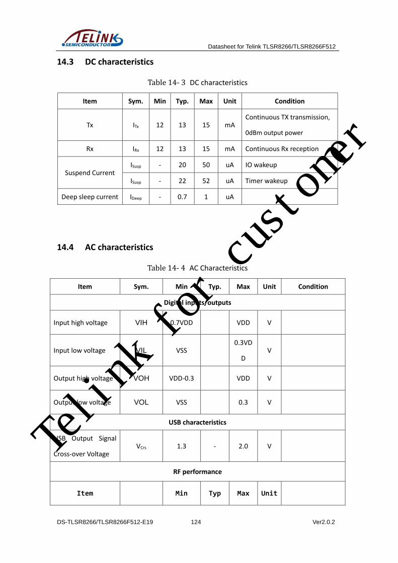
Datasheet for Telink TLSR8266/TLSR8266F512
DS-TLSR8266/TLSR8266F512-E19 124 Ver2.0.2
14.3 DC characteristics
Table 14- 3 DC characteristics
Item Sym. Min Typ. Max Unit Condition
Tx ITx 12 13 15 mA Continuous TX transmission,
0dBm output power
Rx IRx 12 13 15 mA Continuous Rx reception
Suspend Current ISusp - 20 50 uA IO wakeup
ISusp - 22 52 uA Timer wakeup
Deep sleep current IDeep - 0.7 1 uA
14.4 AC characteristics
Table 14- 4 AC Characteristics
Item Sym. Min Typ. Max Unit Condition
Digital inputs/outputs
Input high voltage VIH 0.7VDD
VDD V
Input low voltage VIL VSS
0.3VD
D V
Output high voltage VOH VDD-0.3
VDD V
Output low voltage VOL VSS
0.3 V
USB characteristics
USB Output Signal
Cross-over Voltage VCrs 1.3 - 2.0 V
RF performance
Item
Min Typ Max Unit
Telink for customer

Datasheet for Telink TLSR8266/TLSR8266F512
DS-TLSR8266/TLSR8266F512-E19 125 Ver2.0.2
Item Sym. Min Typ. Max Unit Condition
RF_Rx performance
Sensitivity 1Mbps -93 -92 -90 dBm
Frequency Offset
Tolerance -300 +300 KHz
Co-channel rejection -7 dB
In-band blocking
rejection
±1 MHz
offset 12 dB
-2 MHz
offset 47 dB
+2 MHz
offset 40 dB
-3 MHz
offset 48 dB
+3 MHz
offset 50 dB
>4MHz
offset 52 dB
Image rejection 44 dB
RF_Tx performance
Output power 8 dBm
Modulation 20dB
bandwidth 1000 KHz
12MHz/16MHz crystal
Nominal frequency
(parallel resonant) fNOM
12
MHz
Telink for customer
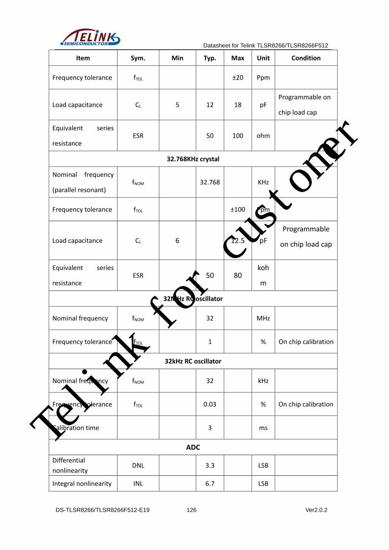
Datasheet for Telink TLSR8266/TLSR8266F512
DS-TLSR8266/TLSR8266F512-E19 126 Ver2.0.2
Item Sym. Min Typ. Max Unit Condition
Frequency tolerance fTOL
±20 Ppm
Load capacitance CL 5 12 18 pF Programmable on
chip load cap
Equivalent series
resistance ESR
50 100 ohm
32.768KHz crystal
Nominal frequency
(parallel resonant) fNOM
32.768 KHz
Frequency tolerance fTOL
±100 Ppm
Load capacitance CL 6 12.5 pF
Programmable
on chip load cap
Equivalent series
resistance ESR
50 80
koh
m
32MHz RC oscillator
Nominal frequency fNOM
32
MHz
Frequency tolerance fTOL
1
% On chip calibration
32kHz RC oscillator
Nominal frequency fNOM
32
kHz
Frequency tolerance fTOL
0.03
% On chip calibration
Calibration time
3
ms
ADC
Differential
nonlinearity DNL 3.3 LSB
Integral nonlinearity INL 6.7 LSB
Telink for customer

Datasheet for Telink TLSR8266/TLSR8266F512
DS-TLSR8266/TLSR8266F512-E19 127 Ver2.0.2
Item Sym. Min Typ. Max Unit Condition
Signal-to-noise and
distortion ratio
(fin=1kHz, fS=16kHz)
SINAD 56 dB
Spurious free
dynamic range
(fin=1kHz, fS=16kHz)
SFDR 63 dB
Effective Number of
Bits ENOB 10.5 bits
Sampling frequency Fs 250 KHz AVDD reference
200 KHz 1.4V reference
Telink for customer

Datasheet for Telink TLSR8266/TLSR8266F512
DS-TLSR8266/TLSR8266F512-E19 128 Ver2.0.2
15 Applications
15.1 Application example for the TLSR8266ET48
15.1.1 Schematic
Telink for customer

Datasheet for Telink TLSR8266/TLSR8266F512
DS-TLSR8266/TLSR8266F512-E19 129 Ver2.0.2
Figure 15-1 Schematic for the TLSR8266ET48
Telink for customer

Datasheet for Telink TLSR8266/TLSR8266F512
DS-TLSR8266/TLSR8266F512-E19 130 Ver2.0.2
15.1.2 Layout
Figure 15-2 Layout for the TLSR8266ET48
Telink for customer
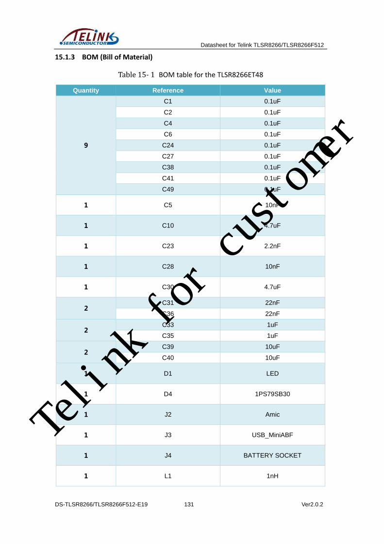
Datasheet for Telink TLSR8266/TLSR8266F512
DS-TLSR8266/TLSR8266F512-E19 131 Ver2.0.2
15.1.3 BOM (Bill of Material)
Table 15- 1 BOM table for the TLSR8266ET48
Quantity Reference Value
9
C1 0.1uF
C2 0.1uF
C4 0.1uF
C6 0.1uF
C24 0.1uF
C27 0.1uF
C38 0.1uF
C41 0.1uF
C49 0.1uF
1 C5 10nF
1 C10 4.7uF
1 C23 2.2nF
1 C28 10nF
1 C30 4.7uF
2 C31 22nF
C36 22nF
2 C33 1uF
C35 1uF
2 C39 10uF
C40 10uF
1 D1 LED
1 D4 1PS79SB30
1 J2 Amic
1 J3 USB_MiniABF
1 J4 BATTERY SOCKET
1 L1 1nH
Telink for customer

Datasheet for Telink TLSR8266/TLSR8266F512
DS-TLSR8266/TLSR8266F512-E19 132 Ver2.0.2
Quantity Reference Value
1 L4 BEAD_600
1 L9 2.2nH
2 Q2 PMOS_SI2301
Q9 PMOS_SI2301
2 R1 4.7K
R8 4.7K
2 R2 3.3K
R7 3.3K
1 R3 100K
1 R11 0
1 R12 2K
2 R13 2.2K
R15 2.2K
1 R14 2M
2 R17 1M
R67 1M
1 R51 1K
2
R69 33
R70 33
1 R71 10K
20
SW1 SW2PIN_2.2x4.0
SW2 SW2PIN_2.2x4.0
SW3 SW2PIN_2.2x4.0
SW4 SW2PIN_2.2x4.0
SW5 SW2PIN_2.2x4.0
SW6 SW2PIN_2.2x4.0
SW7 SW2PIN_2.2x4.0
SW8 SW2PIN_2.2x4.0
SW9 SW2PIN_2.2x4.0
SW11 SW2PIN_2.2x4.0
SW12 SW2PIN_2.2x4.0
Telink for customer

Datasheet for Telink TLSR8266/TLSR8266F512
DS-TLSR8266/TLSR8266F512-E19 133 Ver2.0.2
Quantity Reference Value
SW13 SW2PIN_2.2x4.0
SW15 SW2PIN_2.2x4.0
SW16 SW2PIN_2.2x4.0
SW17 SW2PIN_2.2x4.0
SW19 SW2PIN_2.2x4.0
SW20 SW2PIN_2.2x4.0
SW21 SW2PIN_2.2x4.0
SW23 SW2PIN_2.2x4.0
SW24 SW2PIN_2.2x4.0
1 U2 GD25Q40B/20B
1 U3 TLSR8266ET48
1 U4 CE3150
1 U5 XC6219_3.3V_SOT-23-5
1 U7 MPU6050
1 Y1 12MHZ
Telink for customer