datasheet - intersil · pdf filex9440 fn8200 rev 0.00 page 4 of 21 march 28, 2005 registers...
TRANSCRIPT

FN8200Rev 0.00
March 28, 2005
X9440 Mixed Signal with SPI Interface Dual Digitally Controlled Potentiometer (XDCP™) & Voltage Comparator
DATASHEET
FEATURES
• Two digitally controlled potentiometers and two voltage comparators in one package
• SPI serial interface • Register oriented format
—Direct read/write wiper position—Store as many as four positions per pot
• Fast response comparator• Enable, latch, or shutdown comparator outputs
through the ACR• Auto-recall of WCR and ACR data from R0• Hardware write protection, WP• Separate analog and digital/system supplies• Direct write cell
—Endurance–100,000 data changes per bit per register
—Register data retention–100 years• 16-bytes of EEPROM memory• Power saving feature and low noise• Two 10k or two 2.5k potentiometers• Resolution: 64 taps each pot• 24-lead TSSOP and 24-Lead SOIC packages
DESCRIPTION
The X9440 integrates two non volatile digitally con-trolled potentiometers (XDCP) and two voltage com-parators on a CMOS monolithic microcircuit.
The X9440 contains two resistor arrays, each com-posed of 63 resistive elements. Between each ele-ment and at either end are tap points accessible to thewiper elements. The position of the wiper element onthe array is controlled by the user through the SPIserial bus interface.
Each potentiometer has an associated voltage com-parator. The comparator compares the external inputvoltage VNI with the wiper voltage VW and sets the out-put voltage level to a logic high or low.
Each resistor array and comparator has associatedwith it a wiper counter register (WCR), analog controlregister (ACR), and eight 6 bit data registers that canbe directly written and read by the user. The contentsof the wiper counter register controls the position ofthe wiper on the resistor array. The contents of theanalog control register controls the comparator and itsoutput. The potentiometer is programmed with a SPIserial interface.
BLOCK DIAGRAM
VOUT (0,1)
(R0-R3)0,1
Interfaceand
ControlCircuitry
SCKS0SI
A1CS
HOLD
VH (0,1)
VL (0,1)WP
VW (0,1)
VNI (0,1)
+
–
WCR0,1
(R0-R3)0,1 ACR0,1
A0
FN8200 Rev 0.00 Page 1 of 21March 28, 2005

X9440
PIN DESCRIPTIONS
Host Interface Pins
Serial Output (SO)
SO is a push/pull serial data output pin. During a readcycle, data is shifted out on this pin. Data is clocked outby the falling edge of the serial clock.
Serial Input (SI)
SI is the serial data input pin. All opcodes, byteaddresses and data to be written to the pots and pot reg-isters are input on this pin. Data is latched by the risingedge of the serial clock.
Serial Clock (SCK)
The SCK input is used to clock data into and out of theX9440.
Chip Select (CS)
When CS is HIGH, the X9440 is deselected and the SOpin is at high impedance, and (unless an internal writecycle is underway) the device will be in the standbystate. CS LOW enables the X9440, placing it in theactive power mode. It should be noted that after apower-up, a HIGH to LOW transition on CS is requiredprior to the start of any operation.
Hold (HOLD)
HOLD is used in conjunction with the CS pin to selectthe device. Once the part is selected and a serialsequence is underway, HOLD may be used to pause theserial communication with the controller without resettingthe serial sequence. To pause, HOLD must be broughtLOW while SCK is LOW. To resume communication,HOLD is brought HIGH, again while SCK is LOW. If thepause feature is not used, HOLD should be held HIGHat all times.
Device Address (A0-A1)
The address inputs are used to set the least significant 2bits of the 8-bit slave address. A match in the slaveaddress serial data stream must be made with theAddress input in order to initiate communication with theX9440. A maximum of 4 devices may share the sameSPI serial bus.
Potentiometer Pins
VH (VH0-VH3), VL (VL0-VL3)The VH and VL inputs are equivalent to the terminal con-nections on either end of a mechanical potentiometer.
VW (VW0-VW1)
The wiper output VW is equivalent to the wiper output ofa mechanical potentiometer and is connected to theinverting input of the voltage comparator.
Comparator and Device Pins
Voltage Input VNI0, VNI1
VNI0 and VNI1 are the input voltages to the plus (non-inverting) inputs of the two comparators.
Buffered Voltage Outputs VOUT0, VOUT1
VOUT0 and VOUT1 are the buffered voltage comparatoroutputs controlled by bits in the volatile analog controlregister.
Hardware Write Protect Input WP
The WP pin when low prevents non volatile writes to thewiper counter and analog control registers.
Analog Supplies V+, V-
The Analog Supplies V+, V- are the supply voltages forthe XDCP analog section and the voltage comparators.
System Supply VCC and Ground VSS
The system supply, VCC and its reference VSS is used tobias the interface and control circuits.
FN8200 Rev 0.00 Page 2 of 21March 28, 2005

X9440
PIN CONFIGURATION
PIN NAMES
PRINCIPLES OF OPERATION
The X9440 is a highly integrated microcircuit incorporat-ing two resistor arrays, two voltage comparators andtheir associated registers and counters; and the serialinterface logic providing direct communication betweenthe host and the digitally-controlled potentiometers andvoltage comparators.
Serial Interface
The X9440 supports the SPI interface hardware conven-tions. The device is accessed via the SI input with dataclocked in on the rising SCK. CS must be LOW and theHOLD and WP pins must be HIGH during the entireoperation.
The SO and SI pins can be connected together, sincethey have three state outputs. This can help to reducesystem pin count.
Array Description
The X9440 is comprised of two resistor arrays and twovoltage comparators. Each array contains 63 discreteresistive segments that are connected in series. Thephysical ends of each array are equivalent to the fixedterminals of a mechanical potentiometer (VH and VLinputs).
At both ends of each array and between each resistorsegment is a CMOS switch connected to the wiper (VW)output. Within each individual array only one switch maybe turned on at a time. These switches are controlled bya volatile wiper counter register (WCR). The six bits ofthe WCR are decoded to select, and enable, one ofsixty-four switches.
The WCR may be written directly, or it can be changedby transferring the contents of one of four associateddata registers into the WCR. These data registers andthe WCR can be read and written by the host system.
Voltage Comparator
The comparator compares the wiper voltage VW with theexternal input voltage VNI. The comparator and its logiclevel output are controlled by the shutdown, latch, andenable bits of the analog control register (ACR). Enableconnects the comparator output to the VOUT pin, Latchmemorizes the output logic state, and shutdownremoves the analog section supply voltages to savepower. The analog control register (ACR) is pro-grammed using the SPI serial interface.
The ACR may be written directly, or it can be changedby transferring the contents of one of four associateddata registers into the ACR. These data registers andthe ACR may be read and written by the host system.
Symbol Description
SCK Serial Clock
S1, SO Serial Data
A0-A1 Device Address
VH0-VH1, VL0-VL1
Potentiometers (terminal equivalent)
VW0–VW1 Potentiometers (wiper equivalent)
VNI0, VNI1 Comparator Input Voltages
VOUT0, VOUT1 Buffered Comparator Outputs
WP Hardware Write Protection
V+,V- Analog and Voltage Comparator Supplies
VCC System Supply Voltage
VSS System Ground
NC No Connection
VCCVL0VH0
WPSI
A1
12345678910
24232221201918171615
V+VOUT0VNI0
NCA0SOHOLDSCKNCVNI1
SOIC
X9440
VSS
VW0
1413
11
12
CS
VL1
VH1VW1 VOUT1
V-
123456789
10
24232221201918171615
TSSOP
X9440
14
13
1112
SIA1
VL1
VH1VW1VSS
NCV- V+
VOUT1 VOUT0
SCK
HOLD
VNI1 VNI0
S0
A0
VCCNC
VL0
VH0
VW0
WPCS
FN8200 Rev 0.00 Page 3 of 21March 28, 2005

X9440
REGISTERS
Both digitally-controlled potentiometers and voltage com-parators share the serial interface and share a commonarchitecture. Each potentiometer and voltage comparatoris associated with wiper counter and analog control regis-ters and eight data registers. A detailed discussion of theregister organization and array operation follows.
Wiper Counter (WCR) and Analog Control Registers (ACR)
The X9440 contains two wiper counter registers: one foreach XDCP potentiometer and two Analog Control Reg-isters, and one for each of the two voltage comparators.The wiper counter register is equivalent to a serial-in,parallel-out counter with its outputs decoded to selectone of sixty-four switches along its resistor array. Thecontents of the wiper counter register and analog controlregister can be altered in four ways: it may be writtendirectly by the host via the Write WCR instruction (serialload); it may be written indirectly by transferring the con-tents of one of four associated data registers (DR) viathe XFR data register instruction (parallel load); it can bemodified one step at a time by the increment/ decrementinstruction (WCR only). Finally, it is loaded with the con-tents of its data register zero (R0) upon power-up.
The wiper counter and analog control register are vola-tile registers; that is, their contents are lost when theX9440 is powered-down. Although the registers areautomatically loaded with the value in R0 upon power-up, it should be noted this may be different from thevalue present at power-down.
Programming the ACR is similar to the WCR. However,the 6 bits in the WCR positions the wiper in the resistorarray while 3 bits in the ACR control the comparator andits output.
Data Registers (DR)
Each potentiometer and each voltage comparator hasfour non volatile data registers (DR). These can be reador written directly by the host and data can be trans-ferred between any of the four data registers and theWCR or ACR. It should be noted all operations changingdata in one of these registers is a non volatile operationand will take a maximum of 10ms.
If the application does not require storage of multiple set-tings for the potentiometer or comparator, these registerscan be used as regular memory locations that could storesystem parameters or user preference data.
Figure 1. Detailed Potentiometer Block Diagram
Serial Data Path
From InterfaceCircuitry
Register 0 Register 1
Register 2 Register 3
SerialBusInput
ParallelBusInput
CounterRegister
Inc/DecLogic
UP/DN
CLKModified SCK
UP/DN
VH
VL
VW
8 6
Counter
Decode
If WC = 00[H] VW = VLIf WC = 3F[H] VW = VH
Wiper
(One of Two Arrays)
(WCR)
FN8200 Rev 0.00 Page 4 of 21March 28, 2005

X9440
REGISTER BIT DESCRIPTIONS
Wiper Counter Register (WCR)
WP0-WP5 identify wiper position.
Analog Control Register (ACR)
Shutdown
“1” indicates power is connected to the voltagecomparator.
“0” indicates power is not connected to the voltagecomparator.
Enable
“1” indicates the output buffer of the voltagecomparator is enabled.
“0” indicates the output buffer of the voltagecomparator is disabled.
Latch
“1” indicates the output of the voltage comparator ismemorized or latched.
“0” indicates the output of the voltage comparator isnot latched.
Userbits—available for user applications
Data Registers (DR, R0-R3)
{Refer to Memory Map, Figure 9}
INSTRUCTIONS AND PROGRAMMING
Identification (ID) Byte
The first byte sent to the X9440 from the host, followinga CS going HIGH to LOW, is called the Identificationbyte. The most significant four bits of the slave addressare a device type identifier, for the X9440 this is fixed as0101[B] (refer to Figure 2).
The two least significant bits in the ID byte select one offour devices on the bus. The physical device address isdefined by the state of the A0-A1 input pins. The X9440compares the serial data stream with the address inputstate; a successful compare of both address bits isrequired for the X9440 to successfully continue the com-mand sequence. The A0-A1 inputs can be actively drivenby CMOS input signals or tied to VCC or VSS.
The remaining two bits in the slave byte must be set to 0.
Figure 2. Identification Byte Format
Instruction Byte
The byte following the address contains the instructionand register pointer information. The four most signifi-cant bits are the instruction. The next four bits point toone of the two pots or two voltage comparators andwhen applicable they point to one of four associated reg-isters. The format is shown below in Figure 3.
Figure 3. Instruction Byte Format
The four high order bits of the instruction byte specify theoperation. The next two bits (R1 and R0) select one ofthe four data registers that is to be acted upon when aregister oriented instruction is issued. The last two bits(P1 and P0) selects which one of the four potentiometersis to be affected by the instruction.
The four high order bits define the instruction. The next twobits (R1 and R0) select one of the four data registers that isto be acted upon when a register oriented instruction isissued. The last two bits (P1 and P0) select which one ofthe two potentiometers or which one of the two voltagecomparators is to be affected by the instruction.
0 0 WP5 WP4 WP3 WP2 WP1 WP0
(volatile) (LSB)
0 0User-bit5
User-bit4
User-bit3 Latch Enable
Shut-down
(volatile) (LSB)
Wiper Position or Analog Control Data or User Data
(Nonvolatile)
10 0 0 0 A1 A0
Device TypeIdentifier
Device Address
1
I1I2I3 I0 R1 R0 P1 P0
Pot Select
RegisterSelect
Instructions
FN8200 Rev 0.00 Page 5 of 21March 28, 2005

X9440
Four of the ten instructions end with the transmission ofthe instruction byte. The basic sequence is illustrated inFigure 4. These two-byte instructions exchange databetween the wiper counter register or analog control reg-ister and one of the data registers. A transfer from a dataregister to a wiper counter register or analog control reg-ister is essentially a write to a static RAM. The responseof the wiper to this action will be delayed tWRL. A transferfrom the wiper counter register current wiper position toa data register is a write to non volatile memory andtakes a minimum of tWR to complete. The transfer canoccur between one of the two potentiometers or one ofthe two voltage comparators and one of its associatedregisters; or it may occur globally, wherein the transferoccurs between both of the potentiometers and voltagecomparators and one of their associated registers.
Five instructions require a three-byte sequence to com-plete. These instructions transfer data between the hostand the X9440; either between the host and one of thedata registers or directly between the host and the wipercounter and analog control registers. These instructionsare: Read Wiper Counter Register or Analog ControlRegister, read the current wiper position of the selectedpot or the comparator control bits, Write Wiper CounterRegister or Analog Control Register, i.e. change currentwiper position of the selected pot or control the voltagecomparator; Read Data Register, read the contents of theselected non volatile register; Write Data Register, write anew value to the selected data register. The bit structuresof the instructions are shown in Figure 9.
The sequences of the three byte operations are shownin Figure 5 and Figure 6.
The bit structures of the instructions and the descriptionof the instructions are shown in Figure 10.
Figure 4. Two-Byte Command Sequence
Figure 5. Three-Byte Command Sequence (Write)
0 1 0 1 0 0 A1 A0 I3 I2 I1 I0 R1 R0 P1 P0
SCK
SI
CS
0 1 0 1 A1 A0 I3 I2 I1 I0 R1 R0 P1 P0
SCL
SI
0 0 D5 D4 D3 D2 D1 D0
CS
0 0
FN8200 Rev 0.00 Page 6 of 21March 28, 2005

X9440
Figure 6. Three-Byte Command Sequence (Read)
Figure 7. Increment/Decrement Command Sequence
Increment/Decrement
The final command is Increment/Decrement. It is differentfrom the other commands, because it’s length is indeter-minate. Once the command is issued, the master canclock the selected wiper up and/or down in one resistorsegment steps; thereby, providing a fine tuning capabilityto the host. For each SCK clock pulse (tHIGH) while SI isHIGH, the selected wiper will move one resistor segmenttowards the VH terminal. Similarly, for each SCK clockpulse while SI is LOW, the selected wiper will move one
resistor segment towards the VL terminal. A detailed illus-tration of the sequence and timing for this operation areshown in Figure 7 and 8.
Write in Process
The contents of the data registers are saved to nonvola-tile memory when the CS pin goes from LOW to HIGHafter a complete write sequence is received by thedevice. The progress of this internal write operation canbe monitored by a write in process bit (WIP). The WIP bitis read with a read status command.
Figure 8. Increment/Decrement Timing Limits
0 1 0 1 A1 A0 I3 I2 I1 I0 R1 R0 P1 P0
SCL
SI
CS
0 0
S0
0 0 D5 D4 D3 D2 D1 D0
Don’t Care
0 1 0 1 0 0 A1 A0 I3 I2 I1 I0 0 P1 P0
SCK
SI
INC1
INC2
INCn
DEC1
DECn
0
CS
SCK
SI
VW
INC/DEC CMD Issued
Voltage Out
tWRID
FN8200 Rev 0.00 Page 7 of 21March 28, 2005
X9440
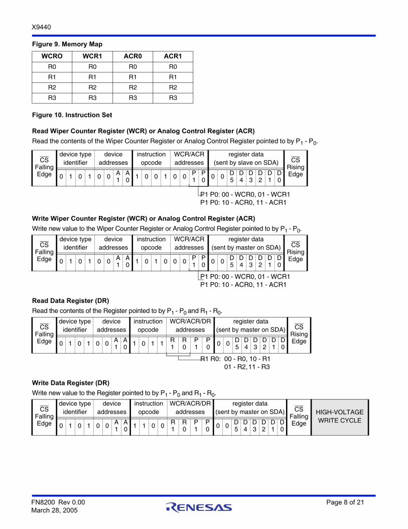
Figure 9. Memory Map
Figure 10. Instruction Set
Read Wiper Counter Register (WCR) or Analog Control Register (ACR)
Read the contents of the Wiper Counter Register or Analog Control Register pointed to by P1 - P0.
P1 P0: 00 - WCR0, 01 - WCR1P1 P0: 10 - ACR0, 11 - ACR1
Write Wiper Counter Register (WCR) or Analog Control Register (ACR)
Write new value to the Wiper Counter Register or Analog Control Register pointed to by P1 - P0.
P1 P0: 00 - WCR0, 01 - WCR1P1 P0: 10 - ACR0, 11 - ACR1
Read Data Register (DR)
Read the contents of the Register pointed to by P1 - P0 and R1 - R0.
R1 R0: 00 - R0, 10 - R101 - R2,11 - R3
Write Data Register (DR)
Write new value to the Register pointed to by P1 - P0 and R1 - R0.
WCRO WCR1 ACR0 ACR1
R0 R0 R0 R0
R1 R1 R1 R1
R2 R2 R2 R2
R3 R3 R3 R3
CS Falling Edge
device typeidentifier
deviceaddresses
instructionopcode
WCR/ACRaddresses
register data(sent by slave on SDA) CS
Rising Edge0 1 0 1 0 0 A
1A0 1 0 0 1 0 0 P
1P0 0 0 D
5D4
D3
D2
D1
D0
CS Falling Edge
device typeidentifier
deviceaddresses
instructionopcode
WCR/ACRaddresses
register data(sent by master on SDA) CS
Rising Edge0 1 0 1 0 0 A
1A0 1 0 1 0 0 0 P
1P0 0 0 D
5D4
D3
D2
D1
D0
CS Falling Edge
device typeidentifier
deviceaddresses
instructionopcode
WCR/ACR/DRaddresses
register data(sent by master on SDA) CS
Rising Edge0 1 0 1 0 0 A
1A0 1 0 1 1 R
1R0
P1
P0 0 0 D
5D4
D3
D2
D1
D0
CS Falling Edge
device typeidentifier
deviceaddresses
instructionopcode
WCR/ACR/DRaddresses
register data(sent by master on SDA) CS
Falling Edge
HIGH-VOLTAGEWRITE CYCLE
0 1 0 1 0 0 A1
A0 1 1 0 0 R
1R0
P1
P0 0 0 D
5D4
D3
D2
D1
D0
FN8200 Rev 0.00 Page 8 of 21March 28, 2005

X9440
Transfer Data Register to Wiper Counter Register or Analog Control Register
Transfer the contents of the Register pointed to by R1 - R0 to the WCR or ACR pointed to by P1 - P0.
Transfer Wiper Counter or Analog Control Register to Data Register
Transfer the contents of the WCR or ACR pointed to by P1 - P0 to the Register pointed to by R1 - R0.
Global Transfer Data Register to Wiper Counter or Analog Control Register
Transfer the contents of all four Data Registers pointed to by R1 - R0 to their respective WCR or ACR.
Global Transfer Wiper Counter or Analog Control Register to Data Register
Transfer the contents of all WCRs and ACRs to their respective data Registers pointed to by R1 - R0.
Increment/Decrement Wiper Counter Register
Enable Increment/decrement of the WCR pointed to by P1 - P0.
P1 P0: 00 or 01 only.I/D: Increment/Decrement, 1/0
Read Status
CS Falling Edge
device typeidentifier
deviceaddresses
instructionopcode
WCR/ACR/DRaddresses CS
Rising Edge0 1 0 1 0 0 A
1A0 1 1 0 1 R
1R0
P1
P0
CS Falling Edge
device typeidentifier
deviceaddresses
instructionopcode
WCR/ACR/DRaddresses CS
Rising Edge
HIGH-VOLTAGEWRITE CYCLE
0 1 0 1 0 0 A1
A0 1 1 1 0 R
1R0
P1
P0
CS Falling Edge
device typeidentifier
deviceaddresses
instructionopcode
DRaddresses CS
Rising Edge0 1 0 1 0 0 A
1A0 0 0 0 1 R
1R0 0 0
CS Falling Edge
device typeidentifier
deviceaddresses
instructionopcode
DRaddresses CS
Rising Edge
HIGH-VOLTAGEWRITE CYCLE
0 1 0 1 0 0 A1
A0 1 0 0 0 R
1R0 0 0
CS Falling Edge
device typeidentifier
deviceaddresses
instructionopcode
WCRaddresses
increment/decrement(sent by master on SDA) CS
Rising Edge0 1 0 1 0 0 A
1A0 0 0 1 0 0 0 P
1P0
I/D
I/D . . . . I/
DI/D
CS Falling Edge
device typeidentifier
deviceaddresses
instructionopcode
wiperaddresses
Data Byte(sent by X9440 on SO) CS
Rising Edge0 1 0 1 0 0 A
1A0 0 1 0 1 0 0 0 1 0 0 0 0 0 0 0
WIP
FN8200 Rev 0.00 Page 9 of 21March 28, 2005

X9440
ABSOLUTE MAXIMUM RATINGS
Temperature under bias .................... -65°C to +135°CStorage temperature ......................... -65°C to +150°CVoltage on SCK, SCL or any address input
with respect to VSS.................................. -1V to +7VVoltage on V+ (referenced to VSS) ........................+7VVoltage on V- (referenced to VSS) ..........................-7V(V+) - (V-) ..............................................................12VAny VH.....................................................................V+Any VL ......................................................................V-Lead temperature (soldering, 10 seconds)........ 300°C
COMMENT
Stresses above those listed under “Absolute MaximumRatings” may cause permanent damage to the device.This is a stress rating only; functional operation of thedevice (at these or any other conditions above thoselisted in the operational sections of this specification) isnot implied. Exposure to absolute maximum rating condi-tions for extended periods may affect device reliability.
ANALOG CHARACTERISTICS (Over recommended operating conditions unless otherwise stated.)
Notes: (1) Absolute linearity is utilized to determine actual wiper voltage versus expected voltage as determined by wiper position when used as apotentiometer.
(2) Relative linearity is utilized to determine the actual change in voltage between two successive tap positions when used as a potentiom-eter. It is a measure of the error in step size.
(3) MI = RTOT/63 or (VH - VL)/63, single pot(4) Individual array resolutions.
RECOMMENDED OPERATING CONDITIONS
Temperature Min. Max.
Commercial 0°C +70°C
Industrial -40°C +85°C
Military -55°C +125°C
Device Supply Voltage (VCC) Limits
X9440 5V 10%
X9440-2.7 2.7V to 5.5V
Symbol Parameter
Limits
Test ConditionsMin. Typ. Max. Unit
RTOTAL End to end resistance –20 +20 %
Power rating 50 mW 25C, each pot
IW Wiper current –3 +3 mA
RW Wiper resistance 40 100 VCC = 5V, Wiper Current = 3mA
100 250 VCC = 2.7-5V, Wiper Current = 3mA
Vv+ Voltage on V+ pin X9440 +4.5 +5.5 V
X9440-2.7 +2.7 +5.5
Vv- Voltage on V- pin X9440 -5.5 -4.5 V
X9440-2.7 -5.5 -2.7
VTERM Voltage on any VH or VL pin V- V+ V
Noise -120 dBV Ref: 1kHz
Resolution (4) 1.6 %
Absolute linearity (1) -1 +1 MI(3) Vw(n)(actual) - Vw(n)(expected)
Relative linearity (2) -0.2 +0.2 MI(3) Vw(n + 1 - [Vw(n) + MI]
Temperature coefficient of RTOTAL 300 ppm/C
FN8200 Rev 0.00 Page 10 of 21March 28, 2005

X9440
COMPARATOR ELECTRICAL CHARACTERISTICS (Over the recommended operating conditions unless otherwise specified.)
Notes: (1) 100mV step with 100mV overdrive, ZL = 10k || 15pF, 10-90% risetime(2) Time from leading edge of Enable bit to valid VOUT.
Symbol Parameter
Limits
Unit Test ConditionsMin. Typ. Max.
VOS Input offset voltage -1-5
15
mVmV
V+/V- = 3VV+/V- = 5V
IB Input current 10 pA
VIR Input voltage range V- V+ V
tR Response time 200 ns note 1
IO Output current -1 1 mA
AV Voltage gain 300 V/mV
PSRR Power supply rejection ratio 60 dB
VOR Output voltage range VSS VCC V
TCVOS Input offset voltage drift 6 µV/°C
IS Supply current (V+ to V-) 1.2.5
mAmA
V+/V- = 5VV+/V- = 3V
TON Comparator enable time 1 µs note 2
VOL Output low voltage 0.4 V IO = 1mA
VOH Output high voltage VCC-0.8 V IO = 1mA
FN8200 Rev 0.00 Page 11 of 21March 28, 2005

X9440
D.C. OPERATING CHARACTERISTICS (Over the recommended operating conditions unless otherwise specified.)
ENDURANCE AND DATA RETENTION
CAPACITANCE
POWER-UP SEQUENCE
A.C. TEST CONDITIONS
Note: (1) Applicable to recall and power consumption applications
EQUIVALENT A.C. LOAD CIRCUIT
Symbol Parameter
Limits
Test ConditionsMin. Typ. Max. Unit
ICC1 VCC supply current (active) 400 µA fSCK = 2MHz, SO = Open, Other Inputs = VSS
ICC2 VCC supply current (nonvolatile write)
1 mA fSCK = 2MHz, SO = Open, Other Inputs = VSS
ISB VCC current (standby) 1 µA SCK = SI = VSS, Addr. = VSS
ILI Input leakage current 10 µA VIN = VSS to VCC
ILO Output leakage current 10 µA VOUT = VSS to VCC
VIH Input HIGH voltage VCC x 0.7 VCC + 0.5 V
VIL Input LOW voltage -0.5 VCC x 0.1 V
VOL Output LOW voltage 0.4 V IOL = 3mA
Parameter Min. Unit
Minimum endurance 100,000 Data changes per bit per register
Data retention 100 Years
Symbol Test Max. Unit Test Conditions
CI/O Output capacitance (SO) 8 pF VOUT = 0V
CIN Input capacitance (A0, A1, SI, and SCK) 6 pF VIN = 0V
CL, CH, CW Potentiometer capacitance 10/10/25 pF
Power-up Sequence(1): (1) VCC (2) V+ and V- {V+ VCC at all times}
Power-down Sequence: no limitation
Input pulse levels VCC x 0.1 to VCC x 0.9
Input rise and fall times 10ns
Input and output timing level VCC x 0.5
5V
1533
100pF
SDA Output
2.7V
100pF
FN8200 Rev 0.00 Page 12 of 21March 28, 2005

X9440
AC TIMING
HIGH-VOLTAGE WRITE CYCLE TIMING
XDCP TIMING
Symbol Parameter Min. Max. Unit
fSCK SSI/SPI clock frequency 2.0 MHz
tCYC SSI/SPI clock cycle time 500 ns
tWH SSI/SPI clock high time 200 ns
tWL SSI/SPI clock low time 200 ns
tLEAD Lead time 250 ns
tLAG Lag time 250 ns
tSU SI, SCK, HOLD and CS input setup time 50 ns
tH SI, SCK, HOLD and CS input hold time 50 ns
tRI SI, SCK, HOLD and CS input rise time 2 µs
tFI SI, SCK, HOLD and CS input fall time 2 µs
tDIS SO output disable time 0 500 ns
tV SO output valid time 100 ns
tHO SO output hold time 0 ns
tRO SO output rise time 50 ns
tFO SO output fall time 50 ns
tHOLD HOLD time 400 ns
tHSU HOLD setup time 100 ns
tHH HOLD hold time 100 ns
tHZ HOLD low to output in high Z 100 ns
tLZ HOLD high to output in low Z 100 ns
TI Noise suppression time constant at SI, SCK, HOLD and CS inputs
20 ns
tCS CS Deselect Time 2 µs
tWPASU WP, A0 and A1 setup time 0 ns
tWPAH WP, A0 and A1 hold time 0 ns
Symbol Parameter Typ. Max. Unit
tWR High-voltage write cycle time (store instructions) 5 10 ms
Symbol Parameter Min. Max. Unit
tWRPO Wiper response time after the third (last) power supply is stable 10 µs
tWRL Wiper response time after instruction issued (all load instructions) 10 µs
tWRID Wiper response time from an active SCL/SCK edge (increment/decrement instruction) 450 µs
FN8200 Rev 0.00 Page 13 of 21March 28, 2005

X9440
SYMBOL TABLE
TIMING DIAGRAMS
Input Timing
Output Timing
WAVEFORM INPUTS OUTPUTS
Must besteady
Will besteady
May changefrom Low toHigh
Will changefrom Low toHigh
May changefrom High toLow
Will changefrom High toLow
Don’t Care:ChangesAllowed
Changing:State NotKnown
N/A Center Lineis HighImpedance
...
CS
SCK
SI
SO
MSB LSB
High Impedance
tLEAD
tHtSUtFI
tCS
tLAGtCYC
tWL
...
tRItWH
...
CS
SCK
SO
SI ADDR
MSB LSB
tDIStHOtV
...
FN8200 Rev 0.00 Page 14 of 21March 28, 2005

X9440
Hold Timing
XDCP Timing (for All Load Instructions)
XDCP Timing (for Increment/Decrement Instruction)
Write Protect and Device Address Pins Timing
...
CS
SCK
SO
SI
HOLD
tHSU tHH
tLZtHZ
tHOLD
tRO tFO
...
CS
SCK
SI MSB LSB
VWx
tWRL
...
SOHigh Impedance
...
CS
SCK
SO
SI ADDR
tWRID
High Impedance
VWx
...Inc/Dec Inc/Dec
...
CS
WP
A0
A1
tWPASU tWPAH
(Any Instruction)
FN8200 Rev 0.00 Page 15 of 21March 28, 2005

X9440
BASIC APPLICATIONS
+5V
VH V+SCL
SDA
VOUT
–
+
V–VLVSS
SCL
SDA
9440
VREF1 (+5V)
VTRANSDUCER (VT)
VWVOUT
Programmable Window Detector with Memory
SCL +
–
SDA
+
–
+5V
–5V
9440
VW0
VW1
VOUT0
VOUT1
VOUT0
VS
VLL VUL
(VW1) (VW0)
VT > VW, VOUT = High
VT < VW, VOUT = Low+
–
VOUT0 = LVOUT1 = L
VOUT0 = HVOUT1 = H
VOUT0 = LVOUT1 = H
For the signal voltage VS > the upper limit VUL, (VOUT0 = H) • (VOUT1 = H)VS < the lower limit VLL, (VOUT0 = L) • (VOUT1 = L)
For the window VLL VS VUL, (VOUT0 = L) • (VOUT1 = H)
VS
+
–
VCC
VNI
(+5V)
(-5V)
VREF2 (–5V)
Programmable Level Detector with Memory (typical bias conditions)
FN8200 Rev 0.00 Page 16 of 21March 28, 2005

X9440
BASIC APPLICATION (continued)
Programmable Oscillator with Memory
Programmable Schmitt Trigger with Memory
+5V
VH
V+
SCL
SDA–
+V–
VW
VOUT
Frequency R, C
VL
+5V
R2
R1R3
R
C
Duty Cycle R1, R2, R3
VH
V+–
+V–
VOUT
VL
R2R1
R
VS
VLL VUL
VOUT
VLL
R1 R2+
R2---------------------VW
R1R2-------VOUT max –=
VUL
R1 R2+
R2---------------------VW
R1R2-------VOUT min –=
VR
VW
VS
9440
9440
FN8200 Rev 0.00 Page 17 of 21March 28, 2005
X9440
BASIC APPLICATION (continued)
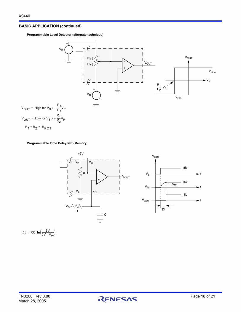
Programmable Level Detector (alternate technique)
Programmable Time Delay with Memory
–
+
VR
VOUT
+
+
R2
{
{
R1
VS
VOUT High for VS – R1R2-------VR=
VOUT Low for VS – R1R2-------VR=
R1 R2+ RPOT=
VOUT
VS
-R1R2
VR
VH
–
+
VL
VW
VOUT
VNI
VOUT
Dt
+5V
VS
RC
t RC ln 5V5V VW–----------------------- =
t
t
t
+5v
+5v
+5v
VS
VNI
VOUT
VW
VSS=
VCC
FN8200 Rev 0.00 Page 18 of 21March 28, 2005

X9440
PACKAGING INFORMATION
0.290 (7.37)0.299 (7.60)
0.393 (10.00)0.420 (10.65)
0.014 (0.35)0.020 (0.50)
Pin 1
Pin 1 Index
0.050 (1.27)
0.598 (15.20)0.610 (15.49)
0.003 (0.10)0.012 (0.30)
0.092 (2.35)0.105 (2.65)
(4X) 7°
24-Lead Plastic Small Outline Gull Wing Package Type S
NOTE: ALL DIMENSIONS IN INCHES (IN PARENTHESES IN MILLIMETERS)
0.420"
0.050" Typical
0.050" Typical
0.030" Typical 24 PlacesFOOTPRINT
0.010 (0.25)0.020 (0.50)
0.015 (0.40)0.050 (1.27)
0.009 (0.22)0.013 (0.33)
0° - 8°
X 45°
FN8200 Rev 0.00 Page 19 of 21March 28, 2005

X9440
PACKAGING INFORMATION
NOTE: ALL DIMENSIONS IN INCHES (IN PARENTHESES IN MILLIMETERS)
24-Lead Plastic, TSSOP Package Type V
.169 (4.3)
.177 (4.5).252 (6.4) BSC
.026 (.65) BSC
.303 (7.70)
.311 (7.90)
.002 (.06)
.005 (.15)
.047 (1.20)
.0075 (.19)
.0118 (.30)
See Detail “A”
.031 (.80).041 (1.05)
.010 (.25)
.020 (.50)
.030 (.75)
Gage Plane
Seating Plane
Detail A (20X)
(4.16) (7.72)
(1.78)
(0.42)(0.65)
ALL MEASUREMENTS ARE TYPICAL
0° - 8°
FN8200 Rev 0.00 Page 20 of 21March 28, 2005

X9440
Intersil products are manufactured, assembled and tested utilizing ISO9001 quality systems as notedin the quality certifications found at www.intersil.com/en/support/qualandreliability.html
Intersil products are sold by description only. Intersil may modify the circuit design and/or specifications of products at any time without notice, provided that such modification does not, in Intersil's sole judgment, affect the form, fit or function of the product. Accordingly, the reader is cautioned to verify that datasheets are current before placing orders. Information furnished by Intersil is believed to be accurate and reliable. However, no responsibility is assumed by Intersil or its subsidiaries for its use; nor for any infringements of patents or other rights of third parties which may result from its use. No license is granted by implication or otherwise under any patent or patent rights of Intersil or its subsidiaries.
For information regarding Intersil Corporation and its products, see www.intersil.com
For additional products, see www.intersil.com/en/products.html
© Copyright Intersil Americas LLC 2005. All Rights Reserved.All trademarks and registered trademarks are the property of their respective owners.
Ordering Information
Device VCC LimitsBlank = 5V 10%-2.7 = 2.7 to 5.5V
Temperature RangeBlank = Commercial = 0°C to +70°CI = Industrial = -40°C to +85°C
PackageP24 = 24-Lead Plastic DIPS24 = 24-Lead SOICV24 = 24-Lead TSSOP
Potentiometer OrganizationPot 0 Pot 1
W = 10k 10kY = 2.5k 2.5k
X9440 P T VY
FN8200 Rev 0.00 Page 21 of 21March 28, 2005