datasheet - ldl112 - 1.2 a low quiescent current ldo with ... · 4 maximum ratings table 2....
TRANSCRIPT

Features• Input voltage from 1.6 to 5.5 V• Very low-dropout voltage (300 mV typ. at 1 A load)• Low quiescent current (35 µA typ. at no-load, 1 µA max. in off mode)• Output voltage tolerance: ± 2.0% at 25 °C• 1.2 A guaranteed output current• Wide range of output voltages available on request: 0.8 V to 5 V with 50 mV
step and adjustable• Logic-controlled electronic shutdown• Compatible with ceramic capacitor COUT = 1 µF• Internal current and thermal limit• Available in DFN6 (2x2), DFN6 (3x3) mm, SO8-batwing and PPAK packages• Temperature range: -40 °C to 125 °C• Reverse current protection• Output discharge function (optional)
Applications• Consumer• Computer• Battery-powered systems• Low voltage point-of-load• USB-powered devices
DescriptionThe LDL112 is a low-dropout linear regulator, which can provide a maximum currentof 1.2 A, with a typical dropout voltage of 300 mV.
It is stabilized with a ceramic capacitor on the output.
The very low drop voltage, low quiescent current and reverse current protectionfeatures make it suitable for low power battery-powered applications.
The enable logic control function puts the LDL112 in shutdown mode allowing a totalcurrent consumption lower than 1 µA.
The device is equipped with current limit and thermal protection.
Maturity status link
LDL112
1.2 A low quiescent current LDO with reverse current protection
LDL112
Datasheet
DS10321 - Rev 3 - February 2019For further information contact your local STMicroelectronics sales office.
www.st.com

1 Diagram
Figure 2. Block diagram
800mV
PMOS
OPAMPVFB
EN Enable
Internal enable
Reverse current
protection
VOUT
VIN
Thermal protection
*
Current limit
GND
Bandgapreference
800mV
PMOS
OPAMPVFB
Bandgapreference
EN Enable
Internal enable
Reverse current
protection
VOUT
VIN
Thermal protection
*
Current limit
GND
ADJ
Fixed version Adjustable version
AM14036V1
Note: (*) The output discharge function is optional.
LDL112Diagram
DS10321 - Rev 3 page 2/32

2 Pin configuration
Figure 3. Pin connection DFN6 (3x3) and DFN6 (2x2) (top view)
Figure 4. Pin connection PPAK and SO8 (top view)
Table 1. Pin description
Symbol Function
VIN LDO input voltage
GND Common ground
EN Enable pin logic input: low = shutdown, high = active. Don't leave this pin floating
ADJ Adjustable pin (on adjustable version)
VOUT LDO output voltage
Exposed pad Must be connected to GND
NC Not connected
LDL112Pin configuration
DS10321 - Rev 3 page 3/32

3 Typical application
Figure 5. Typical application circuits
AM14039V1
Adjustable version
VIN
GND
VI
ENCIn
VOVOUT
COut
LDL112
OFF
ON
1µF 1µF
R1
R2
VIN
GND
VI
EN
CIn
VOVOUT
COut
LDL112OFF
ON
1µF 1µF
Fixed version
LDL112Typical application
DS10321 - Rev 3 page 4/32

4 Maximum ratings
Table 2. Absolute maximum ratings
Symbol Parameter Value Unit
VIN DC input voltage - 0.3 to 7 V
VOUT DC output voltage - 0.3 to VI + 0.3 V
VEN Enable input voltage - 0.3 to VI + 0.3 V
VADJ ADJ pin voltage 2 V
IOUT Output current Internally limited mA
PD Power dissipation Internally limited mW
TSTG Storage temperature range - 65 to 150 °C
TOP Operating junction temperature range - 40 to 125 °C
Note: Absolute maximum ratings are those values beyond which damage to the device may occur. Functionaloperation under these conditions is not implied. All values are referred to GND.
Table 3. Thermal data
Symbol Parameter DFN6 (3x3) DFN6 (2x2) SO8 PPAK Unit
RthJAThermal resistancejunction-ambient 55 65 55(1) 100 °C/W
RthJCThermal resistancejunction-case 10 15 20 8 °C/W
1. Considering 6 cm² of copper board heatsink.
LDL112Maximum ratings
DS10321 - Rev 3 page 5/32

5 Electrical characteristics
TJ = 25 °C, VIN = VOUT(NOM) + 0.5 V (for VOUT(NOM) ≤ 1 V, VIN = 2.1 V), CIN = COUT = 1 µF, IOUT = 5 mA, VEN =VIN, unless otherwise specified.
Table 4. LDL112 electrical characteristics (fixed version)
Symbol Parameter Test conditions Min. Typ. Max. Unit
VIN Operating input voltage 1.6 5.5 V
VOUT VOUT accuracyIOUT = 5 mA, TJ = 25 °C -2.0 2.0 %
IOUT = 5 mA, -40 °C < TJ < 125 °C -3.0 3.0 %
ΔVOUT Static line regulation (1) VOUT(NOM) + 0.5 V < VIN ≤ 5.5 V (2) 0.05 0.1 %/V
ΔVOUT Static load regulation IOUT = 0 mA to 1.2 A, VIN > 2.1 V 15 30 mV
VDROP Dropout voltage (3)
IOUT = 1 A, VOUT = 3.3 V 300
mVIOUT = 1.2 A,VOUT = 3.3 V
-40 °C < TJ < 125 °C350 600
eN Output noise voltage10 Hz to 100 kHz, IOUT = 10 mA
VOUT = 3.3 V135 µVRMS
SVR Supply voltage rejection
VIN = VOUT(NOM) + 0.5 V +/- VRIPPLE (2)
VRIPPLE = 0.2 V frequency = 1 kHz
IOUT = 10 mA
57 dB
IQ Quiescent current
IOUT = 0 mA, -40 °C < TJ <125 °C 35 70
µAIOUT = 1.2 A, VOUT(NOM) + 1 V,
-40 °C < TJ < 125 °C (2)250 400
VIN input current in off mode: VEN = GND 0.1 1
ISC Short-circuit current RL = 0, VIN > 2.1 V 1.4 2 A
VEN
Enable input logic lowVIN = VOUT(NOM) + 0.5 V to 5.5 V,
-40 °C < TJ < 125 °C (2)0.35
V
Enable input logic highVIN = VOUT(NOM) + 0.5 V to 5.5 V,
-40 °C < TJ < 125 °C (2)1.4
IEN Enable pin input current VEN = VIN 100 nA
TSHDNThermal shutdown 165
°CHysteresis 20
COUT Output capacitor Capacitance (see Section 7 Typicalperformance characteristics) 1 10 µF
1. Not applicable for Vout(nom) > 4.5 V.
2. For VOUTNOM lower than or equal to 1 V, VIN = 2.1 V.
3. Dropout voltage is the input-to-output voltage difference at which the output voltage is 100 mV below its nominal value.
LDL112Electrical characteristics
DS10321 - Rev 3 page 6/32

TJ = 25 °C, VIN = 2.1 V, CIN = COUT = 1 µF, IOUT = 5 mA, VEN = VIN, unless otherwise specified.
Table 5. LDL112 electrical characteristics (adjustable version)
Symbol Parameter Test conditions Min. Typ. Max. Unit
VIN Operating input voltage 1.6 5.5 V
VADJ VADJ accuracyIOUT = 5 mA, TJ = 25 °C 784 800 816 mV
IOUT = 5 mA, -40 °C < TJ < 125 °C -3.0 3.0 %
ΔVOUT Static line regulation (1) 2.1 V ≤ VIN ≤ 5.5 V, IOUT = 1 mA (2) 0.05 0.1 %/V
ΔVOUT Static load regulation IOUT = 0 mA to 1.2 A, VIN > 2.1 V 6 20 mV
VDROP Dropout voltage (3)
IOUT = 1 A, VOUT = 3.3 V 300
mVIOUT = 1.2 A, VOUT = 3.3 V
-40 °C < TJ < 125 °C350 600
eN Output noise voltage 10 Hz to 100 kHz, IOUT = 10 mA 60 µVRMS
IADJ Adjust pin current 0.130 1 µA
SVR Supply voltage rejection
VIN = VOUTNOM + 0.5 V +/- VRIPPLE
VRIPPLE = 0.2 V, freq. = 1 kHz,
IOUT = 10 mA (2)
53 dB
IQ Quiescent current
IOUT = 0 mA, -40 °C < TJ < 125 °C 35 70
µAIOUT = 1.2 A, 2.1 V < VIN < 5.5 V,
-40 °C < TJ < 125 °C240 400
VIN input current in off mode: VEN = GND 0.1 1
ISC Short-circuit current RL = 0, VIN > 2.1 V 1.4 2 A
VENEnable input logic low VIN = 2 V to 5.5 V, -40 °C < TJ < 125 °C (2) 0 0.35
VEnable input logic high VIN = 2 V to 5.5 V, -40 °C < TJ < 125 °C (2) 1.4
IEN Enable pin input current VEN = VIN 100 nA
TSHDNThermal shutdown 165
°CHysteresis 20
COUT Output capacitor Capacitance (see Section 7 Typicalperformance characteristics) 1 10 µF
1. Not applicable for Vout(nom) > 4.5 V.
2. For VOUT lower than or equal to 1 V, VIN = 2.1 V.
3. Dropout voltage is the input-to-output voltage difference at which the output voltage is 100 mV below its nominal value.
LDL112Electrical characteristics
DS10321 - Rev 3 page 7/32
6 Application information
6.1 Thermal and short-circuit protectionsThe LDL112 is self-protected from short-circuit condition and overtemperature. When the output load is higherthan the one supported by the device, the output current increases until the limit of typically 2 A is reached, at thispoint the current is kept constant even when the load impedance is zero.Thermal protection acts when the junction temperature reaches 165 °C, therefore the IC shuts down. As soon asthe junction temperature falls again below the thermal hysteresis value the device starts working again.In order to calculate the maximum power that the device can dissipate, keeping the junction temperature belowthe TOP , the following formula is used:Equation 1
PDMAX= (125 - TAMB)/RTHJA
6.2 Output voltage setting for ADJ versionIn the adjustable version, the output voltage can be set from 0.8 V up to the input voltage minus the voltage dropacross the pass transistor (dropout voltage), by connecting a resistor divider between the ADJ pin and the output,thus allowing remote voltage sensing.The resistor divider could be selected by the following equation:Equation 2
VOUT = VADJ (1 + R1 / R2), with VADJ = 0.8 V (typ.)
It is recommended to use resistors with values in the range of 10 kΩ to 50 kΩ. Lower values can also be suitable,but current consumption increases.
6.3 Reverse current protectionThe device avoids the reverse current to flow from output to input during any operating condition (with enable pinin high or low status).The reverse current protection acts in particular during fast turning on/off operations or whenanother power supply (with higher voltage than the input one) is connected to the output port. If a power supplywith lower voltage than the LDO output voltage is connected to VOUT pin, LDO enters the current protectionstatus, causing high power dissipation.In the application, the LDL112 reverse current protection acts in the following cases:1. Off-state, EN pin is at GND level, VOUT > [VIN + 100 mV]. In this case the device power pass element
(MOSFET) is off, the bulk and gate are switched to VOUT and therefore all possible current paths from VOUTto VIN are interrupted.
2. On-state, EN pin is at high level and VOUT > VOUT(nominal) . In this condition, VOUT is higher than thenominal level, so the device op-amp works in open loop and the power element is off. VGS is zero, the bulkand gate are switched to VOUT (where VOUT > [VIN + 100 mV]) therefore all possible current paths fromVOUT to VIN are interrupted.
3. On-state, EN pin is at high level and VOUT< VOUT(nominal) . In this condition VOUT is lower than thenominal level, so the op-amp works in open loop with the power MOSFET on. VGS is maximal so the powerchannel conducts with very low RDS(on). When VOUT > VIN the current can flow from VOUT to VIN until thecondition VOUT > (VIN + 100 mV) is reached.
LDL112Application information
DS10321 - Rev 3 page 8/32

7 Typical performance characteristics
(CIN = COUT = 1 µF, VEN to VIN, T = 25 °C unless otherwise specified)
Figure 8. Output voltage vs. temperature(VOUT = 3.3 V, IOUT = 5 mA)
AM14040V1VIN=3.8V, IOUT=5mA, VOUT=3.3V
3
3.1
3.2
3.3
3.4
3.5
3.6
-60 -40 -20 0 20 40 60 80 100 120 140
Out
put V
olta
ge [V
]
Temperature [°C]
Figure 9. Output voltage vs. temperature(VOUT = 3.3 V, IOUT = 1.2 A)
AM14041V1
3
3.1
3.2
3.3
3.4
3.5
3.6
-60 -40 -20 0 20 40 60 80 100 120 140
Out
put V
olta
ge [V
]
Temperature [°C]VIN=3.8V, IOUT=1.2A, VOUT=3.3V
Figure 10. Output voltage vs. temperature(VOUT = VADJ, IOUT = 5 mA)
AM14042V1
0.7
0.72
0.74
0.76
0.78
0.8
0.82
0.84
0.86
0.88
0.9
-60 -40 -20 0 20 40 60 80 100 120 140
Out
put V
olta
ge [V
]
Temperature [°C]VIN=1.6V, IOUT=5mA, VOUT=VADJ
Figure 11. Output voltage vs. temperature(VOUT = VADJ, IOUT = 1.2 A)
AM14043V1
0.7
0.72
0.74
0.76
0.78
0.8
0.82
0.84
0.86
0.88
0.9
-60 -40 -20 0 20 40 60 80 100 120 140
Out
put V
olta
ge [V
]
Temperature [°C]VIN=2V, IOUT=1.2A, VOUT=VADJ
LDL112Typical performance characteristics
DS10321 - Rev 3 page 9/32
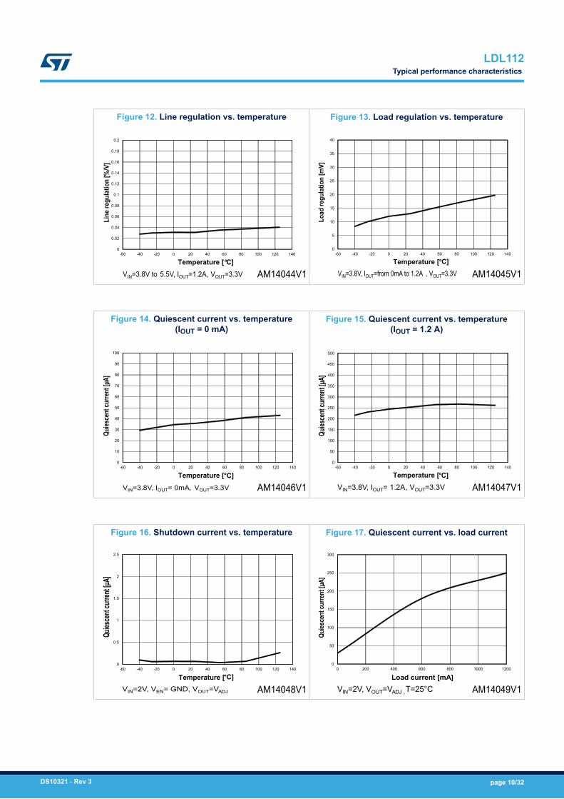
Figure 12. Line regulation vs. temperature
AM14044V1VIN=3.8V to 5.5V, IOUT=1.2A, VOUT=3.3V
0
0.02
0.04
0.06
0.08
0.1
0.12
0.14
0.16
0.18
0.2
-60 -40 -20 0 20 40 60 80 100 120 140
Line
regu
latio
n [%
/V]
Temperature [°C]
Figure 13. Load regulation vs. temperature
AM14045V1VIN=3.8V, IOUT=from 0mA to 1.2A , VOUT=3.3V
0
5
10
15
20
25
30
35
40
-60 -40 -20 0 20 40 60 80 100 120 140
Load
regu
latio
n [m
V]
Temperature [°C]
Figure 14. Quiescent current vs. temperature(IOUT = 0 mA)
AM14046V1VIN=3.8V, IOUT= 0mA, VOUT=3.3V
0
10
20
30
40
50
60
70
80
90
100
-60 -40 -20 0 20 40 60 80 100 120 140
Quies
cent
curre
nt [µ
A]
Temperature [°C]
Figure 15. Quiescent current vs. temperature(IOUT = 1.2 A)
AM14047V1VIN=3.8V, IOUT= 1.2A, VOUT=3.3V
0
50
100
150
200
250
300
350
400
450
500
-60 -40 -20 0 20 40 60 80 100 120 140
Quies
cent
curre
nt [µA
]
Temperature [°C]
Figure 16. Shutdown current vs. temperature
AM14048V1VIN=2V, VEN= GND, VOUT=VADJ
0
0.5
1
1.5
2
2.5
-60 -40 -20 0 20 40 60 80 100 120 140
Quies
cent
curre
nt [µA
]
Temperature [°C]
Figure 17. Quiescent current vs. load current
AM14049V1VIN=2V, VOUT=VADJ ,T=25°C
0
50
100
150
200
250
300
0 200 400 600 800 1000 1200
Quies
cent
curre
nt [µ
A]
Load current [mA]
LDL112Typical performance characteristics
DS10321 - Rev 3 page 10/32
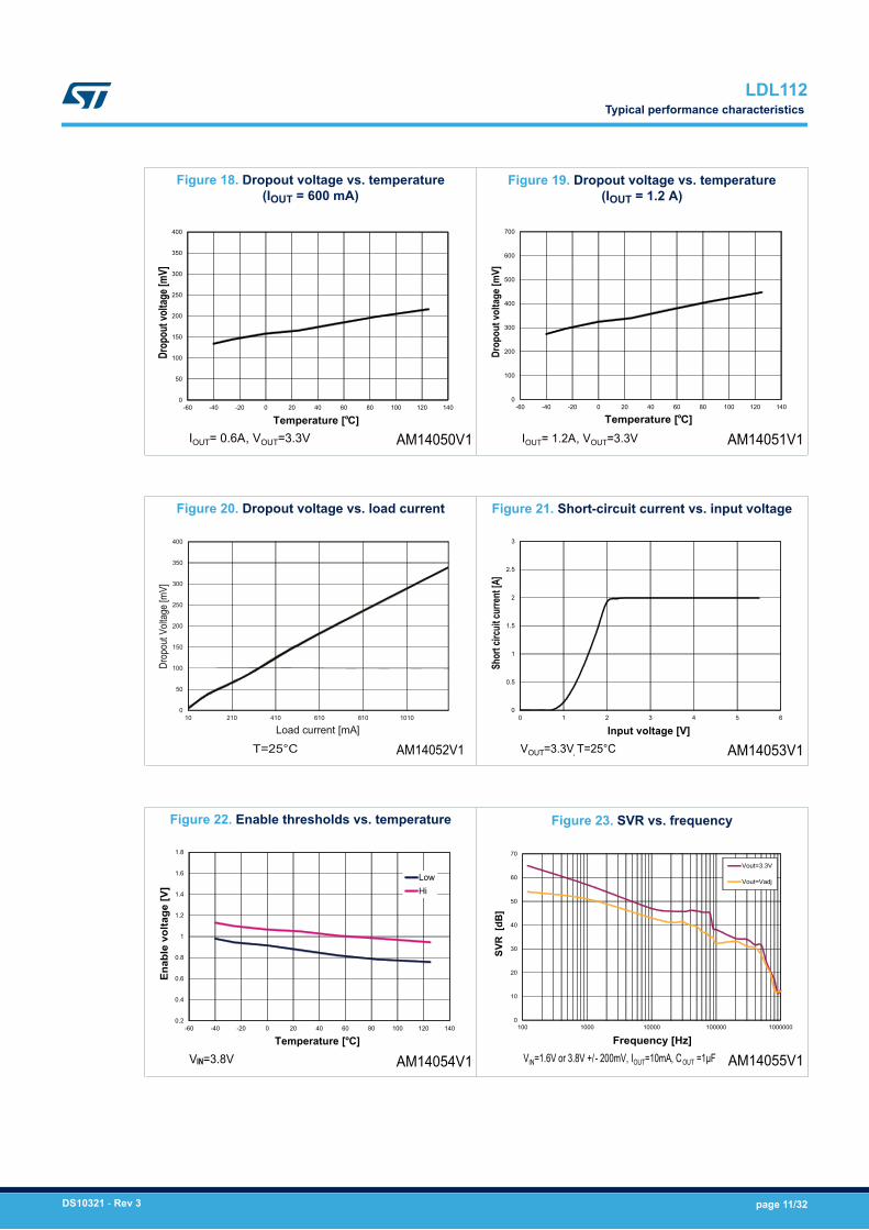
Figure 18. Dropout voltage vs. temperature(IOUT = 600 mA)
AM14050V1IOUT= 0.6A, VOUT=3.3V
0
50
100
150
200
250
300
350
400
-60 -40 -20 0 20 40 60 80 100 120 140
Drop
out v
oltag
e [mV
]
Temperature [°C]
Figure 19. Dropout voltage vs. temperature(IOUT = 1.2 A)
AM14051V1IOUT= 1.2A, VOUT=3.3V
0
100
200
300
400
500
600
700
-60 -40 -20 0 20 40 60 80 100 120 140
Drop
out v
olta
ge [m
V]
Temperature [°C]
Figure 20. Dropout voltage vs. load current
AM14052V1T=25°C
0
50
100
150
200
250
300
350
400
10 210 410 610 810 1010
Drop
out V
oltag
e [m
V]
Load current [mA]
Figure 21. Short-circuit current vs. input voltage
AM14053V1VOUT=3.3V, T=25°C
0
0.5
1
1.5
2
2.5
3
0 1 2 3 4 5 6
Shor
t circ
uit cu
rrent
[A]
Input voltage [V]
Figure 22. Enable thresholds vs. temperature
AM14054V1VIN=3.8V
0.2
0.4
0.6
0.8
1
1.2
1.4
1.6
1.8
-60 -40 -20 0 20 40 60 80 100 120 140
Enab
le v
olta
ge [V
]
Temperature [°C]
LowHi
Figure 23. SVR vs. frequency
AM14055V1
0
10
20
30
40
50
60
70
100 1000 10000 100000 1000000
SVR
[dB]
Frequency [Hz]
Vout=3.3V
Vout=Vadj
VIN=1.6V or 3.8V +/ - 200mV, IOUT=10mA, COUT =1µF
LDL112Typical performance characteristics
DS10321 - Rev 3 page 11/32
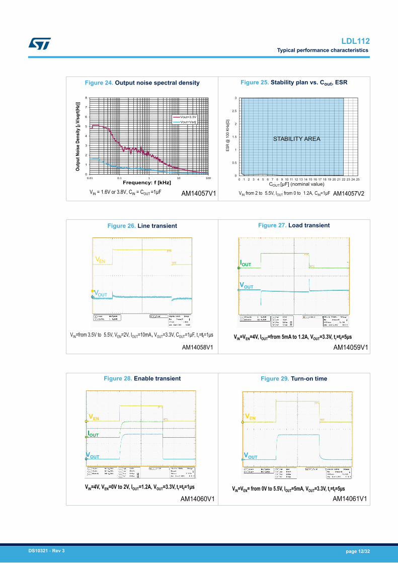
Figure 24. Output noise spectral density
AM14057V1VIN = 1.6V or 3.8V, CIN = COUT =1µF
0
1
2
3
4
5
6
7
8
0.01 0.1 1 10 100
Outp
ut N
oise
Den
sity
[mV/
sqrt(
Hz)]
Frequency: f [kHz]
Vout=3.3V
Vout=Vadj
Figure 25. Stability plan vs. Cout, ESR
AM14057V2
0
0.5
1
1.5
2
2.5
3
0 1 2 3 4 5 6 7 8 9 10 11 12 13 14 15 16 17 18 19 20 21 22 23 24 25
ESR
@ 1
00 K
Hz[Ω
]
COUT [µF] (nominal value)
VIN from 2 to 5.5V, IOUT from 0 to 1.2A, CIN=1µF
STABILITY AREA
Figure 26. Line transient
AM14058V1
VIN=from 3.5V to 5.5V, VEN=2V, IOUT=10mA, VOUT=3.3V, COUT=1µF, tr=tf=1µs
VOUT
VEN
Figure 27. Load transient
AM14059V1VIN=VEN=4V, IOUT=from 5mA to 1.2A, VOUT=3.3V, tr=tf=5µs
IOUT
VOUT
Figure 28. Enable transient
AM14060V1
VIN=4V, VEN=0V to 2V, IOUT=1.2A, VOUT=3.3V, tr=tf=1µs
IOUT
VOUT
VEN
Figure 29. Turn-on time
AM14061V1VIN=VEN= from 0V to 5.5V, IOUT=5mA, VOUT=3.3V, tr=tf=5µs
VOUT
VEN
LDL112Typical performance characteristics
DS10321 - Rev 3 page 12/32
8 Package mechanical data
In order to meet environmental requirements, ST offers these devices in different grades of ECOPACK®
packages, depending on their level of environmental compliance. ECOPACK® specifications, grade definitionsand product status are available at: www.st.com. ECOPACK® is an ST trademark.
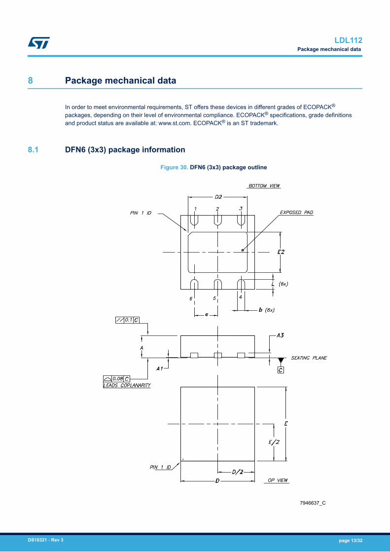
8.1 DFN6 (3x3) package information
Figure 30. DFN6 (3x3) package outline
7946637_C
LDL112Package mechanical data
DS10321 - Rev 3 page 13/32

Table 6. DFN6 (3x3) mechanical data
Dim.mm
Min. Typ. Max.
A 0.80 1
A1 0 0.02 0.05
A3 0.20
b 0.23 0.45
D 2.90 3 3.10
D2 2.23 2.50
E 2.90 3 3.10
E2 1.50 1.75
e 0.95
L 0.30 0.40 0.50
Figure 31. DFN6 (3x3) recommended footprint
7946637_C
LDL112DFN6 (3x3) package information
DS10321 - Rev 3 page 14/32

8.2 DFN6 (3x3) packing information
Figure 32. DFN6 (3x3) tape outline
7875978_N
LDL112DFN6 (3x3) packing information
DS10321 - Rev 3 page 15/32

Figure 33. DFN6 (3x3) reel outline
7875978_N
Table 7. DFN6 (3x3) tape and reel mechanical data
Dim.mm
Min. Typ. Max.
A0 3.20 3.30 3.40
B0 3.20 3.30 3.40
K0 1 1.10 1.20
LDL112DFN6 (3x3) packing information
DS10321 - Rev 3 page 16/32

8.3 DFN6 (2x2) package information
Figure 34. DFN6 (2x2) package outline
7733060
LDL112DFN6 (2x2) package information
DS10321 - Rev 3 page 17/32

Table 8. DFN6 (2x2) mechanical data
Dim.mm
Min. Typ. Max.
A 0.70 0.75 0.80
A1 0.00 0.02 0.05
A3 - 0.203 ref -
b 0.25 0.30 0.35
D - 2.00 -
E - 2.00 -
e - 0.50 -
D2 0.77 0.92 1.02
E2 1.30 1.45 1.55
K 0.15 - -
L 0.20 0.30 0.40
aaa - 0.05 -
bbb - 0.10 -
ccc - 0.10 -
ddd - 0.05 -
eee - 0.08 -
Figure 35. DFN6 (2x2) recommended footprint
7733060 revE
LDL112DFN6 (2x2) package information
DS10321 - Rev 3 page 18/32
8.4 DFN6 (2x2) packing information
Figure 36. DFN6 (2 x 2 mm) reel outline
Table 9. DFN6 (2 x 2 mm) tape and reel mechanical data
Dim.mm
Min. Typ. Max.
A 180
C 12.8 13.2
D 20.2
N 60
T 14.4
A0 2.4
B0 2.4
K0 1.3
P0 4
P 4
LDL112DFN6 (2x2) packing information
DS10321 - Rev 3 page 19/32

8.5 SO8 package information
Figure 37. SO-8 batwing package outline
0016023_G
Table 10. SO-8 batwing mechanical data
Dim.mm
Min. Typ. Max.
A 1.75
A1 0.10 0.25
A2 1.25
b 0.31 0.51
b1 0.28 0.48
c 0.10 0.25
c1 0.10 0.23
D 4.80 4.90 5.00
E 5.80 6.00 6.20
E1 3.80 3.90 4.00
e 1.27
h 0.25 0.50
L 0.40 1.27
L1 1.04
L2 0.25
k 0° 8°
ccc 0.10
LDL112SO8 package information
DS10321 - Rev 3 page 20/32
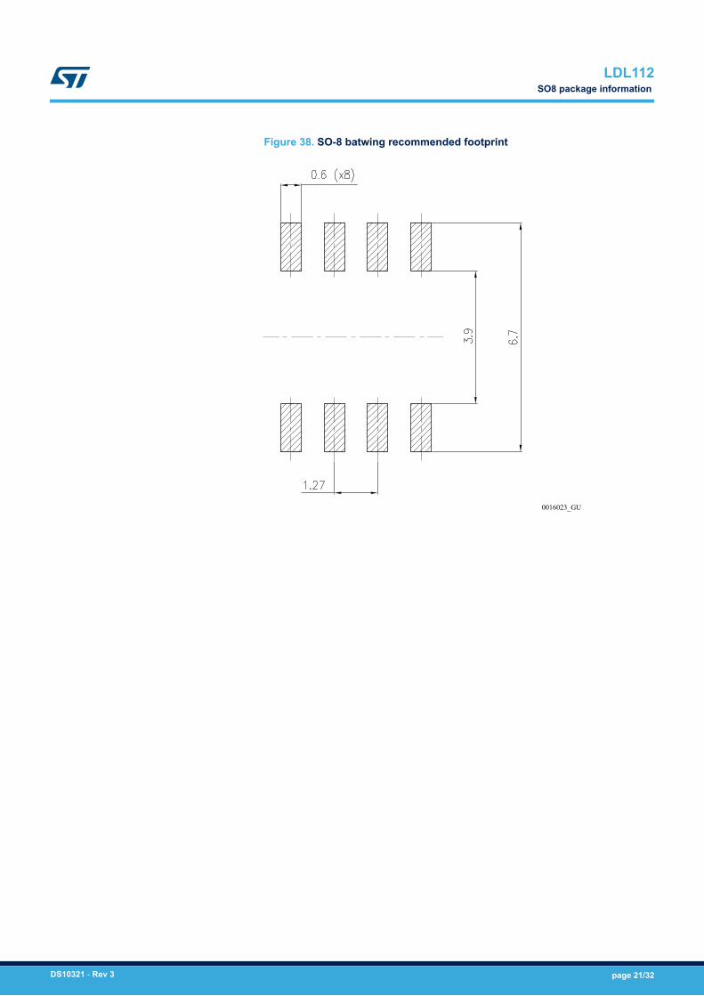
Figure 38. SO-8 batwing recommended footprint
0016023_GU
LDL112SO8 package information
DS10321 - Rev 3 page 21/32

8.6 SO8-batwing packing information
Figure 39. SO8-batwing tape and reel outline
Table 11. SO8-batwing mechanical data
Dim.mm
Min. Typ. Max.
A 330
C 12.8 13.2
D 20.2
N 60
T 22.4
A0 8.1 8.5
B0 5.5 5.9
K0 2.1 2.3
P0 3.9 4.1
P 7.9 8.1
LDL112SO8-batwing packing information
DS10321 - Rev 3 page 22/32
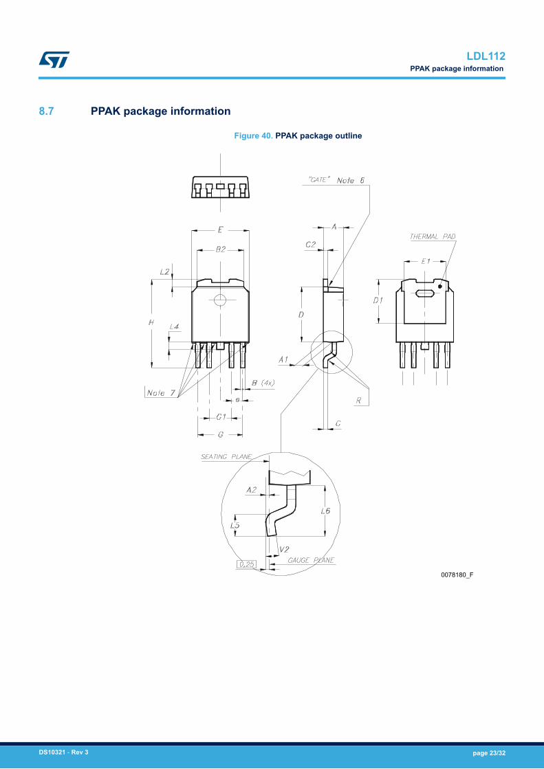
8.7 PPAK package information
Figure 40. PPAK package outline
0078180_F
LDL112PPAK package information
DS10321 - Rev 3 page 23/32

Table 12. PPAK mechanical data
Dim.mm
Min. Typ. Max.
A 2.2 2.4
A1 0.9 1.1
A2 0.03 0.23
B 0.4 0.6
B2 5.2 5.4
C 0.45 0.6
C2 0.48 0.6
D 6 6.2
D1 5.1
E 6.4 6.6
E1 4.7
e 1.27
G 4.9 5.25
G1 2.38 2.7
H 9.35 10.1
L2 0.8 1
L4 0.6 1
L5 1
L6 2.8
R 0.20
V2 0° 8°
LDL112PPAK package information
DS10321 - Rev 3 page 24/32

8.8 PPAK packing information
Figure 41. PPAK tape outline
P1A0 D1
P0
FW
E
D
B0K0
T
User direction of feed
P2
10 pitches cumul ativetolerance on tape +/- 0.2 mm
User direction of feed
R
Bending radius
B1
For machine ref. onlyincluding d raft andradii concentric around B0
AM08852v1
Top covertape
LDL112PPAK packing information
DS10321 - Rev 3 page 25/32

Figure 42. PPAK reel outline
Table 13. PPAK mechanical data
Tape Reel
Dim.mm
Dim.mm
Min. Max. Min. Max.
A0 6.8 7 A 330
B0 10.4 10.6 B 1.5
B1 12.1 C 12.8 13.2
D 1.5 1.6 D 20.2
D1 1.5 G 16.4 18.4
E 1.65 1.85 N 50
F 7.4 7.6 T 22.4
K0 2.55 2.75
P0 3.9 4.1 Base qty. 2500
P1 7.9 8.1 Base qty. 2500
P2 1.9 2.1
R 40
T 0.25 0.35
W 15.7 16.3
LDL112PPAK packing information
DS10321 - Rev 3 page 26/32
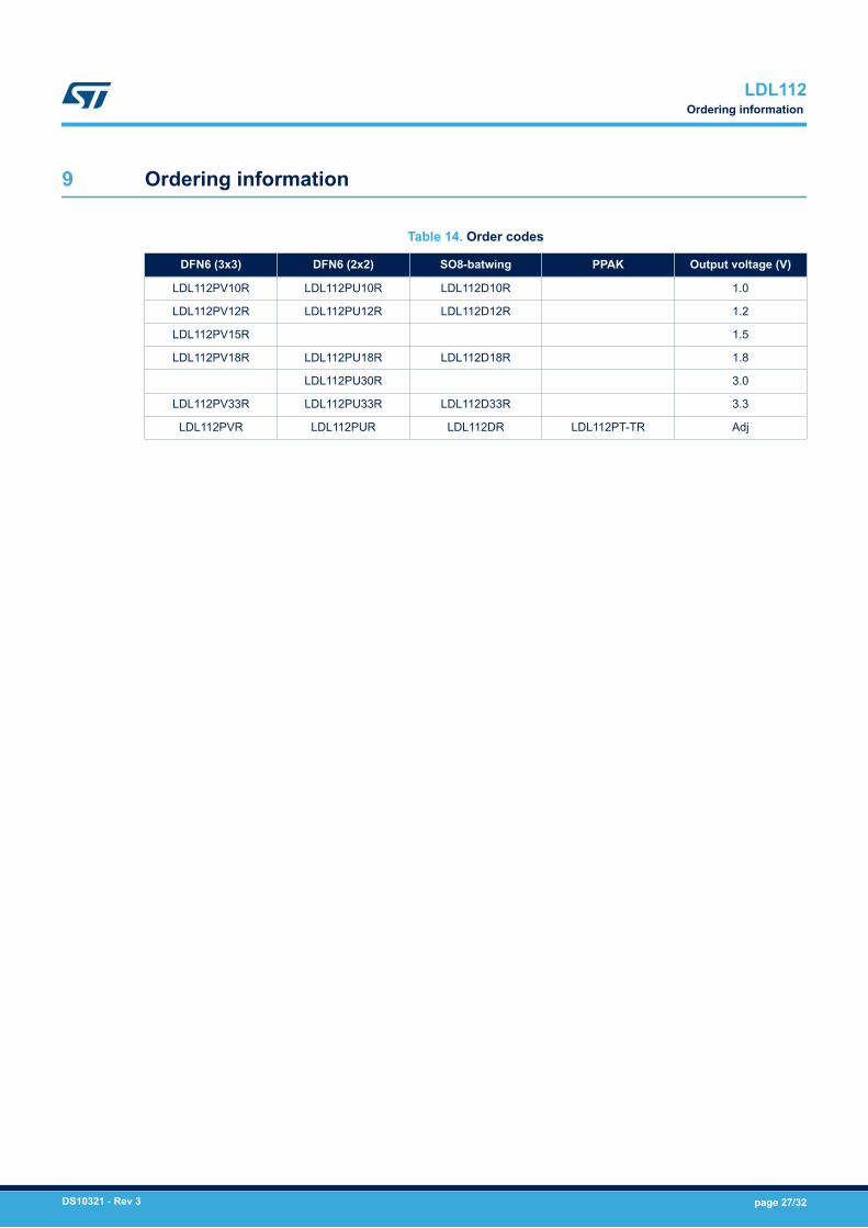
9 Ordering information
Table 14. Order codes
DFN6 (3x3) DFN6 (2x2) SO8-batwing PPAK Output voltage (V)
LDL112PV10R LDL112PU10R LDL112D10R 1.0
LDL112PV12R LDL112PU12R LDL112D12R 1.2
LDL112PV15R 1.5
LDL112PV18R LDL112PU18R LDL112D18R 1.8
LDL112PU30R 3.0
LDL112PV33R LDL112PU33R LDL112D33R 3.3
LDL112PVR LDL112PUR LDL112DR LDL112PT-TR Adj
LDL112Ordering information
DS10321 - Rev 3 page 27/32

Revision history
Table 15. Document revision history
Date Revision Changes
21-Nov-2014 1 Initial release.
28-Oct-2016 2Updated Figure 32. DFN6 (2x2) package outline. Modified Table 9. Ordercodes.
Minor text changes.
20-Feb-2019 3 Updated Table 14. Order codes.
LDL112
DS10321 - Rev 3 page 28/32

Contents
1 Diagram . . . . . . . . . . . . . . . . . . . . . . . . . . . . . . . . . . . . . . . . . . . . . . . . . . . . . . . . . . . . . . . . . . . . . . . . . . .2
2 Pin configuration . . . . . . . . . . . . . . . . . . . . . . . . . . . . . . . . . . . . . . . . . . . . . . . . . . . . . . . . . . . . . . . . . .3
3 Typical application. . . . . . . . . . . . . . . . . . . . . . . . . . . . . . . . . . . . . . . . . . . . . . . . . . . . . . . . . . . . . . . . .4
4 Maximum ratings . . . . . . . . . . . . . . . . . . . . . . . . . . . . . . . . . . . . . . . . . . . . . . . . . . . . . . . . . . . . . . . . . .5
5 Electrical characteristics. . . . . . . . . . . . . . . . . . . . . . . . . . . . . . . . . . . . . . . . . . . . . . . . . . . . . . . . . . .6
6 Application information. . . . . . . . . . . . . . . . . . . . . . . . . . . . . . . . . . . . . . . . . . . . . . . . . . . . . . . . . . . .8
6.1 Thermal and short-circuit protections . . . . . . . . . . . . . . . . . . . . . . . . . . . . . . . . . . . . . . . . . . . . . . 8
6.2 Output voltage setting for ADJ version . . . . . . . . . . . . . . . . . . . . . . . . . . . . . . . . . . . . . . . . . . . . . 8
6.3 Reverse current protection. . . . . . . . . . . . . . . . . . . . . . . . . . . . . . . . . . . . . . . . . . . . . . . . . . . . . . . 8
7 Typical performance characteristics . . . . . . . . . . . . . . . . . . . . . . . . . . . . . . . . . . . . . . . . . . . . . . .9
8 Package information. . . . . . . . . . . . . . . . . . . . . . . . . . . . . . . . . . . . . . . . . . . . . . . . . . . . . . . . . . . . . .13
8.1 DFN6 (3x3) package information . . . . . . . . . . . . . . . . . . . . . . . . . . . . . . . . . . . . . . . . . . . . . . . . 13
8.2 DFN6 (3x3) packing information . . . . . . . . . . . . . . . . . . . . . . . . . . . . . . . . . . . . . . . . . . . . . . . . . 14
8.3 DFN6 (2x2) package information . . . . . . . . . . . . . . . . . . . . . . . . . . . . . . . . . . . . . . . . . . . . . . . . 16
8.4 DFN6 (2x2) packing information . . . . . . . . . . . . . . . . . . . . . . . . . . . . . . . . . . . . . . . . . . . . . . . . . 18
8.5 SO8-batwing package information . . . . . . . . . . . . . . . . . . . . . . . . . . . . . . . . . . . . . . . . . . . . . . . 19
8.6 SO8-batwing packing information . . . . . . . . . . . . . . . . . . . . . . . . . . . . . . . . . . . . . . . . . . . . . . . . 21
8.7 PPAK package information . . . . . . . . . . . . . . . . . . . . . . . . . . . . . . . . . . . . . . . . . . . . . . . . . . . . . 22
8.8 PPAK packing information . . . . . . . . . . . . . . . . . . . . . . . . . . . . . . . . . . . . . . . . . . . . . . . . . . . . . . 24
9 Ordering information . . . . . . . . . . . . . . . . . . . . . . . . . . . . . . . . . . . . . . . . . . . . . . . . . . . . . . . . . . . . .27
Revision history . . . . . . . . . . . . . . . . . . . . . . . . . . . . . . . . . . . . . . . . . . . . . . . . . . . . . . . . . . . . . . . . . . . . . . .28
Contents . . . . . . . . . . . . . . . . . . . . . . . . . . . . . . . . . . . . . . . . . . . . . . . . . . . . . . . . . . . . . . . . . . . . . . . . . . . . . .29
List of tables . . . . . . . . . . . . . . . . . . . . . . . . . . . . . . . . . . . . . . . . . . . . . . . . . . . . . . . . . . . . . . . . . . . . . . . . . .30
List of figures. . . . . . . . . . . . . . . . . . . . . . . . . . . . . . . . . . . . . . . . . . . . . . . . . . . . . . . . . . . . . . . . . . . . . . . . . .31
LDL112Contents
DS10321 - Rev 3 page 29/32
List of tablesTable 1. Pin description. . . . . . . . . . . . . . . . . . . . . . . . . . . . . . . . . . . . . . . . . . . . . . . . . . . . . . . . . . . . . . . . . . . . . . 3Table 2. Absolute maximum ratings . . . . . . . . . . . . . . . . . . . . . . . . . . . . . . . . . . . . . . . . . . . . . . . . . . . . . . . . . . . . . 5Table 3. Thermal data. . . . . . . . . . . . . . . . . . . . . . . . . . . . . . . . . . . . . . . . . . . . . . . . . . . . . . . . . . . . . . . . . . . . . . . 5Table 4. LDL112 electrical characteristics (fixed version) . . . . . . . . . . . . . . . . . . . . . . . . . . . . . . . . . . . . . . . . . . . . . . . 6Table 5. LDL112 electrical characteristics (adjustable version) . . . . . . . . . . . . . . . . . . . . . . . . . . . . . . . . . . . . . . . . . . . 7Table 6. DFN6 (3x3) mechanical data . . . . . . . . . . . . . . . . . . . . . . . . . . . . . . . . . . . . . . . . . . . . . . . . . . . . . . . . . . . 14Table 7. DFN6 (3x3) tape and reel mechanical data . . . . . . . . . . . . . . . . . . . . . . . . . . . . . . . . . . . . . . . . . . . . . . . . . 16Table 8. DFN6 (2x2) mechanical data . . . . . . . . . . . . . . . . . . . . . . . . . . . . . . . . . . . . . . . . . . . . . . . . . . . . . . . . . . . 18Table 9. DFN6 (2 x 2 mm) tape and reel mechanical data . . . . . . . . . . . . . . . . . . . . . . . . . . . . . . . . . . . . . . . . . . . . . 19Table 10. SO-8 batwing mechanical data . . . . . . . . . . . . . . . . . . . . . . . . . . . . . . . . . . . . . . . . . . . . . . . . . . . . . . . . . 20Table 11. SO8-batwing mechanical data . . . . . . . . . . . . . . . . . . . . . . . . . . . . . . . . . . . . . . . . . . . . . . . . . . . . . . . . . . 22Table 12. PPAK mechanical data . . . . . . . . . . . . . . . . . . . . . . . . . . . . . . . . . . . . . . . . . . . . . . . . . . . . . . . . . . . . . . . 24Table 13. PPAK mechanical data . . . . . . . . . . . . . . . . . . . . . . . . . . . . . . . . . . . . . . . . . . . . . . . . . . . . . . . . . . . . . . . 26Table 14. Order codes . . . . . . . . . . . . . . . . . . . . . . . . . . . . . . . . . . . . . . . . . . . . . . . . . . . . . . . . . . . . . . . . . . . . . . 27Table 15. Document revision history . . . . . . . . . . . . . . . . . . . . . . . . . . . . . . . . . . . . . . . . . . . . . . . . . . . . . . . . . . . . . 28
LDL112List of tables
DS10321 - Rev 3 page 30/32

List of figuresFigure 2. Block diagram . . . . . . . . . . . . . . . . . . . . . . . . . . . . . . . . . . . . . . . . . . . . . . . . . . . . . . . . . . . . . . . . . . . . 2Figure 3. Pin connection DFN6 (3x3) and DFN6 (2x2) (top view) . . . . . . . . . . . . . . . . . . . . . . . . . . . . . . . . . . . . . . . . 3Figure 4. Pin connection PPAK and SO8 (top view) . . . . . . . . . . . . . . . . . . . . . . . . . . . . . . . . . . . . . . . . . . . . . . . . . 3Figure 5. Typical application circuits . . . . . . . . . . . . . . . . . . . . . . . . . . . . . . . . . . . . . . . . . . . . . . . . . . . . . . . . . . . . 4Figure 8. Output voltage vs. temperature (VOUT = 3.3 V, IOUT = 5 mA). . . . . . . . . . . . . . . . . . . . . . . . . . . . . . . . . . . . . 9Figure 9. Output voltage vs. temperature (VOUT = 3.3 V, IOUT = 1.2 A). . . . . . . . . . . . . . . . . . . . . . . . . . . . . . . . . . . . . 9Figure 10. Output voltage vs. temperature (VOUT = VADJ, IOUT = 5 mA). . . . . . . . . . . . . . . . . . . . . . . . . . . . . . . . . . . . . 9Figure 11. Output voltage vs. temperature (VOUT = VADJ, IOUT = 1.2 A) . . . . . . . . . . . . . . . . . . . . . . . . . . . . . . . . . . . . . 9Figure 12. Line regulation vs. temperature. . . . . . . . . . . . . . . . . . . . . . . . . . . . . . . . . . . . . . . . . . . . . . . . . . . . . . . . 10Figure 13. Load regulation vs. temperature . . . . . . . . . . . . . . . . . . . . . . . . . . . . . . . . . . . . . . . . . . . . . . . . . . . . . . . 10Figure 14. Quiescent current vs. temperature (IOUT = 0 mA) . . . . . . . . . . . . . . . . . . . . . . . . . . . . . . . . . . . . . . . . . . . 10Figure 15. Quiescent current vs. temperature (IOUT = 1.2 A) . . . . . . . . . . . . . . . . . . . . . . . . . . . . . . . . . . . . . . . . . . . 10Figure 16. Shutdown current vs. temperature. . . . . . . . . . . . . . . . . . . . . . . . . . . . . . . . . . . . . . . . . . . . . . . . . . . . . . 10Figure 17. Quiescent current vs. load current . . . . . . . . . . . . . . . . . . . . . . . . . . . . . . . . . . . . . . . . . . . . . . . . . . . . . . 10Figure 18. Dropout voltage vs. temperature (IOUT = 600 mA) . . . . . . . . . . . . . . . . . . . . . . . . . . . . . . . . . . . . . . . . . . . 11Figure 19. Dropout voltage vs. temperature (IOUT = 1.2 A) . . . . . . . . . . . . . . . . . . . . . . . . . . . . . . . . . . . . . . . . . . . . . 11Figure 20. Dropout voltage vs. load current . . . . . . . . . . . . . . . . . . . . . . . . . . . . . . . . . . . . . . . . . . . . . . . . . . . . . . . 11Figure 21. Short-circuit current vs. input voltage . . . . . . . . . . . . . . . . . . . . . . . . . . . . . . . . . . . . . . . . . . . . . . . . . . . . 11Figure 22. Enable thresholds vs. temperature . . . . . . . . . . . . . . . . . . . . . . . . . . . . . . . . . . . . . . . . . . . . . . . . . . . . . 11Figure 23. SVR vs. frequency . . . . . . . . . . . . . . . . . . . . . . . . . . . . . . . . . . . . . . . . . . . . . . . . . . . . . . . . . . . . . . . . 11Figure 24. Output noise spectral density . . . . . . . . . . . . . . . . . . . . . . . . . . . . . . . . . . . . . . . . . . . . . . . . . . . . . . . . . 12Figure 25. Stability plan vs. Cout, ESR. . . . . . . . . . . . . . . . . . . . . . . . . . . . . . . . . . . . . . . . . . . . . . . . . . . . . . . . . . . 12Figure 26. Line transient . . . . . . . . . . . . . . . . . . . . . . . . . . . . . . . . . . . . . . . . . . . . . . . . . . . . . . . . . . . . . . . . . . . . 12Figure 27. Load transient . . . . . . . . . . . . . . . . . . . . . . . . . . . . . . . . . . . . . . . . . . . . . . . . . . . . . . . . . . . . . . . . . . . 12Figure 28. Enable transient . . . . . . . . . . . . . . . . . . . . . . . . . . . . . . . . . . . . . . . . . . . . . . . . . . . . . . . . . . . . . . . . . . 12Figure 29. Turn-on time. . . . . . . . . . . . . . . . . . . . . . . . . . . . . . . . . . . . . . . . . . . . . . . . . . . . . . . . . . . . . . . . . . . . . 12Figure 30. DFN6 (3x3) package outline . . . . . . . . . . . . . . . . . . . . . . . . . . . . . . . . . . . . . . . . . . . . . . . . . . . . . . . . . . 13Figure 31. DFN6 (3x3) recommended footprint. . . . . . . . . . . . . . . . . . . . . . . . . . . . . . . . . . . . . . . . . . . . . . . . . . . . . 14Figure 32. DFN6 (3x3) tape outline. . . . . . . . . . . . . . . . . . . . . . . . . . . . . . . . . . . . . . . . . . . . . . . . . . . . . . . . . . . . . 15Figure 33. DFN6 (3x3) reel outline . . . . . . . . . . . . . . . . . . . . . . . . . . . . . . . . . . . . . . . . . . . . . . . . . . . . . . . . . . . . . 16Figure 34. DFN6 (2x2) package outline . . . . . . . . . . . . . . . . . . . . . . . . . . . . . . . . . . . . . . . . . . . . . . . . . . . . . . . . . . 17Figure 35. DFN6 (2x2) recommended footprint. . . . . . . . . . . . . . . . . . . . . . . . . . . . . . . . . . . . . . . . . . . . . . . . . . . . . 18Figure 36. DFN6 (2 x 2 mm) reel outline . . . . . . . . . . . . . . . . . . . . . . . . . . . . . . . . . . . . . . . . . . . . . . . . . . . . . . . . . 19Figure 37. SO-8 batwing package outline . . . . . . . . . . . . . . . . . . . . . . . . . . . . . . . . . . . . . . . . . . . . . . . . . . . . . . . . 20Figure 38. SO-8 batwing recommended footprint . . . . . . . . . . . . . . . . . . . . . . . . . . . . . . . . . . . . . . . . . . . . . . . . . . . 21Figure 39. SO8-batwing tape and reel outline . . . . . . . . . . . . . . . . . . . . . . . . . . . . . . . . . . . . . . . . . . . . . . . . . . . . . 22Figure 40. PPAK package outline . . . . . . . . . . . . . . . . . . . . . . . . . . . . . . . . . . . . . . . . . . . . . . . . . . . . . . . . . . . . . . 23Figure 41. PPAK tape outline . . . . . . . . . . . . . . . . . . . . . . . . . . . . . . . . . . . . . . . . . . . . . . . . . . . . . . . . . . . . . . . . . 25Figure 42. PPAK reel outline . . . . . . . . . . . . . . . . . . . . . . . . . . . . . . . . . . . . . . . . . . . . . . . . . . . . . . . . . . . . . . . . . 26
LDL112List of figures
DS10321 - Rev 3 page 31/32

IMPORTANT NOTICE – PLEASE READ CAREFULLY
STMicroelectronics NV and its subsidiaries (“ST”) reserve the right to make changes, corrections, enhancements, modifications, and improvements to STproducts and/or to this document at any time without notice. Purchasers should obtain the latest relevant information on ST products before placing orders. STproducts are sold pursuant to ST’s terms and conditions of sale in place at the time of order acknowledgement.
Purchasers are solely responsible for the choice, selection, and use of ST products and ST assumes no liability for application assistance or the design ofPurchasers’ products.
No license, express or implied, to any intellectual property right is granted by ST herein.
Resale of ST products with provisions different from the information set forth herein shall void any warranty granted by ST for such product.
ST and the ST logo are trademarks of ST. All other product or service names are the property of their respective owners.
Information in this document supersedes and replaces information previously supplied in any prior versions of this document.
© 2019 STMicroelectronics – All rights reserved
LDL112
DS10321 - Rev 3 page 32/32