datasheet rx 024 004 - silicon radar gmbh · 24-ghz highly integrated iq receiver rxˍ024ˍ004 data...
TRANSCRIPT

- 1 -
RXˍ024ˍ004 24-GHz Highly Integrated IQ Receiver in Silicon Germanium Technology
Data Sheet Status: Date: Author: Filename:
Final 2018-09-28 Silicon Radar GmbH DatasheetˍRXˍ024ˍ004ˍV2.1
Version: Product number: Package: Marking: Page:
2.1 RXˍ024ˍ004 QFN16, 3 × 3 mm² RX004 YYWW
1 of 12
Silicon Radar GmbH Im Technologiepark 1
15236 Frankfurt (Oder) Germany
fon +49.335.557 17 60 fax +49.335.557 10 50
https://www.siliconradar.com
24-GHz Highly Integrated IQ Receiver RXˍ024ˍ004 Data Sheet Version 2.1 2018-09-28
- 2 -
Version Control
Version Changed section Description of change Reason for change
1.0 All Data sheet revised Updates according to QMS rel. proc.
2.0 Specification Spec data revised Routinely revision
Packaging New package drawing Update
2.1 Pin Assignment pin-1 marking to package top view added Correction

24-GHz Highly Integrated IQ Receiver RXˍ024ˍ004 Data Sheet
Version 2.1 2018-09-28
- 3 -
Table of Contents
1 Features ................................................................................................................................ 4 1.1 Overview .................................................................................................................................................. 4 1.2 Applications .............................................................................................................................................. 4
2 Block Diagram ....................................................................................................................... 5
3 Pin Configuration .................................................................................................................. 5 3.1 Pin Assignment ......................................................................................................................................... 5 3.2 Pin Description ......................................................................................................................................... 6
4 Specification.......................................................................................................................... 6 4.1 Absolute Maximum Ratings ..................................................................................................................... 6 4.2 Operating Range ...................................................................................................................................... 7 4.3 Thermal Resistance .................................................................................................................................. 7 4.4 Electrical Characteristics .......................................................................................................................... 7
5 Packaging .............................................................................................................................. 8 5.1 Outline Dimensions .................................................................................................................................. 8 5.2 Package Code ........................................................................................................................................... 8 5.3 Qualification Test ..................................................................................................................................... 8
6 Application ............................................................................................................................ 9 6.1 Application Circuit Schematic .................................................................................................................. 9 6.2 Evaluation Board .................................................................................................................................... 10 6.3 Input / Output Stages ............................................................................................................................. 10
7 Measurement Results .......................................................................................................... 11
24-GHz Highly Integrated IQ Receiver RXˍ024ˍ004 Data Sheet
Version 2.1 2018-09-28
- 4 -
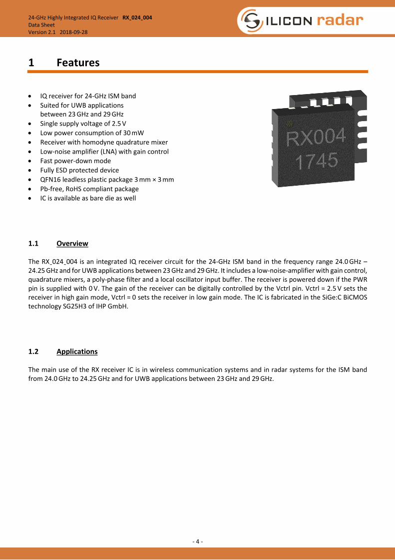
1 Features
IQ receiver for 24-GHz ISM band
Suited for UWB applications between 23 GHz and 29 GHz
Single supply voltage of 2.5 V
Low power consumption of 30 mW
Receiver with homodyne quadrature mixer
Low-noise amplifier (LNA) with gain control
Fast power-down mode
Fully ESD protected device
QFN16 leadless plastic package 3 mm × 3 mm
Pb-free, RoHS compliant package
IC is available as bare die as well
1.1 Overview The RXˍ024ˍ004 is an integrated IQ receiver circuit for the 24-GHz ISM band in the frequency range 24.0 GHz – 24.25 GHz and for UWB applications between 23 GHz and 29 GHz. It includes a low-noise-amplifier with gain control, quadrature mixers, a poly-phase filter and a local oscillator input buffer. The receiver is powered down if the PWR pin is supplied with 0 V. The gain of the receiver can be digitally controlled by the Vctrl pin. Vctrl = 2.5 V sets the receiver in high gain mode, Vctrl = 0 sets the receiver in low gain mode. The IC is fabricated in the SiGe:C BiCMOS technology SG25H3 of IHP GmbH.
1.2 Applications The main use of the RX receiver IC is in wireless communication systems and in radar systems for the ISM band from 24.0 GHz to 24.25 GHz and for UWB applications between 23 GHz and 29 GHz.
24-GHz Highly Integrated IQ Receiver RXˍ024ˍ004 Data Sheet
Version 2.1 2018-09-28
- 5 -
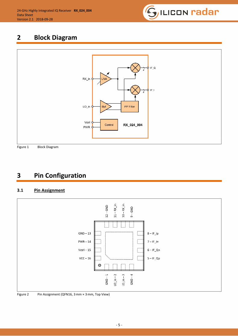
2 Block Diagram
Figure 1 Block Diagram
3 Pin Configuration
3.1 Pin Assignment
Figure 2 Pin Assignment (QFN16, 3 mm × 3 mm, Top View)

24-GHz Highly Integrated IQ Receiver RXˍ024ˍ004 Data Sheet
Version 2.1 2018-09-28
- 6 -
3.2 Pin Description Table 1 Pin Description
Pin Description
No. Name
1 GND Ground
2 LOˍin Local oscillator input, 50 Ω. Pin 2 and 3 have to be shorted on board close to the QFN package.
3 LOˍin
4 GND Ground
5 IFˍQp
IF outputs, DC coupled, external AC coupling capacitors required 6 IFˍQn
7 IFˍIn
8 IFˍlp
9 GND Ground
10 RXˍin Receiver input, 50 Ω. Pin 10 and 11 have to be shorted on board close to the QFN package.
11 RXˍin
12 GND Ground
13 GND
14 PWR Power-down input: low – power down, high – operate. CMOS logic input with 100-kΩ pull-up resistor.
15 Vctrl LNA gain control input: high – high gain, low – low gain. CMOS logic input with 100-kΩ pull-up resistor.
16 VCC Supply voltage, 2.5 V
(17) GND Exposed die attach pad of the QFN package, must be soldered to ground.
4 Specification
4.1 Absolute Maximum Ratings Attempted operation outside the absolute maximum ratings of the part may cause permanent damage to the part. Actual performance of the IC is only guaranteed within the operational specifications, not at absolute maximum ratings. Table 2 Absolute Maximum Ratings
Parameter Symbol Min Max Unit Condition / Remark
Supply Voltage VCC 2.7 V to GND
DC voltage at RF pins VDCRF 0 2 mV IC provides low ohmic circuit to GND for pin RXˍin and LOˍin
Junction temperature TJ 150 °C
Storage temperature range TSTG -65 150 °C
DC voltage at control inputs VCTL -0.3 VCC + 0.3 V Pin Vctrl and PWR
Input power into pin RXˍin, LOˍin PIN 0 dBm
ESD robustness VESD 500 V Class 1A 1)
1) According to ESDA / JEDEC Joint Standard for Electrostatic Discharge Sensitivity Testing, Human Body Model Component Level, ANSI / ESDA / JEDEC JS-001-2011

24-GHz Highly Integrated IQ Receiver RXˍ024ˍ004 Data Sheet
Version 2.1 2018-09-28
- 7 -
4.2 Operating Range Table 3 Operating Range
Parameter Symbol Min Max Unit Condition / Remark
Ambient temperature TA -40 85 °C
Supply voltage VCC 2.375 2.625 V (2.5 V ± 5%)
DC voltage at control inputs VCTL 0 VCC V Pin Vctrl and PWR
Note: Do not drive input signals without power supplied to the device.
4.3 Thermal Resistance Table 4 Thermal Resistance
Parameter Symbol Min Typ Max Unit Condition / Remark
Thermal resistance,
junction to ambient
Rthja
77 K / W JEDEC Standard JESD51-5
4.4 Electrical Characteristics TA = -40 °C to +85 °C unless otherwise noted. Typical values measured at TA = 25 °C and VCC = 2.5 V. Table 5 Electrical Characteristics
Parameter Symbol Min Typ Max Unit Condition / Remark
DC Parameters
Supply current consumption ICC 9 12.1 15 mA V(Vctrl) = V(PWR) = 2.5 V
RF Parameters
Receiver frequency range fRX 21.5 28.7 GHz
Receiver input impedance ZRXˍin 50 Ω
Input power into pin LOˍin PLOˍin -8 -5 -3 dBm
Number of LNA gain settings NG 2 Controlled by input Vctrl
Gain, high gain mode 14 16 17.5 dB V(Vctrl) = 2.5 V
Gain, low gain mode 4.9 7 9 dB V(Vctrl) = 0
IF frequency range fIF 0 200 MHz
IF output impedance 470 Ω Differential
IQ amplitude imbalance -1 1 dB
IQ phase imbalance -10 10 deg
Noise figure, high gain mode 4 dB Simulated
Noise figure, low gain mode 6 dB (double side band at fIF = 1 MHz)
Input compression point CPI -25 -15 dBm

24-GHz Highly Integrated IQ Receiver RXˍ024ˍ004 Data Sheet
Version 2.1 2018-09-28
- 8 -
5 Packaging
5.1 Outline Dimensions
Figure 3 Outline Dimensions of QFN16, 3 mm × 3 mm, 0.5 mm Pitch
5.2 Package Code Top-Side Markings RX004
YYWW
5.3 Qualification Test Table 6 Reliability and Environmental Test
Qualification Test JEDEC Standard Condition Pass / Fail
MSL3 J-STD-020E Reflow simulation 3 times at 260°C pass

24-GHz Highly Integrated IQ Receiver RXˍ024ˍ004 Data Sheet
Version 2.1 2018-09-28
- 9 -
Tp ≤ Tc = tp ≤
TS.min = TS.max =
tS = TL = tL =
t25°C-to-Tp ≤
260 °C 30 s 150 °C 200 °C 60 s – 120 s 217 °C 60 s – 150 s 480 s
Figure 4 Reflow Profile for Pb-Free Assembly according to JEDEC Standard J-STD-020E
6 Application
6.1 Application Circuit Schematic
Figure 5 Application Circuit

24-GHz Highly Integrated IQ Receiver RXˍ024ˍ004 Data Sheet
Version 2.1 2018-09-28
- 10 -
6.2 Evaluation Board
Figure 6 Evaluation Board Stack-up
Figure 7 Evaluation Board Layout Including Via Holes (40 mm × 50 mm, Top View)
6.3 Input / Output Stages The following figures show the simplified circuits of the input and output stages. It is important that the voltage applied to the input pins should never exceed VCC by more than 0.3 V. Otherwise, the supply current may be conducted through the upper ESD protection diode connected at the pin.
Figure 8 Equivalent I / O Circuits

24-GHz Highly Integrated IQ Receiver RXˍ024ˍ004 Data Sheet
Version 2.1 2018-09-28
- 11 -
7 Measurement Results
Figure 9 Conversion Gain, in Low-Gain and High-Gain Mode Figure 10 Conversion Gain vs. LO Power
Figure 11 Linearity, in Low-Gain and High-Gain Mode Figure 12 Conversion Gain for Various Temperatures
Figure 13 I-Q Phase Difference for Various Temperatures,
in High-Gain Mode
0
2
4
6
8
10
12
14
16
18
24 24.2 24.4 24.6 24.8 25
Co
nve
rsio
n G
ain
(d
B)
RF Frequency (GHz)
IF_I_HGIF_Q_HGIF_I_LGIF_Q_LG
0
2
4
6
8
10
12
14
16
18
20
-10 -8 -6 -4 -2 0 2
Co
nve
rsio
n G
ain
(d
B)
LO Power (dBm)
IF_I_HG
IF_Q_HG
IF_I_LG
IF_Q_LG
0
5
10
15
20
25
24.0 24.1 24.2 24.3 24.4 24.5
Co
nve
rsio
n G
ain
(d
B)
RF Frequency (GHz)
IF_I (-40°C) IF_Q (-40°C)
IF_I (-20°C) IF_Q (-20°C)
IF_I (0°C) IF_Q (0°C)
IF_I (25°C) IF_Q (25°C
IF_I (60°C) IF_Q (60°C)
IF_I (75°C) IF_Q (75°C)
70
75
80
85
90
95
100
24.0 24.1 24.2 24.3 24.4 24.5
Ph
ase
(d
egre
e)
RF Frequency (GHz)
-40°C -20°C0°C 25°C60°C 75°C
-30
-25
-20
-15
-10
-5
-30 -25 -20 -15 -10
Ou
tpu
t P
ow
er (
dB
m)
Input Power (dBm)
IF_I_HG
IF_Q_HG
IF_I_LG
IF_Q_LG
HG: 1dB ICP = -21dBm
LG: 1dB ICP = -14dBm

24-GHz Highly Integrated IQ Receiver RXˍ024ˍ004 Data Sheet
Version 2.1 2018-09-28
- 12 -
Disclaimer Silicon Radar GmbH 2018. The information contained herein is subject to change at any time without notice. Silicon Radar GmbH assumes no responsibility or liability for any loss, damage or defect of a product which is caused in whole or in part by
(i) use of any circuitry other than circuitry embodied in a Silicon Radar GmbH product, (ii) misuse or abuse including static discharge, neglect or accident, (iii) unauthorized modifications or repairs which have been soldered or altered during assembly and are not capable of being tested by Silicon
Radar GmbH under its normal test conditions, or (iv) improper installation, storage, handling, warehousing or transportation, or (v) being subjected to unusual physical, thermal, or electrical stress.
Disclaimer: Silicon Radar GmbH makes no warranty of any kind, express or implied, with regard to this material, and specifically disclaims any and all express or implied warranties, either in fact or by operation of law, statutory or otherwise, including the implied warranties of merchantability and fitness for use or a particular purpose, and any implied warranty arising from course of dealing or usage of trade, as well as any common-law duties relating to accuracy or lack of negligence, with respect to this material, any Silicon Radar product and any product documentation. Products sold by Silicon Radar are not suitable or intended to be used in a life support application or component, to operate nuclear facilities, or in other mission critical applications where human life may be involved or at stake. All sales are made conditioned upon compliance with the critical uses policy set forth below. CRITICAL USE EXCLUSION POLICY: BUYER AGREES NOT TO USE SILICON RADAR GMBH'S PRODUCTS FOR ANY APPLICATION OR IN ANY COMPONENTS USED IN LIFE SUPPORT DEVICES OR TO OPERATE NUCLEAR FACILITIES OR FOR USE IN OTHER MISSION-CRITICAL APPLICATIONS OR COMPONENTS WHERE HUMAN LIFE OR PROPERTY MAY BE AT STAKE. Silicon Radar GmbH owns all rights, title and interest to the intellectual property related to Silicon Radar GmbH's products, including any software, firmware, copyright, patent, or trademark. The sale of Silicon Radar GmbH products does not convey or imply any license under patent or other rights. Silicon Radar GmbH retains the copyright and trademark rights in all documents, catalogs and plans supplied pursuant to or ancillary to the sale of products or services by Silicon Radar GmbH. Unless otherwise agreed to in writing by Silicon Radar GmbH, any reproduction, modification, translation, compilation, or representation of this material shall be strictly prohibited.