is31lt3170/71 - issi integrated silicon solution, inc. – 2 rev. c, 10/20/2017 pin configuration...
TRANSCRIPT
IS31LT3170/71
Integrated Silicon Solution, Inc. – www.issi.com 1 Rev. D, 05/28/2018
10-TO-150MA CONSTANT-CURRENT LED DRIVER
June 2018
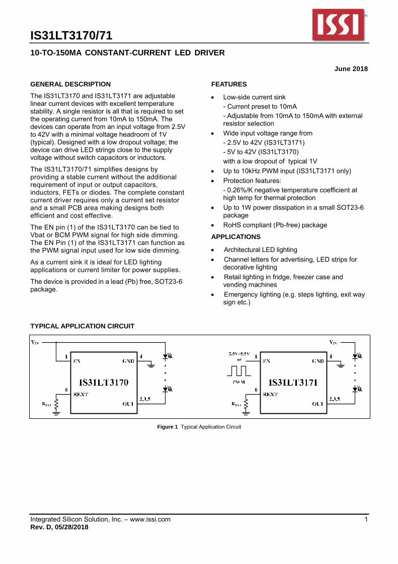
GENERAL DESCRIPTION
The IS31LT3170 and IS31LT3171 are adjustable linear current devices with excellent temperature stability. A single resistor is all that is required to set the operating current from 10mA to 150mA. The devices can operate from an input voltage from 2.5V to 42V with a minimal voltage headroom of 1V (typical). Designed with a low dropout voltage; the device can drive LED strings close to the supply voltage without switch capacitors or inductors.
The IS31LT3170/71 simplifies designs by providing a stable current without the additional requirement of input or output capacitors, inductors, FETs or diodes. The complete constant current driver requires only a current set resistor and a small PCB area making designs both efficient and cost effective.
The EN pin (1) of the IS31LT3170 can be tied to Vbat or BCM PWM signal for high side dimming. The EN Pin (1) of the IS31LT3171 can function as the PWM signal input used for low side dimming.
As a current sink it is ideal for LED lighting applications or current limiter for power supplies.
The device is provided in a lead (Pb) free, SOT23-6 package.
FEATURES
Low-side current sink - Current preset to 10mA - Adjustable from 10mA to 150mA with external resistor selection
Wide input voltage range from - 2.5V to 42V (IS31LT3171) - 5V to 42V (IS31LT3170) with a low dropout of typical 1V
Up to 10kHz PWM input (IS31LT3171 only)
Protection features: - 0.26%/K negative temperature coefficient at high temp for thermal protection
Up to 1W power dissipation in a small SOT23-6 package
RoHS compliant (Pb-free) package
APPLICATIONS
Architectural LED lighting
Channel letters for advertising, LED strips for decorative lighting
Retail lighting in fridge, freezer case and vending machines
Emergency lighting (e.g. steps lighting, exit way sign etc.)
TYPICAL APPLICATION CIRCUIT
Figure 1 Typical Application Circuit

IS31LT3170/71
Integrated Silicon Solution, Inc. – www.issi.com 2 Rev. D, 05/28/2018
PIN CONFIGURATION
Package Pin Configuration (Top View)
SOT23-6
PIN DESCRIPTION
No. Pin Description
1 EN Enable pin (PWM input IS31LT3171 only).
2,3,5 OUT Current sink.
4 GND Ground.
6 REXT Optional current adjust.

IS31LT3170/71
Integrated Silicon Solution, Inc. – www.issi.com 3 Rev. D, 05/28/2018
ORDERING INFORMATION Industrial Range: -40°C to +125°C
Order Part No. Package QTY/Reel
IS31LT3170-STLS4-TR IS31LT3171-STLS4-TR
SOT-23-6, Lead-free 3000
Copyright © 2018 Integrated Silicon Solution, Inc. All rights reserved. ISSI reserves the right to make changes to this specification and its products at any time without notice. ISSI assumes no liability arising out of the application or use of any information, products or services described herein. Customers are advised to obtain the latest version of this device specification before relying on any published information and before placing orders for products. Integrated Silicon Solution, Inc. does not recommend the use of any of its products in life support applications where the failure or malfunction of the product can reasonably be expected to cause failure of the life support system or to significantly affect its safety or effectiveness. Products are not authorized for use in such applications unless Integrated Silicon Solution, Inc. receives written assurance to its satisfaction, that: a.) the risk of injury or damage has been minimized; b.) the user assume all such risks; and c.) potential liability of Integrated Silicon Solution, Inc is adequately protected under the circumstances

IS31LT3170/71
Integrated Silicon Solution, Inc. – www.issi.com 4 Rev. D, 05/28/2018
ABSOLUTE MAXIMUM RATINGS (Note 1) Maximum enable voltage, VEN(MAX) only for IS31LT3170-STLS4-TR VEN(MAX) only for IS31LT3171-STLS4-TR
45V 6V
Maximum output current, IOUT(MAX) 200mA Maximum output voltage, VOUT(MAX) 45V Reverse voltage between all terminals, VR 0.5V Package thermal resistance, junction to ambient (4 layer standard test PCB based on JEDEC standard), θJA
130°C/W
Power dissipation, PD(MAX) (Note 2) 0.77W Maximum junction temperature, TJMAX +150°C Storage temperature range, TSTG -65°C ~ +150°C Operating temperature range, TA=TJ -40°C ~ +125°C ESD (HBM) ESD (CDM)
±2kV ±500V
Note 1: Stresses beyond those listed under “Absolute Maximum Ratings” may cause permanent damage to the device. These are stress ratings only and functional operation of the device at these or any other condition beyond those indicated in the operational sections of the specifications is not implied. Exposure to absolute maximum rating conditions for extended periods may affect device reliability. Note 2: Detail information please refer to package thermal de-rating curve on Page 14. ELECTRICAL CHARACTERISTICS “” This symbol in the table means these parameters are for IS31LT3170-STLS4-TR. “” This symbol in the table means these parameters are for IS31LT3171-STLS4-TR. Test condition is TA = TJ = 25°C, unless otherwise specified. (Note 3)
Symbol Parameter Condition Min. Typ. Max. Unit
VBD_OUT OUT pin breakdown voltage VEN= 0V 42 V
IEN Enable current VEN= 24V 0.35
mA VEN= 3.3V 0.35
RINT Internal resistor IRINT = 10mA 106 Ω
IOUT
Output current
VOUT = 1.4V, VEN = 24V, REXT OPEN
9 10 11
mA VOUT = 1.4V, VEN = 3.3V, REXT OPEN
9 10 11
VOUT > 2.0V, VEN = 24V, REXT = 10Ω
98 113 123
mA VOUT > 2.0V, VEN = 3.3V, REXT = 10Ω
98 113 123
Output current Range (Note 4, 5)
VOUT > 2.0V, VEN = 24V 10 150
mA
VOUT > 2.0V, VEN = 3.3V 10 150

IS31LT3170/71
Integrated Silicon Solution, Inc. – www.issi.com 5 Rev. D, 05/28/2018
DC CHARACTERISTICS WITH STABILIZED LED LOAD “” This symbol in the table means these parameters are for IS31LT3170-STLS4-TR. “” This symbol in the table means these parameters are for IS31LT3171-STLS4-TR. Test condition is TA= TJ= 25°C, unless otherwise specified. (Note 3)
Symbol Parameter Condition Min. Typ. Max. Unit
VS Sufficient supply voltage on EN pin
5 42
V 2.5 5.5
VHR Lowest sufficient headroom voltage on OUT pin
IOUT = 100mA 1 1.2 V
∆IOUT/IOUT
(Note 4)
Output current change versus ambient temp change
VOUT > 2.0V, VEN = 24V, REXT = 10Ω
-0.26 %/K
VOUT > 2.0V, VEN = 3.3V, REXT = 10Ω
-0.26
Output current change versus Vout
VOUT > 2.0V, VEN = 24V, REXT = 10Ω
1.9 %/V
VOUT > 2.0V, VEN = 3.3V, REXT = 10Ω
1.9
Note 3: Production testing of the device is performed at 25°C. Functional operation of the device and parameters specified over -40°C to +125°C temperature range, are guaranteed by design and characterization.
Note 4: Guaranteed by design.
Note 5: The maximum output current is dependent on the PCB board design, air flow, ambient temperature and power dissipation in the device. Please refer to the package thermal de-rating curve on Page 14 for more detail information.

IS31LT3170/71
Integrated Silicon Solution, Inc. – www.issi.com 6 Rev. D, 05/28/2018
FUNCTIONAL BLOCK DIAGRAM
IS31LT3170
IS31LT3171

IS31LT3170/71
Integrated Silicon Solution, Inc. – www.issi.com 7 Rev. D, 05/28/2018
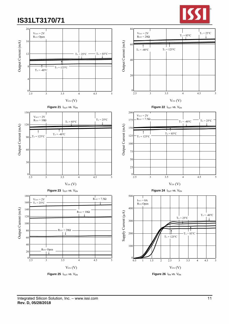
TYPICAL PERFORMANCE CHARACTERISTICS
IS31LT3170
Output Voltage (V)
Out
put C
urre
nt (
mA
)
0
5
10
15
20
25
30
0.5 2 3.5 5 6.5 8 9.5 11 12.5 14
VEN = 42VREXT Open
TA = -40°C
TA = 85°C
TA = 125°C
TA = 25°C
Figure 2 IOUT vs. VOUT
Output Voltage (V)
Out
put C
urre
nt (
mA
)
0.5 2 3.5 5 6.5 8 9.5 11 12.5 140
50
100
150
VEN = 42VREXT = 10Ω
TA = 125°C
TA = 85°C
TA = 25°CTA = -40°C
Figure 4 IOUT vs. VOUT
Output Voltage (V)
Out
put C
urre
nt (
mA
)
0
20
40
60
80
100
120
140
160
180
200
0 2 4 6 8 10 12 14
VEN = 5VfPWM = 100Hz@1% Duty CycleTA = 25°C
REXT = 7.5Ω
REXT = 10Ω
REXT= 20Ω
REXT Open
Figure 6 IOUT vs. VOUT
Output Voltage (V)O
utpu
t Cur
rent
(m
A)
0.5 2 3.5 5 6.5 8 9.5 11 12.5 140
20
40
60
80
VEN = 42VREXT = 20Ω
TA = 125°CTA = 85°C
TA = 25°C TA = -40°C
Figure 3 IOUT vs. VOUT
Output Voltage (V)
Out
put C
urre
nt (
mA
)
0.5 2 3.5 5 6.5 8 9.5 11 12.5 140
20
40
60
80
100
120
140
160
180VEN = 42VREXT = 7.5Ω
TA = 125°C
TA = 85°C
TA = 25°CTA = -40°C
Figure 5 IOUT vs. VOUT
Output Voltage (V)
Out
put C
urre
nt (
mA
)
0
20
40
60
80
100
120
140
160
180
200
0 2 4 6 8 10 12 14
VEN = 42VTA = 25°C
REXT Open
REXT = 20Ω
REXT = 10ΩREXT = 7.5Ω
Figure 7 IOUT vs. VOUT

IS31LT3170/71
Integrated Silicon Solution, Inc. – www.issi.com 8 Rev. D, 05/28/2018
VEN (V)
Out
put C
urre
nt (
mA
)
0
4
8
12
16
20
5 15 25 35 42
VOUT = 2VREXT Open
TA = -40°C TA = 125°C
TA = 85°CTA = 25°C
Figure 8 IOUT vs. VEN
VEN (V)
Out
put C
urre
nt (
mA
)
5 15 25 35 420
30
60
90
120
150
VOUT = 2VREXT = 10Ω
TA = 125°CTA = -40°C
TA = 25°CTA = 85°C
Figure 10 IOUT vs. VEN
VEN (V)
Out
put C
urre
nt (
mA
)
420
20
40
60
80
100
120
140
160
180
0 5 10 15 20 25 30 35 40
VOUT = 2VTA = 25°C
REXT = 7.5Ω
REXT = 10Ω
REXT = 20Ω
REXT Open
Figure 12 IOUT vs. VEN
VEN (V)
Out
put C
urre
nt (
mA
)
5 15 25 35 42
TA = 125°C
0
20
40
60
80
VOUT = 2VREXT = 20Ω
TA = -40°C
TA = 25°CTA = 85°C
Figure 9 IOUT vs. VEN
VEN (V)
Out
put C
urre
nt (
mA
)
5 15 25 35 420
25
50
75
100
125
150
175
200
VOUT = 2VREXT = 7.5Ω
TA = 125°CTA = -40°C
TA = 25°CTA = 85°C
Figure 11 IOUT vs. VEN
VEN (V)
Sup
ply
Cur
rent
(µ
A)
420 5 10 15 20 25 30 35 400
100
200
300
400
500
IOUT = 0AREXT Open
TA = 125°C
TA = 85°C
TA = 25°C
TA = -40°C
Figure 13 IEN vs. VEN

IS31LT3170/71
Integrated Silicon Solution, Inc. – www.issi.com 9 Rev. D, 05/28/2018
REXT (Ω)
Out
put C
urre
nt (
mA
)
0
50
100
150
200
250
1 10 100
VEN = 42VVOUT = 2V
Figure 14 IOUT vs. REXT

IS31LT3170/71
Integrated Silicon Solution, Inc. – www.issi.com 10 Rev. D, 05/28/2018
IS31LT3171
Output Voltage (V)
Out
put C
urre
nt (
mA
)
0
5
10
15
20
25
30
0.5 2 3.5 5 6.5 8 9.5 11 12.5 14
VEN = 3.3VREXT Open
TA = -40°C
TA = 125°C
TA = 25°CTA = 85°C
Figure 15 IOUT vs. VOUT
Output Voltage (V)
Out
put C
urre
nt (
mA
)
0.5 2 3.5 5 6.5 8 9.5 11 12.5 140
50
100
150
VEN = 3.3VREXT = 10Ω
TA = 125°C
TA = 85°C
TA = 25°CTA = -40°C
Figure 17 IOUT vs. VOUT
Output Voltage (V)
Out
put C
urre
nt (
mA
)
0
20
40
60
80
100
120
140
160
180
200
0 2 4 6 8 10 12 14
VEN = 5VfPWM = 100Hz@1% Duty CycleTA = 25°C
REXT = 7.5Ω
REXT = 10Ω
REXT= 20Ω
REXT Open
Figure 19 IOUT vs. VOUT
Output Voltage (V)
Out
put C
urre
nt (
mA
)
0.5 2 3.5 5 6.5 8 9.5 11 12.5 140
20
40
60
80
VEN = 3.3VREXT = 20Ω
TA = 125°C
TA = 85°C
TA = -40°CTA = 25°C
Figure 16 IOUT vs. VOUT
Output Voltage (V)
Out
put C
urre
nt (
mA
)
0.5 2 3.5 5 6.5 8 9.5 11 12.5 140
20
40
60
80
100
120
140
160
180VEN = 3.3VREXT = 7.5Ω
TA = -40°CTA = 25°C
TA = 125°C
TA = 85°C
Figure 18 IOUT vs. VOUT
Output Voltage (V)
Out
put C
urre
nt (
mA
)
0
20
40
60
80
100
120
140
160
180
200
0 2 4 6 8 10 12 14
VEN = 3.3VTA = 25°C
REXT = 7.5Ω
REXT = 10Ω
REXT = 20Ω
REXT Open
Figure 20 IOUT vs. VOUT
IS31LT3170/71
Integrated Silicon Solution, Inc. – www.issi.com 11 Rev. D, 05/28/2018
VEN (V)
Out
put C
urre
nt (
mA
)
0
4
8
12
16
20
2.5 3 3.5 4 4.5 5
VOUT = 2VREXT Open
TA = -40°CTA = 125°C
TA = 85°CTA = 25°C
Figure 21 IOUT vs. VEN
VEN (V)
Out
put C
urre
nt (
mA
)
0
30
60
90
120
150
VOUT = 2VREXT = 10Ω
TA = 125°CTA = -40°C
TA = 25°CTA = 85°C
2.5 3 3.5 4 4.5 5
Figure 23 IOUT vs. VEN
VEN (V)
Out
put C
urre
nt (
mA
)
0
20
40
60
80
100
120
140
160
180
2.5 3 3.5 4 4.5 5
REXT = 7.5Ω
REXT = 10Ω
REXT = 20Ω
REXT Open
VOUT = 2VTA = 25°C
Figure 25 IOUT vs. VEN
VEN (V)
Out
put C
urre
nt (
mA
)
0
20
40
60
80
2.5 3 3.5 4 4.5 5
VOUT = 2VREXT = 20Ω
TA = -40°C TA = 125°C
TA = 25°CTA = 85°C
Figure 22 IOUT vs. VEN
VEN (V)
Out
put C
urre
nt (
mA
)
0
25
50
75
100
125
150
175
200VOUT = 2VREXT = 7.5Ω
2.5 3 3.5 4 4.5 5
TA = 125°CTA = 85°C
TA = 25°CTA = -40°C
Figure 24 IOUT vs. VEN
VEN (V)
Sup
ply
Cur
rent
(µ
A)
0
100
200
300
400
500
0.5 1 1.5 2 2.5 3 3.5 4 4.5 5
IOUT = 0AREXT Open
TA = 125°CTA = 85°C
TA = -40°CTA = 25°C
Figure 26 IEN vs. VEN

IS31LT3170/71
Integrated Silicon Solution, Inc. – www.issi.com 12 Rev. D, 05/28/2018
REXT (Ω)
Out
put C
urre
nt (
mA
)
0
50
100
150
200
250
1 10 100
VEN = 3.3VVOUT = 2V
Figure 27 IOUT vs. REXT
Time (200ns/Div)
IOUT
50mA/Div
VEN
2V/Div
VOUT = 3V, 3 LEDsVEN = 5V, 100Hz, 50% Duty CycleREXT = 10ΩTJ = 25°C
Figure 29 VEN vs. IOUT Delay and Rising Edge
Time (100ns/Div)
IOUT
50mA/Div
VEN
2V/Div
VOUT = 3V, 3 LEDsVEN = 5V, 100Hz, 50% Duty CycleREXT = 10ΩTJ = -40°C
Figure 31 VEN vs. IOUT Delay and Falling Edge
Time (200ns/Div)
IOUT
50mA/Div
VEN
2V/Div
VOUT = 3V, 3 LEDsVEN = 5V, 100Hz, 50% Duty CycleREXT = 10ΩTJ = -40°C
Figure 28 VEN vs. IOUT Delay and Rising Edge
Time (200ns/Div)
IOUT
50mA/Div
VEN
2V/Div
VOUT = 3V, 3 LEDsVEN = 5V, 100Hz, 50% Duty CycleREXT = 10ΩTJ = 125°C
Figure 30 VEN vs. IOUT Delay and Rising Edge
Time (100ns/Div)
IOUT
50mA/Div
VEN
2V/Div
VOUT = 3V, 3 LEDsVEN = 5V, 100Hz, 50% Duty CycleREXT = 10ΩTJ = 25°C
Figure 32 VEN vs. IOUT Delay and Falling Edge

IS31LT3170/71
Integrated Silicon Solution, Inc. – www.issi.com 13 Rev. D, 05/28/2018
Time (100ns/Div)
IOUT
50mA/Div
VEN
2V/Div
VOUT = 3V, 3 LEDsVEN = 5V, 100Hz, 50% Duty CycleREXT = 10ΩTJ = 125°C
Figure 33 VEN vs. IOUT Delay and Falling Edge

IS31LT3170/71
Integrated Silicon Solution, Inc. – www.issi.com 14 Rev. D, 05/28/2018
APPLICATIONS INFORMATION IS31LT3170/71 provides an easy constant current source solution for LED lighting applications. It uses an external resistor to adjust the LED current from 10mA to 150mA. The LED current can be determined by the Equation (1):
EXT
EXTINTSET R
RRmAI
10 (1)
Where RINT (106Ω Typ.) is an internal resistor and REXT is the external resistor.
Paralleling a low tolerance resistor REXT with the internal resistor RINT will improve the overall accuracy of the current sense resistance. The resulting output current will vary slightly lower due to the negative temperature coefficient (NTC) resulting from the self heating of the IS31LT3170/71.
HIGH INPUT VOLTAGE APPLICATION
When driving a long string of LEDs whose total forward voltage drop exceeds the IS31LT3170 VBD_OUT limit of 42V, it is possible to stack several LEDs(such as 2 LEDs) between the EN pin and the OUT pins 2,3, and 5 so the voltage on the EN pin is higher than 5V. The remaining string of LEDs can then be placed between power supply +VS and EN pin, (Figure 34). The number of LEDs required to stack at EN pin will depend on the LED’s forward voltage drop (VF) and the +VS value.
Figure 34 High Input Voltage Application Circuit
Note: when operating the IS31LT3170 at voltages exceeding the device operating limits, care needs to be taken to keep the EN pin and OUT pin voltage below 42V.
THERMAL PROTECTION AND DISSIPATION
The IS31LT3170/71 implements thermal foldback protection to reduce the LED current when the package’s thermal dissipation is exceeded and prevent “thermal runaway”. The thermal foldback implements a negative temperature coefficient (NTC) of -0.26%/K.
When operating the chip at high ambient temperatures, or when driving maximum load current, care must be taken to avoid exceeding the package power dissipation limits. Exceeding the package dissipation will cause the device to enter thermal protection mode. The maximum package power dissipation can be calculated using the following Equation (2):
JA
AMAXJMAXD
TTP
)()( (2)
Where TJ(MAX) is the maximum junction temperature, TA is the ambient temperature, and θJA is the junction to ambient thermal resistance; a metric for the relative thermal performance of a package.
The recommended maximum operating junction temperature, TJ(MAX), is 125°C and so the maximum ambient temperature is determined by the package parameter; θJA. The θJA for the IS31LT3170/71 SOT23-6 package, is 130°C/W.
Therefore the maximum power dissipation at TA = 25°C is:
WWC
CCP MAXD 77.0
/130
25125)(
The actual power dissipation PD is:
ENENOUTOUTD IVIVP (3)
To ensure the performance, the die temperature (TJ) of the IS31LT3170/71 should not exceed 125°C. The graph below gives details for the package power derating.
0
0.2
0.4
0.6
0.8
1
Temperature (°C)
Pow
er D
issi
patio
n (W
)
-40 -25 -10 5 20 35 50 65 80 95 110 125
SOT23-6
Figure 35 PD vs. TA

IS31LT3170/71
Integrated Silicon Solution, Inc. – www.issi.com 15 Rev. D, 05/28/2018
The thermal resistance is achieved by mounting the IS31LT3170/71 on a standard FR4 double-sided printed circuit board (PCB) with a copper area of a few square inches on each side of the board under the IS31LT3170/71. Multiple thermal vias, as shown in Figure 36, help to conduct the heat from the exposed pad of the IS31LT3170/71 to the copper on each side of the board. The thermal resistance can be reduced by using a metal substrate or by adding a heatsink.
Figure 36 Board Via Layout For Thermal Dissipation

IS31LT3170/71
Integrated Silicon Solution, Inc. – www.issi.com 16 Rev. D, 05/28/2018
CLASSIFICATION REFLOW PROFILES
Profile Feature Pb-Free Assembly
Preheat & Soak
Temperature min (Tsmin)
Temperature max (Tsmax)
Time (Tsmin to Tsmax) (ts)
150°C
200°C
60-120 seconds
Average ramp-up rate (Tsmax to Tp) 3°C/second max.
Liquidous temperature (TL)
Time at liquidous (tL)
217°C
60-150 seconds
Peak package body temperature (Tp)* Max 260°C
Time (tp)** within 5°C of the specified
classification temperature (Tc) Max 30 seconds
Average ramp-down rate (Tp to Tsmax) 6°C/second max.
Time 25°C to peak temperature 8 minutes max.
Figure 37 Classification Profile

IS31LT3170/71
Integrated Silicon Solution, Inc. – www.issi.com 17 Rev. D, 05/28/2018
PACKAGE INFORMATION SOT23-6

IS31LT3170/71
Integrated Silicon Solution, Inc. – www.issi.com 18 Rev. D, 05/28/2018
RECOMMENDED LAND PATTERN SOT23-6
Note: 1. Land pattern complies to IPC-7351. 2. All dimensions in MM. 3. This document (including dimensions, notes & specs) is a recommendation based on typical circuit board manufacturing parameters. Since land pattern design depends on many factors unknown (eg. User’s board manufacturing specs), user must determine suitability for use.
IS31LT3170/71
Integrated Silicon Solution, Inc. – www.issi.com 19 Rev. D, 05/28/2018
REVISION HISTORY
Revision Detail Information Date
A Initial release 2016.05.04
B Update EC table (output current limit) 2016.07.05
C Update θJA value 2017.10.20
D Update IOUT in EC table 2018.05.28