1.1 overview - global home | industrial devices & … pin the specifications of pins in this lsi...
TRANSCRIPT

1.1 OverviewThe MN103S is a 32-bit micro controller combining ease of use intended for programs development in the C languagewith a simple, high-performance architecture made possible through pursuit of cost performance.Built around a compact 32-bit CPU with a basic instruction word length of 1 byte, this LSI includes internal memory forinstructions and data, a clock generator, bus controller, interrupt controller, watchdog timer, standard peripheral circuitrysuch as timers and serial interfaces, PWM circuit best suited to controlling 3- phase motors, arithmetic unit for speed-upof inverter control and analog circuits. (A/D converters and VGA (Variable Gain Amplifier)) for motor position control.The MN103S Series high-speed CPU coupled with abundance of peripheral features provides an easy means of devel-oping on LSI for motor and power control applications requiring fast response a feature previously unavailable withconventional micro controllers.
MN103SFX1K/X2K/X3K/X5K/X6K/X7K32-bit Single-chip Microcontroller
PubNo. 232X701-015E
Publication date: April 2018 1

1.2 Product SummaryThis manual describes LSI in the following Table 1.2-1 .
Table 1.2-1 Product Summary
LSI ROM size RAM size Classification Package
MN103SFX7K / X3K 256 KB 12 KB Flash EEPROM ver-sion
LQFP 100 pinQFP 100 pin
MN103SFX6K / X2K 256 KB 12 KB Flash EEPROM ver-sion
TQFP 80 pinLQFP 80 pin
MN103SFX5K / X1K 256 KB 12 KB Flash EEPROM ver-sion
TQFP 64 pin
This LSI's functions are listed in Table 1.2-2 .
Table 1.2-2 Functions listFunction MN103S
FX7KMN103SFX6K
MN103SFX5K
MN103SFX3K
MN103SFX2K
MN103SFX1K
Number of pins 100 80 64 100 80 64
General purpose ports I/O port 74 54 42 82 62 50
Input port 8 8 8 - - -
Special pin Power pin 10 10 8 10 10 8
Reset pin 1 1 1 1 1 1
Oscillation pin 2 2 2 2 2 2
On-board debugger pin 3 3 3 3 3 3
N.C. pin 2 2 - 2 2 -
Interrupt Internal factor 54 54 48 54 54 48
External interrupt 9 9 8 9 9 8
Watchdog Timer 1 1 1 1 1 1
8-bit Timer 12 12 12 12 12 12
16-bit Timer 6 6 4 6 6 4
Serial interface Clock synchronous/ UART 3 3 3 3 3 3
Complementary 3-phase PWM 2 2 2 2 2 2
10-bit A/D converter Number of units 3 3 3 3 3 3
Number of conversion channels 20 16 12 20 16 12
10-bit D/A converter 2 2 2 2 2 2
Variable Gain Amplifier 2 2 2 - - -
Comparator 2 2 2 2 2 2
MN103SFX1K/X2K/X3K/X5K/X6K/X7K32-bit Single-chip Microcontroller
PubNo. 232X701-015E
Publication date: April 2018 2

1.3 FeaturesThis LSI's features are described.
CPU (MN103S core)
Structure LOAD/STORE architecture with 5-stage pipeline
Minimum instruction execu-tion cycle
13.9 ns (72 MHz)
(External oscillation frequency 8MHz, 9 multiplying)
Number of basic instruc-tions
46
Number of addressingmodes
6
Basic instruction length 1 byte
Memory space Linear address space of 4 GB (for instructions / data)
Internal memory
Internal ROM capacity 256 KB (Flash Memory)
Sector size Large sector 32 KB (Total 224 KB)
Small sector 8 KB (Total 32 KB)
Internal RAM capacity 12 KB
Extended calculation function
Extended calculation in-struction
High-speed multiplication, High-speed division, trigonometric function, absolute value,square root, LPF, 3-phase/2-phase conversion, PI calculationProduct-sum operation of n-th degree, Saturate calculation
Clock generator
External oscillation (crystal/ceramic)
4 to 16 MHz
Clock multiplying circuit(PLL)
4 to 12 multiplying
Operation mode
CPU operation mode NORMAL mode
Standby mode SLEEP mode, HALT mode, STOP mode
Interrupt Controller
Internal interrupt Watchdog timer overflow, System errorTimer, Serial, PWM, A/D conversionA/D conversion error detection, Comparator detection
External interrupt External interrupt pin inputEdge detection or Level detection can be selected
Reset function
Pin reset Control NRST pin from outside
Software reset Writing to register
Power supply detection reset Detection level: 3.6 V to 4.3 V
MN103SFX1K/X2K/X3K/X5K/X6K/X7K32-bit Single-chip Microcontroller
PubNo. 232X701-015E
Publication date: April 2018 3

Reset function
Error detection reset Error detection by watchdog timer
Watchdog timer
Detection time 8.192 ms to 2097.15 ms (At External oscillation is 8 MHz.)
Function Non-maskable interrupt generates when 1st overflow is detected.Forced-reset generates in LSI when 2nd overflow is detected.
8-bit timer
Function Interval timer, Timer pulse output, Event count, Baud rate timer, Cascade connection
16-bit timer
Function Interval timer, Event count, Up/Down count, Timer output, PWM output (Cycle varia-ble, Pulse width variable), Input capture, One-shot output, Start trigger start, Generationof Start trigger for A/D conversion
Serial interface 0 and 1
Communication mode Clock synchronous serial/ Full duplex UART
Clock synchronous serial Function Parity error detection, Overrun error detection, Specifica-tion of First transfer bit, Selection of any transfer sizefrom 7 to 8 bits
Maximum transfer rate 3.0 Mbps
Full duplex UART Function Parity error detection, Overrun error detection, Framingerror detection, Specification of First transfer bit, Selec-tion of any transfer size from 7 to 8 bits
Maximum transfer rate 375 kbps
Serial interface 2
Communication mode Clock synchronous serial/ Full duplex UART
Clock synchronous serial Function Overrun error detection, Specification of First transfer bit,Selection of any transfer size from 2 to 8 bits
Maximum transfer rate 5.0 Mbps
Full duplex UART Function Parity error detection, Overrun error detection, Framingerror detection, Specification of First transfer bit, Selec-tion of any transfer size from 7 to 8 bits
Maximum transfer rate 300 kbps
Complementary 3-phase PWM timer
Minimum resolution 13.9 ns
Function Triangular wave and saw-tooth wave output, dead time auto-insertion, double buffer up-date, output protection circuit, output timing variable function
A/D converter
Resolution 10 bits
Number of channels Up to 20 channels in 3 units (There is the share channel.)
Function 16-bit timer, A/D conversion start in synchronization with PWM, Multiple channel con-version, Conversion channel omitted function, Conversion result error detect function
MN103SFX1K/X2K/X3K/X5K/X6K/X7K32-bit Single-chip Microcontroller
PubNo. 232X701-015E
Publication date: April 2018 4

D/A converter
Resolution 10 bits
Function Reference of the comparator
VGA (Variable Gain Amplifier)
Gain setting 2 to 20 times
Function Differential input, 3 channels for + side input can be switched (- side is fixed)
Comparator
Function Comparator output cooperates with PWM output. (Pin protection)
Internal flash memory
Rewritable times Large sector (32 KB) 1000 times (Minimum)
Small sector (8 KB) 100000 times (Minimum)
Data retention time 10 years
Package
100 pin LQFP (14 mm square, 0.5 mm pitch, halogen free)
100 pin QFP (18 mm square, 0.65 mm pitch)
80 pin TQFP (12 mm square, 0.5 mm pitch, halogen free)
80 pin LQFP (14 mm square, 0.65 mm pitch, halogen free)
64 pin TQFP (10 mm square, 0.5 mm pitch, halogen free)
* Panasonic "halogen free" semiconductor products refer to the products made of molding resin and interposer whichconform to the following standards.- Bromine: 900 ppm (Maximum Concentration Value)- Chlorine: 900 ppm (Maximum Concentration Value)- Bromine + Chlorine: 1500 ppm (Maximum Concentration Value)The above-mentioned standards are based on the numerical value described in IEC61249-2-21.
MN103SFX1K/X2K/X3K/X5K/X6K/X7K32-bit Single-chip Microcontroller
PubNo. 232X701-015E
Publication date: April 2018 5

1.4 PinThe specifications of pins in this LSI are described as follows.• Pin configuration• Pin function
1.4.1 Pin ConfigurationFigure 1.4-1 to Figure 1.4-6 show the pin configuration.
60
73
P23/SBT15554
P30/TM0IO
56575859
P57
/NP
WM
02P
56/P
WM
02P
55/N
PW
M01
P53
/NP
WM
00P
54/P
WM
01
MN103SFX7K
8395 94 85
CMP1INA/VGA1P0/ADIN07/P97
AVDD50
EX
TRG
1/IR
Q05
/P11
CM
P0O
UT/
IRQ
06/P
12
P27/SBI0P26/SBT0P25/SBO0P24/SBI1
P22/SBO1P21/SBI2
TM15IO/P85P86
67
CMP0INB/ADIN05/P95CMP1REFA/VGA1N/ADIN06/P96 19
12
AVSS
CMP0REFA/VGA0N/ADIN00/P90
72
DA0OUT/CMP0REFB/ADIN04/P94
IRQ01/P81IRQ02/P82IRQ03/P83
TM14IO/P84
LQFP 100pin 0.5mm pitch
16
9
13
3226 27 28 29 33
20
31
8
P73
/TM
11IO
1
P72
/TM
11IO
0
99 98
32TM11O5/P77
IRQ00/P80
VD
D50
P75
/TM
11O
3P
74/T
M11
O2
N.C
.
VS
S
TM11O4/P76
97 96
CMP0INA/VGA0P0/ADIN01/P9111
14VGA0P1/ADIN02/P92
P63
/NP
WM
10
P66
/PW
M12
P65
/NP
WM
11P
64/P
WM
11
P87 10
54
1P
60
VGA1P2/ADIN09/PA121VGA1P1/ADIN08/PA022
P62
/PW
M10
P67
/NP
WM
1293 92 91
74
VGA0P2/ADIN03/P93
100
70
90 89 88
P46
/TM
10A
IO
P52
/PW
M00
P51
/TM
7IO
P50
/TM
6IO
P47
/TM
10B
IO77 76
P61
P31/TM1IO
P40/TM9AOP41/TM9BO
P45/TM10BO75P44/TM10AO
71
P43/TM9BIOP42/TM9AIO
VSSP36/TM8AIO
6768
P32/TM2IO
64
5352
2324
DA1OUT/CMP1REFB/ADIN10/PA2
626115
1718
P17/SBO2ADIN12/PA4 5125CMP1INB/ADIN11/PA3 P20/SBT2
42
P37/TM8BIO
P33/TM3IO
6665
P35/TM5IOVDD50P34/TM4IO
69
63
AD
IN18
/PB
2
5030 34 35 36 4744 4541 43
AD
IN13
/PA
5A
DIN
14/P
A6
AD
IN15
/PA
7A
DIN
16/P
B0
VD
D50
AD
IN17
/PB
1S
CLK
SD
ATA
NB
OO
T
TM16
IO/P
15TM
17IO
/P16
4937 38O
SC
I
4639 40 48N
RS
T
AD
IN19
/PB
3O
SC
O
NTE
ST
VS
S
CM
P1O
UT/
IRQ
07/P
13IR
Q08
/P14
N.C
.V
OU
T18
EX
TRG
0/IR
Q04
/P10
87 79 7882 81 808486
QFP 100pin 0.65 mm pitch
Figure 1.4-1 Pin Configuration of MN103SFX7K
MN103SFX1K/X2K/X3K/X5K/X6K/X7K32-bit Single-chip Microcontroller
PubNo. 232X701-015E
Publication date: April 2018 6

CM
P1O
UT/
IRQ
07/P
13
6170 69 68 67 64 6338
LQFP 80pin 0.65mm pitch
MN103SFX6K73
26 27 28 37
77 76
29 30 3932 33N
.C.
3634 35E
XTR
G0/
IRQ
04/P
10V
OU
T18
CM
P0O
UT/
IRQ
06/P
12
AD
IN13
/PA
5A
DIN
14/P
A6
AD
IN15
/PA
7S
CLK
SD
ATA
NR
ST
NTE
ST
VD
D50
EX
TRG
1/IR
Q05
/P11
IRQ
08/P
14
NB
OO
TO
SC
OO
SC
IV
SS
P27/SBI0
P22/SBO1P23/SBT1
44
42
TM17
IO/P
16
48
5521 22 23 24 4025
4531
19DA1OUT/CMP1REFB/ADIN10/PA2
P17/SBO2ADIN12/PA4 4120
P21/SBI2CMP1INB/ADIN11/PA3 P20/SBT2
4318
46
P33/TM3IOP34/TM4IO
5253
P25/SBO0
49
P24/SBI1
P26/SBT0
51
P37/TM8BIO595857 P36/TM8AIO
VSS
54
47
VDD50
50P32/TM2IOP31/TM1IO
P55
/NP
WM
01P
54/P
WM
0166 65
P35/TM5IO
P43/TM9BIO60P42/TM9AIO
56
P46
/TM
10A
IO
P53
/NP
WM
00P
52/P
WM
00P
51/T
M7I
OP
47/T
M10
BIO
62
P62
/PW
M10
VGA1P2/ADIN09/PA116VGA1P1/ADIN08/PA017
13CMP1REFA/VGA1N/ADIN06/P96 14
CMP0INB/ADIN05/P95
TQFP 80pin 0.5mm pitch
15
12
CMP1INA/VGA1P0/ADIN07/P97
DA0OUT/CMP0REFB/ADIN04/P94AVDD50
P56
/PW
M02
P65
/NP
WM
1172 71
P57
/NP
WM
02
80
VGA0P2/ADIN03/P938
AVSS 10
4
11
32IRQ01/P81
IRQ02/P82
CMP0REFA/VGA0N/ADIN00/P90
9
CMP0INA/VGA0P0/ADIN01/P9167
N.C
.
VGA0P1/ADIN02/P92V
SS
VD
D50
79 78
IRQ03/P83TM15IO/P85
IRQ00/P80
5P
73/T
M11
IO1
1
75 74
P64
/PW
M11
P63
/NP
WM
10
P72
/TM
11IO
0
P67
/NP
WM
12P
66/P
WM
12
Figure 1.4-2 Pin Configuration of MN103SFX6K
MN103SFX1K/X2K/X3K/X5K/X6K/X7K32-bit Single-chip Microcontroller
PubNo. 232X701-015E
Publication date: April 2018 7

27
P65
/NP
WM
11
MN103SFX5K
P20/SBT2
CM
P1O
UT/
IRQ
07/P
13
P21/SBI2
21 25 26
33
P80
/IRQ
00
VS
SP
66/P
WM
12
P67
/NP
WM
12
VD
D50
64 63 62
P54
/PW
M01
IRQ03/P83
IRQ01/P81IRQ02/P82
1
32
CMP0REFA/VGA0N/ADIN00/P90CMP0INA/VGA0P0/ADIN01/P91
9
67
DA0OUT/CMP0REFB/ADIN04/P94
54
CMP1REFA/VGA1N/ADIN06/P96
AVDD50
VGA0P1/ADIN02/P92VGA0P2/ADIN03/P93
AVSS
12
1011
8
DA1OUT/CMP1REFB/ADIN10/PA2
TQFP 64pin 0.5mm pitchCMP0INB/ADIN05/P95
16VGA1P2/ADIN09/PA1
CMP1INA/VGA1P0/ADIN07/P971415
VGA1P1/ADIN08/PA013
P53
/NP
WM
00
P56
/PW
M02
P55
/NP
WM
01
P64
/PW
M11
P63
/NP
WM
10P
62/P
WM
10P
57/N
PW
M02
48 P46/TM10AIO
52 51 50 49P
52/P
WM
00P
47/T
M10
BIO
3534
38
40
4342
44
41
CM
P1I
NB
/AD
IN11
/PA
3
3128
P35/TM5IO
P43/TM9BIOP42/TM9AIO
P34/TM4IO17 18 19 20 23 2422
SC
LKS
DAT
AN
BO
OT
OS
CO
OS
CI
SB
O2/
P17
VS
SN
TES
T
VD
D50
VO
UT1
8E
XTR
G0/
IRQ
04/P
10E
XTR
G1/
IRQ
05/P
1129
CM
P0O
UT/
IRQ
06/P
1230
NR
ST
32
P33/TM3IOP32/TM2IOP31/TM1IOP27/SBI0
P22/SBO1P23/SBT1P24/SBI1
P26/SBT0P25/SBO0
474645
3637
39
5358 57 56 5561 60 59 54
Figure 1.4-3 Pin Configuration of MN103SFX5K
MN103SFX1K/X2K/X3K/X5K/X6K/X7K32-bit Single-chip Microcontroller
PubNo. 232X701-015E
Publication date: April 2018 8

41 43
90 89 88 87 82 81 80
NR
ST
CM
P0O
UT/
IRQ
06/P
1244 45
OS
CO
NTE
ST
VS
S
CM
P1O
UT/
IRQ
07/P
13IR
Q08
/P14
N.C
.V
OU
T18
EX
TRG
0/IR
Q04
/P10
EX
TRG
1/IR
Q05
/P11
TM16
IO/P
15TM
17IO
/P16
4937 38O
SC
I
4639 40 48
AD
IN13
/PA
5A
DIN
14/P
A6
AD
IN15
/PA
7A
DIN
16/P
B0
VD
D50
AD
IN17
/PB
1S
CLK
SD
ATA
NB
OO
T
AD
IN19
/PB
3
VDD50P34/TM4IO
69
63A
DIN
18/P
B2
5034 35 36 47P17/SBO2ADIN12/PA4 5125
42
P37/TM8BIO
P33/TM3IO
6665
P35/TM5IO
P31/TM1IO
CMP1IN/ADIN11/PA3 P20/SBT25352
2324
DA1OUT/CMP1REF/ADIN10/PA2ADIN09/PA1
21
70
74
6261
VSSP36/TM8AIO
6768
P32/TM2IO
64
P61
P60
P40/TM9AOP41/TM9BO
P45/TM10BO75P44/TM10AO
71
P43/TM9BIOP42/TM9AIO
P46
/TM
10A
IO
P52
/PW
M00
P51
/TM
7IO
P50
/TM
6IO
P47
/TM
10B
IO77 7679 78
ADIN08/PA022
ADIN03/P93
100
P62
/PW
M10
P67
/NP
WM
1293 92 91
P63
/NP
WM
10
P66
/PW
M12
P65
/NP
WM
11P
64/P
WM
11
P87 10
15
12
AVSS
ADIN00/P90ADIN01/P91ADIN02/P92
TM11O4/P76
54
1
32TM11O5/P77
IRQ00/P80
8P
73/T
M11
IO1
P72
/TM
11IO
0
99 98
VD
D50
P75
/TM
11O
3P
74/T
M11
O2
N.C
.
VS
S
17
11
14
18
16
9
13
96 86
31 3226 27 28 29 30
1920
33
8395 94
LQFP 100pin 0.5mm pitch
85 8497
72
DA0OUT/CMP0REF/ADIN04/P94
IRQ01/P81IRQ02/P82IRQ03/P83
TM14IO/P84TM15IO/P85
P86
67
P21/SBI2
P23/SBT1
CMP0IN/ADIN05/P95ADIN06/P96ADIN07/P97
AVDD50
5657585960
P27/SBI0P26/SBT0P25/SBO0P24/SBI1
P22/SBO1
73
5554
P30/TM0IO
P57
/NP
WM
02P
56/P
WM
02P
55/N
PW
M01
P53
/NP
WM
00P
54/P
WM
01
MN103SFX3K
QFP 100pin 0.65 mm pitch
Figure 1.4-4 Pin Configuration of MN103SFX3K
MN103SFX1K/X2K/X3K/X5K/X6K/X7K32-bit Single-chip Microcontroller
PubNo. 232X701-015E
Publication date: April 2018 9

LQFP 80pin 0.65mm pitch
75 74
P64
/PW
M11
P63
/NP
WM
10
P72
/TM
11IO
0
P67
/NP
WM
12P
66/P
WM
12
N.C
.P
73/T
M11
IO1
VS
S
VD
D50
79 78
IRQ03/P83TM15IO/P85
IRQ00/P80
54
1
32IRQ01/P81
IRQ02/P82
ADIN00/P90
9
ADIN01/P9167
ADIN02/P92ADIN03/P93
8
10
15
12
ADIN07/P97
DA0OUT/CMP0REF/ADIN04/P94AVDD50
11
14CMP0IN/ADIN05/P95
16ADIN08/PA017
P56
/PW
M02
P65
/NP
WM
1172 71
P57
/NP
WM
02P
62/P
WM
10
AVSS
13ADIN06/P96
80
P46
/TM
10A
IO
P53
/NP
WM
00P
52/P
WM
00P
51/T
M7I
OP
47/T
M10
BIO
62
P55
/NP
WM
01P
54/P
WM
0166 65
P35/TM5IOVSS
P43/TM9BIO60P42/TM9AIO
56
P37/TM8BIO
53
P25/SBO0
49
P24/SBI1
595857 P36/TM8AIO
VDD50
P23/SBT14544
4746
P33/TM3IO52
P26/SBT0
5150
1819
DA1OUT/CMP1REF/ADIN10/PA2P22/SBO1P21/SBI2
ADIN09/PA1
P17/SBO2ADIN12/PA4 4120CMP1IN/ADIN11/PA3 P20/SBT242
P32/TM2IOP31/TM1IOP27/SBI0
54
48
P34/TM4IO
VS
S
5521 22 23 24 4025 29
43
AD
IN13
/PA
5A
DIN
14/P
A6
AD
IN15
/PA
7S
CLK
NB
OO
TO
SC
O
SD
ATA
NR
ST
TM17
IO/P
163932 33
N.C
.
3634 35E
XTR
G1/
IRQ
05/P
11
MN103SFX2K73
26 27 28 37
77 76
30 31
IRQ
08/P
14
CM
P0O
UT/
IRQ
06/P
12C
MP
1OU
T/IR
Q07
/P13
38
TQFP 80pin 0.5mm pitch
NTE
ST
VD
D50
EX
TRG
0/IR
Q04
/P10
VO
UT1
8
OS
CI
6170 69 68 67 64 63
Figure 1.4-5 Pin Configuration of MN103SFX2K
MN103SFX1K/X2K/X3K/X5K/X6K/X7K32-bit Single-chip Microcontroller
PubNo. 232X701-015E
Publication date: April 2018 10

59 54 5358 57 56 55
474645
3637
39
NR
ST
P33/TM3IOP32/TM2IOP31/TM1IOP27/SBI0
P22/SBO1P23/SBT1P24/SBI1
P26/SBT0P25/SBO0
SB
O2/
P17
32
VD
D50
VO
UT1
8E
XTR
G0/
IRQ
04/P
10E
XTR
G1/
IRQ
05/P
1129
CM
P0O
UT/
IRQ
06/P
1230
OS
CO
OS
CI
VS
SN
TES
T
CM
P1I
N/A
DIN
11/P
A3
SC
LKS
DAT
AN
BO
OT
23 24 312817 18 19 20 22 27
P35/TM5IO
P43/TM9BIOP42/TM9AIO
P34/TM4IO
P52
/PW
M00
P47
/TM
10B
IO
3534
38
40
4342
44
41
48 P46/TM10AIO
52 51 50 49
P64
/PW
M11
P63
/NP
WM
10P
62/P
WM
10P
57/N
PW
M02
P54
/PW
M01
P53
/NP
WM
00
P56
/PW
M02
P55
/NP
WM
01DA1OUT/CMP1REF/ADIN10/PA2
TQFP 64pin 0.5mm pitchCMP0IN/ADIN05/P95
16ADIN09/PA1
ADIN07/P971415
ADIN08/PA01312
1011
8
ADIN06/P96
AVDD50
AVSS
ADIN00/P90ADIN01/P91
9
67
DA0OUT/CMP0REF/ADIN04/P94
54
ADIN02/P92ADIN03/P93
IRQ03/P83
IRQ01/P81IRQ02/P82
1
32
P80
/IRQ
00
VS
SP
66/P
WM
12
P67
/NP
WM
12
VD
D50
64 63 62 61 60P
65/N
PW
M11
MN103SFX1K
P20/SBT2
CM
P1O
UT/
IRQ
07/P
13
P21/SBI2
21 25 26
33
Figure 1.4-6 Pin Configuration of MN103SFX1K
MN103SFX1K/X2K/X3K/X5K/X6K/X7K32-bit Single-chip Microcontroller
PubNo. 232X701-015E
Publication date: April 2018 11

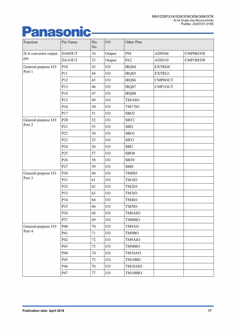
1.4.2 Pin FunctionThe pin function tables of each series are shown in the following order.• Pin function table in MN103SFX7K series (Table 1.4-1 )• Pin function table in MN103SFX6K series (Table 1.4-2 )• Pin function table in MN103SFX5K series (Table 1.4-3 )• Pin function table in MN103SFX3K series (Table 1.4-4 )• Pin function table in MN103SFX2K series (Table 1.4-5 )• Pin function table in MN103SFX1K series (Table 1.4-6 )
Hint:When designing a board, resistor and capacity should be connected to the pins (power supply, GND, function con-trol, clock, reset, on-board debug function, and Unused). Refer to [Chapter Overview] of LSI User's Manual for thevalue of resistor and capacity/
MN103SFX1K/X2K/X3K/X5K/X6K/X7K32-bit Single-chip Microcontroller
PubNo. 232X701-015E
Publication date: April 2018 12

1.4.2.1 Pin Function Table in MN103SFX7K SeriesPin function table in MN103SFX7K series is shown in Table 1.4-1 .
Table 1.4-1 Pin function table in MN103SFX7K series
Function Pin Name PinNo.
I/O Other Pins
Power supply pin fordigital I/O
VDD50 40 Input
65
94
Power supply pin foranalog
AVDD50 17 Input
GND pin for digital VSS 38 Input
67
96
GND pin for analog AVSS 15 Input
Power supply outputpin for internal circuit
VOUT18 42 Output
Test signal input pin NTEST 39 Input
Start sector control pin NBOOT 33 Input
Reset signal input pin(negative logic)
NRST 48 I/O
High-speed oscillationinput pin
OSCI 37 Input
High-speed oscillationoutput pin
OSCO 36 Output
External interruptinput pin
IRQ00 3 Input P80
IRQ01 4 Input P81
IRQ02 5 Input P82
IRQ03 6 Input P83
IRQ04 43 Input P10 EXTRG0
IRQ05 44 Input P11 EXTRG1
IRQ06 45 Input P12 CMP0OUT
IRQ07 46 Input P13 CMP1OUT
IRQ08 47 Input P14
MN103SFX1K/X2K/X3K/X5K/X6K/X7K32-bit Single-chip Microcontroller
PubNo. 232X701-015E
Publication date: April 2018 13

Function Pin Name PinNo.
I/O Other Pins
8-bit timer I/O pin TM0IO 60 I/O P30
TM1IO 61 I/O P31
TM2IO 62 I/O P32
TM3IO 63 I/O P33
TM4IO 64 I/O P34
TM5IO 66 I/O P35
TM6IO 78 I/O P50
TM7IO 79 I/O P51
TM14IO 7 I/O P84
TM15IO 8 I/O P85
TM16IO 49 I/O P15
TM17IO 50 I/O P16
16-bit timer I/O pin TM8AIO 68 I/O P36
TM8BIO 69 I/O P37
TM9AO 70 Output P40
TM9BO 71 Output P41
TM9AIO 72 I/O P42
TM9BIO 73 I/O P43
TM10AO 74 Output P44
TM10BO 75 Output P45
TM10AIO 76 I/O P46
TM10BIO 77 I/O P47
TM11IO0 95 I/O P72
TM11IO1 97 I/O P73
TM11O2 99 Output P74
TM11O3 100 Output P75
TM11O4 1 Output P76
TM11O5 2 Output P77
MN103SFX1K/X2K/X3K/X5K/X6K/X7K32-bit Single-chip Microcontroller
PubNo. 232X701-015E
Publication date: April 2018 14

Function Pin Name PinNo.
I/O Other Pins
Motor control 3-pha-ses PWM signal I/Opin
PWM00 80 Output P52
NPWM00 81 Output P53
PWM01 82 Output P54
NPWM01 83 Output P55
PWM02 84 Output P56
NPWM02 85 Output P57
PWM10 88 Output P62
NPWM10 89 Output P63
PWM11 90 Output P64
NPWM11 91 Output P65
PWM12 92 Output P66
NPWM12 93 Output P67
Serial clock I/O pin SBT0 58 I/O P26
SBT1 55 I/O P23
SBT2 52 I/O P20
SBO0 57 Output P25
SBO1 54 Output P22
SBO2 51 I/O P17
SBI0 59 Input P27
SBI1 56 Input P24
SBI2 53 Input P21
MN103SFX1K/X2K/X3K/X5K/X6K/X7K32-bit Single-chip Microcontroller
PubNo. 232X701-015E
Publication date: April 2018 15

Function Pin Name PinNo.
I/O Other Pins
Analog input pin forA/D converter
ADIN00 11 Input P90 VGA0N CMP0REFA
ADIN01 12 Input P91 VGA0P0 CMP0INA
ADIN02 13 Input P92 VGA0P1
ADIN03 14 Input P93 VGA0P2
ADIN04 16 Input P94 CMP0REFB DA0OUT
ADIN05 18 Input P95 CMP0INB
ADIN06 19 Input P96 VGA1N CMP1REFA
ADIN07 20 Input P97 VGA1P0 CMP1INA
ADIN08 21 Input PA0 VGA1P1
ADIN09 22 Input PA1 VGA1P2
ADIN10 23 Input PA2 CMP1REFB DA1OUT
ADIN11 24 Input PA3 CMP1INB
ADIN12 25 Input PA4
ADIN13 26 Input PA5
ADIN14 27 Input PA6
ADIN15 28 Input PA7
ADIN16 29 Input PB0
ADIN17 30 Input PB1
ADIN18 34 Input PB2
ADIN19 35 Input PB3
Analog input pin forVGA
VGA0N 11 Input P90 ADIN00 CMP0REFA
VGA0P0 12 Input P91 ADIN01 CMP0INA
VGA0P1 13 Input P92 ADIN02
VGA0P2 14 Input P93 ADIN03
VGA1N 19 Input P96 ADIN06 CMP1REFA
VGA1P0 20 Input P97 ADIN07 CMP1INA
VGA1P1 21 Input PA0 ADIN08
VGA1P2 22 Input PA1 ADIN09
Comparator referencevoltage input pin
CMP0REFA 11 Input P90 ADIN00 VGA0N
CMP0REFB 16 Input P94 ADIN04 DA0OUT
CMP1REFA 19 Input P96 ADIN06 VGA1N
CMP1REFB 23 Input PA2 ADIN10 DA1OUT
Comparator input pin CMP0INA 12 Input P91 ADIN01 VGA0P0
CMP0INB 18 Input P95 ADIN05
CMP1INA 20 Input P97 ADIN07 VGA1P0
CMP1INB 24 Input PA3 ADIN11
Comparator output pin CMP0OUT 45 Output P12 IRQ06
CMP1OUT 46 Output P13 IRQ07
MN103SFX1K/X2K/X3K/X5K/X6K/X7K32-bit Single-chip Microcontroller
PubNo. 232X701-015E
Publication date: April 2018 16
Function Pin Name PinNo.
I/O Other Pins
D/A converter outputpin
DA0OUT 16 Output P94 ADIN04 CMP0REFB
DA1OUT 23 Output PA2 ADIN10 CMP1REFB
General-purpose I/OPort 1
P10 43 I/O IRQ04 EXTRG0
P11 44 I/O IRQ05 EXTRG1
P12 45 I/O IRQ06 CMP0OUT
P13 46 I/O IRQ07 CMP1OUT
P14 47 I/O IRQ08
P15 49 I/O TM16IO
P16 50 I/O TM17IO
P17 51 I/O SBO2
General-purpose I/OPort 2
P20 52 I/O SBT2
P21 53 I/O SBI2
P22 54 I/O SBO1
P23 55 I/O SBT1
P24 56 I/O SBI1
P25 57 I/O SBO0
P26 58 I/O SBT0
P27 59 I/O SBI0
General-purpose I/OPort 3
P30 60 I/O TM0IO
P31 61 I/O TM1IO
P32 62 I/O TM2IO
P33 63 I/O TM3IO
P34 64 I/O TM4IO
P35 66 I/O TM5IO
P36 68 I/O TM8AIO
P37 69 I/O TM8BIO
General-purpose I/OPort 4
P40 70 I/O TM9AO
P41 71 I/O TM9BO
P42 72 I/O TM9AIO
P43 73 I/O TM9BIO
P44 74 I/O TM10AO
P45 75 I/O TM10BO
P46 76 I/O TM10AIO
P47 77 I/O TM10BIO
MN103SFX1K/X2K/X3K/X5K/X6K/X7K32-bit Single-chip Microcontroller
PubNo. 232X701-015E
Publication date: April 2018 17

Function Pin Name PinNo.
I/O Other Pins
General-purpose I/OPort 5
P50 78 I/O TM6IO
P51 79 I/O TM7IO
P52 80 I/O PWM00
P53 81 I/O NPWM00
P54 82 I/O PWM01
P55 83 I/O NPWM01
P56 84 I/O PWM02
P57 85 I/O NPWM02
General-purpose I/OPort 6
P60 86 I/O
P61 87 I/O
P62 88 I/O PWM10
P63 89 I/O NPWM10
P64 90 I/O PWM11
P65 91 I/O NPWM11
P66 92 I/O PWM12
P67 93 I/O NPWM12
General-purpose I/OPort 7
P72 95 I/O TM11IO0
P73 97 I/O TM11IO1
P74 99 I/O TM11O2
P75 100 I/O TM11O3
P76 1 I/O TM11O4
P77 2 I/O TM11O5
General-purpose I/OPort 8
P80 3 I/O IRQ00
P81 4 I/O IRQ01
P82 5 I/O IRQ02
P83 6 I/O IRQ03
P84 7 I/O TM14IO
P85 8 I/O TM15IO
P86 9 I/O
P87 10 I/O
General-purpose I/OPort 9
P90 11 Input ADIN00 VGA0N CMP0REFA
P91 12 Input ADIN01 VGA0P0 CMP0INA
P92 13 Input ADIN02 VGA0P1
P93 14 Input ADIN03 VGA0P2
P94 16 I/O ADIN04 CMP0REFB DA0OUT
P95 18 I/O ADIN05 CMP0INB
P96 19 Input ADIN06 VGA1N CMP1REFA
P97 20 Input ADIN07 VGA1P0 CMP1INA
MN103SFX1K/X2K/X3K/X5K/X6K/X7K32-bit Single-chip Microcontroller
PubNo. 232X701-015E
Publication date: April 2018 18

Function Pin Name PinNo.
I/O Other Pins
General-purpose I/OPort A
PA0 21 Input ADIN08 VGA1P1
PA1 22 Input ADIN09 VGA1P2
PA2 23 I/O ADIN10 CMP1REFB DA1OUT
PA3 24 I/O ADIN11 CMP1INB
PA4 25 I/O ADIN12
PA5 26 I/O ADIN13
PA6 27 I/O ADIN14
PA7 28 I/O ADIN15
General-purpose I/OPort B
PB0 29 I/O ADIN16
PB1 30 I/O ADIN17
PB2 34 I/O ADIN18
PB3 35 I/O ADIN19
Clock input pin foron-board debugger
SCLK 31 Input
Data I/O pin for on-board debugger
SDATA 32 I/O
Trigger I/O pin for on-board debugger
EXTRG0 43 I/O P10 IRQ04
EXTRG1 44 I/O P11 IRQ05
MN103SFX1K/X2K/X3K/X5K/X6K/X7K32-bit Single-chip Microcontroller
PubNo. 232X701-015E
Publication date: April 2018 19

1.4.2.2 Pin Function Table in MN103SFX6K SeriesPin function table in MN103SFX6K series is shown in Table 1.4-2 .
Table 1.4-2 Pin function table in MN103SFX6K series
Function Pin Name PinNo.
I/O Other Pins
Power supply pin for digi-tal I/O
VDD50 31 Input
54
76
Power supply pin for ana-log
AVDD50 12 Input
GND pin for digital VSS 29 Input
56
78
GND pin for analog AVSS 10 Input
Power supply output pinfor internal circuit
VOUT18 33 Output
Test signal input pin NTEST 30 Input
Start sector control pin NBOOT 26 Input
Reset signal input pin(negative logic)
NRST 39 I/O
High-speed oscillationinput pin
OSCI 28 Input
High-speed oscillationoutput pin
OSCO 27 Output
External interrupt inputpin
IRQ00 1 Input P80
IRQ01 2 Input P81
IRQ02 3 Input P82
IRQ03 4 Input P83
IRQ04 34 Input P10 EXTRG0
IRQ05 35 Input P11 EXTRG1
IRQ06 36 Input P12 CMP0OUT
IRQ07 37 Input P13 CMP1OUT
IRQ08 38 Input P14
8-bit timer I/O pin TM1IO 50 I/O P31
TM2IO 51 I/O P32
TM3IO 52 I/O P33
TM4IO 53 I/O P34
TM5IO 55 I/O P35
TM7IO 63 I/O P51
TM15IO 5 I/O P85
TM17IO 40 I/O P16
MN103SFX1K/X2K/X3K/X5K/X6K/X7K32-bit Single-chip Microcontroller
PubNo. 232X701-015E
Publication date: April 2018 20

Function Pin Name PinNo.
I/O Other Pins
16-bit timer I/O pin TM8AIO 57 I/O P36
TM8BIO 58 I/O P37
TM9AIO 59 I/O P42
TM9BIO 60 I/O P43
TM10AIO 61 I/O P46
TM10BIO 62 I/O P47
TM11IO0 77 I/O P72
TM11IO1 79 I/O P73
Motor control 3-phasesPWM signal I/O pin
PWM00 64 Output P52
NPWM00 65 Output P53
PWM01 66 Output P54
NPWM01 67 Output P55
PWM02 68 Output P56
NPWM02 69 Output P57
PWM10 70 Output P62
NPWM10 71 Output P63
PWM11 72 Output P64
NPWM11 73 Output P65
PWM12 74 Output P66
NPWM12 75 Output P67
Serial clock I/O pin SBT0 48 I/O P26
SBT1 45 I/O P23
SBT2 42 I/O P20
SBO0 47 Output P25
SBO1 44 Output P22
SBO2 41 I/O P17
SBI0 49 Input P27
SBI1 46 Input P24
SBI2 43 Input P21
MN103SFX1K/X2K/X3K/X5K/X6K/X7K32-bit Single-chip Microcontroller
PubNo. 232X701-015E
Publication date: April 2018 21

Function Pin Name PinNo.
I/O Other Pins
Analog input pin for A/Dconverter
ADIN00 6 Input P90 VGA0N CMP0REFA
ADIN01 7 Input P91 VGA0P0 CMP0INA
ADIN02 8 Input P92 VGA0P1
ADIN03 9 Input P93 VGA0P2
ADIN04 11 Input P94 CMP0REFB DA0OUT
ADIN05 13 Input P95 CMP0INB
ADIN06 14 Input P96 VGA1N CMP1REFA
ADIN07 15 Input P97 VGA1P0 CMP1INA
ADIN08 16 Input PA0 VGA1P1
ADIN09 17 Input PA1 VGA1P2
ADIN10 18 Input PA2 CMP1REFB DA1OUT
ADIN11 19 Input PA3 CMP1INB
ADIN12 20 Input PA4
ADIN13 21 Input PA5
ADIN14 22 Input PA6
ADIN15 23 Input PA7
Analog input pin for VGA VGA0N 6 Input P90 ADIN00 CMP0REFA
VGA0P0 7 Input P91 ADIN01 CMP0INA
VGA0P1 8 Input P92 ADIN02
VGA0P2 9 Input P93 ADIN03
VGA1N 14 Input P96 ADIN06 CMP1REFA
VGA1P0 15 Input P97 ADIN07 CMP1INA
VGA1P1 16 Input PA0 ADIN08
VGA1P2 17 Input PA1 ADIN09
Comparator referencevoltage input pin
CMP0REFA 6 Input P90 ADIN00 VGA0N
CMP0REFB 11 Input P94 ADIN04 DA0OUT
CMP1REFA 14 Input P96 ADIN06 VGA1N
CMP1REFB 18 Input PA2 ADIN10 DA1OUT
Comparator input pin CMP0INA 7 Input P91 ADIN01 VGA0P0
CMP0INB 13 Input P95 ADIN05
CMP1INA 15 Input P97 ADIN07 VGA1P0
CMP1INB 19 Input PA3 ADIN11
Comparator output pin CMP0OUT 36 Output P12 IRQ06
CMP1OUT 37 Output P13 IRQ07
D/A converter output pin DA0OUT 11 Output P94 ADIN04 CMP0REFB
DA1OUT 18 Output PA2 ADIN10 CMP1REFB
MN103SFX1K/X2K/X3K/X5K/X6K/X7K32-bit Single-chip Microcontroller
PubNo. 232X701-015E
Publication date: April 2018 22

Function Pin Name PinNo.
I/O Other Pins
General-purpose I/O Port1
P10 34 I/O IRQ04 EXTRG0
P11 35 I/O IRQ05 EXTRG1
P12 36 I/O IRQ06 CMP0OUT
P13 37 I/O IRQ07 CMP1OUT
P14 38 I/O IRQ08
P16 40 I/O TM17IO
P17 41 I/O SBO2
General-purpose I/O Port2
P20 42 I/O SBT2
P21 43 I/O SBI2
P22 44 I/O SBO1
P23 45 I/O SBT1
P24 46 I/O SBI1
P25 47 I/O SBO0
P26 48 I/O SBT0
P27 49 I/O SBI0
General-purpose I/O Port3
P31 50 I/O TM1IO
P32 51 I/O TM2IO
P33 52 I/O TM3IO
P34 53 I/O TM4IO
P35 55 I/O TM5IO
P36 57 I/O TM8AIO
P37 58 I/O TM8BIO
General-purpose I/O Port4
P42 59 I/O TM9AIO
P43 60 I/O TM9BIO
P46 61 I/O TM10AIO
P47 62 I/O TM10BIO
General-purpose I/O Port5
P51 63 I/O TM7IO
P52 64 I/O PWM00
P53 65 I/O NPWM00
P54 66 I/O PWM01
P55 67 I/O NPWM01
P56 68 I/O PWM02
P57 69 I/O NPWM02
MN103SFX1K/X2K/X3K/X5K/X6K/X7K32-bit Single-chip Microcontroller
PubNo. 232X701-015E
Publication date: April 2018 23

Function Pin Name PinNo.
I/O Other Pins
General-purpose I/O Port6
P62 70 I/O PWM10
P63 71 I/O NPWM10
P64 72 I/O PWM11
P65 73 I/O NPWM11
P66 74 I/O PWM12
P67 75 I/O NPWM12
General-purpose I/O Port7
P72 77 I/O TM11IO0
P73 79 I/O TM11IO1
General-purpose I/O Port8
P80 1 I/O IRQ00
P81 2 I/O IRQ01
P82 3 I/O IRQ02
P83 4 I/O IRQ03
P85 5 I/O TM15IO
General-purpose I/O Port9
P90 6 Input ADIN00 VGA0N CMP0REFA
P91 7 Input ADIN01 VGA0P0 CMP0INA
P92 8 Input ADIN02 VGA0P1
P93 9 Input ADIN03 VGA0P2
P94 11 I/O ADIN04 CMP0REFB DA0OUT
P95 13 I/O ADIN05 CMP0IN
P96 14 Input ADIN06 VGA1N CMP1REFA
P97 15 Input ADIN07 VGA1P0 CMP1INA
General-purpose I/O PortA
PA0 16 Input ADIN08 VGA1P1
PA1 17 Input ADIN09 VGA1P2
PA2 18 I/O ADIN10 CMP1REFB DA1OUT
PA3 19 I/O ADIN11 CMP1INB
PA4 20 I/O ADIN12
PA5 21 I/O ADIN13
PA6 22 I/O ADIN14
PA7 23 I/O ADIN15
Clock input pin for on-board debugger
SCLK 24 Input
Data I/O pin for on-boarddebugger
SDATA 25 I/O
Trigger I/O pin for on-board debugger
EXTRG0 34 I/O P10 IRQ04
EXTRG1 35 I/O P11 IRQ05
MN103SFX1K/X2K/X3K/X5K/X6K/X7K32-bit Single-chip Microcontroller
PubNo. 232X701-015E
Publication date: April 2018 24

1.4.2.3 Pin Function Table in MN103SFX5K SeriesPin function table in MN103SFX5K series is shown in Table 1.4-3 .
Table 1.4-3 Pin function table in MN103SFX5K series
Function Pin Name PinNo.
I/O Other Pins
Power supply pin fordigital I/O
VDD50 25 Input
60
Power supply pin foranalog
AVDD50 10 Input
GND pin for digital VSS 23 Input
62
GND pin for analog AVSS 8 Input
Power supply outputpin for internal circuit
VOUT18 26 Output
Test signal input pin NTEST 24 Input
Start sector controlpin
NBOOT 20 Input
Reset signal input pin(negative logic)
NRST 31 I/O
High-speed oscillationinput pin
OSCI 22 Input
High-speed oscillationoutput pin
OSCO 21 Output
External interruptinput pin
IRQ00 64 Input P80
IRQ01 1 Input P81
IRQ02 2 Input P82
IRQ03 3 Input P83
IRQ04 27 Input P10 EXTRG0
IRQ05 28 Input P11 EXTRG1
IRQ06 29 Input P12 CMP0OUT
IRQ07 30 Input P13 CMP1OUT
8-bit timer I/O pin TM1IO 41 I/O P31
TM2IO 42 I/O P32
TM3IO 43 I/O P33
TM4IO 44 I/O P34
TM5IO 45 I/O P35
16-bit timer I/O pin TM9AIO 46 I/O P42
TM9BIO 47 I/O P43
TM10AIO 48 I/O P46
TM10BIO 49 I/O P47
MN103SFX1K/X2K/X3K/X5K/X6K/X7K32-bit Single-chip Microcontroller
PubNo. 232X701-015E
Publication date: April 2018 25

Function Pin Name PinNo.
I/O Other Pins
Motor control 3-pha-ses PWM signal I/Opin
PWM00 50 Output P52
NPWM00 51 Output P53
PWM01 52 Output P54
NPWM01 53 Output P55
PWM02 54 Output P56
NPWM02 55 Output P57
PWM10 56 Output P62
NPWM10 57 Output P63
PWM11 58 Output P64
NPWM11 59 Output P65
PWM12 61 Output P66
NPWM12 63 Output P67
Serial clock I/O pin SBT0 39 I/O P26
SBT1 36 I/O P23
SBT2 33 I/O P20
SBO0 38 Output P25
SBO1 35 Output P22
SBO2 32 I/O P17
SBI0 40 Input P27
SBI1 37 Input P24
SBI2 34 Input P21
Analog input pin forA/D converter
ADIN00 4 Input P90 VGA0N CMP0REFA
ADIN01 5 Input P91 VGA0P0 CMP0INA
ADIN02 6 Input P92 VGA0P1
ADIN03 7 Input P93 VGA0P2
ADIN04 9 Input P94 CMP0REFB DA0OUT
ADIN05 11 Input P95 CMP0INB
ADIN06 12 Input P96 VGA1N CMP1REFA
ADIN07 13 Input P97 VGA1P0 CMP1INA
ADIN08 14 Input PA0 VGA1P1
ADIN09 15 Input PA1 VGA1P2
ADIN10 16 Input PA2 CMP1REFB DA1OUT
ADIN11 17 Input PA3 CMP1INB
MN103SFX1K/X2K/X3K/X5K/X6K/X7K32-bit Single-chip Microcontroller
PubNo. 232X701-015E
Publication date: April 2018 26

Function Pin Name PinNo.
I/O Other Pins
Analog input pin forVGA
VGA0N 4 Input P90 ADIN00 CMP0REFA
VGA0P0 5 Input P91 ADIN01 CMP0INA
VGA0P1 6 Input P92 ADIN02
VGA0P2 7 Input P93 ADIN03
VGA1N 12 Input P96 ADIN06 CMP1REFA
VGA1P0 13 Input P97 ADIN07 CMP1INA
VGA1P1 14 Input PA0 ADIN08
VGA1P2 15 Input PA1 ADIN09
Comparator referencevoltage input pin
CMP0REFA 4 Input P90 ADIN00 VGA0N
CMP0REFB 9 Input P94 ADIN04 DA0OUT
CMP1REFA 12 Input P96 ADIN06 VGA1N
CMP1REFB 16 Input PA2 ADIN10 DA1OUT
Comparator input pin CMP0INA 5 Input P91 ADIN01 VGA0P0
CMP0INB 11 Input P95 ADIN05
CMP1INA 13 Input P97 ADIN07 VGA1P0
CMP1INB 17 Input PA3 ADIN11
Comparator output pin CMP0OUT 29 Output P12 IRQ06
CMP1OUT 30 Output P13 IRQ07
D/A converter outputpin
DA0OUT 9 Output P94 ADIN04 CMP0REFB
DA1OUT 16 Output PA2 ADIN10 CMP1REFB
General-purpose I/OPort 1
P10 27 I/O IRQ04 EXTRG0
P11 28 I/O IRQ05 EXTRG1
P12 29 I/O IRQ06 CMP0OUT
P13 30 I/O IRQ07 CMP1OUT
P17 32 I/O SBO2
General-purpose I/OPort 2
P20 33 I/O SBT2
P21 34 I/O SBI2
P22 35 I/O SBO1 s
P23 36 I/O SBT1
P24 37 I/O SBI1
P25 38 I/O SBO0
P26 39 I/O SBT0
P27 40 I/O SBI0
General-purpose I/OPort 3
P31 41 I/O TM1IO
P32 42 I/O TM2IO
P33 43 I/O TM3IO
P34 44 I/O TM4IO
P35 45 I/O TM5IO
MN103SFX1K/X2K/X3K/X5K/X6K/X7K32-bit Single-chip Microcontroller
PubNo. 232X701-015E
Publication date: April 2018 27

Function Pin Name PinNo.
I/O Other Pins
General-purpose I/OPort 4
P42 46 I/O TM9AIO
P43 47 I/O TM9BIO
P46 48 I/O TM10AIO
P47 49 I/O TM10BIO
General-purpose I/OPort 5
P52 50 I/O PWM00
P53 51 I/O NPWM00
P54 52 I/O PWM01
P55 53 I/O NPWM01
P56 54 I/O PWM02
P57 55 I/O NPWM02
General-purpose I/OPort 6
P62 56 I/O PWM10
P63 57 I/O NPWM10
P64 58 I/O PWM11
P65 59 I/O NPWM11
P66 61 I/O PWM12
P67 63 I/O NPWM12
General-purpose I/OPort 8
P80 64 I/O IRQ00
P81 1 I/O IRQ01
P82 2 I/O IRQ02
P83 3 I/O IRQ03
General-purpose I/OPort 9
P90 4 Input ADIN00 VGA0N CMP0REFA
P91 5 Input ADIN01 VGA0P0 CMP0INA
P92 6 Input ADIN02 VGA0P1
P93 7 Input ADIN03 VGA0P2
P94 9 I/O ADIN04 CMP0REFB DA0OUT
P95 11 I/O ADIN05 CMP0INB
P96 12 Input ADIN06 VGA1N CMP1REFA
P97 13 Input ADIN07 VGA1P0 CMP1INA
General-purpose I/OPort A
PA0 14 Input ADIN08 VGA1P1
PA1 15 Input ADIN09 VGA1P2
PA2 16 I/O ADIN10 CMP1REFB DA1OUT
PA3 17 I/O ADIN11 CMP1INB
Clock input pin foron-board debugger
SCLK 18 Input
Data I/O pin for on-board debugger
SDATA 19 I/O
Trigger I/O pin for on-board debugger
EXTRG0 27 I/O P10 IRQ04
EXTRG1 28 I/O P11 IRQ05
MN103SFX1K/X2K/X3K/X5K/X6K/X7K32-bit Single-chip Microcontroller
PubNo. 232X701-015E
Publication date: April 2018 28

1.4.2.4 Pin Function Table in MN103SFX3K SeriesPin function table in MN103SFX3K series is shown in Table 1.4-4 .
Table 1.4-4 Pin function table in MN103SFX3K series
Function Pin Name Pin No. I/O Other Pins
Power supply pin fordigital I/O
VDD50 40 Input
65
94
Power supply pin foranalog
AVDD50 17 Input
GND pin for digital VSS 38 Input
67
96
GND pin for analog AVSS 15 Input
Power supply outputpin for internal circuit
VOUT18 42 Output
Test signal input pin NTEST 39 Input
Start sector control pin NBOOT 33 Input
Reset signal input pin(negative logic)
NRST 48 I/O
High-speed oscillationinput pin
OSCI 37 Input
High-speed oscillationoutput pin
OSCO 36 Output
External interruptinput pin
IRQ00 3 Input P80
IRQ01 4 Input P81
IRQ02 5 Input P82
IRQ03 6 Input P83
IRQ04 43 Input P10 EXTRG0
IRQ05 44 Input P11 EXTRG1
IRQ06 45 Input P12 CMP0OUT
IRQ07 46 Input P13 CMP1OUT
IRQ08 47 Input P14
MN103SFX1K/X2K/X3K/X5K/X6K/X7K32-bit Single-chip Microcontroller
PubNo. 232X701-015E
Publication date: April 2018 29

Function Pin Name Pin No. I/O Other Pins
8-bit timer I/O pin TM0IO 60 I/O P30
TM1IO 61 I/O P31
TM2IO 62 I/O P32
TM3IO 63 I/O P33
TM4IO 64 I/O P34
TM5IO 66 I/O P35
TM6IO 78 I/O P50
TM7IO 79 I/O P51
TM14IO 7 I/O P84
TM15IO 8 I/O P85
TM16IO 49 I/O P15
TM17IO 50 I/O P16
16-bit timer I/O pin TM8AIO 68 I/O P36
TM8BIO 69 I/O P37
TM9AO 70 Output P40
TM9BO 71 Output P41
TM9AIO 72 I/O P42
TM9BIO 73 I/O P43
TM10AO 74 Output P44
TM10BO 75 Output P45
TM10AIO 76 I/O P46
TM10BIO 77 I/O P47
TM11IO0 95 I/O P72
TM11IO1 97 I/O P73
TM11O2 99 Output P74
TM11O3 100 Output P75
TM11O4 1 Output P76
TM11O5 2 Output P77
MN103SFX1K/X2K/X3K/X5K/X6K/X7K32-bit Single-chip Microcontroller
PubNo. 232X701-015E
Publication date: April 2018 30

Function Pin Name Pin No. I/O Other Pins
Motor control 3-pha-ses PWM signal I/Opin
PWM00 80 Output P52
NPWM00 81 Output P53
PWM01 82 Output P54
NPWM01 83 Output P55
PWM02 84 Output P56
NPWM02 85 Output P57
PWM10 88 Output P62
NPWM10 89 Output P63
PWM11 90 Output P64
NPWM11 91 Output P65
PWM12 92 Output P66
NPWM12 93 Output P67
Serial clock I/O pin SBT0 58 I/O P26
SBT1 55 I/O P23
SBT2 52 I/O P20
SBO0 57 Output P25
SBO1 54 Output P22
SBO2 51 I/O P17
SBI0 59 Input P27
SBI1 56 Input P24
SBI2 53 Input P21
MN103SFX1K/X2K/X3K/X5K/X6K/X7K32-bit Single-chip Microcontroller
PubNo. 232X701-015E
Publication date: April 2018 31

Function Pin Name Pin No. I/O Other Pins
Analog input pin forA/D converter
ADIN00 11 Input P90
ADIN01 12 Input P91
ADIN02 13 Input P92
ADIN03 14 Input P93
ADIN04 16 Input P94 CMP0REF DA0OUT
ADIN05 18 Input P95 CMP0IN
ADIN06 19 Input P96
ADIN07 20 Input P97
ADIN08 21 Input PA0
ADIN09 22 Input PA1
ADIN10 23 Input PA2 CMP1REF DA1OUT
ADIN11 24 Input PA3 CMP1IN
ADIN12 25 Input PA4
ADIN13 26 Input PA5
ADIN14 27 Input PA6
ADIN15 28 Input PA7
ADIN16 29 Input PB0
ADIN17 30 Input PB1
ADIN18 34 Input PB2
ADIN19 35 Input PB3
Comparator referencevoltage input pin
CMP0REF 16 Input P94 ADIN04 DA0OUT
CMP1REF 23 Input PA2 ADIN10 DA1OUT
Comparator input pin CMP0IN 18 Input P95 ADIN05
CMP1IN 24 Input PA3 ADIN11
Comparator output pin CMP0OUT 45 Output P12 IRQ06
CMP1OUT 46 Output P13 IRQ07
D/A converter outputpin
DA0OUT 16 Output P94 ADIN04 CMP0REF
DA1OUT 23 Output PA2 ADIN10 CMP1REF
General-purpose I/OPort 1
P10 43 I/O IRQ04 EXTRG0
P11 44 I/O IRQ05 EXTRG1
P12 45 I/O IRQ06 CMP0OUT
P13 46 I/O IRQ07 CMP1OUT
P14 47 I/O IRQ08
P15 49 I/O TM16IO
P16 50 I/O TM17IO
P17 51 I/O SBO2
MN103SFX1K/X2K/X3K/X5K/X6K/X7K32-bit Single-chip Microcontroller
PubNo. 232X701-015E
Publication date: April 2018 32
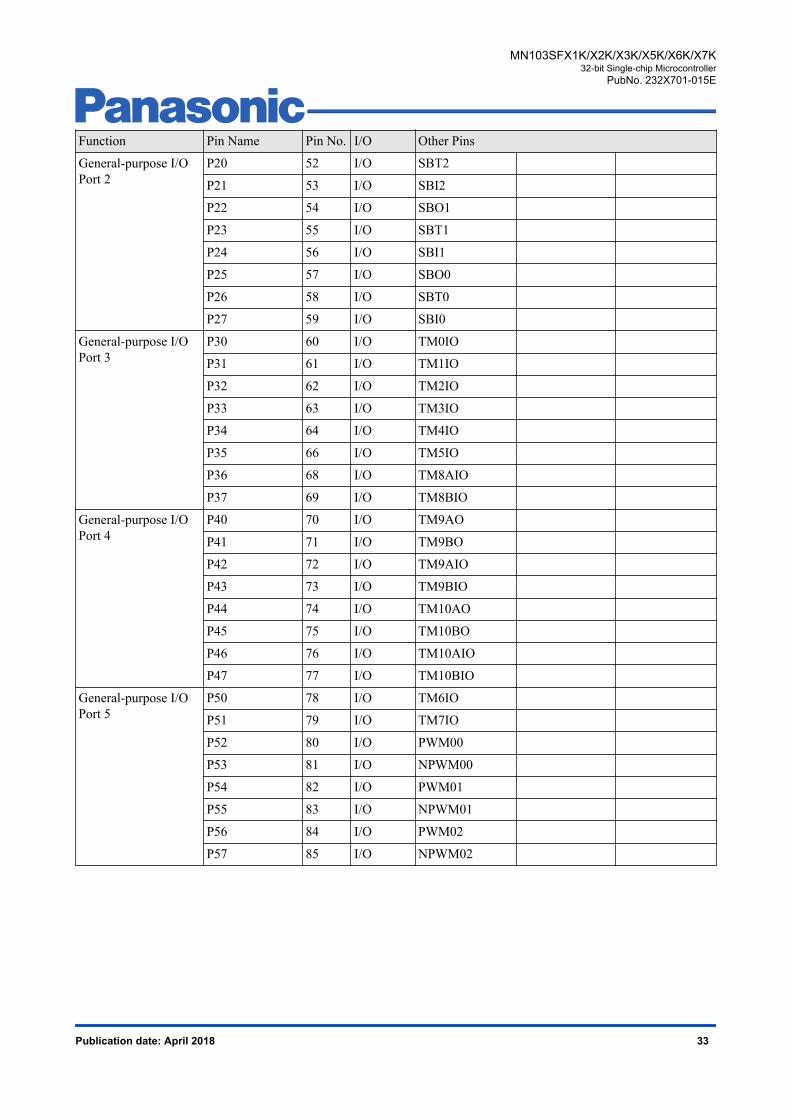
Function Pin Name Pin No. I/O Other Pins
General-purpose I/OPort 2
P20 52 I/O SBT2
P21 53 I/O SBI2
P22 54 I/O SBO1
P23 55 I/O SBT1
P24 56 I/O SBI1
P25 57 I/O SBO0
P26 58 I/O SBT0
P27 59 I/O SBI0
General-purpose I/OPort 3
P30 60 I/O TM0IO
P31 61 I/O TM1IO
P32 62 I/O TM2IO
P33 63 I/O TM3IO
P34 64 I/O TM4IO
P35 66 I/O TM5IO
P36 68 I/O TM8AIO
P37 69 I/O TM8BIO
General-purpose I/OPort 4
P40 70 I/O TM9AO
P41 71 I/O TM9BO
P42 72 I/O TM9AIO
P43 73 I/O TM9BIO
P44 74 I/O TM10AO
P45 75 I/O TM10BO
P46 76 I/O TM10AIO
P47 77 I/O TM10BIO
General-purpose I/OPort 5
P50 78 I/O TM6IO
P51 79 I/O TM7IO
P52 80 I/O PWM00
P53 81 I/O NPWM00
P54 82 I/O PWM01
P55 83 I/O NPWM01
P56 84 I/O PWM02
P57 85 I/O NPWM02
MN103SFX1K/X2K/X3K/X5K/X6K/X7K32-bit Single-chip Microcontroller
PubNo. 232X701-015E
Publication date: April 2018 33

Function Pin Name Pin No. I/O Other Pins
General-purpose I/OPort 6
P60 86 I/O
P61 87 I/O
P62 88 I/O PWM10
P63 89 I/O NPWM10
P64 90 I/O PWM11
P65 91 I/O NPWM11
P66 92 I/O PWM12
P67 93 I/O NPWM12
General-purpose I/OPort 7
P72 95 I/O TM11IO0
P73 97 I/O TM11IO1
P74 99 I/O TM11O2
P75 100 I/O TM11O3
P76 1 I/O TM11O4
P77 2 I/O TM11O5
General-purpose I/OPort 8
P80 3 I/O IRQ00
P81 4 I/O IRQ01
P82 5 I/O IRQ02
P83 6 I/O IRQ03
P84 7 I/O TM14IO
P85 8 I/O TM15IO
P86 9 I/O
P87 10 I/O
General-purpose I/OPort 9
P90 11 I/O ADIN00
P91 12 I/O ADIN01
P92 13 I/O ADIN02
P93 14 I/O ADIN03
P94 16 I/O ADIN04 CMP0REF DA0OUT
P95 18 I/O ADIN05 CMP0IN
P96 19 I/O ADIN06
P97 20 I/O ADIN07
General-purpose I/OPort A
PA0 21 I/O ADIN08
PA1 22 I/O ADIN09
PA2 23 I/O ADIN10 CMP1REF DA1OUT
PA3 24 I/O ADIN11 CMP1IN
PA4 25 I/O ADIN12
PA5 26 I/O ADIN13
PA6 27 I/O ADIN14
PA7 28 I/O ADIN15
MN103SFX1K/X2K/X3K/X5K/X6K/X7K32-bit Single-chip Microcontroller
PubNo. 232X701-015E
Publication date: April 2018 34

Function Pin Name Pin No. I/O Other Pins
General-purpose I/OPort B
PB0 29 I/O ADIN16
PB1 30 I/O ADIN17
PB2 34 I/O ADIN18
PB3 35 I/O ADIN19
Clock input pin foron-board debugger
SCLK 31 Input
Data I/O pin for on-board debugger
SDATA 32 I/O
Trigger I/O pin for on-board debugger
EXTRG0 43 I/O P10 IRQ04
EXTRG1 44 I/O P11 IRQ05
MN103SFX1K/X2K/X3K/X5K/X6K/X7K32-bit Single-chip Microcontroller
PubNo. 232X701-015E
Publication date: April 2018 35

1.4.2.5 Pin Function Table in MN103SFX2K SeriesPin function table in MN103SFX2K series is shown in Table 1.4-5 .
Table 1.4-5 Pin function table in MN103SFX3K series
Function Pin Name PinNo.
I/O Other Pins
Power supply pin fordigital I/O
VDD50 31 Input
54
76
Power supply pin foranalog
AVDD50 12 Input
GND pin for digital VSS 29 Input
56
78
GND pin for analog AVSS 10 Input
Power supply outputpin for internal circuit
VOUT18 33 Output
Test signal input pin NTEST 30 Input
Start sector control pin NBOOT 26 Input
Reset signal input pin(negative logic)
NRST 39 I/O
High-speed oscillationinput pin
OSCI 28 Input
High-speed oscillationoutput pin
OSCO 27 Output
External interruptinput pin
IRQ00 1 Input P80
IRQ01 2 Input P81
IRQ02 3 Input P82
IRQ03 4 Input P83
IRQ04 34 Input P10 EXTRG0
IRQ05 35 Input P11 EXTRG1
IRQ06 36 Input P12 CMP0OUT
IRQ07 37 Input P13 CMP1OUT
IRQ08 38 Input P14
8-bit timer I/O pin TM1IO 50 I/O P31
TM2IO 51 I/O P32
TM3IO 52 I/O P33
TM4IO 53 I/O P34
TM5IO 55 I/O P35
TM7IO 63 I/O P51
TM15IO 5 I/O P85
TM17IO 40 I/O P16
MN103SFX1K/X2K/X3K/X5K/X6K/X7K32-bit Single-chip Microcontroller
PubNo. 232X701-015E
Publication date: April 2018 36

Function Pin Name PinNo.
I/O Other Pins
16-bit timer I/O pin TM8AIO 57 I/O P36
TM8BIO 58 I/O P37
TM9AIO 59 I/O P42
TM9BIO 60 I/O P43
TM10AIO 61 I/O P46
TM10BIO 62 I/O P47
TM11IO0 77 I/O P72
TM11IO1 79 I/O P73
Motor control 3-pha-ses PWM signal I/Opin
PWM00 64 Output P52
NPWM00 65 Output P53
PWM01 66 Output P54
NPWM01 67 Output P55
PWM02 68 Output P56
NPWM02 69 Output P57
PWM10 70 Output P62
NPWM10 71 Output P63
PWM11 72 Output P64
NPWM11 73 Output P65
PWM12 74 Output P66
NPWM12 75 Output P67
Serial clock I/O pin SBT0 48 I/O P26
SBT1 45 I/O P23
SBT2 42 I/O P20
SBO0 47 Output P25
SBO1 44 Output P22
SBO2 41 I/O P17
SBI0 49 Input P27
SBI1 46 Input P24
SBI2 43 Input P21
MN103SFX1K/X2K/X3K/X5K/X6K/X7K32-bit Single-chip Microcontroller
PubNo. 232X701-015E
Publication date: April 2018 37

Function Pin Name PinNo.
I/O Other Pins
Analog input pin forA/D converter
ADIN00 6 Input P90
ADIN01 7 Input P91
ADIN02 8 Input P92
ADIN03 9 Input P93
ADIN04 11 Input P94 CMP0REF DA0OUT
ADIN05 13 Input P95 CMP0IN
ADIN06 14 Input P96
ADIN07 15 Input P97
ADIN08 16 Input PA0
ADIN09 17 Input PA1
ADIN10 18 Input PA2 CMP1REF DA1OUT
ADIN11 19 Input PA3 CMP1IN
ADIN12 20 Input PA4
ADIN13 21 Input PA5
ADIN14 22 Input PA6
ADIN15 23 Input PA7
Comparator referencevoltage input pin
CMP0REF 11 Input P94 ADIN04 DA0OUT
CMP1REF 18 Input PA2 ADIN10 DA1OUT
Comparator input pin CMP0IN 13 Input P95 ADIN05
CMP1IN 19 Input PA3 ADIN11
Comparator output pin CMP0OUT 36 Output P12 IRQ06
CMP1OUT 37 Output P13 IRQ07
D/A converter outputpin
DA0OUT 11 Output P94 ADIN04 CMP0REF
DA1OUT 18 Output PA2 ADIN10 CMP1REF
General-purpose I/OPort 1
P10 34 I/O IRQ04 EXTRG0
P11 35 I/O IRQ05 EXTRG1
P12 36 I/O IRQ06 CMP0OUT
P13 37 I/O IRQ07 CMP1OUT
P14 38 I/O IRQ08
P16 40 I/O TM17IO
P17 41 I/O SBO2
MN103SFX1K/X2K/X3K/X5K/X6K/X7K32-bit Single-chip Microcontroller
PubNo. 232X701-015E
Publication date: April 2018 38

Function Pin Name PinNo.
I/O Other Pins
General-purpose I/OPort 2
P20 42 I/O SBT2
P21 43 I/O SBI2
P22 44 I/O SBO1
P23 45 I/O SBT1
P24 46 I/O SBI1
P25 47 I/O SBO0
P26 48 I/O SBT0
P27 49 I/O SBI0
General-purpose I/OPort 3
P31 50 I/O TM1IO
P32 51 I/O TM2IO
P33 52 I/O TM3IO
P34 53 I/O TM4IO
P35 55 I/O TM5IO
P36 57 I/O TM8AIO
P37 58 I/O TM8BIO
General-purpose I/OPort 4
P42 59 I/O TM9AIO
P43 60 I/O TM9BIO
P46 61 I/O TM10AIO
P47 62 I/O TM10BIO
General-purpose I/OPort 5
P51 63 I/O TM7IO
P52 64 I/O PWM00
P53 65 I/O NPWM00
P54 66 I/O PWM01
P55 67 I/O NPWM01
P56 68 I/O PWM02
P57 69 I/O NPWM02
General-purpose I/OPort 6
P62 70 I/O PWM10
P63 71 I/O NPWM10
P64 72 I/O PWM11
P65 73 I/O NPWM11
P66 74 I/O PWM12
P67 75 I/O NPWM12
General-purpose I/OPort 7
P72 77 I/O TM11IO0
P73 79 I/O TM11IO1
MN103SFX1K/X2K/X3K/X5K/X6K/X7K32-bit Single-chip Microcontroller
PubNo. 232X701-015E
Publication date: April 2018 39

Function Pin Name PinNo.
I/O Other Pins
General-purpose I/OPort 8
P80 1 I/O IRQ00
P81 2 I/O IRQ01
P82 3 I/O IRQ02
P83 4 I/O IRQ03
P85 5 I/O TM15IO
General-purpose I/OPort 9
P90 6 I/O ADIN00
P91 7 I/O ADIN01
P92 8 I/O ADIN02
P93 9 I/O ADIN03
P94 11 I/O ADIN04 CMP0REF DA0OUT
P95 13 I/O ADIN05 CMP0IN
P96 14 I/O ADIN06
P97 15 I/O ADIN07
General-purpose I/OPort A
PA0 16 I/O ADIN08
PA1 17 I/O ADIN09
PA2 18 I/O ADIN10 CMP1REF DA1OUT
PA3 19 I/O ADIN11 CMP1IN
PA4 20 I/O ADIN12
PA5 21 I/O ADIN13
PA6 22 I/O ADIN14
PA7 23 I/O ADIN15
Clock input pin foron-board debugger
SCLK 24 Input
Data I/O pin for on-board debugger
SDATA 25 I/O
Trigger I/O pin for on-board debugger
EXTRG0 34 I/O P10 IRQ04
EXTRG1 35 I/O P11 IRQ05
MN103SFX1K/X2K/X3K/X5K/X6K/X7K32-bit Single-chip Microcontroller
PubNo. 232X701-015E
Publication date: April 2018 40

1.4.2.6 Pin Function Table in MN103SFX1K SeriesPin function table in MN103SFX1K series is shown in Table 1.4-6 .
Table 1.4-6 Pin function table in MN103SFX1K series
Function Pin Name PinNo.
I/O Other Pins
Power supply pin fordigital I/O
VDD50 25 Input
60
Power supply pin foranalog
AVDD50 10 Input
GND pin for digital VSS 23 Input
62
GND pin for analog AVSS 8 Input
Power supply outputpin for internal circuit
VOUT18 26 Output
Test signal input pin NTEST 24 Input
Start sector controlpin
NBOOT 20 Input
Reset signal input pin(negative logic)
NRST 31 I/O
High-speed oscillationinput pin
OSCI 22 Input
High-speed oscillationoutput pin
OSCO 21 Output
External interruptinput pin
IRQ00 64 Input P80
IRQ01 1 Input P81
IRQ02 2 Input P82
IRQ03 3 Input P83
IRQ04 27 Input P10 EXTRG0
IRQ05 28 Input P11 EXTRG1
IRQ06 29 Input P12 CMP0OUT
IRQ07 30 Input P13 CMP1OUT
8-bit timer I/O pin TM1IO 41 I/O P31
TM2IO 42 I/O P32
TM3IO 43 I/O P33
TM4IO 44 I/O P34
TM5IO 45 I/O P35
16-bit timer I/O pin TM9AIO 46 I/O P42
TM9BIO 47 I/O P43
TM10AIO 48 I/O P46
TM10BIO 49 I/O P47
MN103SFX1K/X2K/X3K/X5K/X6K/X7K32-bit Single-chip Microcontroller
PubNo. 232X701-015E
Publication date: April 2018 41

Function Pin Name PinNo.
I/O Other Pins
Motor control 3-pha-ses PWM signal I/Opin
PWM00 50 Output P52
NPWM00 51 Output P53
PWM01 52 Output P54
NPWM01 53 Output P55
PWM02 54 Output P56
NPWM02 55 Output P57
PWM10 56 Output P62
NPWM10 57 Output P63
PWM11 58 Output P64
NPWM11 59 Output P65
PWM12 61 Output P66
NPWM12 63 Output P67
Serial clock I/O pin SBT0 39 I/O P26
SBT1 36 I/O P23
SBT2 33 I/O P20
SBO0 38 Output P25
SBO1 35 Output P22
SBO2 32 I/O P17
SBI0 40 Input P27
SBI1 37 Input P24
SBI2 34 Input P21
Analog input pin forA/D converter
ADIN00 4 Input P90
ADIN01 5 Input P91
ADIN02 6 Input P92
ADIN03 7 Input P93
ADIN04 9 Input P94 CMP0REF DA0OUT
ADIN05 11 Input P95 CMP0IN
ADIN06 12 Input P96
ADIN07 13 Input P97
ADIN08 14 Input PA0
ADIN09 15 Input PA1
ADIN10 16 Input PA2 CMP1REF DA1OUT
ADIN11 17 Input PA3 CMP1IN
Comparator referencevoltage input pin
CMP0REF 9 Input P94 ADIN04 DA0OUT
CMP1REF 16 Input PA2 ADIN10 DA1OUT
Comparator input pin CMP0IN 11 Input P95 ADIN05
CMP1IN 17 Input PA3 ADIN11
MN103SFX1K/X2K/X3K/X5K/X6K/X7K32-bit Single-chip Microcontroller
PubNo. 232X701-015E
Publication date: April 2018 42

Function Pin Name PinNo.
I/O Other Pins
Comparator output pin CMP0OUT 29 Output P12 IRQ06
CMP1OUT 30 Output P13 IRQ07
D/A converter outputpin
DA0OUT 9 Output P94 ADIN04 CMP0REF
DA1OUT 16 Output PA2 ADIN10 CMP1REF
General-purpose I/OPort 1
P10 27 I/O IRQ04 EXTRG0
P11 28 I/O IRQ05 EXTRG1
P12 29 I/O IRQ06 CMP0OUT
P13 30 I/O IRQ07 CMP1OUT
P17 32 I/O SBO2
General-purpose I/OPort 2
P20 33 I/O SBT2
P21 34 I/O SBI2
P22 35 I/O SBO1
P23 36 I/O SBT1
P24 37 I/O SBI1
P25 38 I/O SBO0
P26 39 I/O SBT0
P27 40 I/O SBI0
General-purpose I/OPort 3
P31 41 I/O TM1IO
P32 42 I/O TM2IO
P33 43 I/O TM3IO
P34 44 I/O TM4IO
P35 45 I/O TM5IO
General-purpose I/OPort 4
P42 46 I/O TM9AIO
P43 47 I/O TM9BIO
P46 48 I/O TM10AIO
P47 49 I/O TM10BIO
General-purpose I/OPort 5
P52 50 I/O PWM00
P53 51 I/O NPWM00
P54 52 I/O PWM01
P55 53 I/O NPWM01
P56 54 I/O PWM02
P57 55 I/O NPWM02
General-purpose I/OPort 6
P62 56 I/O PWM10
P63 57 I/O NPWM10
P64 58 I/O PWM11
P65 59 I/O NPWM11
P66 61 I/O PWM12
P67 63 I/O NPWM12
MN103SFX1K/X2K/X3K/X5K/X6K/X7K32-bit Single-chip Microcontroller
PubNo. 232X701-015E
Publication date: April 2018 43

Function Pin Name PinNo.
I/O Other Pins
General-purpose I/OPort 8
P80 64 I/O IRQ00
P81 1 I/O IRQ01
P82 2 I/O IRQ02
P83 3 I/O IRQ03
General-purpose I/OPort 9
P90 4 I/O ADIN00
P91 5 I/O ADIN01
P92 6 I/O ADIN02
P93 7 I/O ADIN03
P94 9 I/O ADIN04 CMP0REF DA0OUT
P95 11 I/O ADIN05 CMP0IN
P96 12 I/O ADIN06
P97 13 I/O ADIN07
General-purpose I/OPort A
PA0 14 I/O ADIN08
PA1 15 I/O ADIN09
PA2 16 I/O ADIN10 CMP1REF DA1OUT
PA3 17 I/O ADIN11 CMP1IN
Clock input pin foron-board debugger
SCLK 18 Input
Data I/O pin for on-board debugger
SDATA 19 I/O
Trigger I/O pin for on-board debugger
EXTRG0 27 I/O P10 IRQ04
EXTRG1 28 I/O P11 IRQ05
MN103SFX1K/X2K/X3K/X5K/X6K/X7K32-bit Single-chip Microcontroller
PubNo. 232X701-015E
Publication date: April 2018 44

1.5 Electrical CharacteristicsElectrical characteristics is described.
Hint:Electrical characteristics given in this section are preliminary and subject to change without notice. When using LSI,contact our sales office for product specifications.
MN103SFX1K/X2K/X3K/X5K/X6K/X7K32-bit Single-chip Microcontroller
PubNo. 232X701-015E
Publication date: April 2018 45

1.5.1 Absolute Maximum RatingsV SS =AV SS =0.0 V
Parameter Symbol Rating Unit
A1 External supply voltage 1 V DD50A -0.3 to 7.0 V
A2 External supply voltage 2 AV DD50A -0.3 to 7.0
A3 Internal supply voltage V OUT18A -0.3 to 2.5
A4 Input pin voltage V I1A -0.3 to V DD50 +0.3 (Upper limit: 7.0)
A5 Input pin voltage for VGA V I2A -1.5 to V DD50 +0.3 (Upper limit: 7.0)
A6 I/O pin voltage V IOA -0.3 to V DD50 +0.3 (Upper limit: 7.0)
A7 Average output current (I/O pin) I OAVG ±8.0 mA
A8 Peak output current I OPEAK ±15.0
A9 Operating ambient temperature T OPRA -40 to 105 °C
A10 Storage temperature T STGA -40 to 125
A11 Power dissipation P DA Ta=85 °C 500 mW
Ta=105 °C 330
Note: The absolute maximum ratings are the limit values beyond which the LSI may be damaged. It is not guaranteethe operation in these conditions. The rating of the average output current is applied for the period of any 100ms.
MN103SFX1K/X2K/X3K/X5K/X6K/X7K32-bit Single-chip Microcontroller
PubNo. 232X701-015E
Publication date: April 2018 46

1.5.2 Operating ConditionsOperating Supply Voltage V SS = AV SS =0.0 V
Ta = -40 °C to 105 °C
Parameter Symbol Conditions Rating Unit
MIN TYP MAX
B1 External supply voltage1
V DD50 V RST 5.0 5.5 V
B2 External supply voltage2
AV DD50 V RST V DD50 5.5
Note: For the supply voltage detection level V RST refer to Auto-reset characteristics in 1.5.4 Analog Characteris-tics.
Note: Internal regulator output can not be used for supply to other LSI.
Oscillation circuit V DD50 = AV DD50 =V RST to 5.5 VV SS = AV SS = 0.0 V
T a = -40 °C to 105 °C
Parameter Symbol Conditions Rating Unit
MIN TYP MAX
B3 Input frequency FOSC 4 16 MHz
B4 Internal feedback resistor R FB 1.2 MΩ
Note:
A capacity value changes by each oscillator. To decide appropriate capacity value, please consult the oscillatormanufacturer and perform matching tests enough.
OSCI OSCO
C1 C2Oscillator(Ceramic, crystal)
RFB
Figure 1.5-1 Oscillation Circuit
MN103SFX1K/X2K/X3K/X5K/X6K/X7K32-bit Single-chip Microcontroller
PubNo. 232X701-015E
Publication date: April 2018 47

External clock input OSCI (OSCO left open) V DD50 = AV DD50 =V RST to 5.5 VV SS = AV SS = 0.0 V
T a = -40 °C to 105 °C
Parameter Symbol Conditions Rating Unit
MIN TYP MAX
B5 Clock frequency Fcp 4 16 MHz
B6 High-level pulse width twh1 25 ns
B7 Low-level pulse width twl1 25
B8 Rise time twr1 5 ns
B9 Fall time twf1 5
Note: Be sure that the clock duty ratio is 45 % to 55 %.
0.7VDD50
twl1twh1
twf1twr1
1/Fcp
0.3VDD50
Figure 1.5-2 OSCI input waveform
MN103SFX1K/X2K/X3K/X5K/X6K/X7K32-bit Single-chip Microcontroller
PubNo. 232X701-015E
Publication date: April 2018 48

1.5.3 DC CharacteristicsPower supply currentduring operation
V SS = AV SS =0.0 VT a =-40 °C to 105 °COutput pins left open
Parameter Sym-bol
Conditions Rating Unit
TYP MAX
C1 Power supplycurrent inNORMALmode
I DD1 V DD50 =5.0V,Fosc=8 MHz, PLL is used,MCLK=72 MHz, IOCLK=36 MHzPeripheral circuits are stopped.
23 mA
C2 I DD2 V DD50 =5.0V,Fosc=8 MHz, PLL is used,MCLK=72 MHz, IOCLK=36 MHzPeripheral circuits are operating
40
C3 Power supplycurrent inSLEEP mode
I DD3 V DD50 =5.0V,Fosc=8 MHz, PLL is used,MCLK=72 MHz, IOCLK=36 MHzPeripheral circuits are operating.
10 20
C4 Power supplycurrent inHALT mode
I DD4 V DD50 =5.0V,Fosc=8 MHz, PLL is used,MCLK is stopped, IOCLK is stoppedPeripheral circuits are stopped.
4 6
C5 Power supplycurrent inSTOP mode
I DD5 V DD50 =5.0V,Fosc is stopped, PLL is stop-ped
Ta=25 °C 150 µA
C6 I DD6 Ta=105 °C 900
Input pin 1 NRST, SCLK,SDATA
V DD50 = AV DD50 =5.0VV SS =AV SS = 0.0 V
T a = -40 °C to 105 °C
Parameter Sym-bol
Conditions Rating Unit
MIN TYP MAX
C7 Input voltageHigh-level
V IH1 V DD50 ×0.7 V DD50 V
C8 Input voltageLow-level
V IL1 V SS V DD50 ×0.3
C9 Internal pull-upresistance
R IO1 V DD50 = 5.0 V,V IN = 0.0 V
15 30 60 kΩ
MN103SFX1K/X2K/X3K/X5K/X6K/X7K32-bit Single-chip Microcontroller
PubNo. 232X701-015E
Publication date: April 2018 49

Input pin 2NBOOT, NTEST
V DD50 = AV DD50 =5.0VV SS =AV SS = 0.0 V
T a = -40 °C to 105 °C
Parameter Symbol Conditions Rating Unit
MIN TYP MAX
C10 Input voltageHigh-level
V IH2 V DD50 ×0.7 V DD50 V
C11 Input voltageLow -level
V IL2 V SS V DD50 ×0.3
Input pin 3<Only MN103SFX7K / X6K /X5K>P90 to P93, P96, P97, PA0, PA1
V DD50 = AV DD50 =5.0VV SS =AV SS = 0.0 V
T a = -40 °C to 105 °C
Parameter Symbol Conditions Rating Unit
MIN TYP MAX
C12 Input voltageHigh-level
V IH3 V DD50 ×0.7 V DD50 V
C13 Input voltageLow-level
V IL3 V SS V DD50 ×0.3
C14 Input leakagecurrent
I LK3 ±5 µA
C15 Input voltagerange 1 of VGA
V IVGA1 VGA is usedGain = 2
-1.00 1.00 V
C16 Input voltagerange 2of VGA
V IVGA2 VGA is usedGain = 3
-0.66 0.66
C17 Input voltagerange 3 of VGA
V IVGA3 VGA is usedGain = 4
-0.50 0.50
C18 Input voltagerange 4 of VGA
V IVGA4 VGA is usedGain = 5
-0.40 0.40
C19 Input voltagerange 5 of VGA
V IVGA5 VGA is usedGain = 6
-0.33 0.33
C20 Input voltagerange 6 of VGA
V IVGA6 VGA is usedGain = 8
-0.25 0.25
C21 Input voltagerange 7 of VGA
V IVGA7 VGA is usedGain = 10
-0.20 0.20
C22 Input voltagerange 8 of VGA
V IVGA8 VGA is usedGain = 20
-0.10 0.10
MN103SFX1K/X2K/X3K/X5K/X6K/X7K32-bit Single-chip Microcontroller
PubNo. 232X701-015E
Publication date: April 2018 50

I/O pin< MN103SFX7K>P10 to P17, P20 to P27, P30 to P37, P40 to P47, P50 to P57, P60 toP67, P72 to P77, P80 to P87, P94, P95, PA2 to PA7, PB0 to PB3< MN103SFX6K>P10 to P14, P16, P17, P20 to P27, P31 to P37, P42, P43, P46, P47,P51 to P57, P62 to P67, P72, P73, P80 to P83, P85, P94, P95, PA2 toPA7< MN103SFX5K>P10 to P13, P17, P20 to P27, P31 to P35, P42, P43, P46, P47, P52 toP57, P62 to P67, P80 to P83, P94, P95, PA2 to PA3< MN103SFX3K>P10 to P17, P20 to P27, P30 to P37, P40 to P47, P50 to P57, P60 toP67, P72 to P77, P80 to P87, P90 to P97, PA0 to PA7, PB0 to PB3< MN103SFX2K>P10 to P14, P16, P17, P20 to P27, P31 to P37, P42, P43, P46, P47,P51 to P57, P62 to P67, P72, P73, P80 to P83, P85, P90 to P97, PA0 toPA7< MN103SFX1K>P10 to P13, P17, P20 to P27, P31 to P35, P42, P43, P46, P47, P52 toP57, P62 to P67, P80 to P83, P90 to P97, PA0 to PA3
V DD50 = AV DD50 =5.0 VV SS =AV SS = 0.0 V
Ta = -40 °C to 105 °C
Parameter Sym-bol
Conditions Rating Unit
MIN TYP MAX
C23 Input voltageHigh-level
V IH4 V DD50 ×0.7 V DD50 V
C24 Input voltageLow-level
V IL4 V SS V DD50 ×0.3
C25 Input leakagecurrent
I LK4 ±5 µA
C26 Internal pull-upresistor
R IO4 V DD50 = 5.0 V,V IN = 0 V
15 30 60 kΩ
C27 Output voltageHigh-level
V OH4 V DD50 = 5.0 V, IOH = -2.5 mA
4.5 V
C28 Output voltageLow-level
V OL4 V DD50 = 5.0 V, IOL = 2.5 mA
0.5
MN103SFX1K/X2K/X3K/X5K/X6K/X7K32-bit Single-chip Microcontroller
PubNo. 232X701-015E
Publication date: April 2018 51

1.5.4 Analog CharacteristicsA/D0, A/D1, A/D2 V DD50 = AV DD50 =5.0 V
V SS =AV SS = 0.0 VTa = -40 °C ~ 105 °C
Parameter Symbol Conditions Rating Unit
MIN TYP MAX
D1 Resolution - 10 Bit
D2 Integral nonlinearityerror
INLE A/D sampling time ≥139nsA/D conversion clock≤ 36 MHz
±2 LSB
D3 Differential non-linear-ity error
DNLE ±3 LSB
D4 Zero transition voltage - -20 20 mV
D5 Full-scale transitionvoltage
- 4980 5020 mV
D6 A/D conversion time - Resolution 10-bit 0.44 µs
D7 Analog input voltage V IA AV SS AV DD50 V
D8 Analog input leakagecurrent
I IA When channel is notselectedV IA = 0V ~ AV DD50
±5 µA
D9 Power supply currentduring operation(AVDD50 pin)
I AD A/D conversion clock= 36 MHz
1 mA/unit
D/A0, D/A1 V DD50 = AV DD50 =5.0 VV SS =AV SS = 0.0 VTa = -40 °C ~ 105 °C
Parameter Symbol Conditions Rating Unit
MIN TYP MAX
D10 Resolution - 10 Bit
D11 Reference voltageLow-level
VREFL_DA
AV SS V
D12 Reference voltageHigh-level
VREFH_DA
AV DD50
D13 Integral nonlinearityerror
INLE ±3 LSB
D14 Differential non-linear-ity error
DNLE ±3
D15 Zero-scale output volt-age
V ZS D9 ~ D0 = ALL "L" -20 20 mV
D16 Full-scale output volt-age
V FS D9 ~ D0 = ALL "H" 4980 5020
D17 Settling time T daset 8 µs
MN103SFX1K/X2K/X3K/X5K/X6K/X7K32-bit Single-chip Microcontroller
PubNo. 232X701-015E
Publication date: April 2018 52

D/A0, D/A1 V DD50 = AV DD50 =5.0 VV SS =AV SS = 0.0 VTa = -40 °C ~ 105 °C
Parameter Symbol Conditions Rating Unit
MIN TYP MAX
D18 Power supply currentduring operation(AVDD50 pin)
I DA 0.04 mA/unit
VGA0, VGA1 V DD50 = AV DD50 =5.0 VV SS =AV SS = 0.0 VTa = -40 °C ~ 105 °C
Parameter Symbol Conditions Rating Unit
MIN TYP MAX
D19 Gain Vvga_gain1
GAIN setting = 2 times 1.960 1.995 2.030 Times
D20 Vvga_gain2
GAIN setting = 3 times 2.940 2.990 3.040 Times
D21 Vvga_gain3
GAIN setting = 4 times 3.920 3.990 4.060 Times
D22 Vvga_gain4
GAIN setting= 5 times 4.900 4.985 5.070 Times
D23 Vvga_gain5
GAIN setting= 6 times 5.880 5.980 6.080 Times
D24 Vvga_gain6
GAIN setting=8 times 7.840 7.965 8.090 Times
D25 Vvga_gain7
GAIN setting= 10times
9.800 9.950 10.100 Times
D26 Vvga_gain8
GAIN setting= 20times
19.600 19.900 20.200 Times
D27 Offset voltage V vga_off-
set1
GAIN setting =2,3,4,5times
-60 -25 10 mV
D28 V vga_off-
set2
GAIN setting =6,8,10times
-80 -30 20 mV
D29 V vga_off-
set3
GAIN setting =20times
-120 -40 40 mV
D30 Settling time T vgaset 0.6 µs
D31 Power supply currentduring operation(AVDD50 pin)
I VGA 1.4 mA
MN103SFX1K/X2K/X3K/X5K/X6K/X7K32-bit Single-chip Microcontroller
PubNo. 232X701-015E
Publication date: April 2018 53

CMP0, CMP1 V DD50 = AV DD50 =5.0 VV SS =AV SS = 0.0 VTa = -40 °C ~ 105 °C
Parameter Symbol Conditions Rating Unit
MIN TYP MAX
D32 Input offset voltage V offset ±5 ±25 mV
D33 Input dynamic range 50 4950
D34 Input hysteresis width Hysteresis setting ON 30
D35 Hysteresis setting OFF 0
D36 Response time Noise filter is not used 30 ns
D37 Power supply currentduring operation(AVDD50 pin)
I COMP 0.3 mA/unit
Auto reset V SS = AV SS =0.0 VTa = -40 °C ~ 105 °C
Parameter Symbol Conditions Rating Unit
MIN TYP MAX
D38 Power supply voltagedetection level 1
V RST1 At rising 3.6 3.95 4.3 V
D39 Power supply voltagedetection level 2
V RST2 At falling 3.5 3.85 4.2 V
D40 Change rate of powersupply voltage
∆V DD50 0.2 ms/V
VDD(V)
Operation voltage range
Reset voltage range
5.0
4.3
3.6
0 1.0 X X+1.0 time(ms)
Internal resetreaction time
Internal resetreaction time
Figure 1.5-3 Auto-reset Characteristics
MN103SFX1K/X2K/X3K/X5K/X6K/X7K32-bit Single-chip Microcontroller
PubNo. 232X701-015E
Publication date: April 2018 54

1.5.5 AC CharacteristicsReset signal input timing V DD50 = AV DD50 =5.0 V
V SS =AV SS = 0.0 VTa = -40 °C ~ 105 °C
Parameter Symbol Conditions Rating Unit
MIN TYP MAX
E1 Reset signal pulsewidth(NRST)
t NRSTW 1 µs
NRSTtNRSTW
Figure 1.5-4 Reset signal pulse width
MN103SFX1K/X2K/X3K/X5K/X6K/X7K32-bit Single-chip Microcontroller
PubNo. 232X701-015E
Publication date: April 2018 55
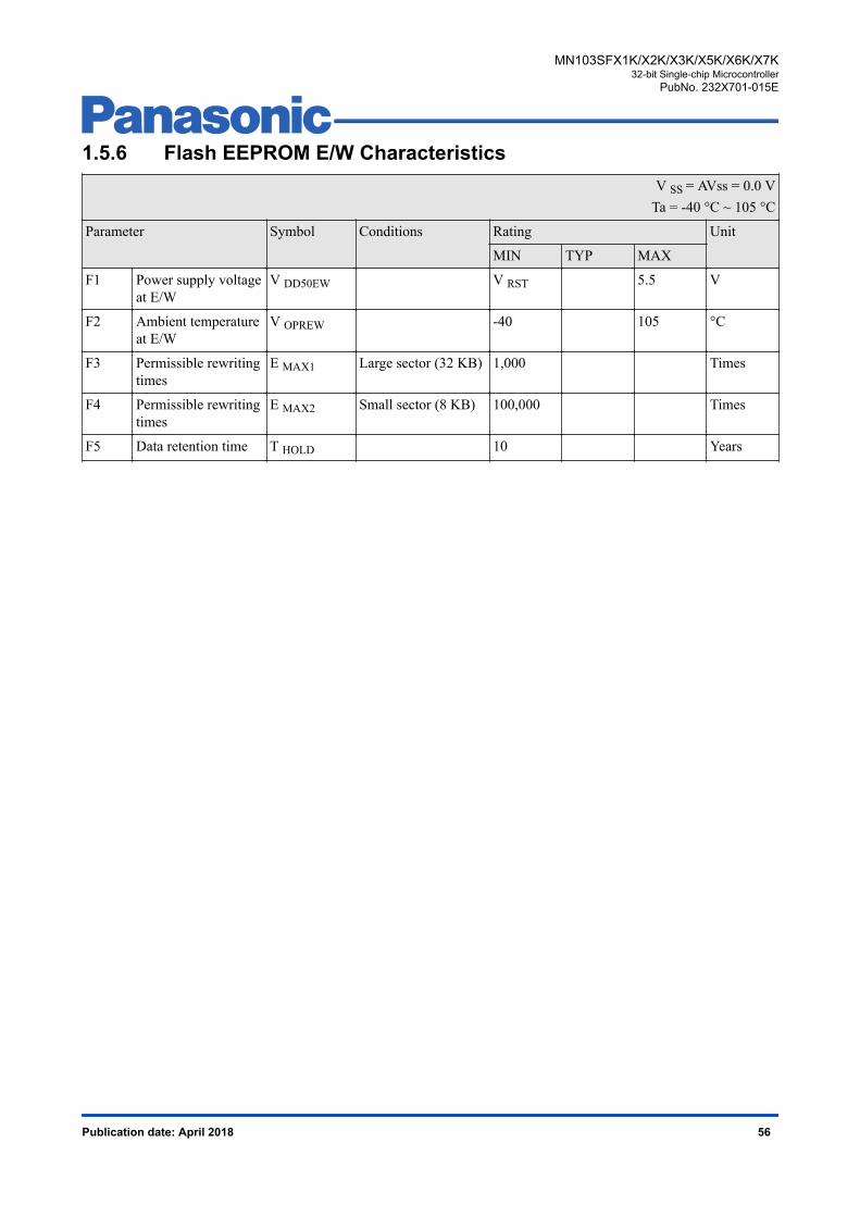
1.5.6 Flash EEPROM E/W CharacteristicsV SS = AVss = 0.0 V
Ta = -40 °C ~ 105 °C
Parameter Symbol Conditions Rating Unit
MIN TYP MAX
F1 Power supply voltageat E/W
V DD50EW V RST 5.5 V
F2 Ambient temperatureat E/W
V OPREW -40 105 °C
F3 Permissible rewritingtimes
E MAX1 Large sector (32 KB) 1,000 Times
F4 Permissible rewritingtimes
E MAX2 Small sector (8 KB) 100,000 Times
F5 Data retention time T HOLD 10 Years
MN103SFX1K/X2K/X3K/X5K/X6K/X7K32-bit Single-chip Microcontroller
PubNo. 232X701-015E
Publication date: April 2018 56
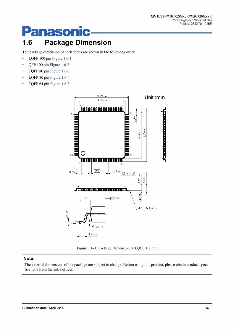
1.6 Package DimensionThe package dimension of each series are shown in the following order.• LQFP 100 pin Figure 1.6-1 • QFP 100 pin Figure 1.6-2 • TQFP 80 pin Figure 1.6-3 • LQFP 80 pin Figure 1.6-4 • TQFP 64 pin Figure 1.6-5
Figure 1.6-1 Package Dimension of LQFP 100 pin
Note:The external dimensions of the package are subject to change. Before using this product, please obtain product speci-fications from the sales offices.
MN103SFX1K/X2K/X3K/X5K/X6K/X7K32-bit Single-chip Microcontroller
PubNo. 232X701-015E
Publication date: April 2018 57

Unit :mm
Figure 1.6-2 Package Dimension of QFP 100 pin
Note:The external dimensions of the package are subject to change. Before using this product, please obtain product speci-fications from the sales offices.
MN103SFX1K/X2K/X3K/X5K/X6K/X7K32-bit Single-chip Microcontroller
PubNo. 232X701-015E
Publication date: April 2018 58

Figure 1.6-3 Package Dimension of TQFP 80 pin
Note:The external dimensions of the package are subject to change. Before using this product, please obtain product speci-fications from the sales offices.
MN103SFX1K/X2K/X3K/X5K/X6K/X7K32-bit Single-chip Microcontroller
PubNo. 232X701-015E
Publication date: April 2018 59

Figure 1.6-4 Package Dimension of LQFP 80 pin
Note:The external dimensions of the package are subject to change. Before using this product, please obtain product speci-fications from the sales offices.
MN103SFX1K/X2K/X3K/X5K/X6K/X7K32-bit Single-chip Microcontroller
PubNo. 232X701-015E
Publication date: April 2018 60

Figure 1.6-5 Package Dimension of TQFP 64 pin
Note:The external dimensions of the package are subject to change. Before using this product, please obtain product speci-fications from the sales offices.
MN103SFX1K/X2K/X3K/X5K/X6K/X7K32-bit Single-chip Microcontroller
PubNo. 232X701-015E
Publication date: April 2018 61
Request for your special attention and precautions in using the technical information andsemiconductors described in this book
(1) If any of the products or technical information described in this book is to be exported or provided to non-residents, the laws andregulations of the exporting country, especially, those with regard to security export control, must be observed.
(2) The technical information described in this book is intended only to show the main characteristics and application circuit examplesof the products. No license is granted in and to any intellectual property right or other right owned by Panasonic Corporation or anyother company. Therefore, no responsibility is assumed by our company as to the infringement upon any such right owned by anyother company which may arise as a result of the use of technical information described in this book.
(3) The products described in this book are intended to be used for general applications (such as office equipment, communicationsequipment, measuring instruments and household appliances), or for specific applications as expressly stated in this book.Consult our sales staff in advance for information on the following applications: Special applications (such as for airplanes, aerospace, automotive equipment, traffic signaling equipment, combustion equipment,
life support systems and safety devices) in which exceptional quality and reliability are required, or if the failure or malfunction ofthe products may directly jeopardize life or harm the human body.
It is to be understood that our company shall not be held responsible for any damage incurred as a result of or in connection withyour using the products described in this book for any special application, unless our company agrees to your using the products inthis book for any special application.
(4) The products and product specifications described in this book are subject to change without notice for modification and/or improve-ment. At the final stage of your design, purchasing, or use of the products, therefore, ask for the most up-to-date Product Standards in advance to make sure that the latest specifications satisfy your requirements.
(5) When designing your equipment, comply with the range of absolute maximum rating and the guaranteed operating conditions(operating power supply voltage and operating environment etc.). Especially, please be careful not to exceed the range of absolutemaximum rating on the transient state, such as power-on, power-off and mode-switching. Otherwise, we will not be liable for anydefect which may arise later in your equipment.Even when the products are used within the guaranteed values, take into the consideration of incidence of break down and failuremode, possible to occur to semiconductor products. Measures on the systems such as redundant design, arresting the spread of fire orpreventing glitch are recommended in order to prevent physical injury, fire, social damages, for example, by using the products.
(6) Comply with the instructions for use in order to prevent breakdown and characteristics change due to external factors (ESD, EOS,thermal stress and mechanical stress) at the time of handling, mounting or at customer's process. When using products for whichdamp-proof packing is required, satisfy the conditions, such as shelf life and the elapsed time since first opening the packages.
(7) This book may be not reprinted or reproduced whether wholly or partially, without the prior written permission of our company.
No.020210