is31fl3742 - issi · is31fl3742 integrated silicon solution, inc. – 3 rev. a, 12/13/2017 pin...
TRANSCRIPT

IS31FL3742
Integrated Silicon Solution, Inc. – www.issi.com 1 Rev. A, 12/13/2017
30×6 DOTS MATRIX LED DRIVER
December 2017
GENERAL DESCRIPTION
The IS31FL3742 is a general purpose 30×6 LED Matrix programmed via an I2C compatible interface. Each LED can be dimmed individually with 8-bit PWM data and 8-bit scaling data which allowing 256 steps of linear PWM dimming and 256 steps of DC current adjustable level.
Additionally each LED open and short state can be detected, IS31FL3742 store the open or short information in Open-Short Registers. The Open-Short Registers allowing MCU to read out via I2C compatible interface. Inform MCU whether there are LEDs open or short and the locations of open or short LEDs.
The IS31FL3742 operates from 2.7V to 5.5V and features a very low shutdown and operational current.
IS31FL3742 is available in QFN-48 (6mm×6mm) package. It operates from 2.7V to 5.5V over the temperature range of -40°C to +125°C.
FEATURES
Supply voltage range: 2.7V to 5.5V 30 Current Sink × 6 SW matrix size: drive up to
180 LEDs or 60 RGBs Individual 256 PWM control steps Individual 256 DC current steps Global 256 current setting SDB rising edge reset I2C module Programmable H/L logic: 1.4V/0.4V, 2.4V/0.6V 29kHz PWM frequency 1MHz I2C-compatible interface interrupt and state lookup registers Individual open and short error detect function De-ghost QFN-48 (6mm×6mm) package
APPLICATIONS
Mobile phones and other hand-held devices for LED display
Gaming device (Keyboard, mouse etc.) LED in write goods application Music box
TYPICAL APPLICATION CIRCUIT
Figure 1 Typical Application Circuit (Single Color: 30x6)
SDA
SCL
ADDR
IS31FL3742
1k1k
VIO/MCU
100k
INTB
100k
GND
SW1
SW2
CS30
CS29
CS2
CS1
SW5
SW6
SDB
Micro Controller
PVCC
AVCC
1 F
1 F
5V
PVCC
1 F 0.1 F
SW1 SW2 SW3
CS1
CS3
CS28
CS29
CS30
CS2
SW4 SW5 SW6
R_EXT
10k
0.1 F
0.1 F
12
19
11
6
7
4
8
10
5
120
21
2
3
13
14
17
18
9,30
0.1 F
20
20
20
20
20
20

IS31FL3742
Integrated Silicon Solution, Inc. – www.issi.com 2 Rev. A, 12/13/2017
TYPICAL APPLICATION CIRCUIT (CONTINUED)
Figure 2 Typical Application Circuit (RGB Color: 10x6)
Note: For the mobile applications the IC should be placed far away from the mobile antenna in order to prevent the EMI.
SW1 SW2 SW3 SW4 SW5 SW6
SDA
SCL
ADDR
IS31FL3742
1k1k
VIO/MCU
100k
INTB
100k
GND
SW1
SW2
CS30
CS29
CS2
CS1
SW5
SW6
SDB
Micro Controller
PVCC
AVCC
1 F
1 F
5V
PVCC
1 F 0.1 F
R_EXT
10k
0.1 F
0.1 F
12
19
11
6
7
4
8
10
5
120
21
2
3
13
14
17
18
9,30
CS1
CS3
CS28
CS29
CS30
CS2
20R
51R
20R
20R
51R
20R0.1 F
IS31FL3742
Integrated Silicon Solution, Inc. – www.issi.com 3 Rev. A, 12/13/2017
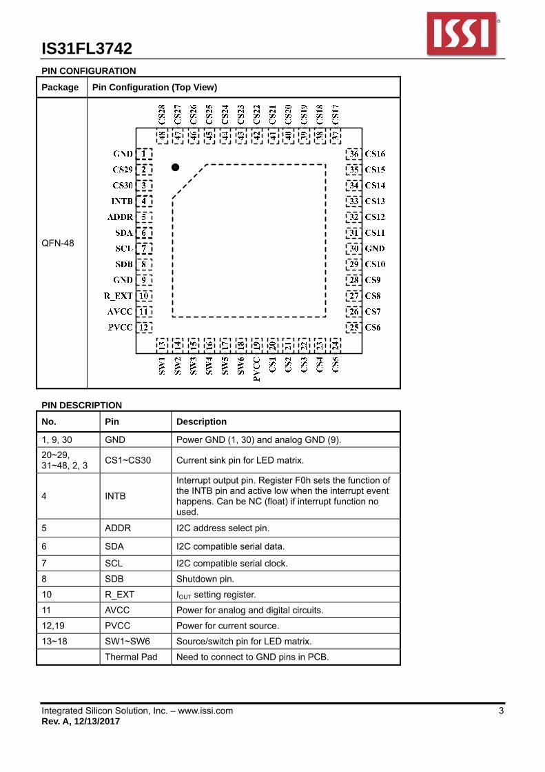
PIN CONFIGURATION
Package Pin Configuration (Top View)
QFN-48
PIN DESCRIPTION
No. Pin Description
1, 9, 30 GND Power GND (1, 30) and analog GND (9).
20~29, 31~48, 2, 3
CS1~CS30 Current sink pin for LED matrix.
4 INTB
Interrupt output pin. Register F0h sets the function of the INTB pin and active low when the interrupt event happens. Can be NC (float) if interrupt function no used.
5 ADDR I2C address select pin.
6 SDA I2C compatible serial data.
7 SCL I2C compatible serial clock.
8 SDB Shutdown pin.
10 R_EXT IOUT setting register.
11 AVCC Power for analog and digital circuits.
12,19 PVCC Power for current source.
13~18 SW1~SW6 Source/switch pin for LED matrix.
Thermal Pad Need to connect to GND pins in PCB.
IS31FL3742
Integrated Silicon Solution, Inc. – www.issi.com 4 Rev. A, 12/13/2017
ORDERING INFORMATION Industrial Range: -40°C to +125°C
Order Part No. Package QTY/Reel
IS31FL3742-QFLS4-TR QFN-48, Lead-free 2500
Copyright © 2017 Integrated Silicon Solution, Inc. All rights reserved. ISSI reserves the right to make changes to this specification and its products at any time without notice. ISSI assumes no liability arising out of the application or use of any information, products or services described herein. Customers are advised to obtain the latest version of this device specification before relying on any published information and before placing orders for products. Integrated Silicon Solution, Inc. does not recommend the use of any of its products in life support applications where the failure or malfunction of the product can reasonably be expected to cause failure of the life support system or to significantly affect its safety or effectiveness. Products are not authorized for use in such applications unless Integrated Silicon Solution, Inc. receives written assurance to its satisfaction, that: a.) the risk of injury or damage has been minimized; b.) the user assume all such risks; and c.) potential liability of Integrated Silicon Solution, Inc is adequately protected under the circumstances
IS31FL3742
Integrated Silicon Solution, Inc. – www.issi.com 5 Rev. A, 12/13/2017
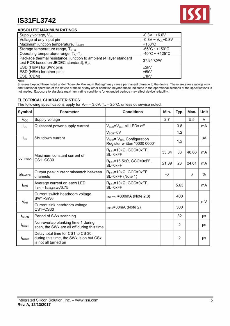
ABSOLUTE MAXIMUM RATINGS Supply voltage, VCC -0.3V ~+6.0V Voltage at any input pin -0.3V ~ VCC+0.3V Maximum junction temperature, TJMAX +150°C Storage temperature range, TSTG -65°C ~+150°C Operating temperature range, TA=TJ -40°C ~ +125°C Package thermal resistance, junction to ambient (4 layer standard test PCB based on JEDEC standard), θJA
37.84°C/W
ESD (HBM) for SWx pins ESD (HBM) for other pins ESD (CDM)
±2kV ±5kV ±1kV
Note: Stresses beyond those listed under “Absolute Maximum Ratings” may cause permanent damage to the device. These are stress ratings only and functional operation of the device at these or any other condition beyond those indicated in the operational sections of the specifications is not implied. Exposure to absolute maximum rating conditions for extended periods may affect device reliability. ELECTRICAL CHARACTERISTICS The following specifications apply for VCC = 3.6V, TA = 25°C, unless otherwise noted.
Symbol Parameter Conditions Min. Typ. Max. Unit
VCC Supply voltage 2.7 5.5 V
ICC Quiescent power supply current VSDB=VCC, all LEDs off 3.8 mA
ISD Shutdown current
VSDB=0V 1.2
μA VSDB= VCC, Configuration Register written “0000 0000”
1.2
IOUT(PEAK) Maximum constant current of CS1~CS30
REXT=10kΩ, GCC=0xFF, SL=0xFF
35.34 38 40.66 mA
REXT=16.5kΩ, GCC=0xFF, SL=0xFF
21.39 23 24.61 mA
∆IMATCH Output peak current mismatch between channels
REXT=10kΩ, GCC=0xFF, SL=0xFF (Note 1)
-6 6 %
ILED Average current on each LED ILED = IOUT(PEAK)/6.75
REXT=10kΩ, GCC=0xFF, SL=0xFF
5.63 mA
VHR
Current switch headroom voltage SW1~SW6
ISWITCH=800mA (Note 2,3) 400
mV Current sink headroom voltage CS1~CS30
ISINK=38mA (Note 2) 300
tSCAN Period of SWx scanning 32 µs
tNOL1 Non-overlap blanking time 1 during scan, the SWx are all off during this time
2 µs
tNOL2 Delay total time for CS1 to CS 30, during this time, the SWx is on but CSx is not all turned on
2 µs
IS31FL3742
Integrated Silicon Solution, Inc. – www.issi.com 6 Rev. A, 12/13/2017
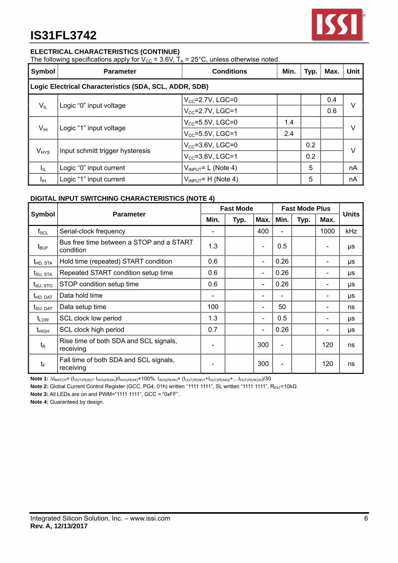
ELECTRICAL CHARACTERISTICS (CONTINUE) The following specifications apply for VCC = 3.6V, TA = 25°C, unless otherwise noted.
Symbol Parameter Conditions Min. Typ. Max. Unit
Logic Electrical Characteristics (SDA, SCL, ADDR, SDB)
VIL Logic “0” input voltage VCC=2.7V, LGC=0 0.4
V VCC=2.7V, LGC=1 0.6
VIH Logic “1” input voltage VCC=5.5V, LGC=0 1.4
V VCC=5.5V, LGC=1 2.4
VHYS Input schmitt trigger hysteresis VCC=3.6V, LGC=0 0.2
V VCC=3.6V, LGC=1 0.2
IIL Logic “0” input current VINPUT= L (Note 4) 5 nA
IIH Logic “1” input current VINPUT= H (Note 4) 5 nA
DIGITAL INPUT SWITCHING CHARACTERISTICS (NOTE 4)
Symbol Parameter Fast Mode Fast Mode Plus
UnitsMin. Typ. Max. Min. Typ. Max.
fSCL Serial-clock frequency - 400 - 1000 kHz
tBUF Bus free time between a STOP and a START condition
1.3 - 0.5 - μs
tHD, STA Hold time (repeated) START condition 0.6 - 0.26 - μs
tSU, STA Repeated START condition setup time 0.6 - 0.26 - μs
tSU, STO STOP condition setup time 0.6 - 0.26 - μs
tHD, DAT Data hold time - - - - μs
tSU, DAT Data setup time 100 - 50 - ns
tLOW SCL clock low period 1.3 - 0.5 - μs
tHIGH SCL clock high period 0.7 - 0.26 - μs
tR Rise time of both SDA and SCL signals, receiving
- 300 - 120 ns
tF Fall time of both SDA and SCL signals, receiving
- 300 - 120 ns
Note 1: ∆IMATCH= (IOUT(PEAK)- IAVG(PEAK))/IAVG(PEAK)×100%. IAVG(PEAK)= (IOUT(PEAK)1+IOUT(PEAK)2+…IOUT(PEAK)30)/30
Note 2: Global Current Control Register (GCC, PG4, 01h) written “1111 1111”, SL written “1111 1111”, REXT=10kΩ.
Note 3: All LEDs are on and PWM=“1111 1111”, GCC = “0xFF”.
Note 4: Guaranteed by design.
IS31FL3742
Integrated Silicon Solution, Inc. – www.issi.com 7 Rev. A, 12/13/2017
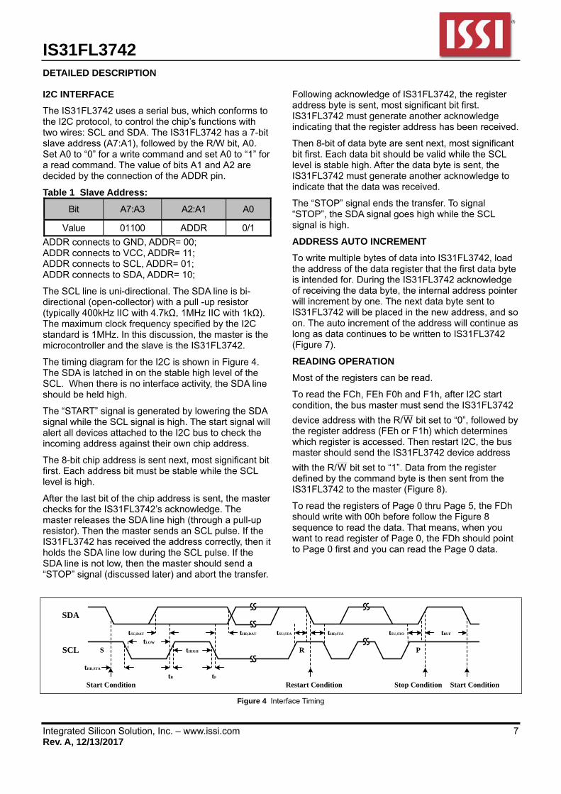
DETAILED DESCRIPTION I2C INTERFACE
The IS31FL3742 uses a serial bus, which conforms to the I2C protocol, to control the chip’s functions with two wires: SCL and SDA. The IS31FL3742 has a 7-bit slave address (A7:A1), followed by the R/W bit, A0. Set A0 to “0” for a write command and set A0 to “1” for a read command. The value of bits A1 and A2 are decided by the connection of the ADDR pin.
Table 1 Slave Address:
Bit A7:A3 A2:A1 A0
Value 01100 ADDR 0/1
ADDR connects to GND, ADDR= 00; ADDR connects to VCC, ADDR= 11; ADDR connects to SCL, ADDR= 01; ADDR connects to SDA, ADDR= 10;
The SCL line is uni-directional. The SDA line is bi-directional (open-collector) with a pull -up resistor (typically 400kHz IIC with 4.7kΩ, 1MHz IIC with 1kΩ). The maximum clock frequency specified by the I2C standard is 1MHz. In this discussion, the master is the microcontroller and the slave is the IS31FL3742.
The timing diagram for the I2C is shown in Figure 4. The SDA is latched in on the stable high level of the SCL. When there is no interface activity, the SDA line should be held high.
The “START” signal is generated by lowering the SDA signal while the SCL signal is high. The start signal will alert all devices attached to the I2C bus to check the incoming address against their own chip address.
The 8-bit chip address is sent next, most significant bit first. Each address bit must be stable while the SCL level is high.
After the last bit of the chip address is sent, the master checks for the IS31FL3742’s acknowledge. The master releases the SDA line high (through a pull-up resistor). Then the master sends an SCL pulse. If the IS31FL3742 has received the address correctly, then it holds the SDA line low during the SCL pulse. If the SDA line is not low, then the master should send a “STOP” signal (discussed later) and abort the transfer.
Following acknowledge of IS31FL3742, the register address byte is sent, most significant bit first. IS31FL3742 must generate another acknowledge indicating that the register address has been received.
Then 8-bit of data byte are sent next, most significant bit first. Each data bit should be valid while the SCL level is stable high. After the data byte is sent, the IS31FL3742 must generate another acknowledge to indicate that the data was received.
The “STOP” signal ends the transfer. To signal “STOP”, the SDA signal goes high while the SCL signal is high.
ADDRESS AUTO INCREMENT
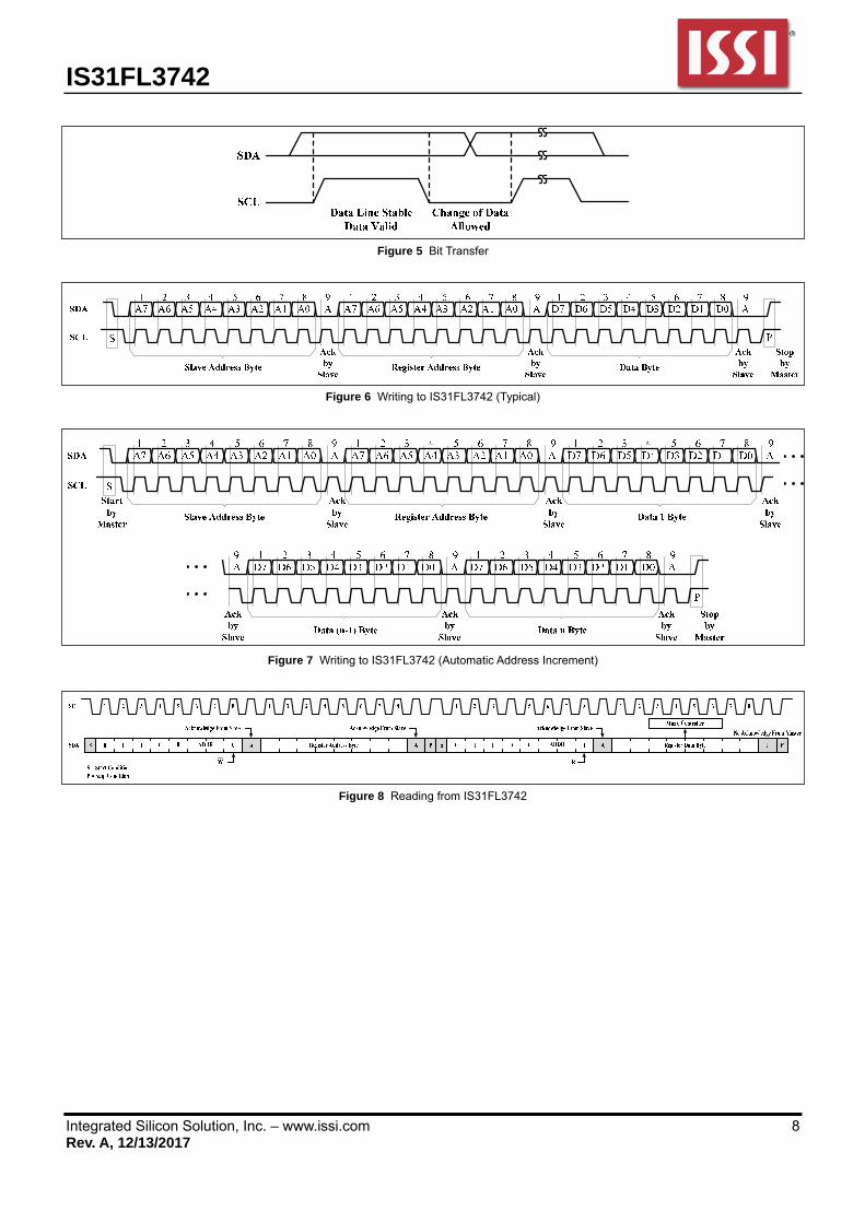
To write multiple bytes of data into IS31FL3742, load the address of the data register that the first data byte is intended for. During the IS31FL3742 acknowledge of receiving the data byte, the internal address pointer will increment by one. The next data byte sent to IS31FL3742 will be placed in the new address, and so on. The auto increment of the address will continue as long as data continues to be written to IS31FL3742 (Figure 7).
READING OPERATION
Most of the registers can be read.
To read the FCh, FEh F0h and F1h, after I2C start condition, the bus master must send the IS31FL3742
device address with the R/W____
bit set to “0”, followed by the register address (FEh or F1h) which determines which register is accessed. Then restart I2C, the bus master should send the IS31FL3742 device address
with the R/W____
bit set to “1”. Data from the register defined by the command byte is then sent from the IS31FL3742 to the master (Figure 8).
To read the registers of Page 0 thru Page 5, the FDh should write with 00h before follow the Figure 8 sequence to read the data. That means, when you want to read register of Page 0, the FDh should point to Page 0 first and you can read the Page 0 data.
Figure 4 Interface Timing
SDA
SCL
tHD,STA
tLOW
tHIGH
tSU,DAT tHD,DAT
tR tF
tSU,STA tHD,STA tSU,STO tBUF
S R P
Start Condition Restart Condition Stop Condition Start Condition
IS31FL3742
Integrated Silicon Solution, Inc. – www.issi.com 8 Rev. A, 12/13/2017
Figure 5 Bit Transfer
Figure 6 Writing to IS31FL3742 (Typical)
Figure 7 Writing to IS31FL3742 (Automatic Address Increment)
Figure 8 Reading from IS31FL3742
IS31FL3742
Integrated Silicon Solution, Inc. – www.issi.com 9 Rev. A, 12/13/2017
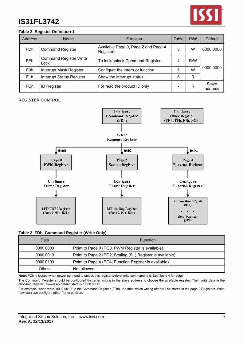
Table 2 Register Definition-1
Address Name Function Table R/W Default
FDh Command Register Available Page 0, Page 2 and Page 4 Registers
3 W 0000 0000
FEh Command Register Write Lock
To lock/unlock Command Register 4 R/W
0000 0000F0h Interrupt Mask Register Configure the interrupt function 5 W
F1h Interrupt Status Register Show the interrupt status 6 R
FCh ID Register For read the product ID only - R Slave
address
REGISTER CONTROL
Table 3 FDh Command Register (Write Only)
Data Function
0000 0000 Point to Page 0 (PG0, PWM Register is available)
0000 0010 Point to Page 2 (PG2, Scaling (SL) Register is available)
0000 0100 Point to Page 4 (PG4, Function Register is available)
Others Not allowed
Note: FDh is locked when power up, need to unlock this register before write command to it. See Table 4 for detail.
The Command Register should be configured first after writing in the slave address to choose the available register. Then write data in the choosing register. Power up default state is “0000 0000”.
For example, when write “0000 0010” in the Command Register (FDh), the data which writing after will be stored in the page 2 Registers. Write new data can configure other frame position.
IS31FL3742
Integrated Silicon Solution, Inc. – www.issi.com 10 Rev. A, 12/13/2017
Table 4 FEh Command Register Write Lock (Read/Write)
Bit D7:D0
Name CRWL
Default 0000 0000
To select the PG0, PG2 and PG4, need to unlock this register first, with the purpose to avoid mis-operation of this register. When FEh is written with 0xC5, FDh is allowed to modify once, after the FDh is modified the FEh will reset to be 0x00 at once. CRWL Command Register Write Lock 0000 0000 FDh write disable 1100 0101 FDh write enable once Table 5 F0h Interrupt Mask Register
Bit D7:D5 D4 D3:D2 D1 D0
Name - IAC - IS IO
Default 000 0 00 0 0
Configure the interrupt function for IC.
IAC Auto Clear Interrupt Bit 0 Interrupt could not auto clear 1 Interrupt auto clear when INTB stay low exceeds 8ms IS Dot Short Interrupt Bit 0 Disable dot short interrupt 1 Enable dot short interrupt IO Dot Open Interrupt Bit 0 Disable dot open interrupt 1 Enable dot open interrupt
Table 6 F1h Interrupt Status Register (Read Only)
Bit D7:D2 D1 D0
Name - SB OB
Default 0000 00 0 0
Show the interrupt status for IC. SB Short Bit 0 No short 1 Short happens OB Open Bit 0 No open 1 Open happens FCh ID Register ID register is read only and read result is the device slave address. For example, if ADDR pin connects to GND, read result is 0x60.
IS31FL3742
Integrated Silicon Solution, Inc. – www.issi.com 11 Rev. A, 12/13/2017
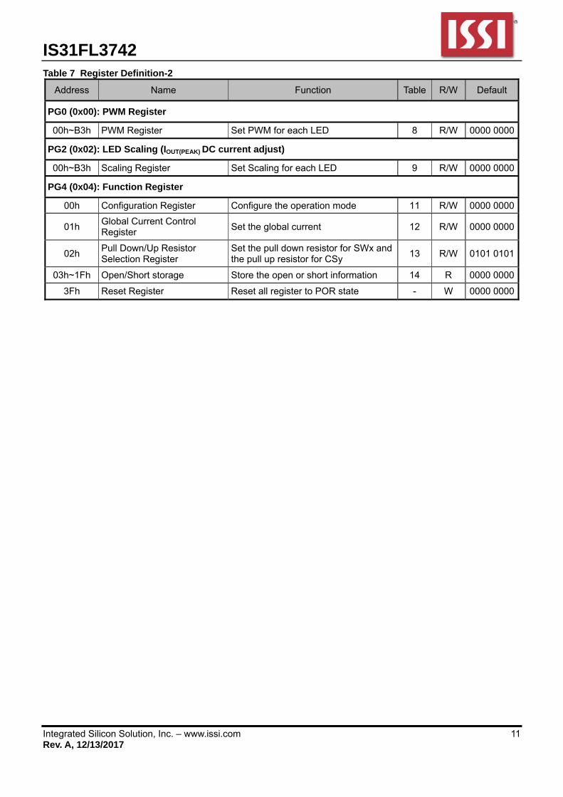
Table 7 Register Definition-2
Address Name Function Table R/W Default
PG0 (0x00): PWM Register
00h~B3h PWM Register Set PWM for each LED 8 R/W 0000 0000
PG2 (0x02): LED Scaling (IOUT(PEAK) DC current adjust)
00h~B3h Scaling Register Set Scaling for each LED 9 R/W 0000 0000
PG4 (0x04): Function Register
00h Configuration Register Configure the operation mode 11 R/W 0000 0000
01h Global Current Control Register
Set the global current 12 R/W 0000 0000
02h Pull Down/Up Resistor Selection Register
Set the pull down resistor for SWx and the pull up resistor for CSy
13 R/W 0101 0101
03h~1Fh Open/Short storage Store the open or short information 14 R 0000 0000
3Fh Reset Register Reset all register to POR state - W 0000 0000
IS31FL3742
Integrated Silicon Solution, Inc. – www.issi.com 12 Rev. A, 12/13/2017
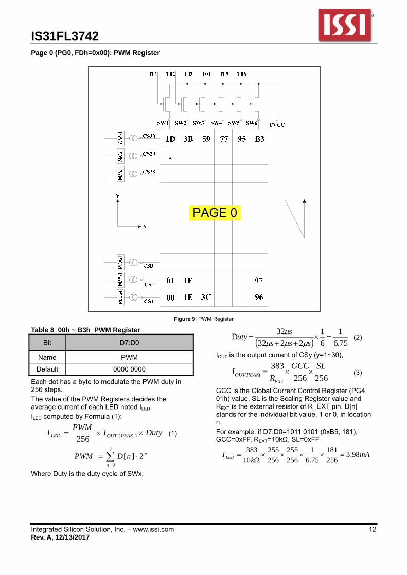
Page 0 (PG0, FDh=0x00): PWM Register
Figure 9 PWM Register
Table 8 00h ~ B3h PWM Register
Bit D7:D0
Name PWM
Default 0000 0000
Each dot has a byte to modulate the PWM duty in 256 steps. The value of the PWM Registers decides the average current of each LED noted ILED. ILED computed by Formula (1):
DutyIPWM
I PEAKOUTLED )(256 (1)
7
0
2][n
nnDPWM
Where Duty is the duty cycle of SWx,
75.6
1
6
1
2232
32D
sss
suty
(2)
IOUT is the output current of CSy (y=1~30),
256256
383)(
SLGCC
RI
EXTPEAKOUT
(3)
GCC is the Global Current Control Register (PG4, 01h) value, SL is the Scaling Register value and REXT is the external resistor of R_EXT pin. D[n] stands for the individual bit value, 1 or 0, in location n. For example: if D7:D0=1011 0101 (0xB5, 181), GCC=0xFF, REXT=10kΩ, SL=0xFF
mAk
I LED 98.3256
181
75.6
1
256
255
256
255
10
383
IS31FL3742
Integrated Silicon Solution, Inc. – www.issi.com 13 Rev. A, 12/13/2017
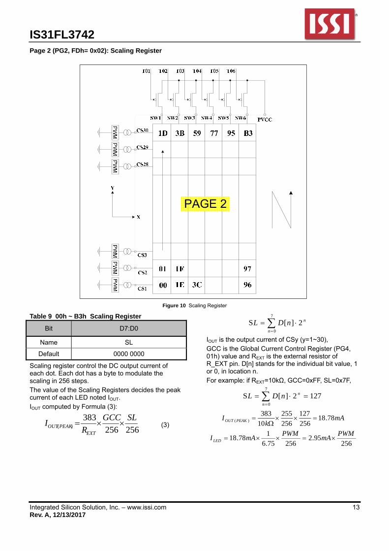
Page 2 (PG2, FDh= 0x02): Scaling Register
Figure 10 Scaling Register
Table 9 00h ~ B3h Scaling Register
Bit D7:D0
Name SL
Default 0000 0000
Scaling register control the DC output current of each dot. Each dot has a byte to modulate the scaling in 256 steps. The value of the Scaling Registers decides the peak current of each LED noted IOUT. IOUT computed by Formula (3):
256256
383)(
SLGCC
RI
EXTPEAKOUT (3)
7
0
2][Sn
nnDL
IOUT is the output current of CSy (y=1~30), GCC is the Global Current Control Register (PG4, 01h) value and REXT is the external resistor of R_EXT pin. D[n] stands for the individual bit value, 1 or 0, in location n. For example: if REXT=10kΩ, GCC=0xFF, SL=0x7F,
1272][S7
0
n
nnDL
mAk
I PEAKOUT 78.18256
127
256
255
10
383)(
25695.2
25675.6
178.18
PWMmA
PWMmAILED
IS31FL3742
Integrated Silicon Solution, Inc. – www.issi.com 14 Rev. A, 12/13/2017
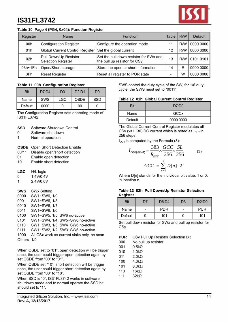
Table 10 Page 4 (PG4, 0x04): Function Register
Register Name Function Table R/W Default
00h Configuration Register Configure the operation mode 11 R/W 0000 0000
01h Global Current Control Register Set the global current 12 R/W 0000 0000
02h Pull Down/Up Resistor Selection Register
Set the pull down resistor for SWx and the pull up resistor for CSy
13 R/W 0101 0101
03h~1Fh Open/Short storage Store the open or short information 14 R 0000 0000
3Fh Reset Register Reset all register to POR state - W 0000 0000
Table 11 00h Configuration Register
Bit D7:D4 D3 D2:D1 D0
Name SWS LGC OSDE SSD
Default 0000 0 00 0
The Configuration Register sets operating mode of IS31FL3742. SSD Software Shutdown Control 0 Software shutdown 1 Normal operation OSDE Open Short Detection Enable 00/11 Disable open/short detection 01 Enable open detection 10 Enable short detection LGC H/L logic 0 1.4V/0.4V 1 2.4V/0.6V SWS SWx Setting 0000 SW1~SW6, 1/9 0001 SW1~SW6, 1/8 0010 SW1~SW6, 1/7 0011 SW1~SW6, 1/6 0100 SW1~SW5, 1/5, SW6 no-active 0101 SW1~SW4, 1/4, SW5~SW6 no-active 0110 SW1~SW3, 1/3, SW4~SW6 no-active 0111 SW1~SW2, 1/2, SW3~SW6 no-active 1000 All CSx work as current sinks only, no scan Others 1/9 When OSDE set to “01”, open detection will be trigger once, the user could trigger open detection again by set OSDE from “00” to “01”. When OSDE set “10”, short detection will be trigger once, the user could trigger short detection again by set OSDE from “00” to “10”. When SSD is “0”, IS31FL3742 works in software shutdown mode and to normal operate the SSD bit should set to “1”.
SWS control the duty cycle of the SW, for 1/6 duty cycle, the SWS must set to “0011”. Table 12 01h Global Current Control Register
Bit D7:D0
Name GCCx
Default 0000 0000
The Global Current Control Register modulates all CSy (x=1~30) DC current which is noted as IOUT in 256 steps. IOUT is computed by the Formula (3):
256256
383)(
SLGCC
RI
EXTPEAKOUT (3)
7
0
2][n
nnDGCC
Where D[n] stands for the individual bit value, 1 or 0, in location n.
Table 13 02h Pull Down/Up Resistor Selection Register
Bit D7 D6:D4 D3 D2:D0
Name - PDR - PUR
Default 0 101 0 101
Set pull down resistor for SWx and pull up resistor for CSy.
PUR CSy Pull Up Resistor Selection Bit 000 No pull up resistor 001 0.5kΩ 010 1.0kΩ 011 2.0kΩ 100 4.0kΩ 101 8.0kΩ 110 16kΩ 111 32kΩ
IS31FL3742
Integrated Silicon Solution, Inc. – www.issi.com 15 Rev. A, 12/13/2017
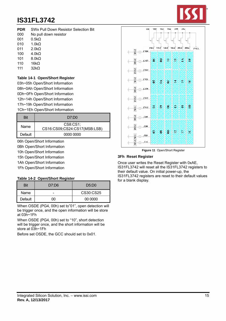
PDR SWx Pull Down Resistor Selection Bit 000 No pull down resistor 001 0.5kΩ 010 1.0kΩ 011 2.0kΩ 100 4.0kΩ 101 8.0kΩ 110 16kΩ 111 32kΩ Table 14-1 Open/Short Register 03h~05h Open/Short Information 08h~0Ah Open/Short Information 0Dh~0Fh Open/Short Information 12h~14h Open/Short Information 17h~19h Open/Short Information 1Ch~1Eh Open/Short Information
Bit D7:D0
Name CS8:CS1;
CS16:CS09;CS24:CS17(MSB:LSB)
Default 0000 0000
06h Open/Short Information 0Bh Open/Short Information 10h Open/Short Information 15h Open/Short Information 1Ah Open/Short Information 1Fh Open/Short Information
Table 14-2 Open/Short Register
Bit D7:D6 D5:D0
Name - CS30:CS25
Default 00 00 0000
When OSDE (PG4, 00h) set to”01”, open detection will be trigger once, and the open information will be store at 03h~1Fh When OSDE (PG4, 00h) set to “10”, short detection will be trigger once, and the short information will be store at 03h~1Fh Before set OSDE, the GCC should set to 0x01.
Figure 11 Open/Short Register
3Fh Reset Register
Once user writes the Reset Register with 0xAE, IS31FL3742 will reset all the IS31FL3742 registers to their default value. On initial power-up, the IS31FL3742 registers are reset to their default values for a blank display.
IS31FL3742
Integrated Silicon Solution, Inc. – www.issi.com 16 Rev. A, 12/13/2017
APPLICATION INFORMATION
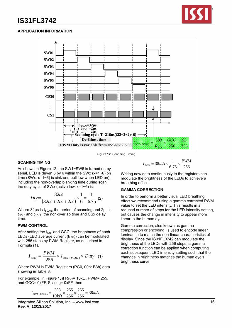
Figure 12 Scanning Timing
SCANING TIMING
As shown in Figure 12, the SW1~SW6 is turned on by serial, LED is driven 6 by 6 within the SWx (x=1~6) on time (SWx, x=1~6) is sink and pull low when LED on) , including the non-overlap blanking time during scan, the duty cycle of SWx (active low, x=1~6) is:
75.6
1
6
1
2232
32D
sss
suty
(2)
Where 32μs is tSCAN, the period of scanning and 2μs is tNOL1 and tNOL2, the non-overlap time and CSx delay time.
PWM CONTROL
After setting the IOUT and GCC, the brightness of each LEDs (LED average current (ILED)) can be modulated with 256 steps by PWM Register, as described in Formula (1).
DutyIPWM
I PEAKOUTLED )(256 (1)
Where PWM is PWM Registers (PG0, 00h~B3h) data showing in Table 8.
For example, in Figure 1, if REXT= 10kΩ, PWM= 255, and GCC= 0xFF, Scaling= 0xFF, then
mAk
I PEAKOUT 38256
255
256
255
10
383)(
25675.6
138
PWMmAI LED
Writing new data continuously to the registers can modulate the brightness of the LEDs to achieve a breathing effect.
GAMMA CORRECTION
In order to perform a better visual LED breathing effect we recommend using a gamma corrected PWM value to set the LED intensity. This results in a reduced number of steps for the LED intensity setting, but causes the change in intensity to appear more linear to the human eye.
Gamma correction, also known as gamma compression or encoding, is used to encode linear luminance to match the non-linear characteristics of display. Since the IS31FL3742 can modulate the brightness of the LEDs with 256 steps, a gamma correction function can be applied when computing each subsequent LED intensity setting such that the changes in brightness matches the human eye's brightness curve.
SW01
SW02
tNOL1=2µs
SW03
SW04
SW05
SW06
CS30
CS1
tSCAN=32µs
Scanning cycle T=216us((32+2+2)×6)
PWM Duty is variable from 0/256~255/256
De-Ghost time
256256
338)(
SLGCC
RI
EXTPEAKOUT
tNOL2=2µs
IS31FL3742
Integrated Silicon Solution, Inc. – www.issi.com 17 Rev. A, 12/13/2017
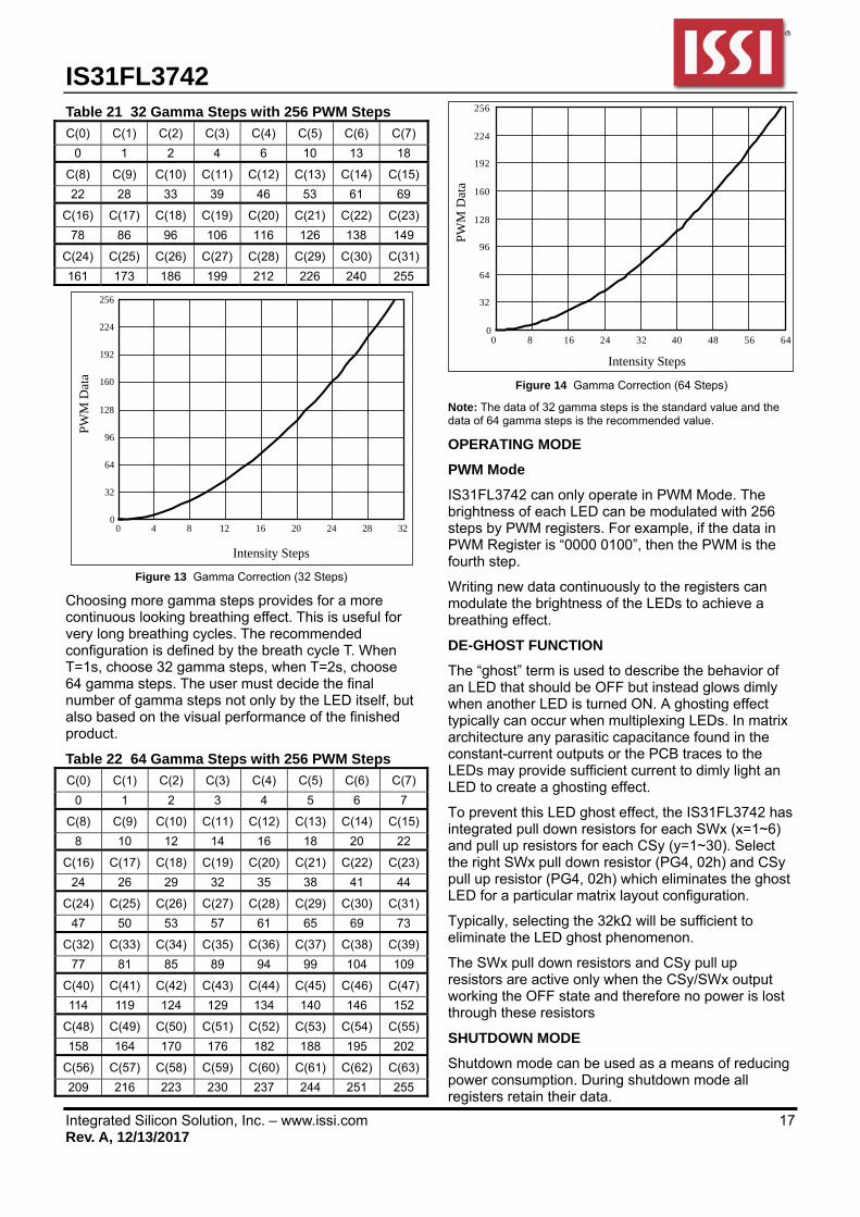
Table 21 32 Gamma Steps with 256 PWM Steps
C(0) C(1) C(2) C(3) C(4) C(5) C(6) C(7)
0 1 2 4 6 10 13 18
C(8) C(9) C(10) C(11) C(12) C(13) C(14) C(15)
22 28 33 39 46 53 61 69
C(16) C(17) C(18) C(19) C(20) C(21) C(22) C(23)
78 86 96 106 116 126 138 149
C(24) C(25) C(26) C(27) C(28) C(29) C(30) C(31)
161 173 186 199 212 226 240 255
Figure 13 Gamma Correction (32 Steps)
Choosing more gamma steps provides for a more continuous looking breathing effect. This is useful for very long breathing cycles. The recommended configuration is defined by the breath cycle T. When T=1s, choose 32 gamma steps, when T=2s, choose 64 gamma steps. The user must decide the final number of gamma steps not only by the LED itself, but also based on the visual performance of the finished product.
Table 22 64 Gamma Steps with 256 PWM Steps
C(0) C(1) C(2) C(3) C(4) C(5) C(6) C(7)
0 1 2 3 4 5 6 7
C(8) C(9) C(10) C(11) C(12) C(13) C(14) C(15)
8 10 12 14 16 18 20 22
C(16) C(17) C(18) C(19) C(20) C(21) C(22) C(23)
24 26 29 32 35 38 41 44
C(24) C(25) C(26) C(27) C(28) C(29) C(30) C(31)
47 50 53 57 61 65 69 73
C(32) C(33) C(34) C(35) C(36) C(37) C(38) C(39)
77 81 85 89 94 99 104 109
C(40) C(41) C(42) C(43) C(44) C(45) C(46) C(47)
114 119 124 129 134 140 146 152
C(48) C(49) C(50) C(51) C(52) C(53) C(54) C(55)
158 164 170 176 182 188 195 202
C(56) C(57) C(58) C(59) C(60) C(61) C(62) C(63)
209 216 223 230 237 244 251 255
Figure 14 Gamma Correction (64 Steps)
Note: The data of 32 gamma steps is the standard value and the data of 64 gamma steps is the recommended value.
OPERATING MODE
PWM Mode
IS31FL3742 can only operate in PWM Mode. The brightness of each LED can be modulated with 256 steps by PWM registers. For example, if the data in PWM Register is “0000 0100”, then the PWM is the fourth step.
Writing new data continuously to the registers can modulate the brightness of the LEDs to achieve a breathing effect.
DE-GHOST FUNCTION
The “ghost” term is used to describe the behavior of an LED that should be OFF but instead glows dimly when another LED is turned ON. A ghosting effect typically can occur when multiplexing LEDs. In matrix architecture any parasitic capacitance found in the constant-current outputs or the PCB traces to the LEDs may provide sufficient current to dimly light an LED to create a ghosting effect.
To prevent this LED ghost effect, the IS31FL3742 has integrated pull down resistors for each SWx (x=1~6) and pull up resistors for each CSy (y=1~30). Select the right SWx pull down resistor (PG4, 02h) and CSy pull up resistor (PG4, 02h) which eliminates the ghost LED for a particular matrix layout configuration.
Typically, selecting the 32kΩ will be sufficient to eliminate the LED ghost phenomenon.
The SWx pull down resistors and CSy pull up resistors are active only when the CSy/SWx output working the OFF state and therefore no power is lost through these resistors
SHUTDOWN MODE
Shutdown mode can be used as a means of reducing power consumption. During shutdown mode all registers retain their data.
0
32
64
96
128
160
192
224
256
0 4 8 12 16 20 24 28 32
PW
M D
ata
Intensity Steps
0
32
64
96
128
160
192
224
256
0 8 16 24 32 40 48 56 64
PW
M D
ata
Intensity Steps
IS31FL3742
Integrated Silicon Solution, Inc. – www.issi.com 18 Rev. A, 12/13/2017
Software Shutdown
By setting SSD bit of the Configuration Register (PG4, 00h) to “0”, the IS31FL3742 will operate in software shutdown mode. When the IS31FL3742 is in software shutdown, all current sources are switched off, so that the matrix is blanked. All registers can be operated. Typical current consume is 2μA.
Hardware Shutdown
The chip enters hardware shutdown when the SDB pin is pulled low. All analog circuits are disabled during hardware shutdown, typical the current consume is 2μA.
The chip releases hardware shutdown when the SDB pin is pulled high. When set SDB high, the rising edge will reset the I2C module, but the register information retains. During hardware shutdown state Function Register can be operated.
If VCC has risk drop below 1.75V but above 0.1V during SDB pulled low, please re-initialize all Function Registers before SDB pulled high.
LAYOUT
As described in external resistor (REXT), the chip consumes lots of power. Please consider below factors when layout the PCB.
1. The VCC (PVCC, AVCC) capacitors need to close to the chip and the ground side should well connect to the GND of the chip.
2. REXT should be close to the chip and the ground side should well connect to the GND of the chip.
3. The thermal pad should connect to ground pins and the PCB should have the thermal pad too, usually this pad should have 16 or 25 via thru the PCB to other side’s ground area to help radiate the heat. About the thermal pad size, please refer to the land pattern of each package.
4. The CSy pins maximum current is 38mA (REXT=10kΩ), and the SWx pins maximum current is larger, the width of the trace, SWx should have wider trace then CSy.
IS31FL3742
Integrated Silicon Solution, Inc. – www.issi.com 19 Rev. A, 12/13/2017
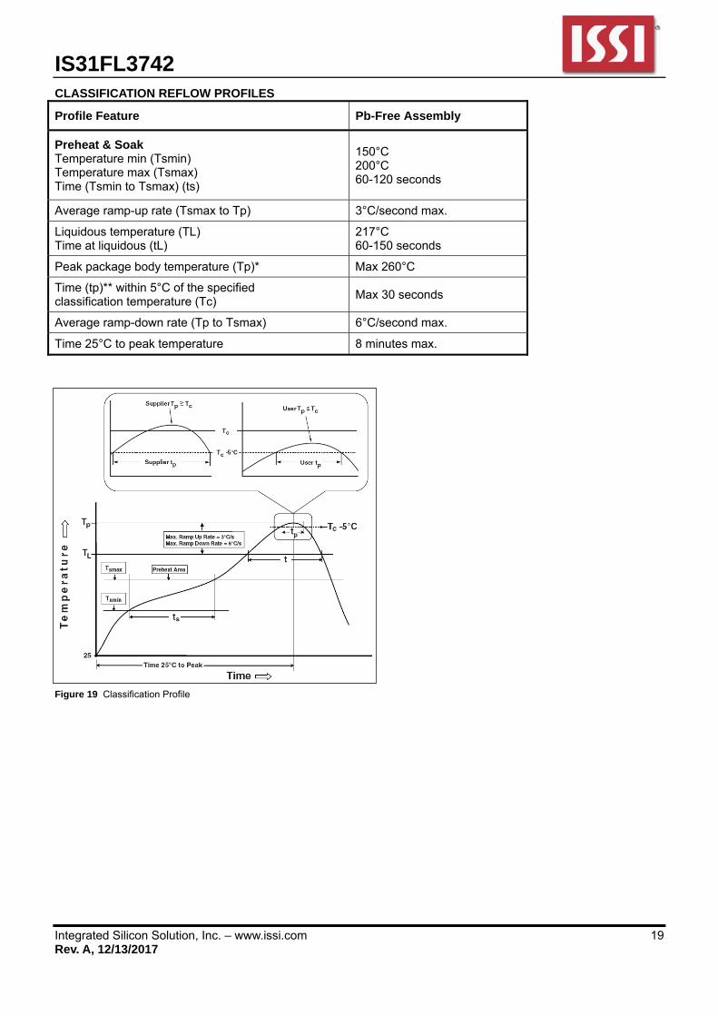
CLASSIFICATION REFLOW PROFILES
Profile Feature Pb-Free Assembly
Preheat & Soak Temperature min (Tsmin) Temperature max (Tsmax) Time (Tsmin to Tsmax) (ts)
150°C 200°C 60-120 seconds
Average ramp-up rate (Tsmax to Tp) 3°C/second max.
Liquidous temperature (TL) Time at liquidous (tL)
217°C 60-150 seconds
Peak package body temperature (Tp)* Max 260°C
Time (tp)** within 5°C of the specified classification temperature (Tc)
Max 30 seconds
Average ramp-down rate (Tp to Tsmax) 6°C/second max.
Time 25°C to peak temperature 8 minutes max.
Figure 19 Classification Profile

IS31FL3742
Integrated Silicon Solution, Inc. – www.issi.com 20 Rev. A, 12/13/2017
PACKAGE INFORMATION
QFN-48
IS31FL3742
Integrated Silicon Solution, Inc. – www.issi.com 21 Rev. A, 12/13/2017
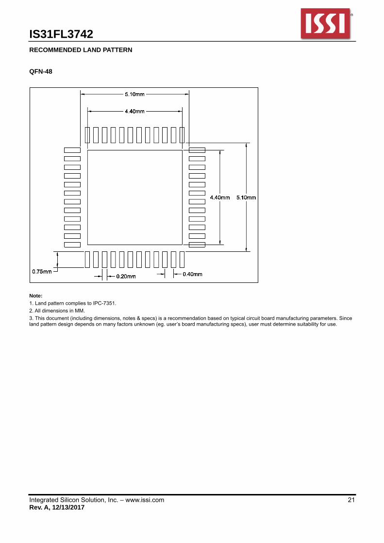
RECOMMENDED LAND PATTERN
QFN-48
Note:
1. Land pattern complies to IPC-7351.
2. All dimensions in MM.
3. This document (including dimensions, notes & specs) is a recommendation based on typical circuit board manufacturing parameters. Since land pattern design depends on many factors unknown (eg. user’s board manufacturing specs), user must determine suitability for use.
IS31FL3742
Integrated Silicon Solution, Inc. – www.issi.com 22 Rev. A, 12/13/2017
REVISION HISTORY
Revision Detail Information Date
0A Initial release. 2017.06.03
0B 1. Update the ILED formula 2. Update Land Pattern and θJA
2017.07.17
0C 1. Update Logic Electrical Characteristics Table 2017.09.06
0D 1. Update ESD value 2. Add SDB reset function description
2017.10.20
A Release to mass production 2017.12.13