deep level transient spectroscopic investigation of
TRANSCRIPT

ARTICLE
Deep level transient spectroscopic investigation ofphosphorus-doped silicon by self-assembledmolecular monolayersXuejiao Gao 1, Bin Guan 1, Abdelmadjid Mesli2, Kaixiang Chen1 & Yaping Dan 1
It is known that self-assembled molecular monolayer doping technique has the advantages of
forming ultra-shallow junctions and introducing minimal defects in semiconductors. In this
paper, we report however the formation of carbon-related defects in the molecular
monolayer-doped silicon as detected by deep-level transient spectroscopy and low-
temperature Hall measurements. The molecular monolayer doping process is performed
by modifying silicon substrate with phosphorus-containing molecules and annealing at high
temperature. The subsequent rapid thermal annealing drives phosphorus dopants along with
carbon contaminants into the silicon substrate, resulting in a dramatic decrease of sheet
resistance for the intrinsic silicon substrate. Low-temperature Hall measurements and sec-
ondary ion mass spectrometry indicate that phosphorus is the only electrically active dopant
after the molecular monolayer doping. However, during this process, at least 20% of the
phosphorus dopants are electrically deactivated. The deep-level transient spectroscopy
shows that carbon-related defects are responsible for such deactivation.
DOI: 10.1038/s41467-017-02564-3 OPEN
1 University of Michigan–Shanghai Jiao Tong University Joint Institute Shanghai Jiao Tong University, 800 Dong Chuan Road, Shanghai, 200240, China.2 Institut Matériaux Microélectronique Nanosciences de Provence, UMR 6242 CNRS, Université Aix-Marseille, 13397 Marseille Cedex 20, France. XuejiaoGao and Bin Guan contributed equally to this work. Correspondence and requests for materials should be addressed to Y.D. (email: [email protected])
NATURE COMMUNICATIONS | (2018) 9:118 |DOI: 10.1038/s41467-017-02564-3 |www.nature.com/naturecommunications 1
1234
5678
90():,;

Self-assembled molecular monolayer (SAMM) doping is apotential doping technique to tackle the challenges in theformation of sub-10-nm ultra-shallow junction1 and has the
advantage of facilitating mass production and applicability tosemiconductors like Si, Ge, InAs, GaAs, etc.2–5. In this technique,dopant-carrying molecules are first covalently immobilized on thesemiconductor surface via surface reactions. Due to surface self-limiting property, the areal dose of dopant molecules can bemodulated by varying reaction temperature6, reaction time6,molecule size7, and the composition of the molecules8,9. Subse-quently, the dopants are driven into the semiconductor bulk andactivated by thermal annealing. Unlike the technique of ionimplantation, no lattice damage is found during the dopant-incorporation process2,8,10. In addition, this technique is suitablefor doping in complex geometry structures, such as nanopillararrays4 or fins in fin-FETs11.
During the thermal annealing process, other atoms inthe molecular monolayer such as oxygen, hydrogen, andespecially carbon12 can be driven into silicon together with thedesired doping element. These impurities are difficult to detectdue to their atomic nature and low concentrations. It remainsan issue whether these unintentional impurities form complexdefects and how these defects affect the electrical properties ofthe substrate. Longo et al.13 have suspected the possible influenceof unintentional carbon contamination during the dopingprocess and hence reported a SAMM doping method to minimizecarbon incorporation by breaking chemical bonds and releasingcarbon at lower temperature than that of annealing. However,no detail information was given in their study on why carbonligand was removed before thermal annealing and how theyaffect the electrical properties of the substrate. Shimizu et al.12
investigated the diffusion behavior of carbon and oxygencontaminants in phosphorus-doped Si substrates by time-of-flightsecondary ion mass spectrometry (ToF-SIMS) and atomprobe tomography (APT), finding that the contaminants werelimited to the first atomic layer and could be easily removed.Puglisi and coworkers14 believed that a surface layer wheresilicon intermixed with carbon from dopant-carrying moleculeswas present after SAMM doping. However, with a significantsolubility in silicon and a diffusion coefficient larger than phos-phorus15, it is likely that carbon forms active defects, whichwould have significant influence on the electrical properties ofthe substrate. For example, interstitial carbon can bond withgroup V elements like substitutional phosphorus, arsenic, andantimony forming the pairs Ci–Ps, Ci–Ass, and Ci–Sbs withmultiple deep energy levels16 corresponding to several atomicconfigurations.
Deep-level transient spectroscopy (DLTS) is a very sensitivetechnique to study defects in bulk semiconductors, providinginformation on energy levels and concentrations of relateddefects17. Tremendous efforts have been made to acquire energylevels of impurities like carbon, oxygen, hydrogen, and theircomplex in silicon by using DLTS18–20. In this paper, we employDLTS to investigate defects formed by impurities in SAMM-doped silicon. The molecular monolayer grafting and doping arecharacterized by X-ray photoelectron spectroscopy (XPS) and vander Pauw measurements, respectively. The total phosphorusconcentration and the active fraction are determined by sec-ondary ion mass spectrometry (SIMS) and low-temperature Hallmeasurements, respectively. The DLTS study shows that carbon-related defects are present in the SAMM-doped silicon, resultingin the electrical annihilation of phosphorus dopants due tobonding with interstitial carbon.
ResultsWe fabricated phosphorus-functionalized silicon as outlinedin Fig. 1. Briefly, a freshly prepared hydrogen-terminated silicon(surface 1) was passivated with 5-hexenyl acetate (molecule 1)in Ar atmosphere at 95 °C for 16 h, yielding a surface withacetate terminus (surface 2). Subsequently the acetate surfacewas reduced into a hydroxyl-terminated surface (surface 3) bylithium aluminum hydride (LiAlH4) in tetrahydrofuron (THF)at 70 °C for 2 h. The hydroxyl groups on the surface werereacted with alkylphosphate (molecule 2) in the presence ofactivation agent dicyclohexylcarbodiimide (DCC), formingphosphate ester, thus rendering phosphorus-functionalizedsilicon (surface 4).
Each step of modification was characterized by XPS as shownin Fig. 2 and Supplementary Figure 1. High-resolution narrowscan of C 1s for surface 2 (Fig. 2a) reveals a broad peak at 285.0eV (FWHM 1.4 eV) related to aliphatic carbon-bonded carbon(C–C) from 5-hexenyl acetate. The broad peak has a side shoulderat 286.6 eV (FWHM 1.6 eV) attributed to oxygen-bonded carbon(C–O) and carbon adjunct to carbonyl (C(C=O)). The smallbump at 289.0 eV (FWHM 1.6 eV) is assigned to the carbon ofcarbonyl (C=O). The integral peak area ratio of C–C, C–O/C(C=O), and C=O is 6:2:1 consistent with the stoichiometric ratioof 5-hexenyl acetate (5:2:1) immobilized on the surface. To pro-vide a reference for surface 4 later, we also examined P 2s XPSspectrum of surface 2 ranging from 175 to 210 eV for phosphorussignal. As expected, no phosphorus was detected, except twobroad peaks (Fig. 2b) due to silicon plasmon loss21. For surface 3,the C 1s scan (Fig. 2c) shows the same three carbon components
H H H H H H H H H H H H H H H H
OO
OO
H H H H H H H
HO OO
H H H H H H H
O OOP
HO
O
O
10
O
OHO
PHO
O
O
10Molecule 1 Molecule 2
Si (100) Si (100) Si (100) Si (100)
Surface 1 Surface 2 Surface 3 Surface 4
Molecule 1
70 °C, 2 h DCC, DMFRT, 48 h
95 °C, 16 h
Molecule 2LiAlH4, THF
Fig. 1 Stepwise surface modification on Si (100) surfaces. Molecule 1 is chemically grafted onto surface 1 under thermal treatment at 95 °C for 16 h forminga molecular monolayer on surface 2. Molecule 2 reacts with the hydroxyl group on surface 3 leading to a phosphorus-funtionalized surface 4
ARTICLE NATURE COMMUNICATIONS | DOI: 10.1038/s41467-017-02564-3
2 NATURE COMMUNICATIONS | (2018) 9:118 |DOI: 10.1038/s41467-017-02564-3 |www.nature.com/naturecommunications

as on surface 2, namely C–C, C–O/C(C=O), and C=O, with apeak area ratio of 10:3:1. This indicates that about half of acetategroups on the surface have been reduced to hydroxyl. For surface4, the C 1s scan shows that the peak area ratio further increases to30:5:1 (Fig. 2d), suggesting that the alkylphosphate is successfullycoupled onto the Si surface. This successful coupling is alsosupported by an additional peak at 192.0 eV (FWHM 2.8 eV) inthe P 2s spectrum (Fig. 2e) which is assigned to phosphorus fromphosphate22.
To drive the molecular-monolayer-carried phosphorus into theintrinsic silicon substrate (>10 kΩ cm), the chemically modifiedSi samples were first coated with SiO2 made from spin-on-glass(SOG) and then annealed at 1050 °C for 2 min. The SiO2 layerwas later removed by buffered oxide etchant (BOE, HF:NH4F =6:1) before electrical characterizations. Van der Pauw four-pointmeasurements23 (Supplementary Note 1 and SupplementaryFigure 2) were performed in darkness on the unmodified Si(surface 1), annealed surface 3 (as a control to phosphorus-dopedsample), and surface 4 (phosphorus-doped sample). As shown inTable 1, the sheet resistance (Rs) for the control sample decreasesslightly from 317 (for the undoped silicon) to 226 kΩ/sq, indi-cating no significant contamination introduced in the process.For the phosphorus-doped sample, the resistance drops drama-tically to 1.06 kΩ/sq after doping. This suggests that the phos-phorus dopants have diffused into and electrically doped thesilicon substrate.
To examine the total amount of phosphorus incorporated intoSi, the phosphorus-doped sample was analyzed by SIMS. As
Cou
nts
(a.u
.)C
ount
s (a
.u.)
Cou
nts
(a.u
.)
Cou
nts
(a.u
.)C
ount
s (a
.u.)
294 292 290
C=O
C–O/ C(C=O)
C–C
C 1s
C 1s
C 1s
P 2s
P 2s P
Si 2s plasmon loss
288 286 284 282 280 210 205 200 195 190 185 180 175
Binding energy (eV)
294 292 290 288 286 284 282 280
Binding energy (eV)
294 292 290 288 286 284 282 280
Binding energy (eV)
Binding energy (eV)
210 205 200 195 190 185 180 175
Binding energy (eV)
a b
c
d e
Fig. 2 XPS spectra of modified silicon samples. a High-resolution narrow scans of C 1s and b P 2s obtained from 5-hexenyl acetate monolayers on silicon(surface 2 in Fig. 1). c C 1s spectrum of hydroxyl-terminated surface 3. d High-resolution scans of C 1s and e P 2s from phosphorus-modified silicon sample(surface 4)
Table 1 Sheet resistances of silicon samples via SAMMdoping technique by van der Pauw measurement
Si(100) intrinsic wafer, resistivity> 10 kΩ cm Rs(kΩ/sq)
Unmodified sample (surface 1) 317Control sample (annealed surface 3 with carbon monolayer) 226Phosphorus-doped sample (annealed surface 4) 1.06
NATURE COMMUNICATIONS | DOI: 10.1038/s41467-017-02564-3 ARTICLE
NATURE COMMUNICATIONS | (2018) 9:118 |DOI: 10.1038/s41467-017-02564-3 |www.nature.com/naturecommunications 3

shown in Fig. 3a, the distribution of phosphorus dopants ishighly non-uniform (see more discussions in SupplementaryNote 2). The phosphorus concentration drops from around3 × 1018 cm−3 by nearly three orders of magnitude within 200 nmbelow the surface. In terms of surface concentration, thephosphorus concentration per unit area is calculated to be1.34 × 1013 cm−2 by integrating all phosphorus from the surfaceto bulk. To find out the free electron concentration of thephosphorus-doped samples, we performed Hall measurements. InFig. 3b, the Hall resistance linearly changes with the appliedmagnetic field. The slope of the linear dependence is inverselyproportional to the free electron concentration as shown inEq. (1) from which the free electron concentration is found tobe 8.92 × 1012 cm−2. Note that Eq. (1) is on the assumptionof uniform doping. The non-uniform distribution of dopantsin our sample may lead to a few percent errors in the obtainedelectron concentration (see Supplementary Note 3 for more dis-cussions).
Ne ¼ � ΔBe ´ ðΔVH=IÞ
¼ � 1e ´ ðslopeÞ
¼ 11:6 ´ 10�19C ´ 70:1 m2 C�1
¼ 8:92´ 1012 cm�2
ð1Þ
in which e is the unit charge, VH is the Hall voltage, I is the sourcecurrent, B is the magnetic field, and Ne is the free electronconcentration per unit area.
Previously, it was reported that nitrogen carried by tert-butyl-N-allylcarbamate can electrically dope silicon24. To check whe-ther other impurities besides phosphorus dopants are also elec-trically active in our doped sample, low-temperature Hallmeasurements were performed as shown in Fig. 3c. The tem-perature was set from 80 K gradually up to 300 K. The electronconcentration per unit area was obtained from Hall measure-ments at each temperature (Supplementary Figure 3 and Sup-plementary Table 1). As the electron concentration as a functionof temperature follows Eq. (2)24, the activation energy of phos-phorus dopants was found as 42 meV by fitting Eq. (2) to theexperimental data, which is close to the known value (45 meV) ofphosphorus ionization energy in silicon25. This finding indicatesthat there is no significant amount of electrically active impuritiesother than phosphorus donors in the SAMM-doped sample.From the fitting, we also attained the concentration of electricallyactive phosphorus dopants, which is 1.07 × 1013 cm−2. The freeelectrons in the doped sample are believed to originate from thispart of phosphorus dopants. Thus, the ionization rate at roomtemperature is estimated to be 83.4% if we divide the electronconcentration (8.92 × 1012 cm−2) by the electrically active
phosphorus dopants (1.07 × 1013 cm−2). This ionization rate isreasonable, considering that the ionization rate of phosphorusdopants in high concentration (about 1018 cm−3 in particular) isas low as 80%26,27. Quantitatively, a theoretical ionization rate forelectrically active phosphorus with the same distribution andconcentration (1.07 × 1013 cm−2) was calculated considering theeffects of the incomplete ionization26,27 and internal electric field.The resultant ionization rate is 81.3% (Supplementary Note 4 andSupplementary Figure 4), in good agreement with the experi-mental value. It means that this part (1.07 × 1013 cm−2) of elec-trically active phosphorus fits the classical case for phosphorusdonors in silicon. Note that the total phosphorus dopant con-centration detected by SIMS is 1.34 × 1013 cm−2. The interestingquestion is what happened to the remaining 20% (=(1.34 − 1.07)/1.34) of the phosphorus dopants (0.27 × 1013 cm−2). We speculatethat the remaining phosphorus dopants are electrically annihi-lated by carbon-related defects.
nc ¼�Nc þ
ffiffiffiffiffiffiffiffiffiffiffiffiffiffiffiffiffiffiffiffiffiffiffiffiffiffiffiffiffiffiffiffiffiffiffiffiffiffiffiffiffiN2
c þ 8NcNDexp ΔEkT
� �q4exp ΔE
kT
� � ð2Þ
where Nc is the effective density of states function which is
defined as Nc � 2 2πm�nkT
h2
� �32¼ wðkTÞ32 with w being the constant
related to the band structure of the semiconductor, ND is theconcentration of donors, and ΔE is the activation energy which isequal to (Ec − Ed) with Ec and Ed being the conduction band edgeand the donor energy level, respectively.
To verify this hypothesis, DLTS measurements were performedon SAMM-doped samples. DLTS requires a Schottky contact tobe formed on top of the SAMM-doped surface (Fig. 4a). Thedepletion region of the Schottky junction will be readily extendedinto the substrate bulk if an intrinsic substrate is used. As aresult, the information extracted from DLTS will be mostly ori-ginating from the bulk. However, the impurities and defectsintroduced by the SAMM doping are dominantly located near thesurface. To detect possible defects in this region, we prepared aset of new samples on phosphorus-doped n-type Si (100)substrate with a resistivity of 1–3Ω cm (phosphorus concentra-tion 1 – 5 × 1015 cm −3; carbon concentration <5 × 1016 cm−3) toconfine the Schottky depletion region near the surface. The sameSAMM doping process as described previously (on SAMM-dopedsurface 4) was conducted on the n-type substrate. The successfuldoping of phosphorus into the substrate was confirmed by SIMS(Fig. 4c). To form Schottky contact, a 150-nm-thick Au electrodewas evaporated directly on the SAMM-doped surface, which hadbeen cleaned with Piranha solution and hydrofluoric acid. Al filmwas evaporated on the back side of the substrate that had been
1019 120
6×10¹²
ΔE = 0.042 eV
80080 K120 K160 K240 K
–800
–1 0 1Magnetic field (T)
0
Nd = 1.07×1013 cm–25×1012
4×10¹²
3×10¹²
Car
rier
conc
entr
atio
n (c
m–2
)
2×10¹²
1×10¹²
0.006 0.009 0.012 0.015
Hal
lre
sist
ance
(Ω
)
0.018 0.021
kT (eV)
0
80
40
Slope = –70.1 (m2 C–1)
Hal
l res
ista
nce
(Ω)
0
–40
1018
1017
1016
1015
1014
0 50 100 150 200
Doping depth (nm)
Con
cent
ratio
n (c
m–3
)
250 300 350 400 –1.0 –0.5 0.0 0.5 1.0
Magnetic field (Tesla)
a b c
Fig. 3 Dopant ionization rate. a Doping profile of phosphorus-doped Si measured by SIMS. b Hall resistance versus magnetic field measured by Hallmeasurement at room temperature. c Free electron concentration versus temperature. Inset: Hall measurements of phosphorus-doped Si at severaltemperatures
ARTICLE NATURE COMMUNICATIONS | DOI: 10.1038/s41467-017-02564-3
4 NATURE COMMUNICATIONS | (2018) 9:118 |DOI: 10.1038/s41467-017-02564-3 |www.nature.com/naturecommunications

extensively scratched by a diamond scribe. The scratch createsdefects, which reduce the minority carrier lifetime and thereforefacilitate the formation of Ohmic contact between the Al filmand n-type silicon substrate (Supplementary Figure 5). No post-annealing was conducted to avoid Au/Al diffusion intosilicon. The device schematic is shown in the inset of Fig. 4a.A typical I–V curve of the device is depicted in Fig. 4a, evidencingthat a Schottky diode is formed. A similar process was alsoapplied to the blank and control sample (both are n-type) toform Schottky contacts (Supplementary Figure 6) for DLTSmeasurements. The blank sample went through the SiO2 cappingand annealing process without any functionalization. Thecontrol sample went through all the processes except thatthe alkylphosphate was not added during esterification reaction,like surface 3 in Fig. 1.
The voltage-dependent capacitance of the Schottky junctionswas first measured at 1 MHz with the dc bias sweeping from −2 to0 V for the control sample and from −2 to 0.3 V for the SAMM-doped sample. Figure 4b shows the C–V dependence in form of 1/C2 versus dc voltage bias. For the control sample, the dependenceis linear and the build-in potential is extracted as 0.57 V from theintercept with x coordinate. As expected, this built-in potentialincreases to 0.76 V as the temperature is lowered to 50 K (Sup-plementary Figure 7). For the SAMM-doped sample, the depen-dence of 1/C2 on dc voltage bias is nonlinear due to the highlynon-uniform distribution of phosphorus dopants introduced bythe SAMM doping process. This nonlinearity makes it unreliableto extract the built-in potential. But the ionized charge profile canbe extracted, shown in red dots in Fig. 4c. The concentration ofionized charges in the control sample is around 3 × 1015 cm−3
(black dots in Fig. 4c) consistent with the nominal resistivity
(1 – 3Ω cm) of the n-type Si substrate. In contrast, the ionizedcharge concentration in the SAMM-doped sample drops fromabout 2 × 1016 cm−3 at a depth of 140 nm to about 3 × 1015 cm−3
at about 330 nm, indicating that SAMM-introduced phosphorusdiffuses beyond 300 nm. Note that the phosphorus concentrationfrom SIMS (blue lines) is constant at about 1016 cm−3 startingfrom a depth of 200 nm below the surface due to the rela-tively high detection limit of the SIMS technique.
DLTS measurements were performed on the samples at bias of−2 V with applied pulse of 0 V (hereafter it is written in form of“bias voltage”–“pulse voltage”, i.e., −2 to 0 V) as shown in Fig. 4d.No peaks are detected for the blank sample (black curve),demonstrating that there is nearly no defects in bare silicon waferand that the capping layer and the annealing process introduce nodefects into silicon. For the carbon-chains-functionalized controlsample (red curve), a tiny kink at 75 K (Fig. 4d inset) and a visiblepeak at 155 K next to a broad bump from 200 to 300 K areobserved, indicating that carbon from the dopant-carryingmolecules can diffuse into the substrate and produce somedefects in phosphorus-doped Si. These defects could be related toC, H, O, and N. Oxygen plays a significant role only in thepresence of lattice defects such as vacancies28 which do not existin the doping process considered in this work. Defects involvinghydrogen are very unlikely as they do not exist after the hightemperature treatments during which hydrogen out diffuses29.Finally, nitrogen if electrically active has very shallow energylevels, and thus none of the observed levels can be associated withthis impurity, unless nitrogen binds to other unknown defects30.Therefore, we would attribute most of the observed defects tocomplexes where carbon is the main ingredient. For the sampledoped by the molecular-monolayer-carried phosphorus (SAMM-
1.5×10²⁰
1.0×10²⁰
5.0×10¹⁹
10–3
10–4
Cur
rent
(A
)C
once
ntra
tion
(cm
–3)
10–5
10–6
1018
1017
1016
1015
–2.0 –1.6 –1.2 –0.8
Voltage (V)
–0.4 0.0 0.4 –2.0 –1.5 –1.0 –0.5 0.0 0.5 1.0Voltage (V)
1/C
2 (F
–2)
Blank sample
Au schottky contact
AI ohmic contact
Doping region
Silicon
Control samplePhosphorus-doped sample
SAMM-doped sample 50 KControl sample 300 K
0.5
0.4
0.3
0.2
0.1
0.0
0.005
0
70 80
Temperature (K)
DLT
S (
pF)
Depletion width (nm)50 150 2502001000 200 400 600 800 1000 300
0.0
Control sample 300 K
P in SAMM-doped sampleSAMM-doped sample 50 K
a
c d
b
Fig. 4 IV, CV, and DLTS data on SAMM-doped phosphorus-doped silicon. a I–V curve of the Schottky diode made on the SAMM-doped sample with theinset schematically showing the diode structure. b Capacitance as a function of bias voltage in form of 1/C2 versus V. c Charge carrier concentration atdifferent depth derived from b. As a reference, phosphorus depth profile by SIMS is also presented in blue curve. d Comparison of DLTS spectra of theblank sample, control sample, and SAMM-doped sample with reversed-bias pulse from −2 to 0 V, at the rate window of 200 s−1. The inset shows thespectra at the range of 65–85 K
NATURE COMMUNICATIONS | DOI: 10.1038/s41467-017-02564-3 ARTICLE
NATURE COMMUNICATIONS | (2018) 9:118 |DOI: 10.1038/s41467-017-02564-3 |www.nature.com/naturecommunications 5
doped sample, blue curve), the kink at 75 K is absent (Fig. 4dinset), whereas the peak at 155 K and the broad bump both growmuch bigger than the corresponding peaks in the control sample,probably due to the increase in defect concentration brought byextra amount of carbon and phosphorus. What is more, the shapeof the broad bump is skewed in comparison with the controlsample, clearly because the closely spaced peaks in the bumpincrease differently in amplitude. By comparing the three curvesin Fig. 4d, we conclude that the SAMM doping process producesdefects in phosphorus-doped silicon.
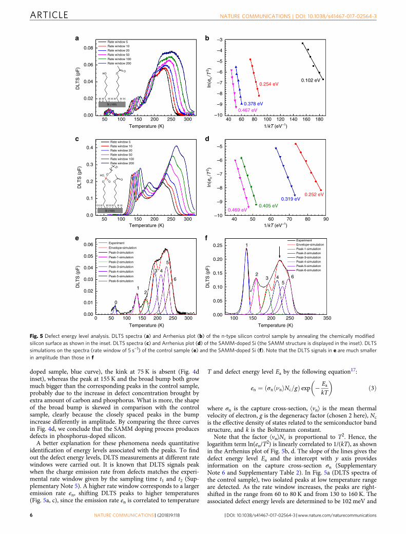
A better explanation for these phenomena needs quantitativeidentification of energy levels associated with the peaks. To findout the defect energy levels, DLTS measurements at different ratewindows were carried out. It is known that DLTS signals peakwhen the charge emission rate from defects matches the experi-mental rate window given by the sampling time t1 and t2 (Sup-plementary Note 5). A higher rate window corresponds to a largeremission rate en, shifting DLTS peaks to higher temperatures(Fig. 5a, c), since the emission rate en is correlated to temperature
T and defect energy level Ea by the following equation17:
en ¼ ðσn νnh iNc=gÞ exp � EakT
� �ð3Þ
where σn is the capture cross-section, ⟨vn⟩ is the mean thermalvelocity of electron, g is the degeneracy factor (chosen 2 here), Nc
is the effective density of states related to the semiconductor bandstructure, and k is the Boltzmann constant.
Note that the factor ⟨vn⟩Nc is proportional to T2. Hence, thelogarithm term ln(en/T2) is linearly correlated to 1/(kT), as shownin the Arrhenius plot of Fig. 5b, d. The slope of the lines gives thedefect energy level Ea and the intercept with y axis providesinformation on the capture cross-section σn (SupplementaryNote 6 and Supplementary Table 2). In Fig. 5a (DLTS spectra ofthe control sample), two isolated peaks at low temperature rangeare detected. As the rate window increases, the peaks are right-shifted in the range from 60 to 80 K and from 130 to 160 K. Theassociated defect energy levels are determined to be 102 meV and
DLT
S (
pF)
In(e
n /T
2 )In
(en
/T2 )
DLT
S (
pF)
DLT
S (
pF)
DLT
S (
pF)
0.08
0.06
0.04
0.02
0.0050 150 250 300200100
Temperature (K)
–3
–4
–5
–6
–7
–8
–9
–10
–5
–6
–7
–8
–9
–1050 150 250 300200100
OO
PO
10
O
OHO
H H H HH
Si (100)
HH
Temperature (K)
0.4
0.3
0.2
0.1
0.0
1
1
2
2
3
34
4
5
5
66
0
ExperimentEnvelope-simulationPeak-1-simulationPeak-2-simulationPeak-3-simulationPeak-4-simulationPeak-5-simulationPeak-6-simulation
0.25
0.20
0.15
0.10
0.05
0.00
0.06
0.05
0.04
0.03
0.02
0.01
0.00500 150 250 300200100 150 250 300 350200100
Temperature (K) Temperature (K)
40
40 50 60
0.469 eV
0.467 eV
0.405 eV0.319 eV
0.378 eV
0.252 eV
0.102 eV0.254 eV
70 80 90
60 80 100 120 140 160 180
1/kT (eV–1)
1/kT (eV–1)
Experiment
Rate window 5Rate window 10Rate window 20Rate window 50Rate window 100Rate window 200
Envelope-simulation
Peak-1-simulation
Peak-0-simulation
Peak-2-simulation
Peak-3-simulation
Peak-4-simulation
Peak-5-simulation
Peak-6-simulation
Rate window 5Rate window 10Rate window 20Rate window 50Rate window 100Rate window 200
OOHO
H H H HH
Si (100)
HH
a b
dc
fe
Fig. 5 Defect energy level analysis. DLTS spectra (a) and Arrhenius plot (b) of the n-type silicon control sample by annealing the chemically modifiedsilicon surface as shown in the inset. DLTS spectra (c) and Arrhenius plot (d) of the SAMM-doped Si (the SAMM structure is displayed in the inset). DLTSsimulations on the spectra (rate window of 5 s−1) of the control sample (e) and the SAMM-doped Si (f). Note that the DLTS signals in e are much smallerin amplitude than those in f
ARTICLE NATURE COMMUNICATIONS | DOI: 10.1038/s41467-017-02564-3
6 NATURE COMMUNICATIONS | (2018) 9:118 |DOI: 10.1038/s41467-017-02564-3 |www.nature.com/naturecommunications

254 meV (Fig. 5b), respectively. Considering that the only speciesreally involved in the control sample are possibly carbon-relateddefects as mentioned above, the defect energy level at 102 meVcan be best ascribed to carbon interstitials31, configuration ofwhich is shown in Supplementary Figure 8. The defect energylevel at 254 meV continues to appear in the SAMM-doped sample(252 meV) with a higher amplitude. A defect energy level at 319meV is extracted for the SAMM-doped sample from the isolatedpeak shifting from 155 to 190 K in Fig. 5c. At the region oftemperature above 200 K, two main peaks with associated energylevels at 378 meV and 467 meV can be identified from the bumpfor the control sample (Fig. 5a, b). Similarly, two energy levels at405 meV and 469 meV are identified for the SAMM-dopedsample in Fig. 5c, d. However, the broad bumps in the DLTSspectra (Fig. 5a, c), clearly consisting of multiple closely spacedpeaks may even contain more than those identified main peaks.
To identify the peaks in the broad bumps more accurately,DLTS simulations were conducted according to the basic prin-ciple as illustrated below, and the results were displayed in Fig. 5e,f. For DLTS, capacitance transient starts at the end of excitationpulse and then decays exponentially in its simplest form. Theamplitude of a single peak detected at a given rate window can beexpressed as Eq. (4).
ΔC ¼ ΔC0 exp �ent1ð Þ � exp �ent2ð Þð Þ ð4Þ
where ΔC0 is the initial capacitance transient (capacitance tran-sient at the end of excitation pulse), and t1 and t2 defines the ratewindow. The emission rate en is given by Eq. (3).
For multiple defect levels, the DLTS signal can be written as Eq.(5) (refer to Supplementary Equation (11)).
ΔC ¼X
ΔC0i exp �enit1ð Þ � exp �enit2ð Þð Þ ð5Þ
in which i represents the ith defect.Table 2 summarizes the defect energy levels of the control and
the SAMM-doped samples. The energy levels in bold are derivedfor the bias pulse from −2 to 0 V from both Arrhenius plots(number without underline) and simulation results (number withunderline). The rest are for the other bias pulses, meaning that theDLTS are probing other regions, which will be discussed later. Allthe energy levels are in comparison with those of interstitial-carbon–substitutional-phosphorus (Ci–Ps) pairs from literature(the last row in Table 2). Five out of six energy levels for theSAMM-doped sample are consistent with the energy levels ofCi–Ps pairs reported previously. Only peak 5 at the energy levelnear 467 meV or 469 meV is found independently in both controland SAMM-doped samples, suggesting that this defect energylevel does exist despite not showing in ref. 32. It is probably due toN-related defects16 rather than Ci–Ps multi-configurable defects,since the activation agent (DCC) and solvent (dimethylfoma-mide) in the SAMM grafting process contain nitrogen. Peak 4 inthe SAMM-doped sample is determined by simulations to be 390
meV instead of 405 meV as shown in the Arrhenius plot inFig. 5d. The peak at 405 meV indicated by the arrow in Fig. 5f isthe result of overlap between peak 4 and peak 5. Note that thecontrol sample is n-type silicon with phosphorus-doping con-centration of 3 × 1015 cm−3 as purchased. Therefore, all the Ci–Psrelated energy levels shown up in the SAMM-doped sample alsoappear in the control sample (but with much smaller magnitude),because the carbon defects can bind with both the SAMM-introduced phosphorus dopants and the background phosphorusdopants in the n-type Si substrate (Fig. 4d). It is worth pointingout that the DLTS envelope by simulations does not match theexperimental results perfectly. Some other peaks clearly exist,which may originate from surface states, nitrogen con-taminants33, or atomic disorder34. The full deconvolution of theDLTS spectra can be found in Supplementary Figures 9–11 andSupplementary Table 3.
To show clearly that carbon defects bind with phosphorusdopants introduced by the SAMM doping process, we tuned thebias voltages from −2 to 0 V and injection pulses from −1 to 0.2V, pushing the DLTS probing region from bulk to near the sur-face (Fig. 6)35–37. For comparison, SIMS profiling was also per-formed for phosphorus and carbon in both the SAMM-dopedsample and the blank sample, as shown in Fig. 6a. The back-ground phosphorus doping (3 × 1015 cm−3) is detected by CVtechnique (pink curve) but not by SIMS (blue curve and greentriangles) due to the relatively high detection limit of SIMS. Acombination of SIMS and CV measurements indicates that theSAMM-introduced phosphorus dopants has a concentration ofaround 2 × 1018 cm−3 near the surface and rapidly declines to thebackground doping concentration of 3 × 1015 cm−3 at a depth of300 nm below the surface. The certificated carbon concentrationin our n-type Si substrate is <5 × 1016 cm−3. The carbon SIMSdata reaches a floor at 2 × 1016 cm−3 in both the SAMM-dopedsample and the blank sample, meaning that the actual back-ground carbon concentration in the substrate is at this level oreven lower. The concentration of carbon impurities introduced bythe SAMM doping process is ~2 × 1018 cm−3 at the surface butslowly decays to 2 × 1016 cm−3 at a distance of about 300 nm fromthe surface. When the bias pulses to 0.2 from 0 V bias at 300 K,the depletion region edge sweeps approximately from 100 to 64nm below the surface, in which carbon and phosphorus impu-rities mainly come from the SAMM, as shown in Fig. 6b. Notethat the depletion region moves slightly deeper into the substrateat low temperature (Supplementary Figures 12 and 13 and Sup-plementary Table 4). Fig. 6c depicts the corresponding DLTS datawithin the above sweep range of the depletion region. All thepeaks shown here are included in Table 2. DLTS is repeated atother bias pulses. The probing range and corresponding DLTSdata are shown in Fig. 6d–i (also see the defects energy levels inTable 2). A detailed analysis on the peak positions and amplitudeswill not be conclusive due to the well-known metastability ofcarbon-related complex defects32. But overall the experimental
Table 2 Comparison of the energy levels derived from DLTS spectra, simulations and energy levels of Ci–Ps from ref. 32
Isolated peaks (meV) Bump area (meV)
Bias pulse Peak 0 Peak 1 Peak 2 Peak 3 Peak 4 Peak 5 Peak 6
Control sample −2 to 0 V 102 254 319 378 390 467 480SAMM -doped sample −2 to 0 V -- 252 319 380 390 (405) 469 480
−2 to −1V -- 260 319 380 390 467 480−0.2 to 0.2 V -- 260 319 380 390 467 --0 to 0.2V -- 260 319 -- 390 467 --
Ci–Ps (ref. 32) -- 260 320 380 390 -- 480
“--”means no peak is detected or has been reported in that position. The underscored energy levels are derived from simulations
NATURE COMMUNICATIONS | DOI: 10.1038/s41467-017-02564-3 ARTICLE
NATURE COMMUNICATIONS | (2018) 9:118 |DOI: 10.1038/s41467-017-02564-3 |www.nature.com/naturecommunications 7

observations are consistent with the fact that a larger quantity ofcarbon and phosphorus impurities in a probing region will lead tostronger DLTS signals. For example, though the probing regionwidth in Fig. 6h is larger than that in Fig. 6d, the correspondingDLTS signals in Fig. 6i are much weaker because the DLTS isprobing a region deep in the bulk (Fig. 6h) where the phosphorusand carbon concentration are much lower.
DiscussionIt is known that ultra-shallow junctions as the source and drain ofmodern complementary metal–oxide–semiconductor (CMOS)transistors help suppress the short channel effect8. The SAMMdoping technique has the unique advantage of forming ultra-shallow junctions8. However, the ultra-scaled thickness of thejunctions will inevitably increase series resistance in the sourceand drain, resulting in inferior performances for CMOS transis-tors. A possible solution is to increase the dopant concentrationby increasing the molar ratio of dopant elements in the carriermolecule as demonstrated previously38. However, according tothe carbon defect formation mechanism, a higher phosphorusconcentration may lead to a larger portion of inactive phos-phorus, offsetting the effect of higher dopant molar ratio onreducing the series resistance. Logically, new processes should be
developed to remove carbon in dopant carrying molecules priorto thermal annealing so that the Ci–Ps defects can be minimizedto achieve a high ionization rate for phosphorus dopants.
In conclusion, we have successfully doped silicon with phos-phorus by SAMM doping technique via a two-step molecularmonolayer grafting process. Phosphorus is incorporated intosilicon with an areal dose of 1.34 × 1013 cm−2. However, only 80%(1.07 × 1013 cm−2) of phosphorus is electrically active and the rest20% is deactivated. Carbon diffuses into silicon together withphosphorus but with a much deeper depth. This carbon can bondwith group V element forming complex defects. Correspondingdeep energy levels are detected by DLTS for the first time inSAMM doping technique. With the assistance of DLTS simula-tion, multi-configurational defects Ci–Ps are confirmed, indicat-ing that phosphorus dopants are partially deactivated byinterstitial carbon. Therefore, for SAMM doping technique, car-bon in dopant-carrying molecules is recommended to be removedor controlled at low concentration before thermal annealing.
MethodsMaterials. FZ single-side polished silicon wafers, (100)-oriented (⟨100⟩± 0.05°),500± 25 μm thick, >10 kΩ cm in resistivity, and CZ single-side polished siliconwafers (100)-oriented (⟨100⟩± 0.05°), n-type (phosphorus), 500± 10 μm thick, 1–3
Con
cent
ratio
n (c
m–3
)E
nerg
y (e
V)
Ene
rgy
(eV
)E
nerg
y (e
V)
Ene
rgy
(eV
)
2
1
0
–1
Depth from the surface (nm) Temperature (K)
–2 V – –1 VEnvelope
–2 V – 0 VEnvelope
–0.2 V – 0.2 VEnvelope
0 V – 0.2 VEnvelope
0 200 400 600 800 1000 50 100 150 200 250 300
0.6
0.0
–0.6
0.3EC
EF
EV
EV
EC
EV
EF
EC
EV
EF
EC
EF
0.0
0.3
0.0
0.3
0.0
0.3
DLT
S (
pF)
DLT
S (
pF)
DLT
S (
pF)
DLT
S (
pF)
0.0
0 V
0.2
V0.
2 V
–0.2
V
0 V
–2 V
–2 V
–1 V
0.6
1015
1016
1017
1018
1019
0.0
–0.6
2
1
0
–1
C in blank sampleP in blank sampleC in SAMM-doped sampleP in SAMM-doped sampleCharge profile from CV
a
b
d
f
h
c
e
g
i
Fig. 6 DLTS probing region analysis. a Phosphorus and carbon depth profiles by SIMS compared with ionized charge profile derived from CV. Silvacosimulation on band structure at 300 K with bias voltage of 0 V (b), −0.2 V (d), −2 V (f) and −2 V (h). Probing regions are shaded in gray with differentpulses from 0 to 0.2 V (b), −0.2 to 0.2 V (d), −2 to 0 V (f) and from −2 to −1 V (h). DLTS simulations on the spectra of the SAMM-doped silicon withpulses from 0 to 0.2 V (c), −0.2 to 0.2 V (e), −2 to 0 V (g) and −2 to −1 V (i). The rate windows of DLTS spectra are 200 s−1. Note that c, e, g and i havethe same y axis scale for better comparison. A close-up figure for i to show the fitting envelope can be found in Supplementary Figure 11
ARTICLE NATURE COMMUNICATIONS | DOI: 10.1038/s41467-017-02564-3
8 NATURE COMMUNICATIONS | (2018) 9:118 |DOI: 10.1038/s41467-017-02564-3 |www.nature.com/naturecommunications

Ω cm in resistivity, were purchased from Suzhou Resemi Semiconductor Co. Ltd.,China. All chemicals, unless noted otherwise, were of analytical grade and used asreceived. Isopropanol, acetone, and ethanol for surface cleaning were of CMOSgrade. 5-Hexenyl acetate (98%) was purchased from TCI, Shanghai. Mono-N-dodecyl phosphate (97%) was from Alfa Aesar. Dicyclohexylcarbodiimide (DCC,99%), lithium aluminum hydride (LiAlH4 powder, reagent grade, 95%), andhydrofluoric acid (HF, 48%, CMOS grade) were from Sigma Aldrich.
Wafer cleaning. Si wafers were cleaved into 1.5 cm by 1.5 cm pieces and cleanedwith acetone and ethanol of CMOS grade in a sonication bath for 5 min, respec-tively. After rinsed with deionized (DI) water, the Si samples were immersed in“piranha solution” (98% H2SO4:30% H2O2, 3:1 (v/v)) for 30 min at 90 °C, followedby rinsing with DI water again. The wafers were then etched in 2.5% HF solutionfor 90 s to remove the oxide layer and render a hydrogen-terminated surface. Thehydrogen-terminated samples were quickly rinsed in DI water, blown dry withnitrogen, and immediately proceeded to further modification.
Thermal hydrosilylation and surface functionalization. First, 5-hexenyl acetatewas grafted onto Si by hydrosilylation reaction. The freshly etched Si (100) sampleswere immediately transferred to a deoxygenated sample of neat 5-hexenyl acetatein a dry Schlenk tube under Ar atmosphere. The reaction was then conducted at 95°C in Ar atmosphere for 16 – 19 h. The resulting samples were copiously rinsedwith ethanol, dichloromethane, and acetone, respectively, and then blown dried bya stream of N2.
Subsequently, the acetate-terminated surface was immersed in drytetrahydrofuran (THF) with 5% (w/v) LiAlH4 and refluxed at 70 °C for 2 h. Afterrinsing with DI water and ethanol, the hydroxyl-terminated samples wereimmersed into 0.5 M hydrochloric acid for 20 min to remove any Al residues.
In the presence of bifunctional crosslinker DCC (40 mM), the hydroxyl-terminated samples were reacted with mono-dodecyl phosphate (5 mΜ) indimethylfomamide (DMF) at room temperature for 48 h, affording phosphorus-containing functionalization. The samples were washed carefully with ethanol,dichloromethane, and acetone to remove any remaining coupling reagents anddried under N2 stream for further treatments.
Silicon dioxide deposition and thermal annealing. SiO2 capping layers on siliconwere produced by SOG method with IC1-200 polysiloxane-based coating material(Futurrex Inc. USA). Briefly, silicon wafer was spin-coated with the IC1-200 at3000 rpm for 40 s, followed by 100 °C bake on a hot plate for 60 s, 200 °C for 60 sand 400 °C bake in Ar for 30 min. After the formation of the capping layers, thefunctionalized silicon samples were thermally annealed at 1050 °C for 120 s, with aramp temperature of 100 °Cmin−1, starting from 800 °C, in Ar environment in atube furnace (Thermo scientific Lindberg/Blue, USA). After annealing, the doped Sisamples were immersed in BOE (buffer oxide etchant) solution (HF:NH4F = 6:1,CMOS grade, J.T. Baker Co. USA) to remove SiO2 layer.
Surface characterization. XPS was carried on a Kratos AXIS UltraDLD spec-trometer with a monochromated Al Kα source (1486.6 eV), a hybrid magnificationmode analyzer and a multichannel detector at a takeoff angle of 90° from the planeof the sample surface. Analysis chamber pressure is <5 × 10⁻⁹ Torr. All energies arereported as binding energies in eV and referenced to the C 1s signal (corrected to285.0 eV) for aliphatic carbon on the analyzed sample surface. Survey scans werecarried out selecting 250 ms dwell time and analyzer pass energy of 160 eV. High-resolution scans were run with 0.1 eV step size, dwell time of 100 ms and theanalyzer pass energy set to 40 eV. After background subtraction using the Shirleyroutine, XPS spectra were fitted with a convolution of Lorentzian and Gaussianprofiles by using software Casa XPS. Secondary-ion mass spectrometry (SIMS) wasconducted to obtain dopant profile at the top 500 nm of substrate by EvansAnalytical Group, NJ, USA.
Van der Pauw and Hall measurements. The metal contacts on silicon for elec-trical measurements were realized by evaporating 200-nm aluminum or aluminum/gold films in a thermal evaporation system (Angstrom Engineering, Canada). Vander Pauw measurements were performed on square-shaped samples on which themetal contacts are exactly located at the four corners. The custom-made probestation shrouded in a completely dark metal box is equipped with four solidtungsten probe tips (the tip size < 1 μm). Keithley 2400 source meter units and acustom-written Labview script were employed to generate and collect current/voltage data. Hall measurements were performed on the same square-shapedsamples, which were pre-mounted onto a dc resistivity sample holder via wirebonding, in a Physical Property Measurement System (PPMS, Quantum Design,USA).
DLTS. Schottky diodes for DLTS measurement are fabricated by depositing a circleAu electrode of 1 mm in diameter and 150 nm thick on the top of silicon and 150nm thick Al on the backside via thermal evaporation (Angstrom Engineering,Canada). The circle Au electrode is deposited with assistance of lithographytechnique. The diodes are then mounted onto sample holder TO5. A conventional
DLTS with boxcar mode are applied to get better resolution. Data were collectedusing Laplace DLTS software and plotted in usual DLTS plots.
SIMS. The carbon and phosphorus SIMS profiling was conducted at EAGlaboratories in USA under high vacuum condition of about 3 × 10⁻¹¹ Torr. FocusedCs+ primary ion beam was applied for sputtering, which facilitate high yields ofsecondary ions of phosphorus and carbon. Before sputtering, the samples werecleaned with oxygen plasma to remove possible carbon contamination from air.
Data availability. The data that support the findings of this study are availablefrom the authors on reasonable request, see author contributions for specific datasets.
Received: 14 September 2016 Accepted: 11 December 2017
References1. Ho, J. C. et al. Wafer-scale, sub-5 nm junction formation by monolayer doping
and conventional spike annealing. Nano Lett. 9, 725–730 (2009).2. Ho, J. C. et al. Nanoscale doping of InAs via sulfur monolayers. Appl. Phys. Lett.
95, 072108 (2009).3. Zhang, S., Sugioka, K., Fan, J., Toyoda, K. & Zou, S. Studies on excimer laser
doping of GaAs using sulphur adsorbate as dopant source. Appl. Phys. A 58,191–195 (1994).
4. Cho, K. et al. Molecular monolayers for conformal, nanoscale doping of InPnanopillar photovoltaics. Appl. Phys. Lett. 98, 203101 (2011).
5. Collins, G. & Holmes, J. D. Chemical functionalisation of silicon andgermanium nanowires. J. Mater. Chem. 21, 11052–11069 (2011).
6. Arduca, E. et al. Synthesis and characterization of P δ-layer in SiO2 bymonolayer doping. Nanotechnology 27, 075606 (2016).
7. Long, B. et al. in Proc. 20th International Conference on Ion ImplantationTechnology (IIT) (IEEE, Portland, OR, USA, 2014).
8. Ho, J. C. et al. Controlled nanoscale doping of semiconductors via molecularmonolayers. Nat. Mater. 7, 62–67 (2008).
9. Ye, L. et al. Controlling the dopant dose in silicon by mixed-monolayer doping.ACS Appl. Mater. Interfaces 7, 3231–3236 (2015).
10. Kong, E. Y.-J., Guo, P., Gong, X., Liu, B. & Yeo, Y.-C. Toward conformaldamage-free doping with abrupt ultrashallow junction: formation of Simonolayers and laser anneal as a novel doping technique for InGaAsnMOSFETs. IEEE Trans. Electron Devices 61, 1039–1046 (2014).
11. Ang, K.-W. et al. in Proc. 2011 IEEE International Electron Devices Meeting(IEDM) (IEEE, Washington DC, USA 2011).
12. Shimizu, Y. et al. Behavior of phosphorous and contaminants from moleculardoping combined with a conventional spike annealing method. Nanoscale 6,706–710 (2014).
13. Longo, R. C., Cho, K., Schmidt, W. G., Chabal, Y. J. & Thissen, P. Monolayerdoping via phosphonic acid grafting on silicon: microscopic insight frominfrared spectroscopy and density functional theory calculations. Adv. Funct.Mater. 23, 3471–3477 (2013).
14. Caccamo, S. et al. Silicon doped by molecular doping technique: role of thesurface layers of doped Si on the electrical characteristics. Mater. Sci. Semicond.Process. 42, 200–203 (2016).
15. Goesele, U., Laveant, P., Scholz, R., Engler, N. & Werner, P. Diffusionengineering by carbon in silicon. in MRS Proceedings (Cambridge UniversityPress, 2011).
16. Gürer, E. & Benson, B. Multiconfigurational carbon-group V pair defects insilicon. in MRS Proceedings (Cambridge University Press, 1989).
17. Lang, D. Deep-level transient spectroscopy: a new method to characterize trapsin semiconductors. J. Appl. Phys. 45, 3023–3032 (1974).
18. Pensl, G., Schulz, M., Hölzlein, K., Bergholz, W. & Hutchison, J. New oxygendonors in silicon. Appl. Phys. A 48, 49–57 (1989).
19. Endrös, A., Krühler, W. & Koch, F. Electronic properties of the hydrogen-carbon complex in crystalline silicon. J. Appl. Phys. 72, 2264–2271 (1992).
20. Asom, M., Benton, J., Sauer, R. & Kimerling, L. Interstitial defect reactions insilicon. Appl. Phys. Lett. 51, 256–258 (1987).
21. Gouzman, I., Dubey, M., Carolus, M. D., Schwartz, J. & Bernasek, S. L.Monolayer vs. multilayer self-assembled alkylphosphonate films: X-rayphotoelectron spectroscopy studies. Surf. Sci. 600, 773–781 (2006).
22. Dubey, M., Gouzman, I., Bernasek, S. L. & Schwartz, J. Characterization of self-assembled organic films using differential charging in X-ray photoelectronspectroscopy. Langmuir 22, 4649–4653 (2006).
23. Pauw, I. J. V. D. A method of measuring the resistivity and Hall coefficient oflamellae of arbitrary shape. Philips Tech. Rev. 20, 220–224 (1958).
NATURE COMMUNICATIONS | DOI: 10.1038/s41467-017-02564-3 ARTICLE
NATURE COMMUNICATIONS | (2018) 9:118 |DOI: 10.1038/s41467-017-02564-3 |www.nature.com/naturecommunications 9

24. Guan, B. et al. Nanoscale nitrogen doping in silicon by self-assembledmonolayers. Sci. Rep. 5, 12641 (2015).
25. Pearson, G. L. & Bardeen, J. Electrical properties of pure silicon and siliconalloys containing boron and phosphorus. Phys. Rev. 75, 865–883 (1949).
26. Altermatt, P., Schenk, A. & Heiser, G. A simulation model for the density ofstates and for incomplete ionization in crystalline silicon. I. Establishing themodel in Si: P. J. Appl. Phys. 100, 113714 (2006).
27. Schenk, A., Altermatt, P. P. & Schmithusen, B. in Proc. InternationalConference on Simulation of Semiconductor Processes and Devices (IEEE,Monterey, CA, USA, 2006).
28. Nylandsted Larsen, A. & Mesli, A. Chapter two-electron and proton irradiationof silicon. Semiconductors and Semimetals. (Elsevier, London, 2015).
29. Fukata, N. et al. Hydrogen molecules and hydrogen-related defects incrystalline silicon. Phys. Rev. B 56, 6642–6647 (1997).
30. Suezawa, M., Sumino, K., Harada, H. & Abe, T. The nature of nitrogen-oxygencomplexes in silicon. Jpn J. Appl. Phys. 27, 62 (1988).
31. Song, L. W. & Watkins, G. D. EPR identification of the single-acceptor state ofinterstitial carbon in silicon. Phys. Rev. B 42, 5759–5764 (1990).
32. Zhan, X. & Watkins, G. Electron paramagnetic resonance of multistableinterstitial-carbon–substitutional-group-V-atom pairs in silicon. Phys. Rev. B47, 6363 (1993).
33. Tokumaru, Y., Okushi, H., Masui, T. & Abe, T. Deep levels associated withnitrogen in silicon. Jpn J. Appl. Phys. 21, L443 (1982).
34. Mesli, A., Kringhøj, P. & Nylandsted Larsen, A. Pinning behavior of gold-relatedlevels in Si using Si1-xGex alloy layers. Phys. Rev. B 56, 13202–13217 (1997).
35. Rangel-Kuoppa, V.-T., Tonkikh, A., Werner, P. & Jantsch, W. Electron andhole deep levels related to Sb-mediated Ge quantum dots embedded in n-typeSi, studied by deep level transient spectroscopy. Appl. Phys. Lett. 102, 232106(2013).
36. Rangel-Kuoppa, V.-T., Alexander, T., Nikolay, Z., Christian, E. & Peter, W.Valence band offset at the Si/SiSn interface by applying deep level transientspectroscopy. Nanotechnology 27, 075705 (2016).
37. Rangel-Kuoppa, V.-T. Determination of conduction band offset betweenstrained CdSe and ZnSe layers using deep level transient spectroscopy. Appl.Phys. Lett. 100, 252110 (2012).
38. Ye, L. et al. Boosting the boron dopant level in monolayer doping bycarboranes. ACS Appl. Mater. Interfaces 7, 27357–27361 (2015).
AcknowledgementsThe work is supported by the national “1000 Young Scholars” program of the Chinesecentral government, the National Science Foundation of China (grant number21503135), the SJTU-UM Collaborative Research Program and the “Innovative Research
Plan” of the Shanghai Bureau of Education. XPS and Hall Effect measurements areperformed at Instrumental Analysis Center (IAC) and some microfabrication processesare carried out at the Center for Advanced Electronic and Material Devices (AEMD),Shanghai Jiao Tong University (SJTU). The authors appreciate Dr. Limin Sun and LigangZhou at IAC of SJTU for valuable discussions about XPS and Hall Effect measurements.
Author contributionsY.D. conceived the idea and directed the research. X.G., B.G. and Y.D. wrote themanuscript. X.G. and B.G. prepared the samples and carried out the electrical char-acterizations. A.M. performed DLTS measurements. X.G. and A.M. analyzed the DLTSdata. K.C. simulated the energy band bending and redistribution of electrons ionizedfrom phosphorus dopants. All authors reviewed the manuscript.
Additional informationSupplementary Information accompanies this paper at https://doi.org/10.1038/s41467-017-02564-3.
Competing interests: The authors declare no competing financial interests.
Reprints and permission information is available online at http://npg.nature.com/reprintsandpermissions/
Publisher's note: Springer Nature remains neutral with regard to jurisdictional claims inpublished maps and institutional affiliations.
Open Access This article is licensed under a Creative CommonsAttribution 4.0 International License, which permits use, sharing,
adaptation, distribution and reproduction in any medium or format, as long as you giveappropriate credit to the original author(s) and the source, provide a link to the CreativeCommons license, and indicate if changes were made. The images or other third partymaterial in this article are included in the article’s Creative Commons license, unlessindicated otherwise in a credit line to the material. If material is not included in thearticle’s Creative Commons license and your intended use is not permitted by statutoryregulation or exceeds the permitted use, you will need to obtain permission directly fromthe copyright holder. To view a copy of this license, visit http://creativecommons.org/licenses/by/4.0/.
© The Author(s) 2017
ARTICLE NATURE COMMUNICATIONS | DOI: 10.1038/s41467-017-02564-3
10 NATURE COMMUNICATIONS | (2018) 9:118 |DOI: 10.1038/s41467-017-02564-3 |www.nature.com/naturecommunications