demo 1 - bestpaths- · pdf fileto demonstrate the results in a laboratory environment using...
TRANSCRIPT
DEMO 1DEVELOPMENT OF A DC FACILITY TO SIMULATE OFFSHORE MULTITERMINAL HVDC GRIDS AND THEIR INTERACTION WITH WIND GENERATORS
22 November 2017
2
Salvatore D’Arco, SINTEF Energy Research
3
• Wind energy will be the most widely adopted renewable energy source (RES) by 2050to contribute towards the abatement of green house gas emissions.
• Due to its technical advantages, operators and manufacturers are now consideringHVDC solutions over HVAC to evacuate the energy from offshore wind farms
• Voltage source converter (VSC) based schemes are becoming the preferred optionover line commutated converter (LCC) alternatives due to their decoupled power flowcontrol, black-start capability and control flexibility.
• MTDC grids will facilitate a cross-border energy exchange between different countriesand will enable reliable power transfer from offshore wind farms (OWFs).
• The interactions between wind turbine converters and different VSC converter types ina meshed topology need further investigation.
INTRODUCTION

4
DEMO1 OBJECTIVES
1. To investigate the electrical interactions between HVDC link converters and windturbine converters in offshore wind farms.
2. To de-risk the multivendor and multiterminal schemes in terms of resonances, powerflow and control.
3. To demonstrate the results in a laboratory environment using scaled models (4-terminal DC grid with MMC VSC prototypes and a Real Time Digital Simulator system toemulate the AC grid).
4. To use the validated models to simulate a real grid with offshore wind farmsconnected in HVDC.

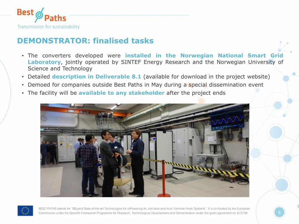
DEMONSTRATOR: finalised tasks
5
• Three MMC converters were designed from scratchfor Best Paths
• MMC with HB cells, 18 cells per arm
• MMC with FB cells, 12 cells per arm
• MMC with HB cells, 6 cells per arm
• During this year all the converter components havebeen built and successfully tested at full rating
• 42 modules
• 144 power cell boards
• 1764 capacitors
6
• The converters developed were installed in the Norwegian National Smart GridLaboratory, jointly operated by SINTEF Energy Research and the Norwegian University ofScience and Technology
• Detailed description in Deliverable 8.1 (available for download in the project website)
• Demoed for companies outside Best Paths in May during a special dissemination event
• The facility will be available to any stakeholder after the project ends
DEMONSTRATOR: finalised tasks

7
• The converters were commissioned in June with the collaboration of experts fromEnerginet
• Deliverable 8.2 will include the results of the tests carried out in the demonstrator, aswell as the report of the commissioning of the converters.
DEMONSTRATOR: finalised tasks
Conv12 700UDC, 100% active current Id (-81.2A) Phase C upper arm voltage, Phase C Lower arm voltage,
Phase C output voltage, Phase C arm current
Conv18 700UDC, 24.3kW,7.8kVar Phase C upper arm voltage, Phase C Lower arm voltage,
Phase C output voltage, Phase C arm current

DEMONSTRATOR: work in progress
8
• Gamesa’s WF model is being adapted to run in the 200 kVA high-bandwidth gridemulator that is available in the laboratory
• An improvement to the initial the scope: D8.2 will be updated with results at a later stagenext year
• Power Hardware in the Loop implementation combining the real time simulator and the gridemulator
Flexibility in the model simulated
Possibility to reproduce faster dynamics
IA
IB
IC
IA*
IB*
IC*
UA
UB
UC
Real Time Wind Farm Model UA*
UB*
UC*
Grid EmulatorReal Time Simulator
Current References
Voltage Measurements
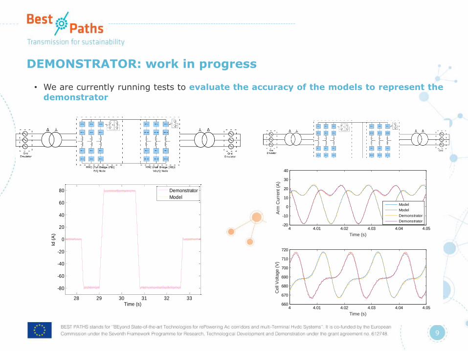
DEMONSTRATOR: work in progress
9
• We are currently running tests to evaluate the accuracy of the models to represent thedemonstrator
28 29 30 31 32 33
-80
-60
-40
-20
0
20
40
60
80
Time (s)
Id (
A)
Demonstrator
Model
4 4.01 4.02 4.03 4.04 4.05-20
-10
0
10
20
30
40
Time (s)
Arm
Curr
ent (A
)
Model
Model
Demonstrator
Demonstrator
4 4.01 4.02 4.03 4.04 4.05660
670
680
690
700
710
720
Time (s)
Cell
Voltage (
V)

DEMONSTRATOR: next steps
10
• Complete the matching of the models and demonstrator (November)
• Define the final tests to be carried out (November)
• Document results in D8.2 (December)

11
Max Parker, University of Strathclyde
12
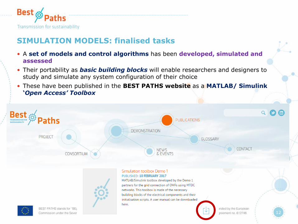
SIMULATION MODELS: finalised tasks
• A set of models and control algorithms has been developed, simulated and assessed
• Their portability as basic building blocks will enable researchers and designers to study and simulate any system configuration of their choice
• These have been published in the BEST PATHS website as a MATLAB/ Simulink ‘Open Access’ Toolbox

SIMULATION MODELS: finalised tasks
13
• The user manual comes with the published models and accompanying examples
• Specific blocks include models of:
o High level controllers
o Converter stations
o AC grid
o DC cables
o Wind farm
• Detailed descriptions available in Deliverable 3.1
SIMULATION MODELS: finalised tasks
14
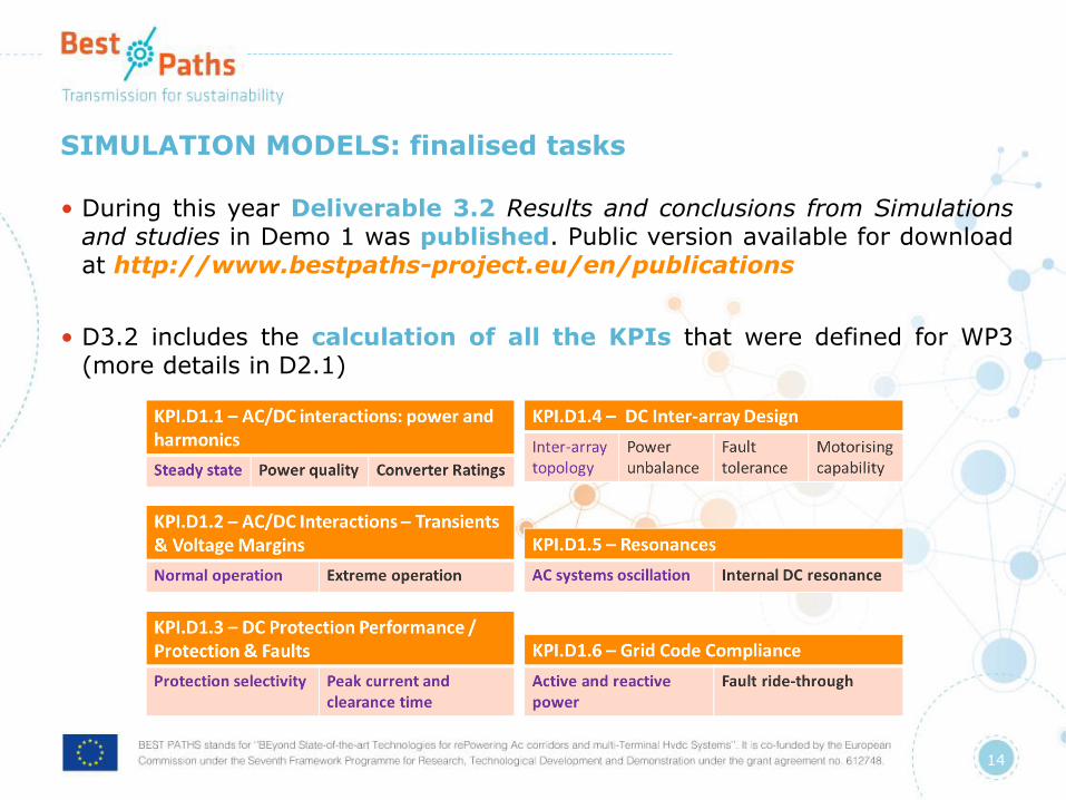
• During this year Deliverable 3.2 Results and conclusions from Simulationsand studies in Demo 1 was published. Public version available for downloadat http://www.bestpaths-project.eu/en/publications
• D3.2 includes the calculation of all the KPIs that were defined for WP3(more details in D2.1)
SIMULATION MODELS: finalised tasks
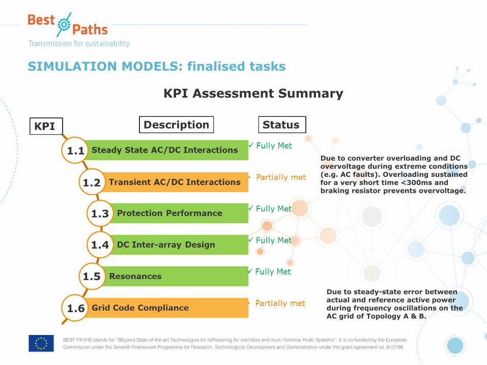
Due to converter overloading and DC overvoltage during extreme conditions (e.g. AC faults). Overloading sustained for a very short time <300ms and braking resistor prevents overvoltage.
Due to steady-state error between actual and reference active power during frequency oscillations on the AC grid of Topology A & B.
KPI Assessment Summary

SIMULATION MODELS: work in progress
16
• Matching of models and demonstrator
o Increases accuracy
o Real measurements compared against simulations
o Model parameters tweaked until results are as similar to themeasurements as possible
o Parameters to match:
Transformer magnetisation inductance and resistance
Transformer leakage inductance and copper resistance
• Nameplate values used
Cell capacitor ESR
• Small effect, chosen based on datasheet.
Arm Inductance
• Includes any parasitics
Arm Resistance
• Combined resistance of arm inductors, MOSFETs, PCBs, cables etc.
Controller delay
Voltage measurement delay (relative to current)

Matching of Transformer Parameters – estimated from open-circuit tests
Magnetising reactance:
𝑋𝑚 =3𝑉𝑝ℎ
2
𝑄𝑜𝑐
Results for 18-level:
Value for 330V used
Iron-loss resistance:
𝑅𝑚 =3𝑉𝑝ℎ
2
𝑃𝑜𝑐
17
0
50
100
150
200
250
300
0 100 200 300 400
Rm
PU
Vph (V)
23.5
24
24.5
25
25.5
26
26.5
27
27.5
0 100 200 300 400
Xm
PU
Vph (V)
SIMULATION MODELS: work in progress
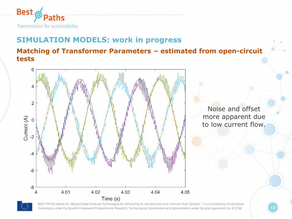
Noise and offset more apparent due to low current flow.
18
Matching of Transformer Parameters – estimated from open-circuit tests
SIMULATION MODELS: work in progress
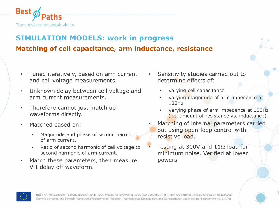
• Tuned iteratively, based on arm current and cell voltage measurements.
• Unknown delay between cell voltage and arm current measurements.
• Therefore cannot just match up waveforms directly.
• Matched based on:
• Magnitude and phase of second harmonic of arm current.
• Ratio of second harmonic of cell voltage to second harmonic of arm current.
• Match these parameters, then measure V-I delay off waveform.
• Sensitivity studies carried out to determine effects of:
• Varying cell capacitance
• Varying magnitude of arm impedence at 100Hz
• Varying phase of arm impedence at 100Hz (i.e. amount of resistance vs. inductance).
• Matching of internal parameters carried out using open-loop control with resistive load.
• Testing at 300V and 11Ω load for minimum noise. Verified at lower powers.
Matching of cell capacitance, arm inductance, resistance
SIMULATION MODELS: work in progress

0.4
0.5
0.6
0.7
0.8
0.9
1
1.1
1.2
1.3
1.4
0.7 0.8 0.9 1 1.1 1.2
Zarm Magnitude
I2/I1 I2/V2
20
Matching of arm inductance: effects of varying magnitude
SIMULATION MODELS: work in progress

21
0
0.1
0.2
0.3
0.4
0.5
0.6
0.7
0 2 4 6 8 10
I2 P
has
e
Zarm angle
Matching of arm inductance: effects of varying angle
SIMULATION MODELS: work in progress
22
0.6
0.7
0.8
0.9
1
1.1
1.2
1.3
1.4
1.5
1.6
0.017 0.019 0.021 0.023
Cell Capacitance (mF)
I2/I1 I2/V2
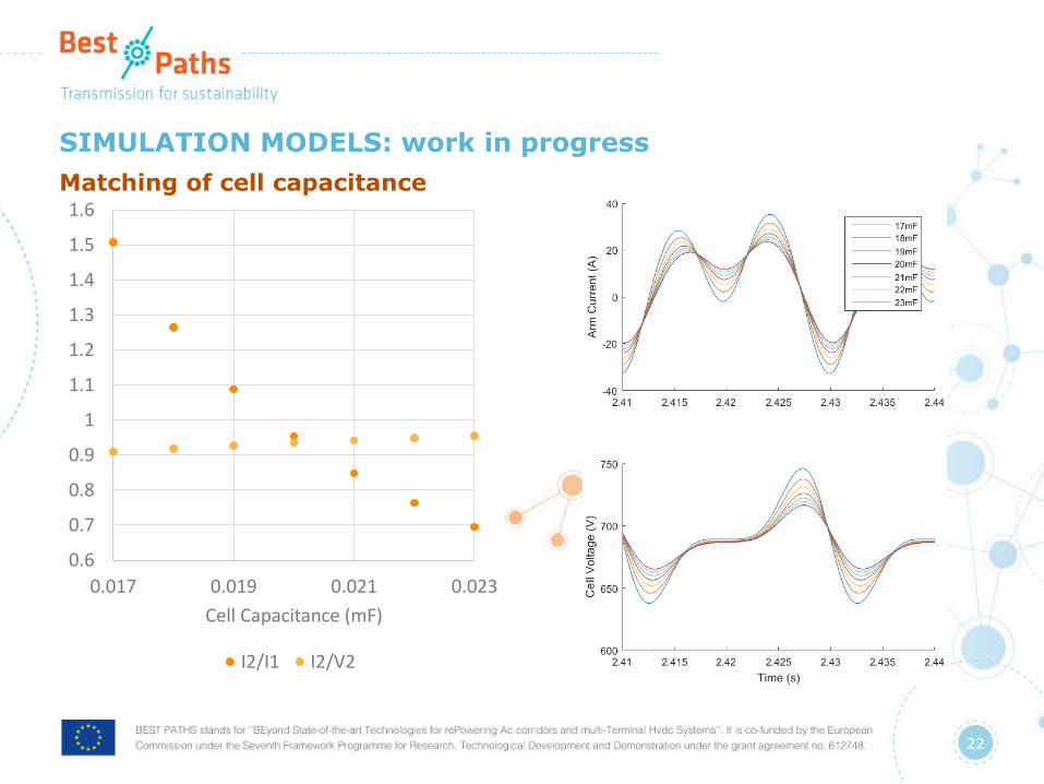
Matching of cell capacitance
SIMULATION MODELS: work in progress

23
Matching of voltage and current
SIMULATION MODELS: work in progress

24
Matching of arm current and cell voltage
SIMULATION MODELS: work in progress
25
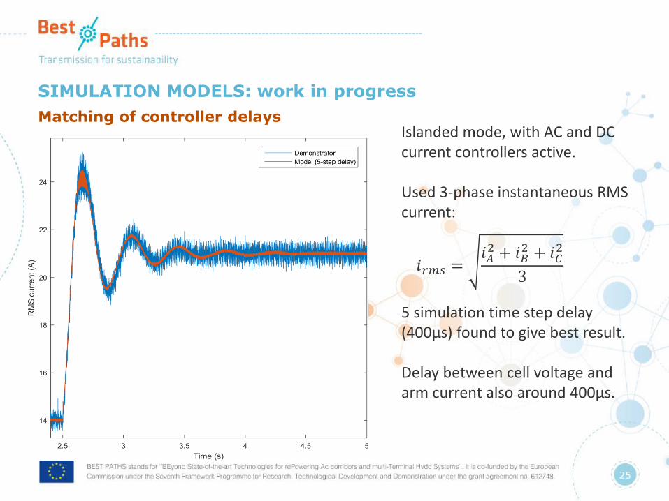
Islanded mode, with AC and DC current controllers active.
Used 3-phase instantaneous RMS current:
5 simulation time step delay (400µs) found to give best result.
Delay between cell voltage and arm current also around 400µs.
𝑖𝑟𝑚𝑠 =𝑖𝐴2 + 𝑖𝐵
2 + 𝑖𝐶2
3
Matching of controller delays
SIMULATION MODELS: work in progress

26
Matching of controller delays, non-islanded
SIMULATION MODELS: work in progress
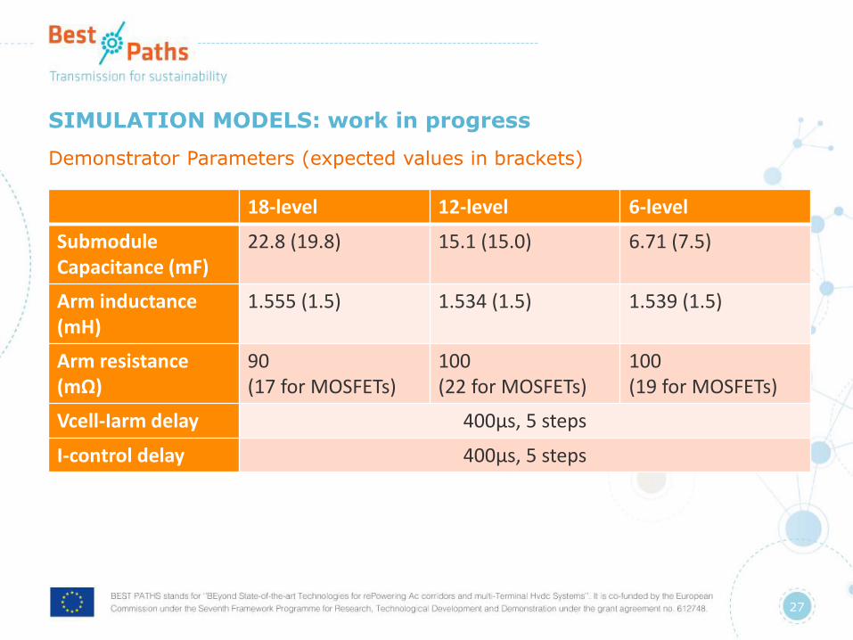
SIMULATION MODELS: work in progress
Demonstrator Parameters (expected values in brackets)
27
18-level 12-level 6-level
SubmoduleCapacitance (mF)
22.8 (19.8) 15.1 (15.0) 6.71 (7.5)
Arm inductance(mH)
1.555 (1.5) 1.534 (1.5) 1.539 (1.5)
Arm resistance(mΩ)
90(17 for MOSFETs)
100(22 for MOSFETs)
100(19 for MOSFETs)
Vcell-Iarm delay 400µs, 5 steps
I-control delay 400µs, 5 steps

THANK YOU!
QUESTIONS?
28