density functional theory and scanning...
TRANSCRIPT

DENSITY FUNCTIONAL THEORY AND SCANNING TRANSMISSION
ELECTRON MICROSCOPY:
SYNERGISTIC TOOLS FOR MATERIALS INVESTIGATION
By
Timothy John Pennycook
Dissertation
Submitted to the Faculty of the
Graduate School of Vanderbilt University
in partial fulfillment of the requirements
for the degree of
DOCTOR OF PHILOSOPHY
in
Physics
May 2012
Nashville, Tennessee
Approved:
Prof. Sokrates T. Pantelides
Dr. Maria Varela
Prof. Sandra J. Rosenthal
Prof. Kalman Varga
Dr. Mark P. Oxley

c© Copyright by Timothy John Pennycook 2012All Rights Reserved

ACKNOWLEDGEMENTS
This work was made possible through the support of many people. I am gratefulto all of them. In particular, I would like to thank Sokrates Pantelides for takingme as his student and for all the advise he has given me over the past five and ahalf years. Special thanks also go to Maria Varela for co-advising me and instructingme on the use of the microscopes. I am also grateful to the other members of myPhD committee, Mark Oxley, Kalman Varga and Sandra Rosenthal for their guidanceand collaboration. I would like to thank Matthew Beck and Juan Carlos Idrobo forteaching me how to perform density functional theory calculations and many valuablediscussions. I am also grateful to Oscar Restrepo and Weidong Luo for their adviceon density functional theory calculations. Thanks go to Juan Carlos Idrobo, MatthewChisholm, Andrew Lupini and William Sides for their aid and instruction in the useand maintenance of the microscopes. Thanks also go to Julia Luck for her instructionand assistance in the art of sample preparation. I am grateful to Jacobo Santamariaand his group for providing interesting samples and fruitful discussions. I thank JamesMcBride for all the help he has given me with the CdSe project, both growing samplesand working with me on the microscope. I thank George Hadjisavvas and PantelisKelires for collaborating with me on the Si nanocluster project. I thank OndrejKrivanek and the other members of Nion for their help, advise and collaboration.Finally, I would like to thank my father, Stephen Pennycook and the rest of the OakRidge National Laboratory STEM group for providing use of the microscope facilitiesand a great many constructive, as well as fun, discussions. This work was supported bythe US Department of Energy Grant DE-FG02-09ER46554 and the National ScienceFoundation GOALI under Grant No. DMR-0513048. Computations were performedat the National Energy Research Scientific Computing Center, which is supportedby the Office of Science of the U.S. Department of Energy under Contract No. DE-AC02-05CH11231.
iii

TABLE OF CONTENTS
Page
ACKNOWLEDGEMENTS . . . . . . . . . . . . . . . . . . . . . . . . . . . . iii
LIST OF TABLES . . . . . . . . . . . . . . . . . . . . . . . . . . . . . . . . . vi
LIST OF FIGURES . . . . . . . . . . . . . . . . . . . . . . . . . . . . . . . . vii
Chapter
I. INTRODUCTION . . . . . . . . . . . . . . . . . . . . . . . . . . . . 1
1.1. STEM . . . . . . . . . . . . . . . . . . . . . . . . . . . . . . 11.2. Density functional theory . . . . . . . . . . . . . . . . . . . 16
II. ALUMINA . . . . . . . . . . . . . . . . . . . . . . . . . . . . . . . . 28
III. COLOSSAL IONIC CONDUCTIVITY IN OXIDE MULTILAYERS . 33
IV. ATOM-BY-ATOM IDENTIFICATION OF ATOMS IN SINGLE LAYERBORON NITRIDEWITH ANNULAR DARK-FIELD STEM AND DFT 59
V. HYBRID DENSITY FUNCTIONAL THEORY APPLIED TO LCMO 66
VI. OPTICAL GAPS OF FREE AND EMBEDDED SI NANOCLUS-TERS: DENSITY FUNCTIONAL THEORY CALCULATIONS . . . 71
VII. WHITE LIGHT EMISSION FROMULTRASMALL CDSE NANOCRYS-TALS . . . . . . . . . . . . . . . . . . . . . . . . . . . . . . . . . . . 82
VIII. SUMMARY . . . . . . . . . . . . . . . . . . . . . . . . . . . . . . . . 93
iv

Appendicies
A. LIST OF REFEREED JOURNAL ARTICLES . . . . . . . . . . . . 96
1.1. Work Done as Part of This Thesis . . . . . . . . . . . . . . 961.2. Work Done in STEM as an Undergraduate . . . . . . . . . . 97
B. LIST OF TALKS AND POSTERS AT INTERNATIONAL MEETINGS 98
2.1. Talks . . . . . . . . . . . . . . . . . . . . . . . . . . . . . . . 982.2. Posters Presented During this Thesis . . . . . . . . . . . . . 992.3. Poster on STEM Presented as an Undergraduate . . . . . . 99
C. AWARDS . . . . . . . . . . . . . . . . . . . . . . . . . . . . . . . . . 100
3.1. Work Done as Part of This Thesis . . . . . . . . . . . . . . 1003.2. Work Done in STEM as an Undergraduate . . . . . . . . . . 100
REFERENCES . . . . . . . . . . . . . . . . . . . . . . . . . . . . . . . . . . . 101
v

LIST OF TABLES
Table Page
1.1. Naming conventions used to describe edges corresponding to transi-tions from different core states. . . . . . . . . . . . . . . . . . . . . 15
5.1. Energy difference between the AFM and FM magnetic orders ascalculated by HSE06. . . . . . . . . . . . . . . . . . . . . . . . . . . 70
vi

LIST OF FIGURES
Figure Page
1.1. As the probe is scanned across the sample the electrons scattered todifferent angles are collected by different detectors. In this schematicthe electrons scattered to low angles are collected by either a brightfield detector or a spectrometer. Those scattered out to higher anglesare collected by the annular dark field detector, the from which thesignal intensity is roughly proportional to the square of the atomicnumber Z, as illustrated in part (b) of the figure. . . . . . . . . . 2
1.2. Schematic showing the optics used to form the probe (a). The twolevels of scan coils work together to shift the beam across the samplewithout any net tilt (b). . . . . . . . . . . . . . . . . . . . . . . . 4
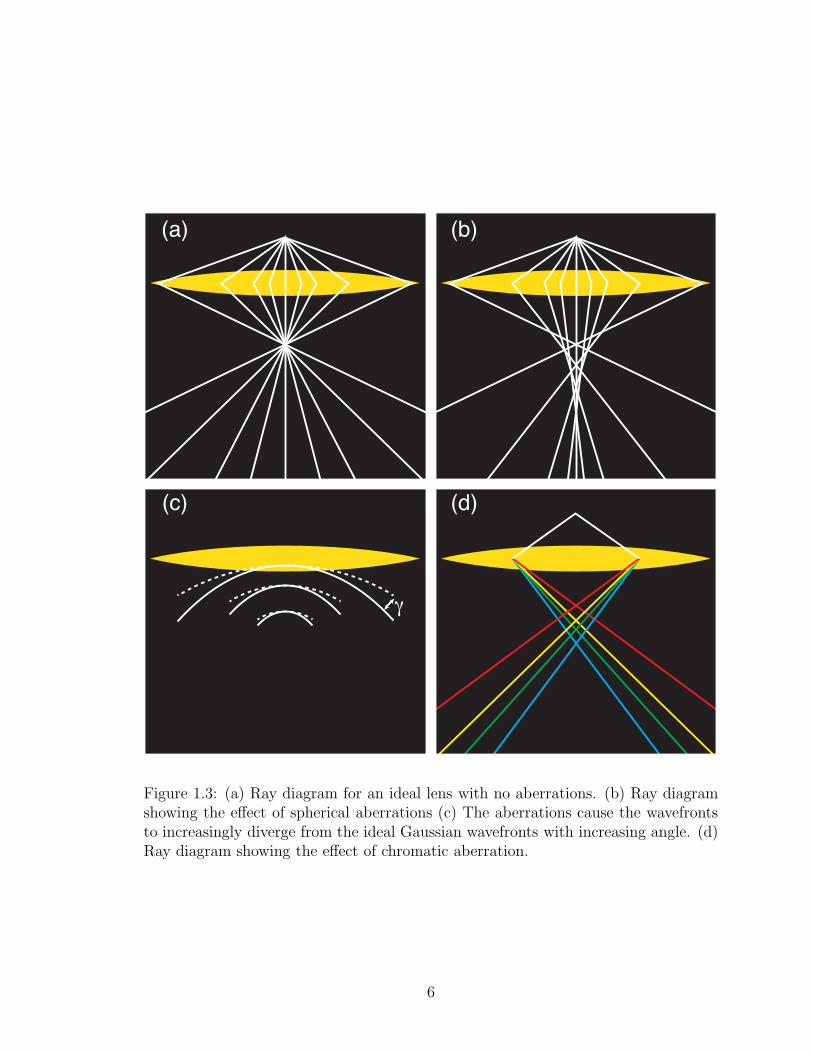
1.3. (a) Ray diagram for an ideal lens with no aberrations. (b) Ray dia-gram showing the effect of spherical aberrations (c) The aberrationscause the wavefronts to increasingly diverge from the ideal Gaus-sian wavefronts with increasing angle. (d) Ray diagram showing theeffect of chromatic aberration. . . . . . . . . . . . . . . . . . . . . 6
1.4. Diagrams displaying the relationship between the ideal and aber-rated wavefronts and rays. . . . . . . . . . . . . . . . . . . . . . . 8
1.5. Schematic of an EELS spectrum. . . . . . . . . . . . . . . . . . . . 12
1.6. Schematic demonstrating how EELS probes the unoccupied densityof states with electronic transitions from sharp core loss levels. Oc-cupied states are indicated with gray shading in the density of statesplot. Electronic transitions from the core levels to the empty con-duction band causes probe electrons to lose energy, resulting in theEELS spectrum on the right. . . . . . . . . . . . . . . . . . . . . . 13
1.7. Flow chart documenting the procedure for computing the total en-ergy of a material using DFT with a planewave basis. . . . . . . . . 24
1.8. Schematic comparing a pseudopotential to the full ionic potentialand the pseudowavefunction to the all-electron wavefunction as afunction of the distance from the center of the ion. . . . . . . . . . 27
2.1. Bulk HAl5O8 γ-alumina with a single substitutional Mg impurity.Mg atoms are shown in orange, Al in blue, O in red and H in white.The Mg Td position shown in (b) is 1.0 eV lower in energy than theOh position shown in (a). . . . . . . . . . . . . . . . . . . . . . . . 29
vii
2.2. Bulk HAl5O8 γ-alumina with a six Mg impurity atoms. The cluster-ing of Mg forming a pocket of Mg-spinel as shown in (a) is 0.3 eVlower in energy than the distribution shown in (a), indicating thatspinel nucleation is energetically favorable in the bulk. . . . . . . . 30
2.3. Moving a Mg atom from the subsurface Td position shown in (a)into the surface Oh position shown in (b) decreases the total energyby 0.3 eV. Moving it from the Oh site to the surface Td site shownin (c) decreases the energy a further 0.4 eV, making the surface Tdposition 0.7 eV more energetically favorable than the subsurface. . 30
2.4. The layer of spinel on top of the γ-alumina shown in (a) undergoesa major reconstruction into the structure shown in (b) when allowedto relax. Notice the tendency for Mg atoms to move into Oh sites. . 31
2.5. (a) Imaginary part of the dielectric function for bulk γ-HAl5O8, γ-Al2O3 and MgAl2O4. (b) Imaginary part of the dielectric functionfor bulk γ-HAl5+1/3O8, undoped and with 1% and 2% dopings of Mg. 32
3.1. Zirconia structures resulting from quantum mechanical simulatedannealing at various temperatures. O atoms are shown in red, andZr atoms in green. The 7% expansive strain is in the plane of thepage. The zig-zag ordering of the strained O sublattice shown at1000 K persists down to 0 K, but begins to break down at highertemperatures. At 2000 K and above the O positions appear random,in contrast to the unstrained material in which most O atoms simplyoscillate about the cubic-fluorite positions. . . . . . . . . . . . . . . 37
3.2. MSD of O atoms as a function of time during MD simulations atvarious temperatures. (Inset) Arrhenius plot of D from the strainedMSDs (same units). The linear fit shown in green yields an energybarrier of 0.4± 0.1 eV. . . . . . . . . . . . . . . . . . . . . . . . . 38
3.3. Structure of the 1 nm YSZ layer sandwiched between layers of STOat 360 K. Sr atoms are shown in yellow, Ti in blue, Zr in green, Yin gray, and O in red. . . . . . . . . . . . . . . . . . . . . . . . . . 39
3.4. Low magnification ADF images of YSZ/STO thin film multilayersacquired on a VG Microscopes HB501UX. (a) Sample showing flatcoherent multilayers grown in 2007. (b) Sample grown under slightlydifferent growth conditions in 2009 showing incoherent layers. . . . 43
viii

3.5. High resolution ADF images of islands of YSZ in STO are shownin (a) and (b). The arrow in (a) points to a section of coherentYSZ/STO. An elemental map created from a spectrum image of thethe area imaged in (b) is shown alongside a simultaneously acquiredADF image (c) in (d). Red, green and blue channels of (d) arecomposed of the integrated intensities of the O K, Zr M2,3 and M4,5,and Ti L2,3 edges respectively, causing STO to appear purple andYSZ yellow. . . . . . . . . . . . . . . . . . . . . . . . . . . . . . . 44
3.6. High resolution ADF images of sections of coherent regions of YSZ/STOmultilayers looking down the STO 〈100〉 and YSZ 〈110〉 directionsin (a) and the STO 〈110〉 and YSZ 〈100〉 in (b). ADF intensity isplotted as a function of position along the long direction of the redboxes for both images in the insets. The intensity is integrated alongthe direction of the short side of the red boxes. Blue arrows indicatethe transition from consistently high intensity peaks to alternatingbright dark peaks in the linetraces, corresponding to the transitionfrom YSZ to STO. The corresponding positions on the images arealso marked with arrows. . . . . . . . . . . . . . . . . . . . . . . . 45
3.7. (a) High resolution ADF image of a 〈100〉 YSZ layer sandwichedbetween 〈110〉 STO layers. A SI was acquired from the area indi-cated by the yellow rectangle superimposed on (a). An ADF imagerecorded simultaneously with the SI is shown in (b) at the samescale as the Ti elemental map shown in (c). A drop in the Ti inten-sity correlates with the more consistently bright columns of the YSZlayer. . . . . . . . . . . . . . . . . . . . . . . . . . . . . . . . . . . 47
3.8. EELS O K-edge fine structure simulated using DFT and the Z +1 approximation for bulk ordered cubic ZrO2 (shown in red) andthe 2000 K strained bulk structure with the extremely disordered Osublattice (shown in green). The energy loss is taken to be zero atthe Fermi energy. Both spectra were normalized to the intensitiesintegrated over the first 50 eV and broadened with a 0.5 eV Gaussian.It is seen that the disorder causes the fine structure to blur out. . 48
3.9. (a) O K-edge fine structure from the thin YSZ layer shown in Figure3.7 plotted in green and from bulk cubic YSZ in red. The multilayerspectrum was created from the same spectrum image used to pro-duce the Ti map in Figure 3.7. Pixels were summed up in the areacorresponding to the green box superimposed on the simultaneousADF image shown in (b). . . . . . . . . . . . . . . . . . . . . . . . 49
ix

3.10. (a) Model of YSZ/STO multilayer with ordered strained YSZ O sub-lattice viewed such that the STO is seen down the 〈110〉 direction.In this orientation the pure O columns of STO can be resolved usinghigh spatial resolution elemental mapping. The O columns of thestrained ordered YSZ have the same 2.76 A in plane separation asthe pure O columns in STO in the vertical direction of the Figureand a slightly shorter 2.39 A. As such, the YSZ O columns shouldbe resolved in an elemental map, if O atoms are ordered. If they areinstead disordered as in (b), then one would expect to see a highlyblurred out structure or just a blur. The blurring out is illustratedin (c) with a multislice simulation of the O K-edge elemental map ofthe structure shown in (b), viewed in the same orientation. The inte-grated intensity of each column of pixels in the simulated elementalmap is shown in (d). The intensity is shown in arbitrary units. . . 50
3.11. (a) High resolution ADF image of bulk YSZ viewed down the 〈100〉axis. A SI was acquired from the area indicated with the yellow boxsimultaneously with the ADF image shown in (b). The Zr M4,5 andO K edge integrated intensities of the PCA processed SI are shownas a function of position in (c) and (d) respectively. A composite ofthe two in which the red and green channels are composed of the Omap (making O intensity appear yellow) and the blue channel of theZr map is shown in (e). . . . . . . . . . . . . . . . . . . . . . . . . 51
3.12. (a) High resolution ADF image of a section of coherent YSZ/STOmultilayers viewed down the 〈110〉 STO axis. An ADF image recordedsimultaneously with a SI taken in the area indicated by the yellowbox is shown in (b). Integrated Ti L and O K edge intensity el-emental maps extracted from the PCA processed SI are shown in(c) and (d) and as a composite map in (e) in which O intensity isshown in yellow and Ti intensity is shown in blue. An O elementalmap extracted from the SI without PCA processing is shown in (f),and the integrated intensity of each row of pixels in the raw O mapis shown in (g). The intensity is given in arbitrary units, with thebackground subtracted to improve the contrast. . . . . . . . . . . . 53
3.13. (a) High resolution ADF image of an incoherent YSZ island sur-rounded by STO. (b) A magnified view of the interface on the leftside of the island shown in (a). The green lines are drawn throughthe centers of the Zr columns, illustrating the expansive strain thatoccurs in these regions near the interface. . . . . . . . . . . . . . . 55
x

3.14. (a) High resolution ADF image of an incoherent island of YSZ sur-rounded by STO. (b) ADF image recorded simultaneously with a SIrecorded in the area indicated by the yellow box in (a). Ti and Oelemental maps extracted from the SI are shown in (c) and (d) atthe same scale as (b). The O K-edge extracted from the regions indi-cated by the corresponding colors in (b) are shown in (e). The greenspectrum shows a significant reduction in the continuum region ofthe spectrum, indicating the presence of O vacancies. . . . . . . . 57
4.1. ADF STEM image of monolayer BN. (a), As recorded. (b), Cor-rected for distortion, smoothed, and deconvolved to remove probetail contributions to nearest neighbours. (c), Line profiles showingthe image intensity (normalized to equal one for a single boron atom)as a function of position in image b along X-X’ and Y-Y’. The el-ements giving rise to the peaks seen in the profiles are identifiedby their chemical symbols. Inset at top right in a shows the Fouriertransform of an image area away from the thicker regions. Its two ar-rows point to (1120) and (2020) reflections of the hexagonal BN thatcorrespond to recorded spacings of 1.26 and 1.09 A. Image recordedby M. F. Chisholm, deconvolution performed by O. L. Krivanek andN. Dellby. . . . . . . . . . . . . . . . . . . . . . . . . . . . . . . . 61
4.2. Analysis of image intensities. (a), Histogram of the intensities ofatomic image maxima in the monolayer area of Figure 4.1(b). (b),Plot of the average intensities of the different types of atoms versustheir atomic number, Z. The heights of the rectangles shown for B,C, N and O correspond to the experimental error in determining themean of each atomic types intensity distribution. . . . . . . . . . . 62
4.3. Part of a DFT simulation of a single BN layer containing the exper-imentally observed substitutional impurities overlaid on the corre-sponding part of the experimental image. Red, B; yellow, C; green,N; blue, O. . . . . . . . . . . . . . . . . . . . . . . . . . . . . . . . 63
5.1. The phase diagram of LaxCa1−xMnO3. . . . . . . . . . . . . . . . 67
5.2. The energy difference of the AFM and FM phases as a function of xin LaxCa1−xMnO3. The experimentally observed phase is indicatedin the colored bar at the top. . . . . . . . . . . . . . . . . . . . . . 67
5.3. The LMO supercell after relaxation with HSE06 (left) with an iso-lated oxygen octahedron with bond lengths labeled as used to de-scribe the Jahn-Teller distortions (right). . . . . . . . . . . . . . . 69
xi
6.1. TDLDA photoabsorption and the LDA DOS for the undeformed Si-NCs at various levels of oxidation. (a) has no O, (b) has one Obridge-bond, (c) has two O bridge-bonds, (d) has one O double-bond, (e) has one layer of oxide, and (f) has two layers of oxide.The corresponding TDLDA optical and LDA HOMO-LUMO gapsare indicated. . . . . . . . . . . . . . . . . . . . . . . . . . . . . . 75
6.2. TDLDA photoabsorption and the LDA DOS for the deformed Si-NCs at various levels of oxidation. (a) has no O, (b) has one Obridge-bond, (c) has two O bridge-bonds, (d) has one O double-bond, (e) has one layer of oxide, and (f) has two layers of oxide.The corresponding TDLDA optical and LDA HOMO-LUMO gapsare indicated. . . . . . . . . . . . . . . . . . . . . . . . . . . . . . 75
6.3. Charge density isosurfaces (dark blue) superimposed on the struc-tures of the undeformed (top) and deformed (bottom) Si-NCs with asingle O atom (dark/red) double bonded to their surfaces. Si atomsare shown as large gold balls and H as small light pink colored balls.The charge densities are weighted according to each state’s contri-bution to the TDLDA photoabsorption strength up to 4 eV for theundeformed structure and 3 eV for the deformed structure. Isosur-faces are plotted at 10% of the maximum charge density. . . . . . 76
6.4. Charge density isosurfaces (dark blue) superimposed on the struc-tures of the undeformed (top) and deformed (bottom) Si-NCs withtwo O (dark/red) atoms bridge bonded to their surfaces. Si atomsare shown as large gold balls and H as small light pink colored balls.The charge densities are weighted according to each state’s contri-bution to the TDLDA photoabsorption strength up to 5 eV for theundeformed structure and 4 eV for the deformed structure. Isosur-faces are plotted at 10% of the maximum charge density. . . . . . 77
6.5. Charge density isosurfaces (dark blue) superimposed on the struc-tures of the undeformed (top) and deformed (bottom) Si-NCs withtwo O atoms bridge bonded to their surfaces and covered in a fulllayer of SiO2. Si atoms are shown as large gold balls, O as smaller redballs and H as small light pink colored balls. The charge densitiesare weighted according to each state’s contribution to the TDLDAphotoabsorption strength up to 4 eV for the undeformed structureand 3 eV for the deformed structure. Isosurfaces are plotted at 10%of the maximum charge density. . . . . . . . . . . . . . . . . . . . 78
xii
7.1. Atomic resolution Z-contrast STEM images and optical emissionspectra from CdSe nanocrystals of 7 nm ((a) and (b)), 5 nm ((c)and (d)), and 3 nm ((e) and (f)) diameters. (g) White light spec-trum emitted by ultrasmall sub-2-nm CdSe nanoclusters. ((h) to(k)) Successive frames from a STEM movie showing the continuousmotion and disorder of the ultrasmall clusters. Scale bars are 1 nm. 85
7.2. Density functional simulations of ultrasmall CdSe. ((a) to (d)) Snap-shots from a 500 K quantum MD simulation of a Cd27Se27. (e) DOScalculated at 40 fs intervals during the 500 K simulation. The zeroof the bottom energy axis has been set to the DFT Fermi level. Thetop axis has been shifted 1.2 eV to account for the well known un-derestimation of the band gap by DFT. Each DOS has been coloredaccording to the energy of the lowest unoccupied state on this re-calibrated axis. (f) An emission spectrum simulated from 20 DOScalculated at intervals of 40 fs. . . . . . . . . . . . . . . . . . . . . 88
7.3. Charge density isosurfaces of the three highest occupied states ((a)to (c)) and three lowest unoccupied states ((d) to (f)) plotted forone of the Cd27Se27 structures produced during the 500 K moleculardynamics simulation. . . . . . . . . . . . . . . . . . . . . . . . . . 90
xiii

CHAPTER I
INTRODUCTION
The combination of density functional theory (DFT)[1, 2, 3, 4] and scanning trans-
mission electron microscopy (STEM)[5, 6, 7] provides a very powerful means of syn-
ergistic atomic-scale materials investigation. STEM provides simultaneous atomic
number contrast imaging [8, 9, 10, 11] and electron-energy loss spectroscopy (EELS)
[12, 13, 14, 15] with atomic-scale spatial resolution. DFT provides a means of perform-
ing accurate quantum mechanical calculations of many materials properties, which
are often difficult or impossible to probe experimentally. The strengths and limita-
tions of the two methods are truly complementary, enabling a cycle of theory and
experiment that self-consistently extends our knowledge of both practical materials
science and fundamental physics.
1.1 STEM
In STEM, an electron beam is focused into a small probe and scanned across
the sample as shown in Figure 1.1. The key advantage of the technique is that the
scattering of the probe electrons out to different angles can be recorded simultaneously
as a function of position. The most common configuration is to combine a large
annular detector with a small disk detector and a electron-energy loss spectrometer.
The annular detector typically detects scattering out to high angles while the small
disk detects scattering to low angles. As scattering to high angles occurs when the
probe is located over a strongly scattering object such as an atomic column, but not
in empty space, the annular detector is called the annular dark field (ADF) detector.
As empty space appears bright on the disk detector, it is called the bright field (BF)
detector.
As on a conventional transmission electron microscope (TEM), interpreting bright
1

(a) (b)
Annular dark field detector
Annular dark field image
Removable bright field detector
Spectrometer
Scanning Probe
Figure 1.1: As the probe is scanned across the sample the electrons scattered todifferent angles are collected by different detectors. In this schematic the electronsscattered to low angles are collected by either a bright field detector or a spectrometer.Those scattered out to higher angles are collected by the annular dark field detector,the from which the signal intensity is roughly proportional to the square of the atomicnumber Z, as illustrated in part (b) of the figure.
2

field images is nontrivial. Bright field images are coherent, the result of the inter-
ference of many diffracting beams. As a result, bright field image contrast depends
strongly on the sample thickness and the defocus of the electron beam. Atoms can
appear dark on a bright background or bright on a dark background, and everything
between. The images formed from the ADF detector on the other hand are mostly
incoherent, as are the images we typically see with our eyes, and therefore much more
easily interpreted. Atomic columns always appear bright on a dark background, with
an intensity roughly proportional to Z2 where Z is the atomic number of the con-
stituent atoms. This is illustrated in Figure 1.1(b) for SrTiO3 viewed down the 〈110〉
axis. The Z2 dependance arises because in order to scatter to high angles, the beam
electrons must pass very close to the nucleus of an atom where they undergo Ruther-
ford scattering, seeing essentially the full nuclear potential. In order to obtain a useful
signal, the inner detector angle is often reduced somewhat. The inclusion of signal
from lower angles reduces the exponent somewhat, but the Z dependance remains
strong. The reduction is caused by electrons scattered into lower angles seeing a
nuclear charge screened by atomic electrons. The relative ease of interpreting the
Z-contrast signal obtained from the high-angle ADF (HADF) detector makes it an
ideal reference when combined with simultaneously acquired EELS or BF images.
The formation of the electron probe starts with the acceleration of electrons from
an electron source. The much smaller wavelength of the electron is the reason why
the resolution of electron microscopes far exceeds that of optical microscopes. As
dictated by the de Broglie equation, the faster an electron travels, the smaller it’s
wavelength. Consequently, high voltages are used to accelerate the electrons. The
higher the accelerating voltage, the higher the resolution. Prior to the advent of aber-
ration correction, this led to the building of giant megavolt microscopes. Firing high
energy electrons at a sample, however, has a tendency to cause damage, and modern
microscopes typically operate between 60 and 300 kV. With aberration correction,
this range of voltages is sufficient to look at most samples with atomic resolution.
Resolutions of up to 0.5 A [16, 17] have been achieved at 300 kV. The Nion Ultra-
STEM 100 [18, 19, 20], with its fifth-order aberration corrector has a probe size just
3

ADF detector
BF detector
Spectrometer
Objective lensOptic axis
Scan Coils 1
Scan Coils 2
Probe forming apperture
Scan Coils
Condenser Lenses
Cold field emission tip
(a) (b)
Figure 1.2: Schematic showing the optics used to form the probe (a). The two levelsof scan coils work together to shift the beam across the sample without any net tilt(b).
4

over an Angstrom at 60 kV. The optimal accelerating voltage depends on whether the
specimen is more susceptible to knock-on or ionization damage. Knock-on damage, in
which atoms are knocked out of a specimen by the momentum of the beam electrons,
increases with with beam energy. Ionization damage, which results from electrons in
the sample absorbing enough energy from the beam to be ejected, actually decreases
with beam energy.
A number of electron sources can be used in the electron gun. Thermionic sources
use heat to push electrons over the work function energy barrier of the source material
and out into vacuum. Field emission sources use an electric field to pull electrons
out. Sharp points enhance electric fields. For example applying a voltage V to a
sphere with a radius of r produces an electric field E = V/r [21]. For this reason,
field emission sources use a very sharp needle, called a tip, as the emitter. In high-
resolution STEM the size of the scanned probe is determined by a combination of
the optics and the source. The optics produce a demagnified image of the source.
As it is easier to form a small probe from a small source, using a cold field-emission
gun (FEG) results in the best spatial resolution. Field emission requires a clean tip,
which can be achieved by keeping the gun at ultra-high vacuum and only periodically
heating the tip to remove any buildup of contamination. The need for ultra-high
vacuum makes designing and maintaining a cold FEG more difficult, but the benefits
are a considerably smaller source size and energy spread. For EELS, a cold FEG is
particularly desirable, as the energy spread of the source is what typically limits the
EELS energy resolution.
After being accelerated in the gun, the beam of electrons is demagnified by a set
of condenser lenses (Figure 1.2(a)). Two layers of of fast deflectors, called scanning
coils, allow the beam to be rastered across the sample. The first layer deflects the
beam to produce a shift. The second layer brings the beam back to parallel with the
optic axis, as illustrated in Figure 1.2(b). The final optical element involved in the
formation of the electron probe is the objective lens. It is the most powerful lens, and
does the largest amount of demagnification.
An ideal lens would put all rays from the same origin into focus at the same
5
(a) (b)
(d)
γ
(c)
Figure 1.3: (a) Ray diagram for an ideal lens with no aberrations. (b) Ray diagramshowing the effect of spherical aberrations (c) The aberrations cause the wavefrontsto increasingly diverge from the ideal Gaussian wavefronts with increasing angle. (d)Ray diagram showing the effect of chromatic aberration.
6
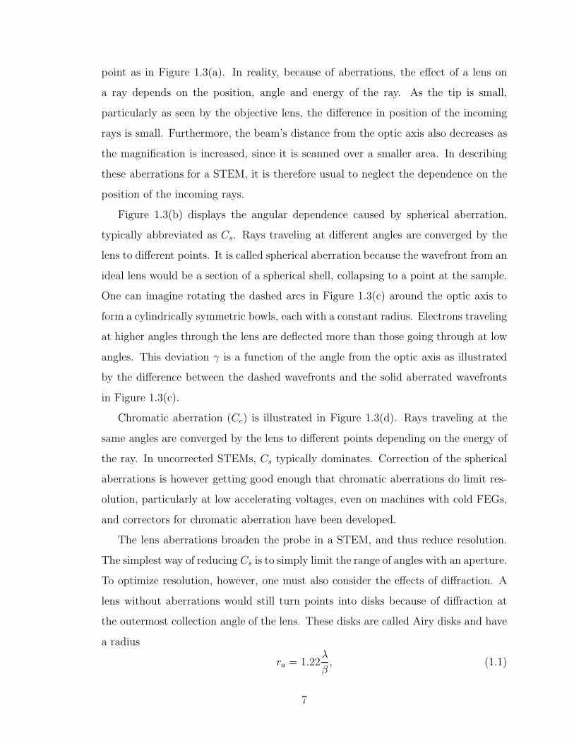
point as in Figure 1.3(a). In reality, because of aberrations, the effect of a lens on
a ray depends on the position, angle and energy of the ray. As the tip is small,
particularly as seen by the objective lens, the difference in position of the incoming
rays is small. Furthermore, the beam’s distance from the optic axis also decreases as
the magnification is increased, since it is scanned over a smaller area. In describing
these aberrations for a STEM, it is therefore usual to neglect the dependence on the
position of the incoming rays.
Figure 1.3(b) displays the angular dependence caused by spherical aberration,
typically abbreviated as Cs. Rays traveling at different angles are converged by the
lens to different points. It is called spherical aberration because the wavefront from an
ideal lens would be a section of a spherical shell, collapsing to a point at the sample.
One can imagine rotating the dashed arcs in Figure 1.3(c) around the optic axis to
form a cylindrically symmetric bowls, each with a constant radius. Electrons traveling
at higher angles through the lens are deflected more than those going through at low
angles. This deviation γ is a function of the angle from the optic axis as illustrated
by the difference between the dashed wavefronts and the solid aberrated wavefronts
in Figure 1.3(c).
Chromatic aberration (Cc) is illustrated in Figure 1.3(d). Rays traveling at the
same angles are converged by the lens to different points depending on the energy of
the ray. In uncorrected STEMs, Cs typically dominates. Correction of the spherical
aberrations is however getting good enough that chromatic aberrations do limit res-
olution, particularly at low accelerating voltages, even on machines with cold FEGs,
and correctors for chromatic aberration have been developed.
The lens aberrations broaden the probe in a STEM, and thus reduce resolution.
The simplest way of reducing Cs is to simply limit the range of angles with an aperture.
To optimize resolution, however, one must also consider the effects of diffraction. A
lens without aberrations would still turn points into disks because of diffraction at
the outermost collection angle of the lens. These disks are called Airy disks and have
a radius
ra = 1.22λ
β, (1.1)
7
where λ is the wavelength of the electron and β is the outermost semiangle of the
aperture. So while using a smaller aperture helps reduce the effects of aberrations,
it increases the diffraction limited resolution. The optimum aperture size is the one
that balances the competing effects of aberrations and diffraction.
Aberrated
wavefront
Aberrated
wavefront
Spherical
wavefront
Spherical
wavefront
γ
α
γ’γ
fdα
f
dγ
δ
δ
P
P’
A
A’
a b
Figure 1.4: Diagrams displaying the relationship between the ideal and aberratedwavefronts and rays.
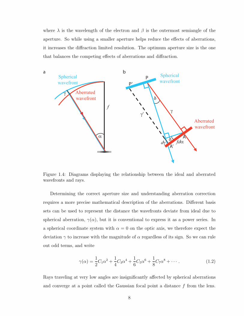
Determining the correct aperture size and understanding aberration correction
requires a more precise mathematical description of the aberrations. Different basis
sets can be used to represent the distance the wavefronts deviate from ideal due to
spherical aberration, γ(α), but it is conventional to express it as a power series. In
a spherical coordinate system with α = 0 on the optic axis, we therefore expect the
deviation γ to increase with the magnitude of α regardless of its sign. So we can rule
out odd terms, and write
γ(α) =1
2C1α
2 +1
4C3α
4 +1
6C5α
6 +1
8C7α
8 + · · · . (1.2)
Rays traveling at very low angles are insignificantly affected by spherical aberrations
and converge at a point called the Gaussian focal point a distance f from the lens.
8

Let ∆fa denote the distance from this point at which aberrated rays cross the optic
axis. The ratio of ∆fa to f in Figure 1.3(b) is exaggerated. In practice, ∆f ≪ f ,
and on the scale of viewing the whole path from the lens to the Gausian focal point,
the rays will appear to converge at the same point as in Figure 1.4(a). For small
α, the distance between the aberrated and spherical wavefronts will be very small
compared to f , so the difference between the lengths P-P’ and A-A’ in Figure 1.4(b)
will be negligible. In Figure 1.4(b) we have zoomed in very closely to the wavefronts
coming out the objective lens. An infinitesimal change in α increases length of γ by
an amount dγ. In this small angle approximation,
δ ≈ tan(δ) =1
f
dγ
dα, (1.3)
and thus the angle which the path of the ray deviates at the lens increases with α as
δ(α) = C1α + C3α3 + C5α
5 + C7α7 + · · · . (1.4)
C1 is just the distance the sample is from the Gaussian focal point of the lens δf . It can
be changed by either moving the sample up and down the optic axis or changing the
focal length of the lens with fine changes to the accelerating voltage or the lens current.
It is now clear why we use terms such as third order and fifth order aberrations when
speaking of aberration correction. Because α is small, the lowest order terms are the
most important.
The probe shape is determined by the superposition of all rays allowed through
the lens by the aperture. This can be though of as the interference of a set of plane
waves whose phase is modified by the aberrations. The so called aberration function
χ =2π
λγ = πδfλK2 +
π
2C3λ
3K
4 +π
3C5λ
5K
6 +π
4C7λ
7K
8 + · · · (1.5)
expresses the phase error they cause in terms of the transverse wave vector K which
has a magnitude K = α/λ. The probe amplitude can be expressed as a function of
9

position R in the plane a distance δf from the focal plane as
P (R) =
∫
A(K)e2πiK·Re−iχ(K)dK, (1.6)
where A(K) = 1 inside the aperture and zero outside. The intensity is just the square
I(R) = P 2(R) =
[∫
A(K)e2πiK·Re−iχ(K)dK
]2
. (1.7)
The diameter of the probe due to aberrations can be determined from this as a
function of defocus, which in turn can be used to determine the optimal aperture
size.
In 1949 Scherzer showed that for round lenses, the coefficients in the aberration
function, except defocus, are always positive [22]. He proved that, aside from using a
slight negative defocus, one couldn’t compensate higher order aberrations with rota-
tionally symmetric lenses. He demonstrated, however, that a set of non-rotationally
symmetric lenses could be employed to introduce negative aberrations and compen-
sate the positive aberrations of round lenses. Without such aberration correction,
Scherzer realized that microscopes in the 100-200 keV range would be limited to reso-
lutions of about 2 A. Scherzer even presented a design with which to compensate third
order spherical aberrations, and pointed out that if it were possible to control C3, it
would be best to make it negative in order to compensate fifth-order aberrations.
It would take half century for a successful corrector to be built and demonstrated.
It took so long because accurate correction requires a way to measure the aberra-
tions, and calculate the best way to counteract them. Before the availability of fast
computers and charged-coupled-device detectors, it was simply impossible to achieve
the necessary precision. Haider et al. demonstrated the first successful correction
of aberrations on a TEM using a hexapole corrector [23]. In 1998 Krivanek et al.
demonstrated the first successful implementation of a probe corrector for a STEM
the following year using a quadrupole/octupole design [24]. Following their initial
success, Ondrej Krivanek and Niklas Dellby founded the Nion company and began
10

working to improve their corrector design. In 2002 sub-A resolution was first demon-
strated in an electron microscope using a Nion corrector on a VG Microscopes HB501
STEM running at 120kV [25]. Putting a similar Nion corrector into the 300 kV VG
Microscopes HB603U pushed the resolution boundary down even further, allowing
the 0.78 A separation of Si 〈112〉 columns to be resolved [11].
The first aberration correctors all corrected up to third order aberrations. The
more terms in the aberration function that are counteracted, the more the aperture
can be opened up and the better the resolution. Soon after the success of the first
third-order correctors, designs for fifth-order correctors began to appear [26, 27].
Using fifth order correctors 0.68 A resolution was achieved in 2007 [28] and sub-
0.5 A was reached in 2009 [17, 29], all on 300 kV STEMs.
Fifth-order correction has also allowed lower kV beams to be used with atomic
resolution, which is very useful for materials with lower thresholds for knock-on dam-
age. Atomic resolution is now possible at 60 kV [20], and Z-contrast imaging has even
been used to identify all the atoms, including substitutional O and C impurities in
monolayer BN [19].
EELS also benefits from aberration correction. As with imaging, the finer probe
increases the spatial resolution at which EELS can be acquired. The negative defocus
used prior to aberration correction to increase image resolution also introduced large
probe tails, which could pick up the spectroscopic signal of atoms adjacent to the one
under the central peak of the probe [30]. Aberration correction mostly removes these
tails, facilitating the interpretation of spatially resolved EELS.
EELS probes the electronic structure of materials by measuring the distribution
of energies lost by the probe electrons. The distribution is divided into three regions.
They are the zero-loss, low-loss and core-loss regions as shown schematically in Figure
1.5. As the name suggests, zero-loss electrons have not undergone significant inelastic
scattering. TEM requires very thin samples, and usually the zero-loss peak is by far
the largest feature in an EELS spectrum. The width of the zero loss peak is a good
indicator of the energy resolution of the microscope, which is ideally limited only
by the energy spread of the emission source. After the zero loss, the next features
11

Energy Loss (a.u.)
zero-loss peak
low-loss
plasmon
band gap
core-loss
x106
Co
un
ts (
a.u
.)
core-loss edge
Figure 1.5: Schematic of an EELS spectrum.
12

En
erg
y
Density of States
core levels
e-
valence band
conduction band
Energy Loss (a.u.)
Inte
nsi
ty (
a.u
.)
ELNES EXELFS
Figure 1.6: Schematic demonstrating how EELS probes the unoccupied density ofstates with electronic transitions from sharp core loss levels. Occupied states areindicated with gray shading in the density of states plot. Electronic transitions fromthe core levels to the empty conduction band causes probe electrons to lose energy,resulting in the EELS spectrum on the right.
13

seen going up in energy loss are those corresponding to the lowest energy electronic
transitions in the material. If the material has a band gap, and the energy resolution
of the microscope is good enough, one can see it as a gap between the zero loss peak
and the next lowest energy features in the spectrum. Plasmons are also present in
the low loss region, and are typically the dominant features of the region. The ratio
of the zero-loss peak and the integrated plasmon energy-loss intensity gives a good
indication of the thickness of the sample.
Features with energy losses above 100 eV are typically core-loss in nature, corre-
sponding to transitions from core shell levels deep inside the atoms to the unoccupied
states above the Fermi level as illustrated in Figure 1.6. The spectroscopic features
produced by these transitions have a shape corresponding to the convolution of the
core levels with the unoccupied densities of states, modulated by the quantum me-
chanical rules governing electronic transitions. Because the shape tends to be more
complicated than a simple peak, the energy at which transitions from a given set of
core levels begins is called an edge. The term edge is also used to refer to all the
features coming from transitions from the same narrow set of core levels of the same
principle quantum number and orbital angular momentum. Edges corresponding to
transitions from core levels with principal quantum number n = 1, 2, 3, 4 are called K,
L, M and N edges respectfully. A numerical subscript is used to indicate the different
edges coming from the same quantum numbers. Core states with nonzero angular
momentum tend to be spit by the spin-orbit interaction. So, for instance, instead of
having just one edge from the 2p core levels (l = 1) we get two, one from the 2p1/2
(i.e. total angular momentum j = 1−1/2 = 1/2) which is called the L2 edge and one
from the 2p3/2 called the L3 edge. As the splitting is small on the scale of hundreds
of eV, it is common to refer to the EELS features from these split transitions as part
of the same edge. So one will often refer to the L2 and L3 edges collectively as the
L23 edge.
Each element has a different set of core levels giving rise to characteristic edges.
These presence of these edges can be used to identify the chemical identity of the
atoms in a material. With enough spatial localization of both the edge and the probe,
14

Table 1.1: Naming conventions used to describe edges corresponding to transitionsfrom different core states.
Core state Spectroscopic name1s K2s L1
2p1/2 and 2p3/2 L23
3s M1
3p1/2 and 3p3/2 M23
3d3/2 and 3d5/2 M45
4s N1
4p1/2 and 4p3/2 N23
4d3/2 and 4d5/2 N45
4d5/2 and 4d7/2 N67
the presence of different elements can be determined with atomic spatial resolution.
Although changes in the Fermi level due to being placed in different materials can
cause the exact energy of the core-loss edges to shift somewhat for an element, these
material dependent shifts are typically only a few electron-volts, small on the scale
of the typical separation of core-loss edges from different elements.
The fine structure of an EELS edge is divided into two regions as illustrated
in Figure 1.6. The lowest energy features form the energy loss near-edge structure
(ELNES), and are the most direct probe of the density of states and provides infor-
mation about the local bonding environment such as the type of coordination and the
valence. Further from the absorption edge threshold the effects of plural scattering
start to dominate. The features in this region are called extended energy loss fine
structure (EXELFS). Oscillations in the EXELFS caused by diffraction can also pro-
vide information about the crystalline structure, but the ELNES is the more direct
route to probing the electronic structure. Plural scattering is also responsible for the
background which goes as one over energy. The amount of plural scattering increases
with sample thickness. Because the probability of single scattering events does not
increase as quickly as it does for plural scattering, the thinner the sample, the better
the signal to noise ratios.
Good signal to noise ratios are especially important when performing spectrum
15

imaging. In a spectrum image, spectra are recorded as a function of position. Typ-
ically, the spectra are recorded in a rectangular grid creating a three-dimensional
data set of energy-loss intensity I(x, y, E), allowing the strength of any spectroscopic
features to be displayed as a function of position as an image. The most simple ap-
plication of spectrum imaging is just to map the presence of different elements as a
function of position. When this is done with a fine enough grid, it is possible to pro-
duce an atomic resolution spectrum image, separately resolving each type of atomic
column. Such chemical mapping can be very useful when Z-contrast imaging is in-
sufficient to determine the identity or location of all the atoms in a material. Light
elements are often very difficult to detect against a background of much heavier atoms
in ADF images. Dopants of similar Z to the host material can also be hard to identify
with ADF imaging. With EELS spectrum imaging, one can image light atoms and
dopants even when they are not apparent in the Z-contrast images. Furthermore, one
can quantify the changes in chemical composition with EELS, detecting, for instance,
non-stoichiometry and segregation. One can also map the changes in fine structure
with atomic resolution, and use this information to draw conclusions about the elec-
tronic structure and bonding environment as a function of position. Caution must be
used when interpreting spectrum images, however, as channeling and other dynamical
diffraction effects can complicate the spatial dependence of the EELS signal [31, 32].
It is best to compare with the results of image simulations including such effects to
avoid misinterpretation. Density functional theory simulations of fine structure can
also be used to compliment experimental results, and confirm interpretations of the
experimentally observed fine structure.
1.2 Density functional theory
The nanoworld is intrinsically quantum mechanical in nature. In order to truly
understand the diverse effects observed in complex nanoscale materials requires quan-
tum mechanical theories. DFT makes it possible to accurately calculate many of the
properties of complex solids and molecules from quantum mechanical first-principles.
It is said [4] that soon after Schrodinger’s equation for the electronic wavefunction
16

had been shown to work extraordinarily well for simple systems such as He and H2,
P. M. Dirac declared the field of chemistry to be finished, its content being entirely
encapsulated by Schrodinger’s equation. He is also said [4] to have recognized, how-
ever, that in the vast majority of cases the equation was far too complex to be solved.
By using the electron density as the fundamental variable rather than the many-
body wavefunction, DFT greatly simplifies the mathematical problem, allowing even
complex systems described by unit cells containing hundreds of atoms to be studied
quantum mechanically.
The time-independent Schrodinger’s equation is
Hψ = Eψ, (1.8)
where H is the Hamiltonian, ψ is the wavefunction and E is the energy of either an
excited or ground state. For a single particle, the Hamiltonian reads
H = −h2
2m∇2 + V (r). (1.9)
For a many-body system such as a crystal, the Hamiltonian is more complicated. If
we consider that each charged particle can feel the Coulomb force from from all the
others, the many body Schrodinger’s equation can be written (using Gaussian units)
HΨ = −h2
2m∇2Ψ+
N∑
i=1
N∑
j=i+1
ZiZJ
|ri − rj|Ψ = EΨ, (1.10)
where Ψ is the many-body wavefunction depending on the positions ri of allN charged
particles. One can see how the number of cross terms quickly increases with the
number of particles. Most systems of interest consist of too many electrons and ions
for an exact solution to be found. Even the most simple solids are too complex for
their wavefunctions to be solved for exactly with this equation and approximations
must be made.
The first approximation to be made is based on the fact that the ions are much
more massive than electrons. The electrons can therefore move far more quickly and
17
move into an instantaneous ground state for any given configuration of ions before
the ions have a chance to move significantly. This justifies the Born-Oppenheimer
approximation, in which the ions are kept fixed when calculating the wavefunction of a
system. The ions can later be moved, and the most energetically favorable structure
can be found by comparing the total energy of different configurations of ions in
the Born-Oppenheimer approximation. The approximation allows for a significant
simplification of the Hamiltonian. The electron-electron, ion-electron, and ion-ion
interactions can now be separated and the Hamiltonian written as
H = −h2
2me
∇2+1
4πǫ0
Ne∑
i=1
Ne∑
j=i+1
e2
|ri − rj|+
Ne∑
i=1
Ni∑
k
eZk
|ri − rk|+
Ni∑
k=1
Ni∑
l=k+1
ZkZl
|rk − rl|, (1.11)
where e is the charge of an electron, Ne is the number of electrons and Ni is the
number of ions. When determining the electronic degrees of freedom, the last term is
simply a constant. This is still a very difficult Hamiltonian to work with for systems
with more than a single electron, and further approximations are needed.
The most simple many body ansatz one could use to simplify matters is the
Hartree approximation which assumes the many electron wavefunction to be a linear
combination of orthonormal single particle wavefunctions:
Ψ = ψ1(r1)ψ2(r1) · · ·ψN (rN) (1.12)
Using this form with the Schrodinger equation gives the Hartree equations:
[
−h2
2me∇2 + Vions(ri) + V H
i (ri)
]
ψi = ǫiψi(r); V Hi (ri) =
∑
j 6=i
〈ψj |e2
|ri − rj||ψj〉,
(1.13)
which can be solved iteratively.
The Hartree approximation, however, ignores the fermionic nature of electrons.
In order to satisfy the Pauli exclusion principle, the many-body wavefunction must
be antisymmetric with respect to the exchange of any two electron positions. For
18

instance if we have electrons at positions r1 and r2, their wavefunction must satisfy
Ψ(r1, r2) = Ψ(r2, r1). (1.14)
Hartree-Fock theory achieves this antisymmetry by expressing the wavefunction as a
determinant of N orthonormal orbitals (ψi) as
Ψ(r1, r2, . . . , rN) =
∣
∣
∣
∣
∣
∣
∣
∣
∣
∣
∣
∣
ψ1(r1) ψ1(r2) · · · ψ1(rN)
ψ2(r1) ψ2(r2) · · · ψ2(rN)...
.... . .
...
ψN (r1) ψN(r2) · · · ψN (rN)
∣
∣
∣
∣
∣
∣
∣
∣
∣
∣
∣
∣
. (1.15)
Because of the antisymmetry of the determinant, this wavefunction satisfies the Pauli
exclusion principle For instance, in the two electron system
Ψ(r1, r2) =
∣
∣
∣
∣
∣
∣
ψ1(r1) ψ1(r2)
ψ2(r1) ψ2(r2)
∣
∣
∣
∣
∣
∣
= −
∣
∣
∣
∣
∣
∣
ψ1(r2) ψ1(r1)
ψ2(r2) ψ2(r1)
∣
∣
∣
∣
∣
∣
= −Ψ(r2, r1). (1.16)
Using the Hartree-Fock many body wavefunction and Schrodinger’s equation gives
the Hartree-Fock equations:
[
−h2
2me
∇2 + Vions(ri) +∑
j 6=i
〈ψj|e2
|ri − rj ||ψj〉
]
ψi −∑
j 6=i
〈ψj|e2
|ri − rj ||ψi〉ψj = ǫiψi(r).
(1.17)
These equations are the same as the Hartree equations except for the appearance of
the extra term
−∑
j 6=i
〈ψj|e2
|ri − rj ||ψi〉ψj. (1.18)
due to enforcing the behavior under exchange demanded by the Pauli exclusion prin-
ciple.
The Hartree-Fock method works perhaps surprisingly well considering the approx-
imations made. In the Hartree-Fock approximation, each electron sees the average
19
position of all the others, when they should be responding to the actual instanta-
neous location of the other electrons. In other words, the electron motions should
be correlated, and in Hartree-Fock, they are not, causing significant errors in total
energies. So called post-Hartree-Fock methods extend the method to include correla-
tion effects. Basic Hartree-Fock calculations, however, already scale poorly with the
number of electrons, and these post-Hartree-Fock methods scale even more poorly.
Density-functional theory provides a means of addressing the lack of correlations
with far less computational difficulty than Hartree-Fock. The underlying concept
is to work with the electron density n(r) rather than the many-body wavefunction
Ψ({ri}). Hohenberg and and Kohn first showed [1] that given an external potential
V (r), the groundstate density n(r) is unique to within an irrelevant additive constant.
Since the density
n(r) = N
∫
Ψ∗(r, r2, . . . , rN)Ψ(r, r2, . . . , rN)dr2 . . .drN (1.19)
the potential V1(r) corresponds to the groundstate Ψ1 and the energy
E1 = 〈Ψ1|H1|Ψ1〉 =
∫
V1(r)n(r)dr+ 〈Ψ1|T + U |Ψ1〉, (1.20)
where H1 = V1+T +U and T and U are the kinetic and electron-electron interaction
energy operators.
Suppose a second potential V2(r) not equal to V1(r) plus a constant with ground-
state Ψ2 6= eiφΨ1 produces the same density n(r). Then the energy of this second
groundstate would be
E2 = 〈Ψ2|H2|Ψ2〉 =
∫
V2(r)n(r)dr+ 〈Ψ2|T + U |Ψ2〉. (1.21)
Assuming non-degenerate wavefunctions, the Rayleigh-Ritz theorem implies that if
20

Ψ is the groundstate wavefunction for a Hamiltonian the energy of any other wave-
function used with this Hamiltonian will be higher:
E = 〈Ψ|H|Ψ〉 < 〈Ψ′|H|Ψ′〉 = E ′. (1.22)
Using this principle,
E1 < 〈Ψ2|H1|Ψ2〉 =
∫
V1(r)n(r)dr+ 〈Ψ2|T + U |Ψ2〉 (1.23)
= E2 +
∫
[V1(r)− V2(r)]n(r)dr (1.24)
and similarly
E2 < E1 +
∫
[V2(r)− V1(r)]n(r)dr, (1.25)
but then adding these two together results in the contradictory statement that
E1 + E2 < E1 + E2. (1.26)
Therefore, by reductivo ad absurdum there cannot be two potentials differing by more
than a constant giving the same density. The proof has been extended to also apply
to degenerate groundstates [33]. As the external potential uniquely determines the
wavefunction to within an irrelevant phase factor, the link between the density and
the potential also means the density determines the wavefunction.
Instead of directly solving the Schrodinger equation, one could arrive at the so-
lution by applying the Rayleigh-Ritz theorem and finding the wavefunction Ψ which
produces the smallest energy
E = 〈Ψ|H|Ψ〉. (1.27)
The wavefunction that does this will also be the solution to the Schrodinger equation,
Ψ. For the set of trial wave functions Ψαn that produce a density n(r), the minimum
energy for a given potential is
E[n(r)] = minα
[
〈Ψαn|H|Ψα
n〉]
=
∫
V (r)n(r) + F [n(r)] (1.28)
21

where
F [n(r)] = minα
(
〈Ψαn|T + U |Ψα
n〉)
(1.29)
is a universal functional of the density, requiring no explicit knowledge of V (r). The
ground state energy is then
E = minnE[n(r)] = min
n
{∫
V (r)n(r) + F [n(r)]
}
(1.30)
This implies that if such a universal functional F [n] could be found and written
without reference to the many-body wavefunction, one could find the exact total
energy of a system without actually calculating its many-body wavefunction. As
long as one can find the right density, one can obtain the total energy. This means
that it is possible to find the total energy using an auxiliary system of fictitious non-
interacting particles moving in an effective potential which reproduces the density of
the real many-body system. Kohn and Sham [2] developed a set of equations for just
such a set of auxiliary non-interacting quasi-electrons. They started by defining the
functional
F [n(r)] = Ts[r] +e2
2
∫
n(r)n(r′)
|n(r)drdr′ + Exc[n(r)] (1.31)
in which
Ts[r] =∑
i
〈ψi| −h2
2me∇2|ψi〉 (1.32)
is the kinetic energy of the single particle states and the last term Exc[n(r)] is called
the exchange-correlation energy functional. To find the energy minimizing density
they derived from this using the constraint that the total number of electrons is a
constant, the Euler-Lagrange equations
δE[n(r)] =
∫
δn(r)
{
Veff(r) +δ
δn(r)Ts[n(r)]|n(r)=n(r) − ǫ
}
dr = 0 (1.33)
where
Veff(r) = V (r) +
∫
n(r′)
|r− r′|dr′ + Vxc (1.34)
22

and the exchange-correlation potential
Vxc =δExc[n(r)]
δn(r). (1.35)
From the Euler-Lagrange equations they saw that the energy minimizing density is
found by self-consistently solving the single particle equations
[
−h2
2me∇2 + Veff(r)
]
ψi(r) = ǫiψi(r), (1.36)
with
n(r) =N∑
j=1
|ψj(r)|2, (1.37)
which are now known as the Kohn-Sham equations. Figure 1.7 presents a flow chart
showing how the Kohn-Sham equations are solved self-consistently with a planewave
basis.
If the exchange-correlation functional Exc[n(r)] were known exactly, it would be
possible to compute exact many-body total energies with this method. Unfortunately,
for most systems of interest, no exact form is known, and we must rely on approximate
functionals. One system for which the functional can be calculated precisely is the
homogenous electron gas. All the approximations in use today are based on the cal-
culation of the energy of the gas as a function of density. The simplest approximation
is the local-density approximation (LDA), in which Exc[n(r)] depends on the density
only locally. For an electron at point r it is equal to the exchange-correlation energy
for an electron in a homogeneous electron gas with the same density. The interaction
should however be nonlocal, so it is surprising the LDA works as well as it does. In an
effort to more accurately portray the exchange-correlation functional, a slightly less
local approximation called the generalized-gradient approximation (GGA) was devel-
oped. The GGA Exc[n(r)] depends not just on the density at r, but on it’s gradient
[34]. The GGA tends to improve the accuracy of DFT calculations somewhat, but
at some computational cost due to the extra complexity. Different parameterizations
of Exc[n(r)] are available, and improving it is an active area of research. Even with
23
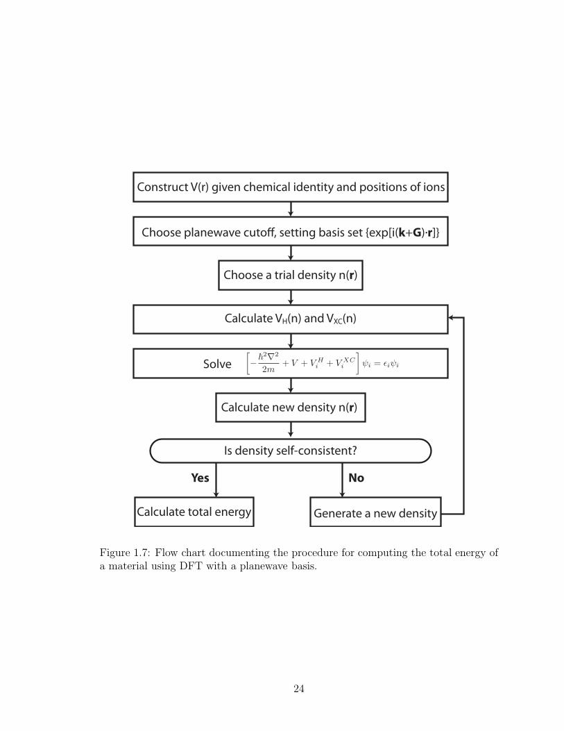
Construct V(r) given chemical identity and positions of ions
Choose planewave cuto!, setting basis set {exp[i(k+G).r]}
Choose a trial density n(r)
Calculate VH(n) and VXC(n)
Calculate new density n(r)
Solve
Calculate total energy Generate a new density
Is density self-consistent?
Yes No
Figure 1.7: Flow chart documenting the procedure for computing the total energy ofa material using DFT with a planewave basis.
24

these quite local approximations, DFT has provided a remarkably accurate means
of simulating materials quantum mechanically. Because of its computational cost ef-
fectiveness, it has opened the doors to understanding a plethora of materials which
would have otherwise been out of the reach of quantum mechanical simulations. The
value of DFT was recognized with the awarding of the Nobel prize to W. Kohn for
his work developing DFT and J. A. Pople for pioneering development of ab-initio
software using Gaussian basis sets.
The most natural basis set in which to set about solving the Kohn-Sham equations
for crystals is a plane wave basis. From Bloch’s theorem the wavefunctions of a crystal
can be written as the product of a cell-periodic function and a plane wave
ψi = exp(ik · r)fi(r). (1.38)
The cell-periodic function can be expanded as a series of plane waves
fi(r) =∑
G
ci,G exp(iG · r) (1.39)
in which theG vectors are reciprocal lattice vectors. So we can write the wavefunction
as a sum of plane waves
ψi(r) =∑
G
ci,k+G exp(i(k+G) · r) (1.40)
Only certain values of k are allowed by the periodic boundary conditions, however
there are an infinite number of these allowed “k-points”. The infinitely large number
of electrons in a crystal are accounted for by a finite set of electronic states at an
infinite number of k-points. Fortunately, wavefunctions are very similar at nearby k,
and a wavefunction at single k-point can be used to well represent the wavefunctions
over a whole region of k-space. Methods have also been devised to take advantage of
symmetry making it possible to use only a small set of special k-points to provide an
accurate representation [35]. In a real DFT calculation, convergence must be achieved
with respect to the number of k-points.
25
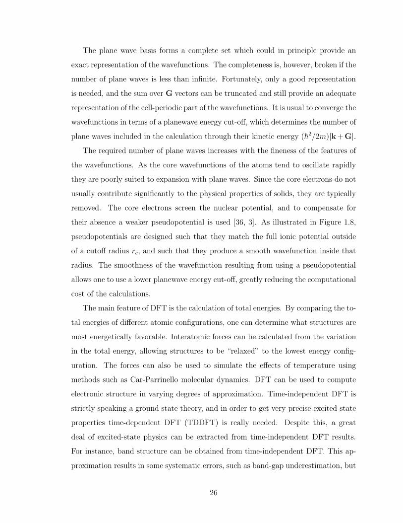
The plane wave basis forms a complete set which could in principle provide an
exact representation of the wavefunctions. The completeness is, however, broken if the
number of plane waves is less than infinite. Fortunately, only a good representation
is needed, and the sum over G vectors can be truncated and still provide an adequate
representation of the cell-periodic part of the wavefunctions. It is usual to converge the
wavefunctions in terms of a planewave energy cut-off, which determines the number of
plane waves included in the calculation through their kinetic energy (h2/2m)|k+G|.
The required number of plane waves increases with the fineness of the features of
the wavefunctions. As the core wavefunctions of the atoms tend to oscillate rapidly
they are poorly suited to expansion with plane waves. Since the core electrons do not
usually contribute significantly to the physical properties of solids, they are typically
removed. The core electrons screen the nuclear potential, and to compensate for
their absence a weaker pseudopotential is used [36, 3]. As illustrated in Figure 1.8,
pseudopotentials are designed such that they match the full ionic potential outside
of a cutoff radius rc, and such that they produce a smooth wavefunction inside that
radius. The smoothness of the wavefunction resulting from using a pseudopotential
allows one to use a lower planewave energy cut-off, greatly reducing the computational
cost of the calculations.
The main feature of DFT is the calculation of total energies. By comparing the to-
tal energies of different atomic configurations, one can determine what structures are
most energetically favorable. Interatomic forces can be calculated from the variation
in the total energy, allowing structures to be “relaxed” to the lowest energy config-
uration. The forces can also be used to simulate the effects of temperature using
methods such as Car-Parrinello molecular dynamics. DFT can be used to compute
electronic structure in varying degrees of approximation. Time-independent DFT is
strictly speaking a ground state theory, and in order to get very precise excited state
properties time-dependent DFT (TDDFT) is really needed. Despite this, a great
deal of excited-state physics can be extracted from time-independent DFT results.
For instance, band structure can be obtained from time-independent DFT. This ap-
proximation results in some systematic errors, such as band-gap underestimation, but
26

rrc
Vpsuedo
Z/r
Ψpsuedo
Ψfp
Figure 1.8: Schematic comparing a pseudopotential to the full ionic potential andthe pseudowavefunction to the all-electron wavefunction as a function of the distancefrom the center of the ion.
when these are kept in mind the results are still very useful. Optical properties and
EELS fine structure can be extracted as well. Both are more accurately simulated
using TDDFT, but time-independent DFT is simpler and less computationally de-
manding. These features allow DFT to be used to interpret what is observed in the
microscope and to make predictions that can then be tested by looking at the real
material with STEM, or other methods. The ensuing chapters will provide examples
of using DFT and STEM to investigate and uncover the mysteries of materials.
27

CHAPTER II
ALUMINA
I started my DFT work with a project exploring the effects of Mg on the structure
and optical properties of γ-Al2O3. The project was selected primarily to acquire
experiance with total energy calculations, optimization with defect configurations and
optical absorption spectra. A layer of alumina typically forms on aluminum surfaces,
either naturally or intentionally by anodization. Although pure alumina is transparent
in the visual range, the presence of impurities can cause it to become optically active.
Mg is commonly used as an alloying element in heat-treated aluminum alloys. If
Mg makes its way into the alumina surface layer, the appearance of the alloy can
be affected. The presence of Mg in γ-alumina has been reported to cause darkening,
mottling, and surface roughness [37, 38, 39, 40].
The γ-alumina structure is based on that of magnesium spinel (MgAl2O4). In
spinel, Mg atoms occupy tetrahedral (Td) sites, and Al atoms occupy octahedral (Oh)
sites. In γ-alumina, Al atoms occupy both Td and Oh positions, but in order to
satisfy the stoichiometry of Al2O3, 11% of the sites are left vacant. These built in
vacancies cause the alumina to act as a sponge for hydrogen [41], soaking up hydrogen
when exposed to the atmosphere. Since I wished to simulate the material as exposed
to the atmosphere, I performed our structural investigations with the lowest energy
H-containing stoichometry, HAl5O8 [41].
I started by posing the following questions: Given that the γ-alumina structure
is based on that of spinel, do dispersed Mg atoms occupy Td sites in γ-alumina as in
spinel, or are the Oh sites preferred, as in MgO? If Mg is present in the alumina will it
stay dispersed, or will it aggregate in the bulk or on the surface? I constructed a 1 x 2
x 2 supercell based on one of the minimum volume γ-alumina unit cells [42], such that
a single Mg atom placed in the supercell could be considered isolated. Performing
structural relaxations, I found that the total energy was lower by 1.0 eV when the Mg
atom was substituted for a Td Al atom rather than an Oh Al atom (see Figure 2.1).
28

I then introduced two additional Td Mg, spreading them far away from each other
initially, then bringing them together one at a time into nearest neighbor Td sites. A
tenth of an eV was gained by moving one of the Mg atoms next to another, which
was then lost when the third was brought in. However, having 6 Td Mg together
turns out to be 0.3 eV lower in energy than the configuration where they are evenly
distributed throughout the supercell (Figure 2.2), suggesting that spinel nucleation
is likely to occur under the right conditions.
Figure 2.1: Bulk HAl5O8 γ-alumina with a single substitutional Mg impurity. Mgatoms are shown in orange, Al in blue, O in red and H in white. The Mg Td positionshown in (b) is 1.0 eV lower in energy than the Oh position shown in (a).
I then shifted my focus to the surface region. A supercell with the preferentially
exposed (110)C surface [43, 44] was constructed with 10 Angstroms of vacuum. I
found that the total energy was reduced by 0.3 eV when an isolated Mg atom was
moved from a subsurface Td site to a surface Oh site as shown in Figure 2.3. Moving
the Mg atom to a surface Td site resulted in an additional 0.4 eV reduction in total
energy, suggesting that Mg impurities would migrate to the surface Td sites.
To further study the migration of Mg atoms to the surface, I introduced additional
Mg atoms into the subsurface region. Moving them to the surface one at a time, I
found that migration to the surface was favored energetically until the surface Td
sites were half saturated with Mg. After this point, the Mg atoms preferred to stay
in the subsurface. Unlike in the bulk, spinel nucleation at the surface therefore seems
29
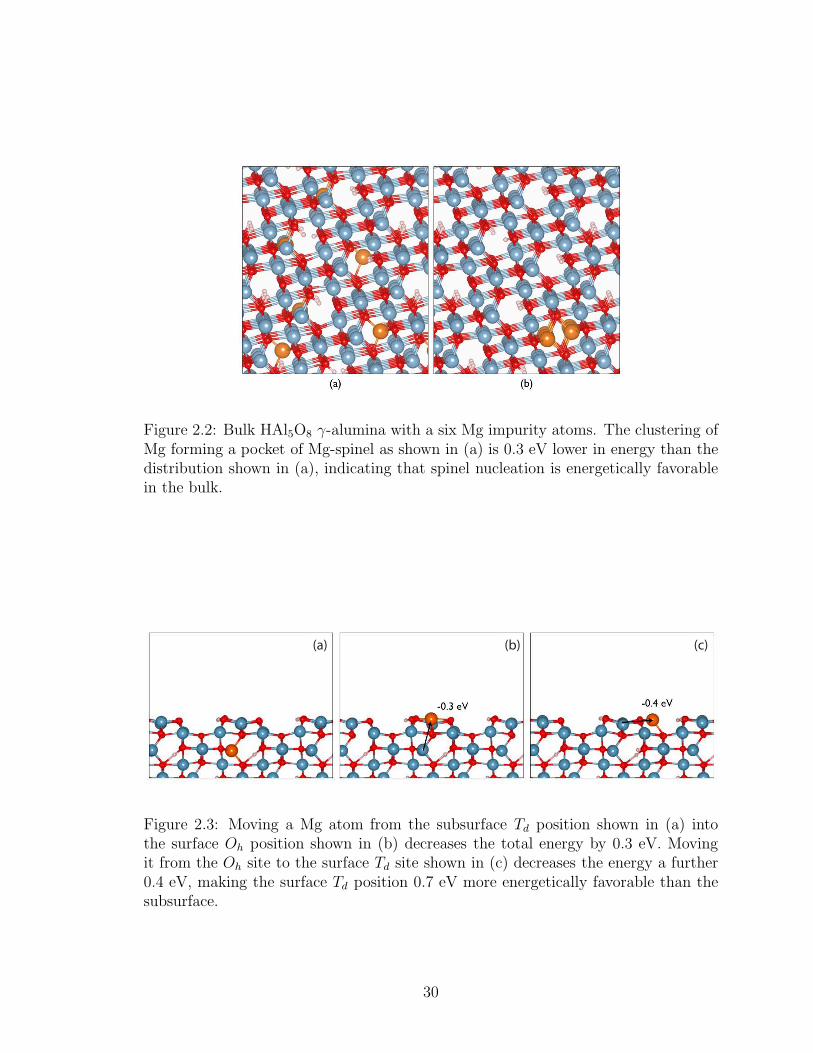
Figure 2.2: Bulk HAl5O8 γ-alumina with a six Mg impurity atoms. The clustering ofMg forming a pocket of Mg-spinel as shown in (a) is 0.3 eV lower in energy than thedistribution shown in (a), indicating that spinel nucleation is energetically favorablein the bulk.
(a) (b) (c)
Figure 2.3: Moving a Mg atom from the subsurface Td position shown in (a) intothe surface Oh position shown in (b) decreases the total energy by 0.3 eV. Movingit from the Oh site to the surface Td site shown in (c) decreases the energy a further0.4 eV, making the surface Td position 0.7 eV more energetically favorable than thesubsurface.
30
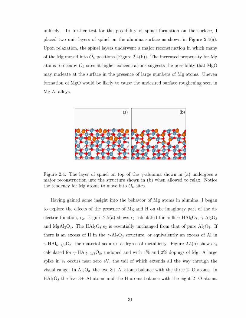
unlikely. To further test for the possibility of spinel formation on the surface, I
placed two unit layers of spinel on the alumina surface as shown in Figure 2.4(a).
Upon relaxation, the spinel layers underwent a major reconstruction in which many
of the Mg moved into Oh positions (Figure 2.4(b)). The increased propensity for Mg
atoms to occupy Oh sites at higher concentrations suggests the possibility that MgO
may nucleate at the surface in the presence of large numbers of Mg atoms. Uneven
formation of MgO would be likely to cause the undesired surface roughening seen in
Mg-Al alloys.
(a) (b)
Figure 2.4: The layer of spinel on top of the γ-alumina shown in (a) undergoes amajor reconstruction into the structure shown in (b) when allowed to relax. Noticethe tendency for Mg atoms to move into Oh sites.
Having gained some insight into the behavior of Mg atoms in alumina, I began
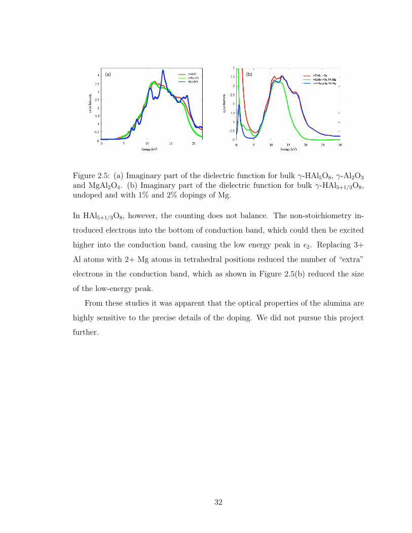
to explore the effects of the presence of Mg and H on the imaginary part of the di-
electric function, ǫ2. Figure 2.5(a) shows ǫ2 calculated for bulk γ-HAl5O8, γ-Al2O3
and MgAl2O4. The HAl5O8 ǫ2 is essentially unchanged from that of pure Al2O3. If
there is an excess of H in the γ-Al2O3 structure, or equivalently an excess of Al in
γ-HAl5+1/3O8, the material acquires a degree of metallicity. Figure 2.5(b) shows ǫ2
calculated for γ-HAl5+1/3O8, undoped and with 1% and 2% dopings of Mg. A large
spike in ǫ2 occurs near zero eV, the tail of which extends all the way through the
visual range. In Al2O3, the two 3+ Al atoms balance with the three 2- O atoms. In
HAl5O8 the five 3+ Al atoms and the H atoms balance with the eight 2- O atoms.
31
(a) (b)
Figure 2.5: (a) Imaginary part of the dielectric function for bulk γ-HAl5O8, γ-Al2O3
and MgAl2O4. (b) Imaginary part of the dielectric function for bulk γ-HAl5+1/3O8,undoped and with 1% and 2% dopings of Mg.
In HAl5+1/3O8, however, the counting does not balance. The non-stoichiometry in-
troduced electrons into the bottom of conduction band, which could then be excited
higher into the conduction band, causing the low energy peak in ǫ2. Replacing 3+
Al atoms with 2+ Mg atoms in tetrahedral positions reduced the number of “extra”
electrons in the conduction band, which as shown in Figure 2.5(b) reduced the size
of the low-energy peak.
From these studies it was apparent that the optical properties of the alumina are
highly sensitive to the precise details of the doping. We did not pursue this project
further.
32
CHAPTER III
COLOSSAL IONIC CONDUCTIVITY IN OXIDE MULTILAYERS
Ionic conductivity is essential to the operation of fuel cells and sensors. In a H
fuel cell, O and H are supplied separately to an anode and cathode that are separated
by an electrically insulating electrolyte ionic conductor. Chemical reactions occur
that release electrons at the anode and consume electrons at the cathode, resulting
in an electric potential difference which can be tapped to provide power. The role
of the ionic conductor is to permit either H or O ions, depending on the type of
fuel cell, to travel between anode and cathode so that they may react to form H2O.
As the rate at which fuel is delivered is limited by the ionic conductivity of the
electrolyte, so too is the current output of the fuel cell. In solid oxide fuel cells
(SOFCs), O2 is reduced to O ions at the cathode, which are transported though
a solid oxide electrolyte to the anode, where they react with H to form water and
electrons. SOFCs are among the most efficient types of fuel cells, but typically require
very high operating temperatures in order for their electrolytes to achieve sufficient
levels of ionic conductivity. The most commonly used O conducting electrolyte is
yttria stabilized zirconia (Y2O3)x(ZrO2)1−x (YSZ). It typically reaches usable levels
of ionic conductivity only at temperatures in excess of 700◦ C [45, 46, 47, 48]. Such
high temperatures tend to reduce durability, increase costs, and generally limit their
application. As a result, the search has been on for alternative O electrolytes with
higher ionic conductivities at lower temperatures.
Although progress has been made towards the goal of higher O ionic conductivites
at lower temperatures in bulk materials such as Ce1−xMxO2−δ (M: Sm, Gd, Ca, Mn),
the greatest enhancements have been achieved in heterogenous superlattices. Fol-
lowing work in CaF2-BaF2 multilayers [49, 50], which showed an increase in the F
ionic conductivity as the layer thickness was decreased, a variety of thin oxide het-
erostructures were fabricated. Enhancements of one to two orders of magnitude were
achieved in (YSZ + 8.7 mol. % CaO)/Y2O3 [51] and YSZ/Y2O3 [52] multilayers and
33
over three orders of magnitude in highly textured YSZ thin films grown on an MgO
substrate [53]. In these multilayer materials, the conductivity increased as the film
thicknesses were decreased or when the number of interfaces was increased, indica-
tive of an interfacial conduction pathway. It was proposed that in addition to space
charge effects, the disordered and partially coherent interfaces of these multilayers en-
hanced the ionic conductivities by opening up pathways of decreased packing density
[51, 52]. On the other hand, segregation in disordered areas such as grain boundaries
oriented perpendicular to the O ion current could also block O transport. The lack
of such blocking grain boundaries was attributed to the extra order of magnitude
enhancement of ionic conductivity in YSZ grown on MgO [53, 54].
Two primary mechanisms have typically been invoked to account for large, so-
called superionic conductivities. In the first case, there is a vacant sublattice that is
unavailable to the mobile ion at low temperatures. As the temperature is increased,
ions transfer randomly to the vacant sublattice and, at some critical temperature, an
order-disorder phase transition sets in leading to a highly conducting disordered phase
[55, 56]. This mechanism is often referred to as “sublattice melting”. In the second
case, ionic conduction is merely diffusion by the vacancy-mediated mechanism, i.e.,
vacancy hopping [57, 56]. In the case of YSZ, instead of relying solely on temperature
to produce vacancies, a supply of O vacancies results from replacing ZrO2 units with
Y2O3 units in the cubic fluorite lattice.
The greatest enhancements in O ionic conductivity were achieved by J. Santa-
maria and coworkers in YSZ/STO heterostructures [58]. The ionic conductivity of
the 8 mol % yttria YSZ in these heterostructures was measured to be up to eight or-
ders of magnitude higher than bulk YSZ between room temperature and 600 K. The
magnitude of the enhancement led to the effect being dubbed colossal ionic conduc-
tivity. The conductivity increased with the number of interfaces, but only slowly with
the YSZ layer thickness up to 30 nm, suggesting that the majority of O conduction
was occurring in the interface region.
The STEM images and x-ray experiments reported by Garcia-Barriocanal et al.
34

[58] showed the YSZ/STO interfaces possessing colossal ionic conductivity to be co-
herent and atomically flat, with the YSZ rotating 45◦ around the c axis and expanding
7% in-plane such that the two cation sublattices fit together perfectly. Although small
strains had been shown to enhance the diffusion of O ions in molecular dynamics simu-
lations of YSZ [59], it was previously thought that disorder would provide the greater
enhancement [51, 52]. Strains as large as 7% had not, however, been considered.
Based on lattice mismatch theory [60], one would not expect such large strains to be
stable, yet Santamaria’s group had produced coherent YSZ/STO interfaces despite
the 7% mismatch. A coherent expansively strained material has the advantage of
possessing a decreased packing density without the blocking effects of segregation or
grain boundaries.
Using DFT simulations I found that colossal ionic conductivity can be explained
in terms of a combination of lattice-mismatch strain and O sublattice incompatibility
as follows: Using finite temperature dynamical simulations of bulk cubic zirconia
with a built-in supply of O vacancies, I found that 7% strain completely changes
the O sublattice. At high temperatures the oxygen structure becomes extremely
disordered, so much so that by 2000 K the O sublattice appears completely random.
At these high temperatures, the mean-square-displacement (MSD), and therefore
the mobility, of the O atoms in the strained structure are greatly enhanced over
the already superionic unstrained structure. The enhancement correlates with the
degree of O disorder, but is not mediated by sublattice melting as no enhancement is
observed without vacancies. The key to understanding the low-temperature colossal
ionic conductivity lies in the finding that the incompatibility of the oxygen sublattices
at the YSZ-STO interface, together with the 7% lattice-mismatch strain, cause an
extreme O sublattice disorder at room temperature that is comparable to the disorder
found in strained bulk vacancy-doped zirconia at 2000 K. It was therefore possible
to use the high-temperature data to estimate the low-temperature conductivity of
the strained multilayers to be greater than 106 times higher than in unstrained bulk
zirconia. Finally, the present calculations provide an answer to the puzzle of the
stability of the YSZ epitaxial films with 7% strain to thickness of up to 30 nm in an
35

apparent serious violation of lattice mismatch theory [60]. I found that a new phase
exists with an optimum strain of ∼5.2%.
The calculations, including finite-temperature quantum molecular dynamics (MD)
[61] were performed using density functional theory [1, 2] in the generalized-gradient
approximation and the projector-augmented-wave method [62] with a plane-wave
basis as implemented in the Vienna ab initio simulation package (VASP) code [63].
Supercells containing two unit layers of zirconia and three unit layers of STO were
used for the multilayer calculations. The zirconia was expanded 7% such that the
cation lattices fit together perfectly. The experimental STO layer was sufficiently
thick that the middle atomic planes were not affected by the interfaces. As I could
not include as many STO atomic planes in the calculations, I froze the positions of
the atoms in the middle plane, allowing the rest of the planes to relax. Although
this might force the STO to take on its bulk structure more quickly than in reality, it
provided the necessary feature of preventing the interfaces from affecting each other
through the STO. The height of the multilayer supercell was then varied using an
in-plane width of one unit cell. The structures were relaxed with an energy cutoff of
343 eV and up to a 6× 6× 6 Monkhorst-Pack k-point mesh centered at the Γ-point.
The energetically optimum height was then used as the starting point for finite-
temperature MD simulations. As the colossal ionic-conductivity of the multilayers
is observed in-plane, I used supercells made of three unit cells in the two lateral
directions and two units cells high for bulk MD simulations. For the larger multilayer
calculations I used supercells two unit cells by two unit cells wide, again with two and
three unit layers of zirconia and STO respectively. MD calculations were performed
using only the Γ-point in k-space, with an energy cutoff of 250 eV. Atomic motion
time-steps of 3.6 fs were used so that no atom could travel further than 0.1 A per
time-step [64]. Bulk 0 K relaxations of single zirconia unit cells were performed using
an energy cutoff of 250 eV and 8× 8× 8 k-point meshes.
I first investigated the effect of the very large 7% expansive strain using simulated
annealing for bulk cubic ZrO2 from 2000 K to 0 K. In Figure 3.1 I show snapshots of
the strained structure at three temperatures and compare them with the structure of
36
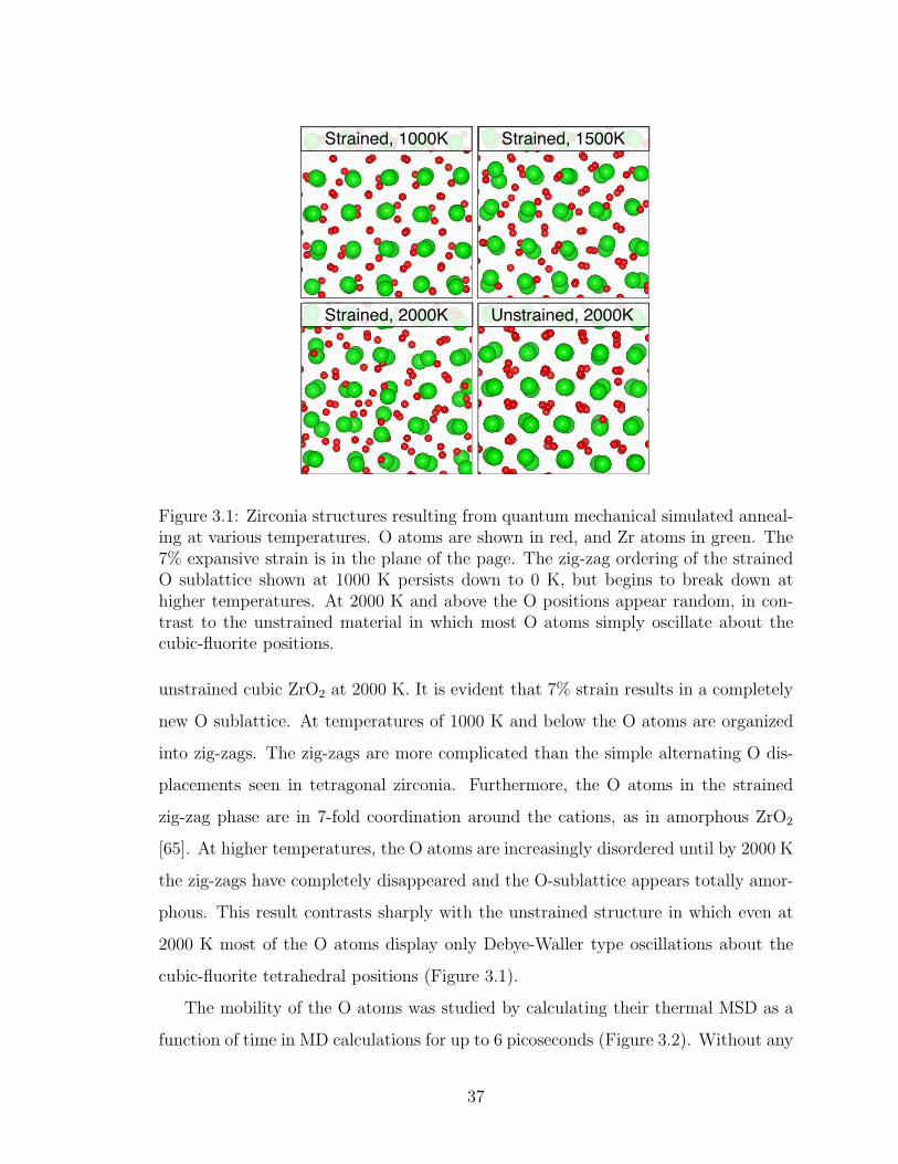
Unstrained, 2000KStrained, 2000K
Strained, 1000K Strained, 1500K
Figure 3.1: Zirconia structures resulting from quantum mechanical simulated anneal-ing at various temperatures. O atoms are shown in red, and Zr atoms in green. The7% expansive strain is in the plane of the page. The zig-zag ordering of the strainedO sublattice shown at 1000 K persists down to 0 K, but begins to break down athigher temperatures. At 2000 K and above the O positions appear random, in con-trast to the unstrained material in which most O atoms simply oscillate about thecubic-fluorite positions.
unstrained cubic ZrO2 at 2000 K. It is evident that 7% strain results in a completely
new O sublattice. At temperatures of 1000 K and below the O atoms are organized
into zig-zags. The zig-zags are more complicated than the simple alternating O dis-
placements seen in tetragonal zirconia. Furthermore, the O atoms in the strained
zig-zag phase are in 7-fold coordination around the cations, as in amorphous ZrO2
[65]. At higher temperatures, the O atoms are increasingly disordered until by 2000 K
the zig-zags have completely disappeared and the O-sublattice appears totally amor-
phous. This result contrasts sharply with the unstrained structure in which even at
2000 K most of the O atoms display only Debye-Waller type oscillations about the
cubic-fluorite tetrahedral positions (Figure 3.1).
The mobility of the O atoms was studied by calculating their thermal MSD as a
function of time in MD calculations for up to 6 picoseconds (Figure 3.2). Without any
37

0
2
4
6
8
10
12
14
1 2 3 4 5 6 7
Oxy
gen
MS
D (
Å2 )
Picoseconds
1000K
unstrained 2500K1500K
2000K
2250K
2500K
-4
-3
-2
-1
0.4 0.7 1
ln(D
/dt)
1000/T (1/K)
Figure 3.2: MSD of O atoms as a function of time during MD simulations at varioustemperatures. (Inset) Arrhenius plot of D from the strained MSDs (same units). Thelinear fit shown in green yields an energy barrier of 0.4± 0.1 eV.
vacancies, no net displacement occurs. Even with one vacancy per supercell at 2000 K,
the superionic unstrained zirconia still produces no MSD on this timescale. Applying
7% strain to the zirconia with a single vacancy, however, I find that significant O
MSD occurs as low as 1000 K. As no motion occurs without vacancies, the mobility
is therefore not mediated by “sublattice melting” but by vacancy hopping.
With vacancies, the strained zirconia O MSD increases with temperature and
correlates with the degree of disorder. At 1000 K and 1500 K, where a degree of zig-
zag ordering remains, plateaus occur in the MSD corresponding to periods of time
without hopping. At 2000 K and above, where the O sublattice appears random, the
MSD increases continuously. The activation barrier extracted from an Arrhenius plot
of the diffusivities (Figure 3.2 inset) is 0.4± 0.1 eV, smaller than the 0.6 eV reported
by [58].
To investigate the role of the interface, I determined the structure down to 360 K
by performing simulated annealing of the STO-YSZ multilayers starting from 1200 K,
which is roughly the substrate temperature used during growth of the multilayers in
the experiment. The result is shown in Figure 3.3. Unlike in the bulk strained zirconia,
the O sublattice near the interface remains highly disordered all the way down to 360
38
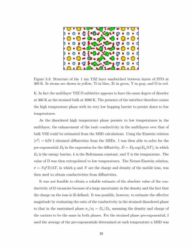
Figure 3.3: Structure of the 1 nm YSZ layer sandwiched between layers of STO at360 K. Sr atoms are shown in yellow, Ti in blue, Zr in green, Y in gray, and O in red.
K. In fact the multilayer YSZ O sublattice appears to have the same degree of disorder
at 360 K as the strained bulk at 2000 K. The presence of the interface therefore causes
the high temperature phase with its very low hopping barrier to persist down to low
temperatures.
As the disordered high temperature phase persists to low temperatures in the
multilayer, the enhancement of the ionic conductivity in the multilayers over that of
bulk YSZ could be estimated from the MSD calculations. Using the Einstein relation
〈r2〉 = 6Dt I obtained diffusivities from the MSDs. I was then able to solve for the
pre-exponential D0 in the expression for the diffusivity, D = D0 exp(Eb/kT ), in which
Eb is the energy barrier, k is the Boltzmann constant, and T is the temperature. The
value of D was then extrapolated to low temperatures. The Nernst-Einstein relation,
σ = Nq2D/kT, in which q and N are the charge and density of the mobile ions, was
then used to obtain conductivities from diffusivities.
It was not feasible to obtain a reliable estimate of the absolute value of the con-
ductivity of O vacancies because of a large uncertainty in the density and the fact that
the charge on the ions is ill-defined. It was possible, however, to estimate the effective
magnitude by evaluating the ratio of the conductivity in the strained disordered phase
to that in the unstrained phase σs/σb = Ds/Db, assuming the density and charge of
the carriers to be the same in both phases. For the strained phase pre-exponential, I
used the average of the pre-exponentials determined at each temperature a MSD was
39

calculated. As previously noted, the unstrained phase was not conductive enough
to show any net motion even at 2000 K. By increasing the temperature to 2500 K,
however, I was able to get a single MSD slope for the unstrained phase. As an energy
barrier cannot be obtained from a single temperature, I used the 1.1 eV experimental
energy barrier for the unstrained bulk material [58] in the expression for Db. Using
this method, I estimated the ionic conductivity of the strained disordered phase to
be 4×10⁶ times higher than that of unstrained bulk YSZ at 500 K, close to the eight
orders of magnitude reported experimentally.
It is evident that the disorder induced by the strain and the presence of the
interface are responsible for the majority of the observed colossal enhancement in
ionic conductivity. In halide based multilayers such as BaF2/CaF2, space charge
effects enhance ionic conduction up to about two orders of magnitude for thin layers
[50]. Our estimate for the conductivity enhancement in the thin YSZ multilayers does
not include space charge effects, so it may well be that space charge effects provides
the last 1-2 orders of magnitude enhancement.
The results of the simulations also allowed us to gain further insights into the cause
of the extreme O sublattice disorder in the YSZ layer of the multilayer structure. The
O sublattice of bulk zirconia under 7% strain exhibits essentially the same zig-zag
ordering as shown at 1000 K in Figure 3.1 all the way down to 0 K. It is this zig-zag-
ordered sublattice that is juxtaposed with the STO O sublattice. The zig-zag ordered
YSZ O atoms occupy sites that are close to tetrahedral positions. On the other hand,
O atoms in STO occupy octahedral positions. Evidently, the incompatibility of the
STO and YSZ O sublattices is causing the observed O disorder. Figure 3.3 shows
that at 360 K there are relatively small O-atom displacements on the STO side of the
interface. In contrast, because the YSZ is strained by 7%, the O sublattice is more
flexible and succumbs to the perturbation, exhibiting extreme disorder. The stable
STO structure controls the positions of the O atoms in the YSZ interfacial plane,
forcing them all to occupy octahedral positions. This constraint then disturbs the O
atoms in the underlying layers of YSZ, with no Ti neighbors, that are free to disorder.
I probed the above issue further by examining the energetics of O vacancies at the
40
YSZ interfacial plane. When one of the octahedral O atoms in the YSZ interfacial
plane is removed and the structure relaxed, an O atom from further into the YSZ
immediately moves to fill the octahedral vacancy. This preference for full occupation
of the octahedral O positions at the interfacial plane is consistent with electron energy-
loss spectra reported in [58] which shows no difference between the Ti oxidation state
at the interface and deep within the STO. As long as there are O atoms occupying all
the octahedral positions in the interfacial plane, the effect of the STO seems to only
be felt through the displacement of neighboring O atoms. When vacancies are placed
in positions away from the interfacial plane the vacancies do not relax to another
layer. These results indicate that vacancy hopping, and therefore ionic conduction
occurs preferentially in a region below the interfacial plane, where the O atoms are
perturbed but unconstrained by the STO.
It is natural to infer that the extreme disorder seen at 360 K in the thin 1 nm
YSZ O sublattice tapers off with distance from the interface in thicker layers of YSZ.
Colossal conductivity, therefore, is likely to occur only in a relatively thin section of
the YSZ layer adjacent to the interface. This thin disordered section would completely
dominate the conductivity, resulting in the lack of variation in the conductance with
YSZ thickness observed experimentally for 1-30 nm YSZ layers [58].
Increasing the YSZ layer thickness to 62 nm causes a three-orders-of-magnitude
drop in the ionic conductivity, which was attributed to relaxation due to exceeding
the critical thickness of the YSZ [58]. Lattice mismatch theory for epitaxial films,
however, suggests that for 7% mismatch strain, the critical thickness ought to be
extremely small [60], not on the scale of tens of nanometers. The present calculations
resolve this quandary. The zig-zag structure resulting from simulated annealing in the
strained bulk represents a new zirconia phase that becomes energetically favorable at
high strains. Varying the in-plane strain of the zig-zag structure results in a parabolic
dependence of the total energies centered around 5% strain. The total energy of the
5% strained zig-zag structure is only about 0.16 eV per unit cell higher than the total
energy of the unstrained cubic fluorite structure. At 7%, the total energy of the zig-
zag structure is 0.49 eV higher, but this is still 2.76 eV lower than the cubic fluorite
41
structure strained to the same dimensions. The phase change, therefore, reduces the
energy penalty imposed by the strain, and allows the YSZ layer to remain coherently
strained up to 30 nm. Once the strain is released the present calculations suggest
that the ionic conductivity would drop significantly, as observed.
After publishing these DFT results [66], I turned to microscopy to support the
findings. STEM and EELS measurements were performed on a Nion UltraSTEM
operated at 100 kV using a cold field emission electron source, a corrector capable of
neutralizing up to fifth order aberrations [18] and an Enfina EEL spectrometer. Some
images were also obtained on a VG Microscopes HB501UX with a third order Nion
aberration corrector (indicated in the figure caption). The YSZ/STO heterostructures
were grown in a high oxygen pressure (3 mbar) pure O RF sputtering system and
prepared in cross section or plan view geometry by conventional thinning, dimpling,
and ion milling. The samples were tilted in the microscope to either the 〈100〉 or 〈110〉
cubic zone axis of STO. The principle component analysis (PCA) method of [67] was
used to eliminate noise in atomic-resolution EELS elemental maps as described in
[68].
EELS O K-edge fine structure simulations were performed using the Z+1 approx-
imation [69, 70] . The calculations were carried out using DFT as implemented in the
VASP code. For faster convergence with respect to the k-point sampling density and
greater accuracy, the linear tetrahedron method with Bloechl corrections was used
for Brillouin zone integrations [62].
Image simulations were carried out using a absorptive multislice STEM code [71]
with absorption due to thermal diffuse scattering included using an Einstein Model
[72]. The inelastic scattering coeffiecients for EELS were calculated using relativisti-
cally corrected Hartree Fock bound states and Hartree Slater continuum states [73].
An aberration free probe with a aperture semiangle of 30 mrad was assumed. Simu-
lations were for a specimen thickness of approximately 110 A with an EELS detector
semiangle of 30 mrad. A Gaussian blur with a full width half maximum of 1 A was
applied to account for the finite source size.
Due to the propensity of YSZ to facet, growing flat coherent YSZ/STO thin
42

(a) (b)
5 nm 10 nm
Figure 3.4: Low magnification ADF images of YSZ/STO thin film multilayers ac-quired on a VG Microscopes HB501UX. (a) Sample showing flat coherent multilayersgrown in 2007. (b) Sample grown under slightly different growth conditions in 2009showing incoherent layers.
film multilayers is quite challenging. Figure 3.4 shows low magnification annular
dark field (ADF) images of two YSZ/STO samples, one grown in 2007 [58] and the
other in 2009. Although both were grown using the same high pressure oxygen RF
sputtering equipment under similar growth conditions, the layers in the 2007 sample
are coherent and flat while those in the 2009 sample are not. Slight differences in the
growth environment caused the YSZ in the 2009 sample to clump, facet, and bend.
Dislocation cores formed at the interfaces, relieving the strain on the YSZ layers.
In an effort to recreate the coherent YSZ/STO multilayers grown in 2007, samples
were grown with thinner nominal YSZ layer thicknesses. These samples often showed
islanding, as shown in the high resolution ADF image shown in Figure 3.5, in which
clumps of YSZ have formed surrounded on all sides by STO. They also possess coher-
ent areas in which the YSZ is strained to match the STO, such as the area pointed
to by the arrow in Figure 3.5(a) below the more obvious incoherent facet of the YSZ
island. A similar island is shown in the high resolution ADF image shown in Figure
3.5(b) and in an ADF image (3.5(c)) recorded simultaneously with a spectrum image
43

(a)
(b) (c) (d)
1 nm
1 nm
Figure 3.5: High resolution ADF images of islands of YSZ in STO are shown in (a)and (b). The arrow in (a) points to a section of coherent YSZ/STO. An elementalmap created from a spectrum image of the the area imaged in (b) is shown alongsidea simultaneously acquired ADF image (c) in (d). Red, green and blue channels of (d)are composed of the integrated intensities of the O K, Zr M2,3 and M4,5, and Ti L2,3
edges respectively, causing STO to appear purple and YSZ yellow.
of the area used to create the elemental map shown in 3.5(d). The elemental map
shows the integrated intensities of the O K, Zr M2,3 and M4,5, and Ti L2,3 edges as the
red, green and blue channels of the image. Integration windows of approximately 50,
180, and 25 eV were used for the O, Zr, and Ti signals respectively. The only other
features that should affect the signal in the large integration window used for Zr are
the Y M4,5 and M2,3 edges, but this was fine as I was interested in distinguishing YSZ
from STO. Red and blue make purple while red and green make yellow, so STO will
appear purple and YSZ yellow. The island is clearly zirconia.
Figure 3.6 shows coherent interfaces looking down the 〈100〉 and 〈110〉 axes of the
STO. As the YSZ must rotate 45◦ to fit the STO cation lattice, these correspond to
the 〈110〉 and 〈100〉 axes of the YSZ respectively. Intensity in ADF imaging varies
44

0 10 20 30 40 50Position (Å)
Inte
nsity
Position (Å)
Inte
nsity
0 10 20 30 40 50 60
(a) (b)
1 nm 1 nm
Figure 3.6: High resolution ADF images of sections of coherent regions of YSZ/STOmultilayers looking down the STO 〈100〉 and YSZ 〈110〉 directions in (a) and theSTO 〈110〉 and YSZ 〈100〉 in (b). ADF intensity is plotted as a function of positionalong the long direction of the red boxes for both images in the insets. The intensityis integrated along the direction of the short side of the red boxes. Blue arrowsindicate the transition from consistently high intensity peaks to alternating brightdark peaks in the linetraces, corresponding to the transition from YSZ to STO. Thecorresponding positions on the images are also marked with arrows.
roughly as the square of the atomic number of elements being imaged. With atomic
numbers 38, 39 and 40, respectively, Sr, Y and Zr are neighbors on the periodic
table and will therefore appear similarly bright compared to Ti with atomic number
22. Against the background of these heavier atoms, the O columns are not readily
discernible. STO therefore appears with equal numbers of bright and dark columns,
while the YSZ columns all appear bright. Linetraces taken in the 〈110〉 directions of
the images in Figure 3.6 show a series of bright columns surrounded by the alternating
bright and dark columns, identifying the YSZ and STO. The areas of the images used
in the linescans are delineated in the figure with red rectangles. Arrows mark the
transitions between the alternating bright and dark columns of STO and the more
consistently bright columns of the YSZ in the linescans and the corresponding points
in the images. The width of the transition from YSZ to STO contrast is roughly one
unit cell, consistent with the expected beam broadening for this sample thickness.
Figure 3.7(a) shows another section of coherent YSZ/STO layers. A spectrum
45
image (SI) was acquired, consisting of EEL spectra taken in a 4×24 pixel grid within
the area shown in the yellow rectangle. An exposure time of 2 seconds was used for
each pixel. During the acquisition of each pixel of the SI, the beam was scanned in a
16×16 pixel subgrid, allowing an ADF image (Figure 3.7(b)) to be recorded at higher
spatial resolution simultaneously with the EELS SI. As sample drift almost always
occurs during the long periods of time needed to record SIs, the higher resolution
simultaneously recorded ADF image is useful in identifying exactly where the spectra
were recorded. From Figure 3.7(b) it is clear that there was some sample drift down
and to the left, but the STO is clearly discerned from the YSZ by its alternating
bright and dark columns. A map of the Ti concentration created from the integrated
background subtracted Ti L-edge is shown in Figure 3.7(c) at the same scale as the
simultaneously recorded ADF. In the STO, bright rows are seen in the Ti map where
darker Ti columns are seen in the ADF image. Near the interface, the Ti intensity
begins to drop. Moving into the layer of more consistently bright atoms, the Ti
intensity continues to decrease, supporting the identification of the layer as YSZ.
EELS fine structure reflects the local bonding environment. Changes in either
bond-lengths or coordination shift or change the intensities of the fine structure
features. In a disordered material, with many slightly different local bonding en-
vironments, the EELS spectrum is the sum of many slightly different fine structure
features. One, therefore, expects the fine structure features of a disordered material
to be blurred out in comparison to an ordered material. I illustrate this effect with
DFT Z+1 O K-edge fine structure simulations for ordered cubic ZrO2 and disordered
O sublattice strained ZrO2. For the ordered structure it is only necessary to calculate
the Z + 1 projected density of states for a single O site, as all the O sites are equiv-
alent. To simulate the fine structure of the disordered material I summed the Z + 1
projected density of states calculated for 6 different O atoms in the high temperature
disordered O sublattice strained bulk structure produced by the MD calculations of
reference [66]. Monkhorst-Pack k-point meshes of up to 18 × 18 × 18 were used for
the small ordered supercell and up to 4× 4× 4 for the much larger disordered O sub-
lattice structure. The resulting spectra were convolved with a 0.5 eV full width half
46

(a) (b) (c)
1 nm
Figure 3.7: (a) High resolution ADF image of a 〈100〉 YSZ layer sandwiched between〈110〉 STO layers. A SI was acquired from the area indicated by the yellow rectanglesuperimposed on (a). An ADF image recorded simultaneously with the SI is shownin (b) at the same scale as the Ti elemental map shown in (c). A drop in the Tiintensity correlates with the more consistently bright columns of the YSZ layer.
maximum Gaussian to facilitate comparison to experiment. The results are shown in
Figure 3.8 normalized to the integrated intensity of the first 50 eV of the edges. The
simulated fine structure features of the ordered structure correspond well to those
seen in normal bulk YSZ. Shifts in the features of the projected density of states for
each of the different Z + 1 sites used in the simulation for the disordered structure
sum up to create a fine structure which appears much like a blurred version of the fine
structure of the ordered structure. Where there are two peaks close together in the
fine structure of the ordered material, there is a single broad peak for the disordered
material.
In Figure 3.9(a) the YSZ O K-edge fine structure obtained from the spectrum
image of the coherent region of the STO/YSZ multilayer shown in Figure 3.7 is com-
pared to that obtained from bulk YSZ. From the simultaneously acquired ADF image
it is easy to pick out which SI pixels are inside the YSZ layer. The spectrum shown
in green in Figure 3.9(a) was created by summing over the 20 SI pixels corresponding
47
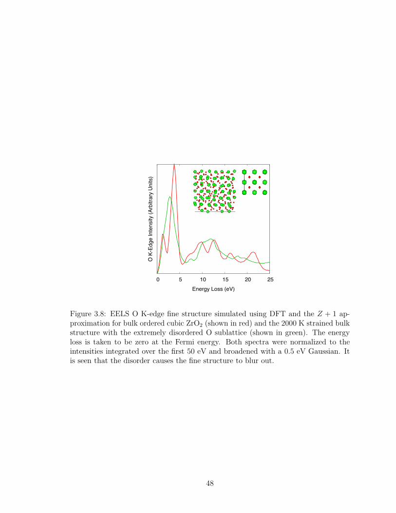
0 5 10 15 20 25
O K
-Edge Inte
nsity (
Arb
itra
ry U
nits)
Energy Loss (eV)
Figure 3.8: EELS O K-edge fine structure simulated using DFT and the Z + 1 ap-proximation for bulk ordered cubic ZrO2 (shown in red) and the 2000 K strained bulkstructure with the extremely disordered O sublattice (shown in green). The energyloss is taken to be zero at the Fermi energy. Both spectra were normalized to theintensities integrated over the first 50 eV and broadened with a 0.5 eV Gaussian. Itis seen that the disorder causes the fine structure to blur out.
48

530 540 550 560
O K
-Ed
ge
In
ten
sity (
Arb
itra
ry U
nits)
Energy Loss (eV)
(a) (b)
Figure 3.9: (a) O K-edge fine structure from the thin YSZ layer shown in Figure3.7 plotted in green and from bulk cubic YSZ in red. The multilayer spectrum wascreated from the same spectrum image used to produce the Ti map in Figure 3.7.Pixels were summed up in the area corresponding to the green box superimposed onthe simultaneous ADF image shown in (b).
to the area within the green box superimposed on the simultaneously acquired ADF
image shown in Figure 3.9(b). With a per pixel exposure time of 2 seconds, this cor-
responds to a 40 second exposure, plenty of time for fine structure to dominate the
noise, yet only broad peaks are seen. Compared to the spectrum from bulk YSZ, the
multilayer spectrum appears blurred out just as predicted by theory for a structure
with O disorder. It is likely there is some contribution to the multilayer spectrum
from STO - the integrated Ti L2,3 signal does not go to zero in the YSZ layer - but
the spectrum does not appear to be a simple linear combination of YSZ and STO
bulk fine structure. STO has a prominent prepeak at very nearly the same energy as
bulk YSZ, yet the multilayer YSZ spectrum has only a weak strength in this region,
supporting the view that the fine structure is blurred out due to O disorder in the
YSZ.
Another way EELS can be used to search for disorder is through atomic-resolution
elemental mapping. Images created from the integrated edge intensities of each pixel
49

(a)
(b)
(c)
(d)
Position (Å)
Intensity
2.8Å
0 10 20 30
Figure 3.10: (a) Model of YSZ/STO multilayer with ordered strained YSZ O sublat-tice viewed such that the STO is seen down the 〈110〉 direction. In this orientationthe pure O columns of STO can be resolved using high spatial resolution elementalmapping. The O columns of the strained ordered YSZ have the same 2.76 A in planeseparation as the pure O columns in STO in the vertical direction of the Figure anda slightly shorter 2.39 A. As such, the YSZ O columns should be resolved in an ele-mental map, if O atoms are ordered. If they are instead disordered as in (b), then onewould expect to see a highly blurred out structure or just a blur. The blurring out isillustrated in (c) with a multislice simulation of the O K-edge elemental map of thestructure shown in (b), viewed in the same orientation. The integrated intensity ofeach column of pixels in the simulated elemental map is shown in (d). The intensityis shown in arbitrary units.
50
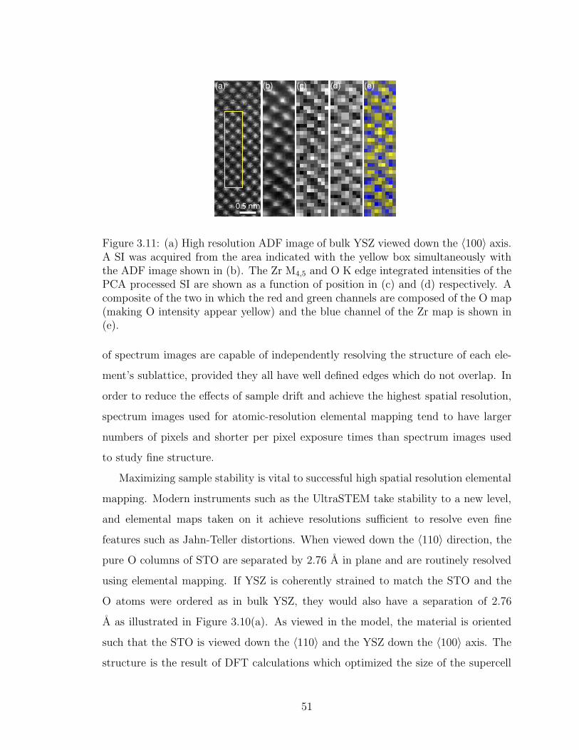
(a) (b) (c) (d) (e)
0.5 nm
Figure 3.11: (a) High resolution ADF image of bulk YSZ viewed down the 〈100〉 axis.A SI was acquired from the area indicated with the yellow box simultaneously withthe ADF image shown in (b). The Zr M4,5 and O K edge integrated intensities of thePCA processed SI are shown as a function of position in (c) and (d) respectively. Acomposite of the two in which the red and green channels are composed of the O map(making O intensity appear yellow) and the blue channel of the Zr map is shown in(e).
of spectrum images are capable of independently resolving the structure of each ele-
ment’s sublattice, provided they all have well defined edges which do not overlap. In
order to reduce the effects of sample drift and achieve the highest spatial resolution,
spectrum images used for atomic-resolution elemental mapping tend to have larger
numbers of pixels and shorter per pixel exposure times than spectrum images used
to study fine structure.
Maximizing sample stability is vital to successful high spatial resolution elemental
mapping. Modern instruments such as the UltraSTEM take stability to a new level,
and elemental maps taken on it achieve resolutions sufficient to resolve even fine
features such as Jahn-Teller distortions. When viewed down the 〈110〉 direction, the
pure O columns of STO are separated by 2.76 A in plane and are routinely resolved
using elemental mapping. If YSZ is coherently strained to match the STO and the
O atoms were ordered as in bulk YSZ, they would also have a separation of 2.76
A as illustrated in Figure 3.10(a). As viewed in the model, the material is oriented
such that the STO is viewed down the 〈110〉 and the YSZ down the 〈100〉 axis. The
structure is the result of DFT calculations which optimized the size of the supercell
51

in the direction perpendicular to the interface. The O spacing in this direction is a
slightly shorter 2.39 A. Both of these lengths are greater than the resolution typically
achieved in EELS maps acquired on the UltraSTEM. Therefore, if the O lattice is
ordered it should be resolved.
Figure 3.10(b) is the result of performing simulated annealing with DFT on the
structure shown in (a). The O sublattice disorders to the point of randomness, as
in the high temperature MD of bulk strained YSZ. A multislice simulation of the O
K-edge elemental map that would result from viewing a sample consisting of the 11
A thick structure shown in Figure 3.10(b) repeated to a thickness of approximately
110 A is shown in Figure 3.10(c). The O columns are clearly resolved in the STO
but appear quite blurred out in the interfacial planes of TiO2 and in the YSZ. The
repetition of the relatively thin supercell used in the DFT calculation to make a thicker
sample imposes order that is not likely to exist in a real sample. In a real sample, O
atoms will be distributed over far more probe positions, causing even greater spatial
blurring than in the simulation. If the YSZ O sublattice is disordered, an O elemental
map should resolve columns in the STO but be only a blur in the YSZ.
To demonstrate that ordered O atoms in YSZ are resolved when viewed down
the 〈100〉 axis, I performed atomic-resolution elemental mapping in bulk YSZ. A
high resolution ADF image of bulk YSZ is shown in Figure 3.11(a). A yellow box
delineates the region nominally used for the spectrum image. An ADF image recorded
simultaneously with the spectrum image is shown in Figure 3.11(b), from which it
is clear what the true positions of the heavy columns were during EELS acquisition.
The SI data were denoised using PCA, and the integrated intensities of the Zr M and
O K edges shown in Figures 3.11(c) and (d) respectively. A composite of the two
maps is shown in Figure 3.11(e) in which the blue channel is composed of the Zr map
and the red and green channels composed of the O map. As such, Zr columns appear
blue and O columns appear yellow. Areas with high intensity in the simultaneous
ADF image correspond to Zr sites, and also appear bright in the Zr elemental map.
The O map also shows a lattice of bright spots. They are between the Zr columns
seen in the ADF as is the correct position of the O atoms in the ordered material.
52

(a) (b) (c) (d) (e) (f) (g) Intensity
1 nm
Figure 3.12: (a) High resolution ADF image of a section of coherent YSZ/STO mul-tilayers viewed down the 〈110〉 STO axis. An ADF image recorded simultaneouslywith a SI taken in the area indicated by the yellow box is shown in (b). IntegratedTi L and O K edge intensity elemental maps extracted from the PCA processed SIare shown in (c) and (d) and as a composite map in (e) in which O intensity is shownin yellow and Ti intensity is shown in blue. An O elemental map extracted from theSI without PCA processing is shown in (f), and the integrated intensity of each rowof pixels in the raw O map is shown in (g). The intensity is given in arbitrary units,with the background subtracted to improve the contrast.
53

Having established that an ordered YSZ O sublattice should be resolved, let us
now turn to elemental maps of the YSZ/STO multilayers. PCA processed Ti and
O elemental maps taken from the boxed area in Figure 3.12(a) are shown in Figures
3.12 (c) and (d) and as a composite in which O is shown in yellow and Ti in blue in
(e). In addition an O map produced from the SI without PCA processing is shown in
(f) and the integrated intensity of each row of pixels in the raw O map is plotted at
the same scale beside it in part (g) of the figure. From the simultaneous ADF image,
(b), it is clear that there was some sample drift over the course of the 6 minutes and
27 seconds it took to acquire the 19×98 pixel SI. The drift is seen to be relatively
uniform and without any large jumps. More importantly the Ti and pure O columns
are clearly resolved in the STO in the elemental maps and in the correct positions
based on the positions of the Sr and Ti columns in the simultaneous ADF image.
In the YSZ region of the O maps, the O lattice blurs out and all but disappears,
consistent with the presence of a disordered YSZ O sublattice.
The ADF images show small variations of intensity between the rows of atoms
inside the YSZ region consistent with the patterning of the surrounding STO, but
with much lower contrast, suggesting there is some STO above or below the YSZ. The
Ti map shows only very weak intensity columns in the YSZ region. Their presence is
significant, however, as the only O columns that appear in the YSZ region in the O
elemental maps are similarly weak, and positioned vertically aligned and horizontally
interspersed with the dim Ti columns. As can be seen from the model in Figure
3.10(a), the spacing between rows of pure O columns in STO is twice that of ordered
YSZ. If the YSZ O atoms were ordered as in the model, one would therefore expect
to see strong peaks at twice the frequency as in STO, not just weak spots in TiO
rows against a relatively uniform background. The lack of such peaks thus strongly
suggests that we are indeed seeing O disorder in the YSZ.
Further support for the presence of a disordered YSZ O sublattice is seen by
comparing the linetraces of the experimental and theoretical O elemental maps. The
average intensity of each row of pixels in the raw O map (Figure 3.12(g)) shows clear
contrast in the STO with peaks corresponding to the TiO2 planes, but very little
54

(a) (b) c
d
e
1 nm1 nm
Figure 3.13: (a) High resolution ADF image of an incoherent YSZ island surroundedby STO. (b) A magnified view of the interface on the left side of the island shown in(a). The green lines are drawn through the centers of the Zr columns, illustrating theexpansive strain that occurs in these regions near the interface.
contrast in the YSZ region. This lack of contrast is similar to that seen in Figure
3.10(d) for the O elemental map simulated for the multilayer structure with extreme
O disorder produced by DFT calculations. I note that the blurring out of the heavy
ions in the YSZ region seen in the ADF images is consistent with the deviations seen
in the Zr positions seen in the simulated multilayer shown in Figure 3.10(b). Although
the Zr atoms are not disordered to the extreme degree of the O atoms, they do not
form perfect columns, which would cause some blurring out of the Zr columns in the
ADF images.
In addition to the coherent STO/YSZ interfaces I also saw evidence for a combi-
nation of strain and O disorder at the interfaces of incoherent YSZ islands and the
surrounding STO. Figure 3.13 shows a high resolution ADF image of a YSZ island.
Strain and disorder are associated with dislocation cores such as those seen in the
magnified view of Figure 3.13. Areas of YSZ expansion and contraction appear along
the interface. The green lines follow the YSZ unit cells from the middle of the island
to the interface where the unit cells are expanded. The lattice spacing around the
55
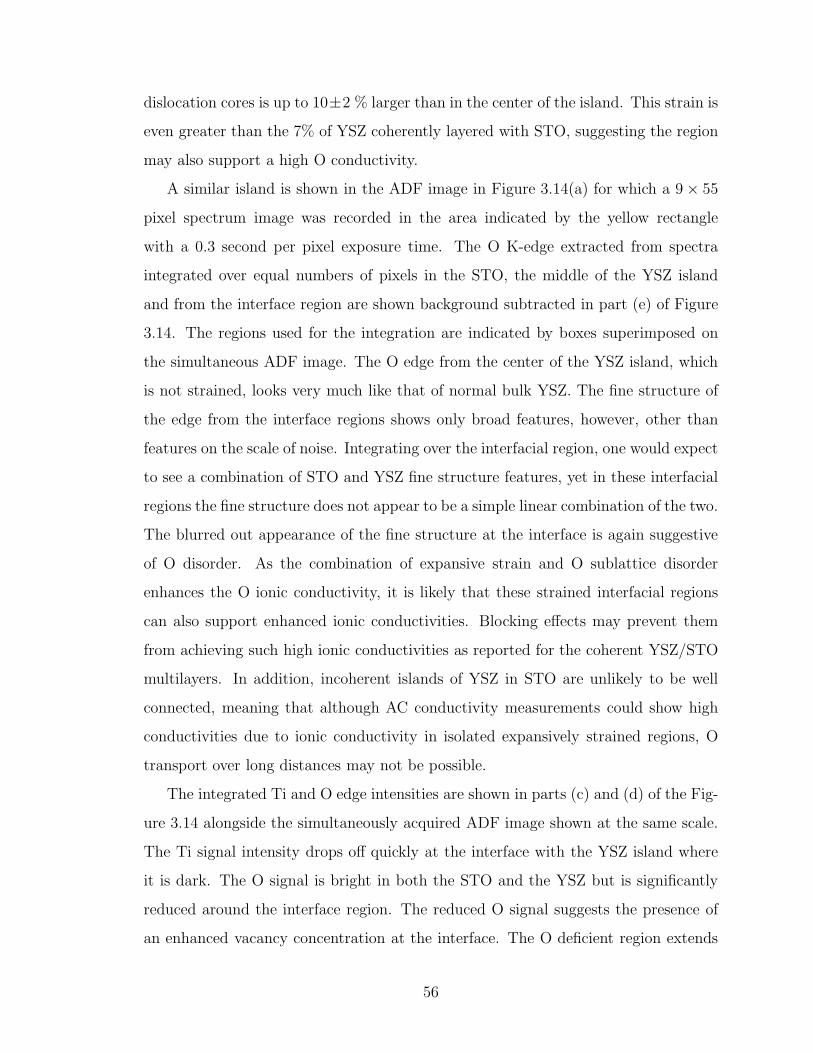
dislocation cores is up to 10±2 % larger than in the center of the island. This strain is
even greater than the 7% of YSZ coherently layered with STO, suggesting the region
may also support a high O conductivity.
A similar island is shown in the ADF image in Figure 3.14(a) for which a 9× 55
pixel spectrum image was recorded in the area indicated by the yellow rectangle
with a 0.3 second per pixel exposure time. The O K-edge extracted from spectra
integrated over equal numbers of pixels in the STO, the middle of the YSZ island
and from the interface region are shown background subtracted in part (e) of Figure
3.14. The regions used for the integration are indicated by boxes superimposed on
the simultaneous ADF image. The O edge from the center of the YSZ island, which
is not strained, looks very much like that of normal bulk YSZ. The fine structure of
the edge from the interface regions shows only broad features, however, other than
features on the scale of noise. Integrating over the interfacial region, one would expect
to see a combination of STO and YSZ fine structure features, yet in these interfacial
regions the fine structure does not appear to be a simple linear combination of the two.
The blurred out appearance of the fine structure at the interface is again suggestive
of O disorder. As the combination of expansive strain and O sublattice disorder
enhances the O ionic conductivity, it is likely that these strained interfacial regions
can also support enhanced ionic conductivities. Blocking effects may prevent them
from achieving such high ionic conductivities as reported for the coherent YSZ/STO
multilayers. In addition, incoherent islands of YSZ in STO are unlikely to be well
connected, meaning that although AC conductivity measurements could show high
conductivities due to ionic conductivity in isolated expansively strained regions, O
transport over long distances may not be possible.
The integrated Ti and O edge intensities are shown in parts (c) and (d) of the Fig-
ure 3.14 alongside the simultaneously acquired ADF image shown at the same scale.
The Ti signal intensity drops off quickly at the interface with the YSZ island where
it is dark. The O signal is bright in both the STO and the YSZ but is significantly
reduced around the interface region. The reduced O signal suggests the presence of
an enhanced vacancy concentration at the interface. The O deficient region extends
56

(a) (b) (c) (d) (e)
530 540 550 560
O K
-Ed
ge
In
ten
sity (
Arb
itra
ry U
nits)
Energy Loss (eV)
Figure 3.14: (a) High resolution ADF image of an incoherent island of YSZ surroundedby STO. (b) ADF image recorded simultaneously with a SI recorded in the areaindicated by the yellow box in (a). Ti and O elemental maps extracted from the SIare shown in (c) and (d) at the same scale as (b). The O K-edge extracted fromthe regions indicated by the corresponding colors in (b) are shown in (e). The greenspectrum shows a significant reduction in the continuum region of the spectrum,indicating the presence of O vacancies.
57
into the STO. O deficiency at dislocation cores in STO and related structures and
its effect on current transport has been reported previously [74, 75]. Vacancies cause
STO to become metallic.
Experiments on samples of STO containing YSZ islands have been reported by
Cavallaro et al. [76], which they believe show the majority of the conduction occurring
in samples they have grown by pulsed laser deposition to be electronic in nature.
They report a one order of magnitude decrease in the conductance of their material
as they decrease the O partial pressure from 1 bar pure oxygen to 3× 10⁻⁴ bar. The
decrease in partial pressure should increase the number of O vacancies in the material.
The decrease in conductance with partial O pressure they measure could therefore
be explained, as they suggest, by the n-type doping of vacancies compensating an
intrinsic p-type doping of the material. P-type doping could, for instance, be caused
by diffusion of Y into the STO.
Clearly the nature of the conductivity of STO/YSZ nanocomposites depends on
the balance of doping by interdiffusion of ions and the concentration of vacancies in
the STO. Note that DFT calculations suggest that it is energetically unfavorable for O
vacancies to leak out of YSZ into the STO when they are grown in coherent multilayers
[66]. Additionally, the conductivity of the coherent STO/YSZ multilayers grown by
Garcia-Barriocanal et al. showed negligible dependence on the partial oxygen pressure
[58]. These facts support ionic conductivity as the dominant form of the conductivity
observed in the coherent YSZ/STO produced by Garcia-Barriocanal et al. If electronic
conduction was dominant, the change in the STO vacancy concentration introduced
by changing the O partial pressure should have significantly altered the conductivity.
58

CHAPTER IV
ATOM-BY-ATOM IDENTIFICATION OF ATOMS IN SINGLE LAYER
BORON NITRIDE WITH ANNULAR DARK-FIELD STEM AND DFT
Light single layer materials such as graphene and boron nitride have low knock-
on damage thresholds. Even at 100 kV holes are drilled in the sample too quickly
for microscopy to be practical. At 60 kV however, these materials are far more
stable, and it is possible to observe them for many minutes without causing damage.
The development of aberration correction has coincided with the recent explosion of
interest in such light atomically thin materials. This is fortunate as prior to aberration
correction the resolution at low-kV was too poor to observe the atomic structures of
graphene and BN. With aberration correction it is now possible to achieve probe
sizes close to 1 A at 60 kV [20]. As there are no interatomic distances not involving
hydrogen less than 1.2 A, a probe close to 1 A should be sufficient for atomic resolution
imaging of single layer materials.
In order to identify which atom is which in monolayer boron nitride (BN), bright-
field phase-contrast imaging has recently been used [77, 78, 79]. However, because
the bright-field signal is very similar for boron and nitrogen, the two types of atoms
are difficult to distinguish. The only study to distinguish B and N sites in a TEM
had to resort to averaging over 20 different B-N pair locations in order to obtain a
sufficient signal-to-noise ratio. The identification of individual atoms was therefore
not direct, and the technique is not able to image a particular configuration in a
changing sample. EELS, also suffers from a need for long acquisition times, and a
lack of spectral features suitable for an identification at high spatial resolution for
about 50% of elements. The ADF STEM image intensity increases with the atomic
number (Z) of the atom as about Z1.7. This dependence makes the ADF signal from
light atoms much weaker than from heavy ones, and the technique has therefore
not been used much in the past for imaging light atoms. My collaborators and I
59

have now shown that aberration correction allows a STEM to be optimized for low-
voltage operation such that the ADF signal is strong enough to image and identify
the chemical type of light atoms neighboring each other on the periodic table [19].
Figure 4.1(a) shows a high-magnification ADF STEM image of monolayer BN
grown by Valeria Nicolosi, recorded at 60 kV on a Nion UltraSTEM by Matthew F.
Chisholm. The probe size was about 1.2 A. The BN monolayer region was surrounded
by thicker regions, one of which is seen on the left side of the image, and vacuum.
Individual boron and nitrogen atoms are clearly distinguished by their intensity. Each
single hexagonal ring of the BN structure, for instance the one marked by the green
circle in the figure, consists of three brighter nitrogen atoms and three darker boron
atoms. The pattern is repeated throughout the image of the monolayer BN. However,
there are several deviations from this pattern, such as the hexagonal ring marked by
the yellow circle, which shows six atoms with intensities intermediate to those of B
and N.
In order to interpret the irregular features correctly, it was necessary to remove
the contribution from the tail of the electron probe to the nearest-neighbour sites.
If this contribution is present, the tails from the heavier N atoms contribute more
strongly to the B sites than the tails from the lighter B atoms contribute to the N
sites, and the intensities at the two sites cannot be compared quantitatively. Ondrej
L. Krivanek and Niklas Dellby deconvolved the image using a procedure that removed
the tail contribution from the nearest-neighbour sites, and also removed (smoothed)
the pixel-to-pixel statistical noise caused by the spreading of the available signal
among the many pixels in a massively oversampled image. The deconvolved version
of Figure 4.1(a) is shown in Figure 4.1(b).
Figure 4.1(c) shows line profiles through the two locations marked in Figure 4.1(b).
Profile X-X’ starts with two atoms of the hexagonal ring marked by the yellow circle
in Figure 4.1(a). The rings atoms are clearly different from the alternating boron and
nitrogen atoms shown in the rest of the profile. Carbon (Z = 6) substituting for the
B (Z = 5) and N (Z = 7) is the likely explanation. Profile Y-Y’ goes through the
regular B-N pairs, with one exception: the first atom in the profile is significantly
60
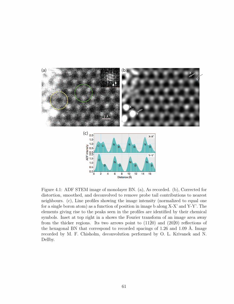
(a) (b)
(c)
Figure 4.1: ADF STEM image of monolayer BN. (a), As recorded. (b), Corrected fordistortion, smoothed, and deconvolved to remove probe tail contributions to nearestneighbours. (c), Line profiles showing the image intensity (normalized to equal onefor a single boron atom) as a function of position in image b along X-X’ and Y-Y’. Theelements giving rise to the peaks seen in the profiles are identified by their chemicalsymbols. Inset at top right in a shows the Fourier transform of an image area awayfrom the thicker regions. Its two arrows point to (1120) and (2020) reflections ofthe hexagonal BN that correspond to recorded spacings of 1.26 and 1.09 A. Imagerecorded by M. F. Chisholm, deconvolution performed by O. L. Krivanek and N.Dellby.
61

(a) (b)
Figure 4.2: Analysis of image intensities. (a), Histogram of the intensities of atomicimage maxima in the monolayer area of Figure 4.1(b). (b), Plot of the averageintensities of the different types of atoms versus their atomic number, Z. The heightsof the rectangles shown for B, C, N and O correspond to the experimental error indetermining the mean of each atomic types intensity distribution.
brighter, and is probably oxygen (Z = 8). Without a quantitative statistical analysis,
however, atomic identifications such as these are rather tentative. The appropriate
way to quantify the image is to compute a histogram showing the distribution of the
atom intensities [80, 81] for all the atoms in a given area, and to use the histogram
to determine the probability that the atomic assignments were made correctly. Such
an analysis seems not to have been done before on images of atoms of similar Z.
Figure 4.2(a) shows a histogram of the peak intensities for all the atoms in the
monolayer sample area shown iny Figure 4.1(b) (that is, excluding atoms in the thicker
region on the left side of the figure) created by Ondrej L. Krivanek and Niklas Dellby.
The intensities were normalized such that the center of the B peak is 1. A theoretical
fit for the distributions of the different species of the atoms, based on the standard
deviations determined experimentally for the B and N atoms, and extrapolated to
the C and O distributions, is overlaid on the figure. The separation of the histogram
peaks is such that every atom in the analyzed area could be assigned to a particular
species with >99% confidence, with one exception: the atom marked by the arrow in
the histogram. This atoms intensity was 3σC from the mean C value and 5.6σN from
the mean N value, and it was therefore likely to be carbon at 94% confidence level.
In the examined part of the image, no N atoms were assigned to B sites or vice versa.
62
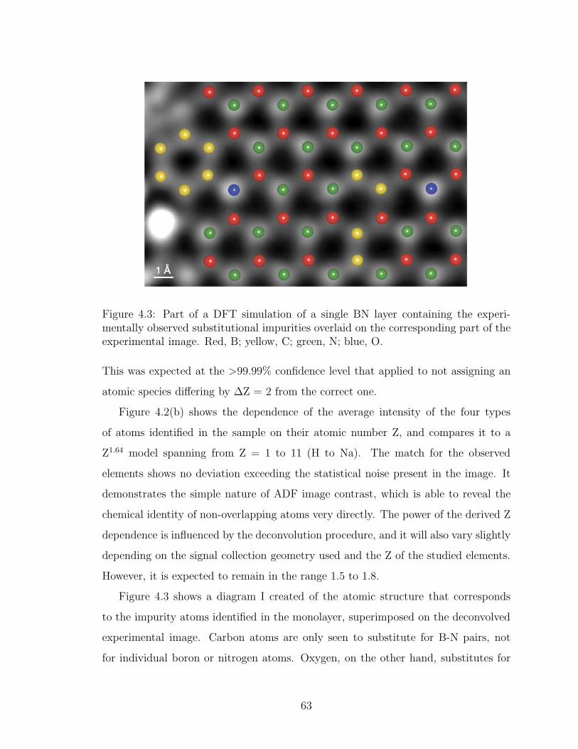
Figure 4.3: Part of a DFT simulation of a single BN layer containing the experi-mentally observed substitutional impurities overlaid on the corresponding part of theexperimental image. Red, B; yellow, C; green, N; blue, O.
This was expected at the >99.99% confidence level that applied to not assigning an
atomic species differing by ∆Z = 2 from the correct one.
Figure 4.2(b) shows the dependence of the average intensity of the four types
of atoms identified in the sample on their atomic number Z, and compares it to a
Z1.64 model spanning from Z = 1 to 11 (H to Na). The match for the observed
elements shows no deviation exceeding the statistical noise present in the image. It
demonstrates the simple nature of ADF image contrast, which is able to reveal the
chemical identity of non-overlapping atoms very directly. The power of the derived Z
dependence is influenced by the deconvolution procedure, and it will also vary slightly
depending on the signal collection geometry used and the Z of the studied elements.
However, it is expected to remain in the range 1.5 to 1.8.
Figure 4.3 shows a diagram I created of the atomic structure that corresponds
to the impurity atoms identified in the monolayer, superimposed on the deconvolved
experimental image. Carbon atoms are only seen to substitute for B-N pairs, not
for individual boron or nitrogen atoms. Oxygen, on the other hand, substitutes for
63

single N atoms. I determined the atomic positions in the diagram by relation with
DFT. The input was a single BN layer containing the substitutional defects identified
by the histogram analysis. The DFT calculations were performed using a plane-
wave basis within the projector-augmented-wave method and generalized-gradient
approximation as implemented in the VASP code. A periodic supercell containing a
single layer of boron nitride consisting of 60 atoms was constructed using the B-N
nearest neighbor separation of 1.45 A. The out of plane dimension of the supercell
was set to 12 A. Carbon atoms were substituted for the B and N atoms of one of the
boron nitride rings, and an O atom substituted for a N atom neighboring the carbon
ring. The structure was then relaxed using an energy cutoff of 400 eV and up to a
3x3x3 Monkhorst-Pack k-point mesh centered at the Γ-point. The resulting supercell
was then doubled in each of the inplane directions and filled with additional single
layer BN and the extra C and O substitutional impurities identified by the histogram
analysis. The resultant 240 atom supercell was relaxed using only the Γ-point in
k-space and an energy cutoff of 400 eV.
Close inspection of Figures 4.1(b) and 4.3 shows that there were significant dis-
tortions in the lattice next to the two oxygen atoms, whose nearest neighbors were
significantly further away than the B-N distance of 1.45 A. One very visible result of
these distortions was that in the hexagonal ring of C atoms, the C nearest neighbor
of the adjacent O atom appears pushed into the carbon ring. This is seen both in
the experimental image, which shows the average distance between the two oxygen
atoms and their nearest neighbors (averaged over the six nearest neighbors of the
two atoms) to be stretched by 0.14 ± 0.08 A relative to the B-N distance of 1.45 A,
and in the DFT-relaxed model, which shows an O-C stretch of 0.09 A. This demon-
strates that even in the presence of statistical noise that shifts the individual atomic
images by small random amounts, ADF imaging is at present able to track atomic
displacements with a precision of about 0.1 A.
In summary, ADF imaging in an aberration-corrected STEM operated at 60 kV
primary voltage has allowed us to determine the positions and the chemical types of
all the atoms in a significant part of an unknown, non-periodic material. Looking
64

towards the future, note that the ADF signal originates from electron scattering by
the atomic nucleus, and that the potentially attainable ADF resolution is therefore
much sharper than the conventional atomic size that is determined by the diameter of
the outermost electron orbitals. As instrumentation advances improve the resolution
of electron microscopes even further in the future, the ADF signal from individual
atoms will be focused into smaller and smaller image areas. This will improve the
signal-to-noise ratios of individual atomic images recorded at a given electron dose,
and the atoms will become easier to identify unambiguously even in complicated
projections.
65

CHAPTER V
HYBRID DENSITY FUNCTIONAL THEORY APPLIED TO LCMO
Transition metal oxides are often considered too complex for DFT in the LDA or
GGA approximations because of the 3d electrons. It is widely believed that a Hubbard
U is needed to account for strong correlations. A phase diagram of LaxCa1−xMnO3
adapted from data reported in [82, 83] is shown in Figure 5.1. It begins with LMO
on the left, which is an anti-ferromagnet (AFM) at low temperatures. Doping LMO
with Ca causes the material to turn into a ferromagnet (FM) for x < 0.5. The doped
LMO remains an insulator until between x = 0.1 to 0.2, after which it becomes a
metal until around x = 0.5, after which LCMO becomes an AFM insulator.
The results of Luo et al. comparing the predictions of GGA and GGA+U at
three values of x are shown in Figure 5.2. The vertical axis displays the difference
in total energy predicted for the AFM and FM magnetic orders in meV. Negative
values indicate the AFM order is more energetically favored whereas positive values
indicate that the FM order is favored. Using both the experimental volumes and the
theoretically predicted volumes for CMO and La0.5Ca0.5MnO3 with ordered dopants
produced superior results to GGA+U. In principle, calculations with dopants should
be performed using large supercells with different dopant arrangements followed by
averaging over such arrangements. Such a series of calculations is not practical. A
method to circumvent the need for such an arduous series of calculations is “generic
doping” in which extra electrons are introduced or removed and compensated for with
a uniform background charge. The validity of generic doping is supported by the fact
that the total energies produced for La0.5Ca0.5MnO3 using it and ordered doping were
very similar. Using ordered doping for x = 0.33 was not possible, and the generic
doping method allowed the GGA to be compared to GGA+U for La0.33Ca0.67MnO3.
Again, GGA outperformed GGA+U. In every case GGA+U decreased the energy
advantage of the experimentally observed AFM phase, and with U = 8 eV for all
points with x ≤ 0.5 the FM structure was considerably more energetically favorable.
66
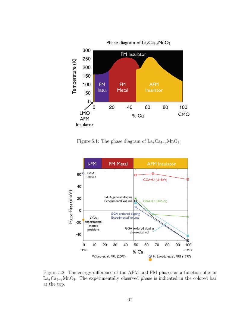
0
50
100
150
200
250
300
0 20 40 60 80 100
Te
mp
era
ture
(K
)
% Ca
Phase diagram of LaxCa1-xMnO3
LMOAFM
Insulator
AFMInsulator
FMMetal
FMInsu.
PM Insulator
CMO
Figure 5.1: The phase diagram of LaxCa1−xMnO3.
-40
-20
0
20
40
60
0 10 20 30 40 50 60 70 80 90 100
AFM InsulatorFM Metali-FM
EA
FM
-EF
M (
meV
)
% CaLMO CMO
GGA+U (U=8eV)
GGA+U (U=5eV)
GGA ordered dopingtheoretical vol
W. Luo et. al., PRL (2007) H. Sawada et. al., PRB (1997)
GGAexperimental
atomic positions
GGARelaxed
GGA generic dopingExperimental Volume
GGA ordered dopingExperimental Volume
Figure 5.2: The energy difference of the AFM and FM phases as a function of x inLaxCa1−xMnO3. The experimentally observed phase is indicated in the colored barat the top.
67

With U = 5 eV, the GGA+U results were better, predicting AFM for CMO and
x = 0.33, but FM for x = 0.5. GGA also produced a FM phase lower in energy than
the AFM phase for x = 0.5, but the difference in energy was smaller.
These results suggest that the U is not helping, but hindering the calculations of
the magnetic ordering for LCMO. On the other hand, GGA+U calculations predict
the correct structure and AFM magnetic ordering for LMO, whereas GGA slightly
underestimates the Jahn-Teller distortions causing it to predict a FM magnetic order-
ing. If however the experimental structure is enforced, GGA does predict the correct
AFM magnetic ordering. The two methods, GGA and GGA+U, also produce incon-
sistent band structure. New exchange-correlation functionals have recently become
available that do very well in correcting the well-known band gap problem of semi-
conductors and insulators. To test if such a hybrid functional might provide more
accurate and consistent results I performed calculations with the HSE06 hybrid den-
sity functional [84] to predict the structure and magnetic order for several members
of the LaxCa1−xMnO3 series.
Hybrid functionals use an admixture of the DFT and Hartree-Fock exchange func-
tionals. The PBE0 hybrid functional [85, 86, 87, 88] is based on the PBE DFT ex-
change correlation functional of Perdue et al. [89], and uses the exchange-correlation
energy
EPBE0xc = aEHF
x + (1− a)EPBEx + EPBE
c ,
where EHFx is Hartree-Fock exchange, EPBE
x is the PBE exchange functional and
EPBEc is the PBE correlation functional. The HSE06 hybrid functional [84] reduces
the computational complexity by using a screened Coulomb potential for the Hartree-
Fock exchange EHFx . The PBE0 functional is used for interactions inside a given
radius, and the PBE GGA functional is used for interactions outside that radius. I
used this functional as implemented in the VASP code. Strict HSE06 uses a value
of 1/4 for a [90], and although other values can be used, I used this value in the
calculations.
In LMO, the hybrid functional slightly overestimates the Jahn-Teller distortions
by a similar amount as GGA underestimates them. HSE06 gives a C/A ratio of 1.14,
68

AB
C
Figure 5.3: The LMO supercell after relaxation with HSE06 (left) with an isolatedoxygen octahedron with bond lengths labeled as used to describe the Jahn-Tellerdistortions (right).
GGA a ratio of 1.07, and the experimentally determined ratio is 1.11. For the C/B
ratio HSE06 gives a value of 1.16, GGA a value of 1.08, and the experimentally deter-
mined value is 1.15. So HSE06 does a slightly better job of predicting the Jahn-Teller
distortions than GGA. Probably because it slightly overestimates the distortions,
HSE06 also predicts the correct magnetic ordering after relaxing the structure, unlike
GGA.
Unlike GGA+U, the hybrid functional also predicts the correct magnetic ordering
for LaxCa1−xMnO3 at x = 0 (CMO), x = 0.33, and x = 0.50 as well. Table 5.1 gives
a comparison of the energy differences EAFM − EFM . These points however are all
AFM insulating phases. Due to the large number of kpoints needed to accurately
simulate metals, it was not possible to test the functional for the metallic points on
the phase diagram. So it is possible that the functional might introduce a systematic
bias in favor of AFM. The computational expense of using the hybrid functional was
also a severe limitation. The calculations of the two end materials, CMO and LMO,
69

were very computationally demanding. I was only able to converge the relaxation
with up to a 4 × 4 × 4 Monkhorst-Pack grid for CMO and only a 2 × 2 × 2 grid for
LMO. The intermediate phases have considerably larger supercells, and I was only
able to converge the relaxation with up to 2 kpoints for these structures. The inability
to use higher kpoint samplings for these intermediate phases makes it hard to draw
any useful conclusions for these phases. With a higher kpoint density, the FM phase
might become the preferred order. The computational cost of such hybrid functionals
would therefore seem to make them at present impractical for many of the systems
of interest today, which tend to require larger supercells.
Table 5.1: Energy difference between the AFM and FM magnetic orders as calculatedby HSE06.
LMO La0.5Ca0.5MnO3 La0.33Ca0.67MnO3 CMOEAFM −EFM (eV) −0.015 −0.18 −0.31 −0.106
70

CHAPTER VI
OPTICAL GAPS OF FREE AND EMBEDDED SI NANOCLUSTERS:
DENSITY FUNCTIONAL THEORY CALCULATIONS
The tunable optical properties of nanoclusters make them attractive candidates
for a diverse variety of applications. Among these are lasers, biomarkers, solar cells,
displays and optoelectronics, for which Si nanoclusters (Si-NCs) are of particular
interest [91, 92, 93, 94, 95, 96]. Simulations show that the optical band gap of perfect
isolated Si-NCs increases roughly as the inverse of their diameter from the bulk Si
gap of 1.1 eV to 5 eV or more [97, 98, 94]. Real Si-NCs are rarely isolated or perfect,
however, and experimental reports of the tunable range of the gap vary significantly.
For Si-NCs greater than 3 nm in diameter, the optical gaps generally increase with
decreasing diameter as predicted for perfect isolated Si-NCs. Below 3 nm however,
the energy gaps open up much more slowly, reaching only 2-3.5 eV [99, 100, 101, 102,
103, 104, 105]. The optical properties of Si-NCs have also been studied over a wider
range of energies [106, 107, 108].
Many studies have been devoted to understanding the optical gaps of small Si-NCs.
The observation that Si-NCs with photoluminescence (PL) peak energies between 2-3
eV all had PL peaks at ∼2 eV after exposure to oxygen [100] led many to believe
that O bonds on the surface of the NCs cause the reduced optical gaps. Subsequent
theoretical studies [100, 94, 109, 110, 111, 112, 113, 114, 115] showed that O atoms
bonded to the surface of ideal Si-NCs indeed introduce localized defect states within
the band gaps, reducing or eliminating the opening of the HOMO-LUMO gaps due
to quantum confinement. Other experimental studies have reported little difference
in the optical gaps with or without O, but the gaps are still considerably smaller
than would be expected for a perfect isolated nanocluster [103, 116]. More recent
theoretical studies have considered nanoclusters that are not isolated, but embedded
in SiO2[117, 118, 119, 120, 110, 121, 95, 122, 123, 124]. These studies revealed that
the HOMO or LUMO charge densities extend into the oxide overlayer, reducing the
71

confinement and therefore the gaps. Additionally, an effort has recently been made to
realistically simulate the deformation of NCs that can occur when they are embedded
in an amorphous matrix [125]. Calculations of the densities of states (DOS) reveal
that deformation alone can cause significant changes to the band gap [122].
In this chapter I compare the effects of deformation, O impurities, and oxide cov-
erage on the optical gaps of small Si-NCs using real-space linear response calculations
within the time-dependent local-density approximation (TDLDA) [126]. The TDLDA
approach extends ground state density-functional theory to better describe excited
states and optical transition probabilities. TDLDA significantly increases the opti-
cal gaps of semiconductor and s- and d-electron metal nanoclusters, bringing them
into much better alignment with experimental values than LDA [109, 127]. So far
TDLDA has been used to study free Si nanoclusters [109, 128]. By systematically
comparing the photoabsorption for undeformed and deformed 0.75 nm clusters as
they are increasingly oxidized I demonstrate that deformation, O impurities and ox-
ide coverage all decrease the size of the optical gaps. Furthermore, by examining the
charge densities of the states that are actually involved in the lowest energy optical
transitions I show that both localized defect states and reduced quantum confinement
due to wavefunction spillage cause reduction of the optical gap. These observations
explain the wide variety of experimental results seen for Si-NCs both in porous Si
and embedded in SiO2.
The deformed Si-NCs embedded in amorphous SiO2 were generated as in [125,
122], starting with a supercell of SiO2 containing 192 atoms in the cubic β-crystobalite
structure, which is the closest to the diamond structure among the SiO2 polymorphs.
The supercell is 14.32 A on each side. The O atoms within a 0.75 nm sphere are
removed, leaving behind an embedded 13 atom Si-NC. The structure is then relaxed
using DFT before the SiO2 is amorphized and the Si-NC deformed. The DFT relax-
ations were performed in the generalized-gradient approximation with a plane-wave
basis and projected-augmented wave potentials as implemented in the VASP code.
The calculations were performed using only the Γ point in k-space with an energy
72
cutoff of 400 eV. The residual forces on the atoms in the relaxed structure were less
than 1 meV/A.
To amorphize SiO2 and deform the embedded Si-NCs my collaborator, George
Hadjisavvas, used the Monte Carlo (MC) algorithm of Wooten et al. [129]. This
method is a well established means of generating continuous random networks from
perfect crystals using bond breaking and switching moves. A Keating-like valence
force model [130, 131] was used to approximate the energy of the system. After
each attempted move the structure around the bond was relaxed using a steepest-
descent method, minimizing the forces on the atoms. The energy of the relaxed
structure was then compared to the energy before the attempted move, and the move
is accepted or rejected according to the Metropolis criterion. Bond switching moves
were periodically followed by volume relaxation to relieve stresses in the system.
Bond switching was first performed in only the oxide at high temperature (kBT =
3eV) for 40,000 moves, allowing it to liquify. The temperature is subsequently grad-
ually reduced to kBT = 0.1 eV over more than 106 moves, leaving the oxide in a
glassy amorphous state. Additional bond switching was then performed by Hadjisav-
vas allowing moves in the NC as well as the oxide for 3 × 10⁶ moves. This last step
topologically equilibrates the composite system and deforms the Si-NC.
To separate the effects of the oxide matrix and the O bonded to the surface
of the NC on the photoabsorption, Hadjisavvas produced structures in which we
progressively removed layers of the SiO2, leaving behind the two O atoms bridge
bonded to the NC which resulted from the deformation process. Hadjisavvas next
produced structures in which we stripped off these remaining O atoms one at a time.
He also placed a single double bonded O atom on the surface of the stripped cluster so
I could check what effect it would have compared to the bridge bonds. All dangling
bonds were passivated with H, and I relaxed the resulting structures using DFT
with VASP. To determine the role of deformation, Hadjisavvas also generated a set
of undeformed 13 atom Si-NCs with similar types and levels of oxygen and oxide
coverage. To generate these structures Hadjisavvas started with a supercell of bulk
crystalline Si and removed Si atoms such that we were left with a Si-NC of the same
73
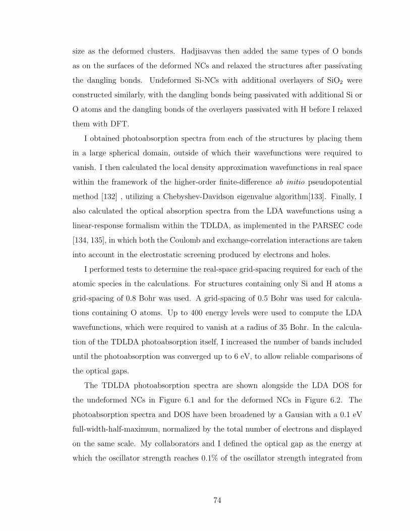
size as the deformed clusters. Hadjisavvas then added the same types of O bonds
as on the surfaces of the deformed NCs and relaxed the structures after passivating
the dangling bonds. Undeformed Si-NCs with additional overlayers of SiO2 were
constructed similarly, with the dangling bonds being passivated with additional Si or
O atoms and the dangling bonds of the overlayers passivated with H before I relaxed
them with DFT.
I obtained photoabsorption spectra from each of the structures by placing them
in a large spherical domain, outside of which their wavefunctions were required to
vanish. I then calculated the local density approximation wavefunctions in real space
within the framework of the higher-order finite-difference ab initio pseudopotential
method [132] , utilizing a Chebyshev-Davidson eigenvalue algorithm[133]. Finally, I
also calculated the optical absorption spectra from the LDA wavefunctions using a
linear-response formalism within the TDLDA, as implemented in the PARSEC code
[134, 135], in which both the Coulomb and exchange-correlation interactions are taken
into account in the electrostatic screening produced by electrons and holes.
I performed tests to determine the real-space grid-spacing required for each of the
atomic species in the calculations. For structures containing only Si and H atoms a
grid-spacing of 0.8 Bohr was used. A grid-spacing of 0.5 Bohr was used for calcula-
tions containing O atoms. Up to 400 energy levels were used to compute the LDA
wavefunctions, which were required to vanish at a radius of 35 Bohr. In the calcula-
tion of the TDLDA photoabsorption itself, I increased the number of bands included
until the photoabsorption was converged up to 6 eV, to allow reliable comparisons of
the optical gaps.
The TDLDA photoabsorption spectra are shown alongside the LDA DOS for
the undeformed NCs in Figure 6.1 and for the deformed NCs in Figure 6.2. The
photoabsorption spectra and DOS have been broadened by a Gausian with a 0.1 eV
full-width-half-maximum, normalized by the total number of electrons and displayed
on the same scale. My collaborators and I defined the optical gap as the energy at
which the oscillator strength reaches 0.1% of the oscillator strength integrated from
74

2 3 4 5 6
Energy (eV)
(f)3.76 eV
(e)3.53 eV
(d)3.07 eV
(c)3.84 eV
(b)4.28 eV
(a)4.86 eV
Photoabsorption
-8 -7 -6 -5 -4 -3 -2 -1 0
Energy (eV)
3.67 eV
3.46 eV
2.87 eV
3.72 eV
4.08 eV
4.66 eV
DOS
Figure 6.1: TDLDA photoabsorption and the LDA DOS for the undeformed Si-NCsat various levels of oxidation. (a) has no O, (b) has one O bridge-bond, (c) has two Obridge-bonds, (d) has one O double-bond, (e) has one layer of oxide, and (f) has twolayers of oxide. The corresponding TDLDA optical and LDA HOMO-LUMO gapsare indicated.
2 3 4 5 6
Energy (eV)
(f)2.89 eV
(e)2.91 eV
(d)2.73 eV
(c)2.89 eV
(b)3.37 eV
(a)3.37 eV
Photoabsorption
-8 -7 -6 -5 -4 -3 -2 -1 0
Energy (eV)
2.79 eV
2.78 eV
2.27 eV
2.75 eV
3.16 eV
3.15 eV
DOS
Figure 6.2: TDLDA photoabsorption and the LDA DOS for the deformed Si-NCs atvarious levels of oxidation. (a) has no O, (b) has one O bridge-bond, (c) has two Obridge-bonds, (d) has one O double-bond, (e) has one layer of oxide, and (f) has twolayers of oxide. The corresponding TDLDA optical and LDA HOMO-LUMO gapsare indicated.
75
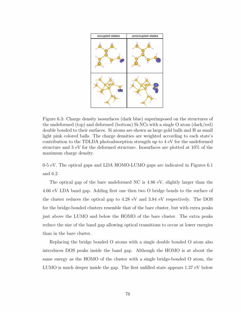
unoccupied statesoccupied states
Figure 6.3: Charge density isosurfaces (dark blue) superimposed on the structures ofthe undeformed (top) and deformed (bottom) Si-NCs with a single O atom (dark/red)double bonded to their surfaces. Si atoms are shown as large gold balls and H as smalllight pink colored balls. The charge densities are weighted according to each state’scontribution to the TDLDA photoabsorption strength up to 4 eV for the undeformedstructure and 3 eV for the deformed structure. Isosurfaces are plotted at 10% of themaximum charge density.
0-5 eV. The optical gaps and LDA HOMO-LUMO gaps are indicated in Figures 6.1
and 6.2.
The optical gap of the bare undeformed NC is 4.86 eV, slightly larger than the
4.66 eV LDA band gap. Adding first one then two O bridge bonds to the surface of
the cluster reduces the optical gap to 4.28 eV and 3.84 eV respectively. The DOS
for the bridge-bonded clusters resemble that of the bare cluster, but with extra peaks
just above the LUMO and below the HOMO of the bare cluster. The extra peaks
reduce the size of the band gap allowing optical transitions to occur at lower energies
than in the bare cluster.
Replacing the bridge bonded O atoms with a single double bonded O atom also
introduces DOS peaks inside the band gap. Although the HOMO is at about the
same energy as the HOMO of the cluster with a single bridge-bonded O atom, the
LUMO is much deeper inside the gap. The first unfilled state appears 1.37 eV below
76
unoccupied statesoccupied states
Figure 6.4: Charge density isosurfaces (dark blue) superimposed on the structures ofthe undeformed (top) and deformed (bottom) Si-NCs with two O (dark/red) atomsbridge bonded to their surfaces. Si atoms are shown as large gold balls and H as smalllight pink colored balls. The charge densities are weighted according to each state’scontribution to the TDLDA photoabsorption strength up to 5 eV for the undeformedstructure and 4 eV for the deformed structure. Isosurfaces are plotted at 10% of themaximum charge density.
the next lowest state in the DOS. The optical gap of the double bonded cluster is
correspondingly smaller, with a size of 3.07 eV.
When a layer of O atoms was added around the cluster with two bridge bonds,
the O atoms passivated the Si atoms and H atoms passivated the O atoms in the
overlayer. Adding the O layer reduced the HOMO-LUMO gap by 0.26 eV. The
optical gap similarly decreased by 0.21 eV. Adding a layer of Si atoms over the O
layer, making a layer of SiO2, increased the HOMO-LUMO gap to 3.67 eV, only 0.05
eV lower than the cluster with just two bridge-bonded O atoms. The optical gap
increases up to 3.76 eV, also only slightly lower than for the cluster with only the two
bridge-bonded O atoms.
With the realistically deformed NCs I found that deformation alone greatly re-
duces the optical gap. The bare deformed cluster had a HOMO-LUMO gap of 3.15
eV and an optical gap of 3.37 eV, both 1.49 eV lower than that of the bare unde-
formed cluster. The only undeformed cluster with smaller gaps was the one with an
77

unoccupied statesoccupied states
Figure 6.5: Charge density isosurfaces (dark blue) superimposed on the structuresof the undeformed (top) and deformed (bottom) Si-NCs with two O atoms bridgebonded to their surfaces and covered in a full layer of SiO2. Si atoms are shown aslarge gold balls, O as smaller red balls and H as small light pink colored balls. Thecharge densities are weighted according to each state’s contribution to the TDLDAphotoabsorption strength up to 4 eV for the undeformed structure and 3 eV for thedeformed structure. Isosurfaces are plotted at 10% of the maximum charge density.
O double bond, the rest all had larger optical and HOMO-LUMO gaps. Adding a
single O bridge-bond made no significant difference to the gaps, as might be expected
from the fact that the deformation reduced the gap more than the double-bond on
the undeformed cluster. The DOS of the deformed cluster with and without a sin-
gle bridge-bond look fairly similar, but the bridge bond added a second peak below
the energy of the HOMO. Correspondingly, a peak appears in the photoabsorption
around 3.8 eV which is not there without the bridge-bond.
The addition of a second bridge-bond moved the HOMO peak slightly down in
energy, but also introduced a peak in the unoccupied DOS significantly lower in
energy than the LUMO of the bare cluster. The optical gap was correspondingly
reduced by 0.48 eV to 2.89 eV. Replacing the bridge bonds with a single double bond
produced similar HOMO and HOMO-1 peaks, but moved the LUMO DOS peak even
lower in energy, resulting in a 2.73 eV optical gap. Note that the TDLDA spectrum
presents an optical excitation at ∼2.3 eV with a nonzero oscillator strength, however
78

its magnitude is small compared to the other optical transitions shown in Figure
6.2(d). As its optical strength is nonzero it is not a forbidden transition. Finally, as
with the undeformed cluster, covering the deformed cluster with two bridge bonds
with SiO2 matrix does not significantly alter the optical gap, suggesting that those O
atoms bonded to the surface of NCs have the most influence on the size of the band
gap.
In order to further investigate the nature of the states that reduce the size of
the optical gaps, I plotted isosurfaces of the charge densities of the states which
are actually participating in the lowest energy TDLDA photoabsorption transitions.
From Figure 6.3 it can be seen that the states introduced into the HOMO-LUMO
gap of the bare clusters by single O atom double-bonds are concentrated around the
O atom. Reducing the isosurface level however, one can see that these states also
extend to other parts of the nanocluster, which explains why the deformation of the
nanocluster would affect the energies of these defect states. The bridge bonds shown
in Figure 6.4 also introduce optical gap-reducing states which are concentrated around
the O atoms. The charge density of these gap-reducing states is less localized than
those introduced by the double bonds, and this may be the reason the optical gaps of
the NCs with bridge bonds are more sensitive to deformation than those with double
bonded O atoms. Finally, one can see from Figure 6.5 that adding a layer of SiO2
over the NCs with bridge bonded O atoms makes only minor differences to the spatial
localization of the states which limit the size of the optical gaps. The charge density
leaks out into the oxide somewhat, explaining the slightly lower optical gaps, but is
mostly concentrated in the same areas of the NCs as without the oxide.
The present results are in agreement with previous theoretical work showing that
the optical gaps of small Si-NCs are reduced by the presence of O bonded to their
surfaces [100, 94, 109, 110, 111, 112, 113, 114]. Previous theoretical studies of em-
bedded Si-NCs agree that the matrix reduces the HOMO-LUMO gaps, but a number
of different conclusions are reached. Some conclude that the gap shrinkage is mainly
due to reduced quantum confinement due to the wavefunctions leaking out into the
matrix [117, 118, 119, 121, 95]. Others show that similar gaps are produced before
79

and after most of the embedding SiO2 have been removed, leaving behind only O
atoms bonded to the surface of the NCs, indicating the importance of O bonds on
the surface of the Si-NCs [124, 123]. Some studies also point out that the interface
between Si-NC and bulk SiO2 matrix is not likely to be abrupt, and that strain and
deformation can reduce the gaps [120, 110, 124, 123, 122]. The present results, the
first produced with TDLDA for embedded clusters, show that deformation and lo-
calized O impurity states have the greatest impact on the size of the optical gaps
of embedded Si-NCs, with reduced confinement due to wavefunction spillage causing
only relatively minor additional closing. Additionally, although deformation and O
bonds on the surfaces of the NCs independently affect the optical gaps, the smallest
gaps are caused by a combination of the two.
From the present calculations it is seen that O bonds and deformation can in-
dependently reduce the sizes of the optical gaps of Si-NCs. Additionally, different
types of O bonds introduce defect states at different energies and result in different
optical gaps. It is clear, however, that when both O and deformation are present, it is
not a simple question as to which independently produces the smaller HOMO-LUMO
gap. O bonded to the surface of the NCs introduces defect states at different energies
depending on whether the NC is deformed or not. The optical gaps of the deformed
clusters are smaller than those of the undeformed clusters by 0.34 eV with a double
bonded O atom and by 0.95 eV with two bridge bonded O atoms. In general, it seems
that the smallest optical gaps are produced with a combination of deformation and
O atoms bonded to the surface of the NCs. In particular, the lowest energy optical
gap of 2.73 eV is produced by the combination of deformation and an O double bond.
Experimental samples of embedded Si-NCs generally contain NCs with a range of
both deformation and O bonds. Macroscale properties such as absorption and pho-
toluminescence depend on the average characteristics. Generally, the largest, most
deformed and oxygenated clusters will limit the optical gap, with the statistical dis-
tribution of the size, deformation and oxidation determining the shape and width of
the optical spectral features. An ideal sample would have a distribution of NCs with
size, deformation and oxidation that was tailored to a particular application. For
80

instance, a narrow photoluminescence peak could be achieved at a high energy by us-
ing free ultrasmall NCs with the same size, negligible deformation, and no O bonded
to their surface. A broad peak could be achieved using NCs of various sizes levels
of deformation and O bonding. Achieving the former presents a difficult challenge,
whereas the latter is what is generally produced.
81
CHAPTER VII
WHITE LIGHT EMISSION FROM ULTRASMALL CDSE
NANOCRYSTALS
Nanotechnology depends on the fact that, as structures are made smaller, they
acquire unique properties. For semiconductor nanocrystals, one consequence of small-
ness is quantum confinement, which widens their energy gaps [136]. The threshold
for absorption and the peak energy of their emission can be finely tuned through their
size. Such control makes quantum dots very useful for lighting applications and as
an alternative to fluorescent dyes in biological imaging [137, 138, 139, 140, 141, 142].
The quest to fully exploit quantum confinement brought with it a push to syn-
thesize progressively smaller and monodisperse nanocrystals. As synthesis methods
improved and reduced the size of nanoparticles into the sub-2-nm range, new prop-
erties emerged. In particular, nanocrystals that exhibit blue-shifted monochromatic
light emission at larger sizes begin to show broad spectra when made ultrasmall
[143, 144, 145, 146, 147, 148]. White light emission from ultrasmall CdSe nanocrys-
tals [149, 150, 151, 152] is a particularly interesting case of such broad emission
because of its potential for solid-state lighting.
It is also particularly intriguing as individual CdSe nanocrystals emit white light
[153], ruling out its explanation as a superposition of narrow emission lines from
nanoparticles of different sizes. On the other hand, it has been suggested that white
light emission involves surface or defect states in the gap [149], but again, defect
and surface states cannot explain the sudden appearance of a continuous spectrum
of transition energies spanning the visual range when the diameter is reduced below
2 nm.
I used a combination of aberration-corrected transmission electron microscopy
and finite-temperature density functional simulations to elucidate the mechanism of
white light emission. A Nion UltraSTEM [18] equipped with a corrector capable of
neutralizing up to fifth-order aberrations was used to obtain the Z-contrast images
82

at 60 kV and 100 kV. A VG Microscopes HB603 with a third-order Nion aberration
corrector was used to acquire Z-contrast images at 300 kV. Both microscopes use a
cold field emission source. Electron energy loss spectroscopy (EELS) was performed
on the UltraSTEM using a Gatan Enfina EEL spectrometer.
The DFT simulations were performed using the generalized-gradient approxima-
tion and the projector-augmented-wave method with a plane-wave basis as imple-
mented in the VASP code. The Cd27Se27 cluster was created by building a large
supercell of bulk CdSe and removing the excess atoms. At least 2 nm of vacuum
separate the atoms of adjacent supercells in the periodic supercell approach. All
calculations were performed at the Γ point in k-space using the pseudopotentials,
constructed for use with the Perdew-Burke-Ernzerhof exchange functional, supplied
with VASP. An energy cutoff of 274.3 eV was used for bare CdSe. The atoms were
allowed to move according to the forces without being constrained to retain any
structural symmetries. Relaxation was performed using VASPs conjugate gradient
method. In the finite-temperature quantum molecular dynamics simulations, atomic
motion time-steps were chosen such that no atom could travel further than 0.1 per
time-step. For bare CdSe we used 8 fs timesteps. For the calculations with ligands
we introduced lighter elements, including H, and thus reduced the timestep to 1 fs.
Because the ligands contain O we also used a higher energy cutoff of 400 eV in the
calculations with ligands.
Optical emission data (collected by James R. McBride) and my Z-contrast scan-
ning transmission electron microscopy (STEM) images from samples of various sizes
of CdSe nanocrystals synthesized by McBride are shown in Figure 7.1. The figure doc-
uments the size and structure dependence of the optical properties. Monochromatic
emission from red to green is seen to correlate with increasingly smaller diameters of
wurtzite nanocrystal (Figure 7.1, (a) to (f)). Around each wurtzite core a fluxional
surface layer of approximately a nanometer in thickness exists, appearing as a blurry
layer in the STEM images (Figure 7.1, (a), (c) and (d)) because of the rapid rate at
which the surface structure changes.
83

The images shown in Figure 7.1(a) to (c) are the result of summing several se-
quential frames from movies with fast per pixel times (1 to 2 microseconds per pixel).
This method has a couple of advantages over using a single image with a long per
pixel time to reduce noise. The nanoclusters tend to tilt on and off axis slightly under
the beam. Using a fast per pixel time movie allows us to choose sequences where the
particle is precisely on axis, whereas with a long per pixel time image, one can only
hope the particle does not shift off axis during acquisition. The sample also tends to
drift during image acquisition, which deforms images performed with a long per pixel
time. Using a drift correction script I was able to align the frames in such movies.
I have used such a script to remove most of drift effects from the images shown in
Figure 7.1 (a) to (c). From these movies, the motion of the surface atoms is obvious.
Moving into the ultrasmall regime produces the broad white-light emission spec-
trum shown in Figure 7.1(g). The STEM observations confirm that the size distribu-
tion of the particles is far too narrow to produce such a spectrum through quantum
confinement alone. Based on their sub-2-nm size, one would expect quantum confine-
ment to produce only colors in the blue to ultra-violet range. The obvious difference
from the larger monochromatic nanocrystals is the absence of the wurtzite crystal
core. Successive frames (Figure 7.1, (g) to (h)) from a Z-contrast STEM movie of a
typical white-light-emitting nanoparticle show it wriggling continuously. It was ac-
quired with a 2 microsecond per pixel time and with a beam accelerating voltage of
60 kV, chosen to minimize knock-on damage. 60 kV is below the calculated knock-on
damage threshold for even light materials such as boron nitride and carbon [154].
Despite operating in this gentle-STEM regime [20], every frame shows a significantly
different structure. A fast per pixel scan time was required to resolve any individual
atoms. Using a longer per pixel time resulted in less noisy images, but the atoms then
move too quickly to be resolved. Using higher accelerating voltages of 100 kV or 300
kV increases the resolution of the STEM images but does not change the qualitative
behavior of the ultrasmall CdSe under the beam. Every frame shows a significantly
different structure at every accelerating voltage. Applying the averaging procedure
84
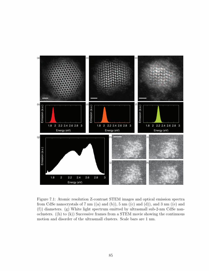
1.8 2 2.2 2.4 2.6 2.8 3
Em
issio
n (
a.u
.)
Energy (eV)
1.8 2 2.2 2.4 2.6 2.8 3
Em
issio
n (
a.u
.)
Energy (eV)
1.8 2 2.2 2.4 2.6 2.8 3
Em
issio
n (
a.u
.)
Energy (eV)
1.8 2 2.2 2.4 2.6 2.8 3
Em
issio
n (
a.u
.)
Energy (eV)
(a)
(b)
(g) (h) (i)
(j) (k)
(e)
(f)
(c)
(d)
Figure 7.1: Atomic resolution Z-contrast STEM images and optical emission spectrafrom CdSe nanocrystals of 7 nm ((a) and (b)), 5 nm ((c) and (d)), and 3 nm ((e) and(f)) diameters. (g) White light spectrum emitted by ultrasmall sub-2-nm CdSe nan-oclusters. ((h) to (k)) Successive frames from a STEM movie showing the continuousmotion and disorder of the ultrasmall clusters. Scale bars are 1 nm.
85

used to produce the images of the larger monochromatic emitting clusters to the ul-
trasmall clusters results in a complete blur. The ultrasmall particles therefore cannot
be regarded as crystalline, and hence I will refer to the white-light emitting struc-
tures as nanoclusters. The disordered fluxional surface layer seen around the larger
nanocrystals appears to have consumed the whole crystal.
EELS was performed to check if the disordered material is the result of oxidation.
The ligands used to synthesize the nanoclusters contain oxygen, so the presence of
some oxygen is not unexpected. The oxygen signal I observed however was too low
to be consistent with the formation of a disordered oxide shell around the CdSe
nanocrystals.
The energy transfer from the fast electron beam is quite sufficient to be the cause
of the continuous fluxional motion. The electron beam is known to impart heat to
crystalline samples via inelastic scattering. The National Institute of Standards and
Technology’s ESTAR program [155] calculates electron stopping powers for electrons
from the theory of Bethe [156, 157], with a density-effect correction evaluated ac-
cording to Sternheimer [158, 159]. For 100 kV electrons ESTAR calculates the linear
collision stopping power to be 1.38 eV/nm for CdSe (with a density of 5.816 g/cm3).
The 100 kV electron beam therefore imparts about 2.8 eV per electron into a 2 nm
CdSe nanocluster.
The white light spectrum spans from 1.7 to 3 eV, and is produced by exciting
the nanoclusters with ultraviolet light. An electron excited by the absorption of a
3-eV ultraviolet photon must therefore loose up to 1.3 eV of energy to vibrations
before emission in the visible spectrum can occur. For a 75-atom cluster, such an
energy amounts to 17 meV per atom added to the existing thermal energy of the
cluster at room temperature. For comparison, at the melting temperature of bulk Si,
individual atoms possess a kinetic energy of 22 meV [160]. Furthermore, the melting
point of nanoclusters decreases rapidly as their size decreases [161, 162, 163, 164, 165,
166]. Clearly something other than simple quantum confinement is causing the white
emission. The only common property of the white light emitting nanoclusters seen by
STEM is their dynamic amorphous structure. I therefore turned to DFT calculations
86

to test if such fluxionality could result from photoexcitation and cause the white light
emission.
Carving out an ultrasmall Cd27Se27 nanocrystal from bulk wurtzite CdSe and
relaxing it gives some hints as to the sensitivity of the electronic structure. Before
relaxation, the nanocluster has no energy gap, but after relaxation it adopts a less
crystalline structure, and a gap opens up. This result is consistent with previous
theoretical work on magic-sized Cd33Se33 [167]. Heating the relaxed cluster up to
room temperature (300 K) using quantum mechanical molecular dynamics, the cluster
disorders further. The atoms move continuously, but after some time the motions look
less wild. Relaxing the structure after the atomic motions have calmed down results
in a structure lower in energy than the cluster relaxed from wurtzite. Therefore, I
concluded that the ultrasmall nanoclusters are intrinsically disordered.
To estimate the effective temperature of a nanocluster that has absorbed an ultra-
violet photon I use simple equipartition, i.e., at temperature T the energy per atom
is (3/2)kT. An electron excited by a 3 eV ultraviolet photon must transfer up to 1.3
eV to vibrations in order for emission to occur in the range of white light emission,
1.7 to 3 eV. For the 54-atom cluster used in the simulations, such energy corresponds
to 24 meV per atom, or an effective temperature of 186 K. When added to room
temperature (300 K), this gives an effective temperature of around 500 K. To account
for the additional vibrational energy imparted after the absorption of an ultraviolet
photon, I therefore performed MD at 500 K . The extra energy makes the motion of
the atoms more rapid and violent. Snapshots from the simulation are shown in Figure
7.2 (a) to (d). The atoms appear to move around as they do in the microscope.
The densities of states (DOS) calculated at 40 fs intervals during part of the 500
K MD simulation are shown in Figure 7.2(e). From this figure it is immediately
clear that the continuous structural fluctuations result in correspondingly fluctuating
energy gaps. The DOS have been colored according to the energy of their lowest
unoccupied state. In determining the color, 1.2 eV was added to the calculated Kohn-
Sham energy gaps, which are well known to be too small compared with measured
values. The value 1.2 eV was chosen so that the first peak in the unoccupied DOS
87

-2 -1 0 1 2 3
1.2 2.2 3.2 4.2
De
nsity o
f S
tate
s (
a.u
.)
Tim
e
Energy (eV)
Shifted Energy (eV)
Tim
e (fs
)
0
40
80
120
160
200
240
280
320
360
400
440
1.8 2 2.2 2.4 2.6 2.8 3 3.2
Sim
ula
ted
Em
issio
n (
a.u
.)
Energy (eV)
1.8 2 2.2 2.4 2.6 2.8 3 3.2
Sim
ula
ted
Em
issio
n (
a.u
.)
Energy (eV)
1.8 2 2.2 2.4 2.6 2.8 3 3.2
Sim
ula
ted
Em
issio
n (
a.u
.)
Energy (eV)
(e) (f)
(f) (g) (h) (i)
Figure 7.2: Density functional simulations of ultrasmall CdSe. ((a) to (d)) Snapshotsfrom a 500 K quantum MD simulation of a Cd27Se27. (e) DOS calculated at 40 fsintervals during the 500 K simulation. The zero of the bottom energy axis has beenset to the DFT Fermi level. The top axis has been shifted 1.2 eV to account for thewell known underestimation of the band gap by DFT. Each DOS has been coloredaccording to the energy of the lowest unoccupied state on this recalibrated axis. (f)An emission spectrum simulated from 20 DOS calculated at intervals of 40 fs.
88

of the relaxed steady-state structures matches the energy at which absorption begins
experimentally. The colors span the range from red to blue. .
The first unoccupied peak in each DOS is separated from the continuous band of
unoccupied states that appear at higher energies. In some cases an additional isolated
peak appears between the first peak and the continuous band of unoccupied states.
If one considers that emission may occur from all of these, the range of potential
emission energies expands. One can get an idea of the spectrum that can be emitted
by simply averaging over emission from the bottom of all the bands at 500 K. Figure
7.2(f) is the result of adding Gaussian peaks at each of these emission energies for
20 sets of DOS calculated at 40 fs intervals during the 500 K MD simulation, the
first 12 of which are those shown in Figure 7.2(e). The energy axis includes the
1.2 eV rigid shift to the conduction band to facilitate comparison to experiment.
The plot simulates the time-averaged emission of an excited ultrasmall nanocluster.
The simulated spectrum matches the width and general shape of the experimental
emission spectra.
I emphasize that the continuous emission spectrum arises from a continuously
varying energy gap caused by the fluxionality. The bonds in the cluster are constantly
and smoothly switching [168]. The evolving electronic states originate from different
regions of the nanocluster, but the regions cannot be categorized as surface, bulk
or trap states. As seen in other semiconductor nanoparticles [94, 169] the charge
density of the states near the band gap are distributed through much of the simulated
ultrasmall CdSe cluster, and therefore cannot be attributed to either surface or bulk
states of the nanocluster. Charge density isosurfaces of the three highest occupied
and three lowest unoccupied states for one of the Cd27Se27 structures produced during
the 500 K molecular dynamics simulation are shown in Figure 7.3. Isosurfaces are
plotted at 1% of the maximum charge density for each band.
The perceived color of the time-averaged emission depends on the shape of the
emission spectrum, not just the range of emission energies. Experimentally, it is ev-
ident that the precise shape of the emission spectrum of ultrasmall CdSe depends
on the mixture of ligands used in their synthesis [152]. All ultrasmall CdSe clusters,
89

(a) (b) (c)
(f)(e)(d)
Figure 7.3: Charge density isosurfaces of the three highest occupied states ((a) to(c)) and three lowest unoccupied states ((d) to (f)) plotted for one of the Cd27Se27structures produced during the 500 K molecular dynamics simulation.
90

however, emit broadly. Furthermore, simulations with partial ligand coverage pro-
duced levels of fluxionality similar to the bare clusters. Extended quantum molecular
dynamics simulations of clusters covered by ligands are not practical, however I did
perform some simulations with partial ligand coverage. I approximated the phos-
phonic acids used in the synthesis of the ultrasmall white light emitting CdSe by
abbreviating the alkane chain to a single methyl group. The abbreviation has been
shown [170] to accurately reproduce the band gap, band edge states, and binding
energies of the full chain molecule on CdSe nanoclusters. First a single ligand was
placed on a prerelaxed Cd27Se27 cluster. The optimal position for the ligand was
found to be one in which it bonds to a Cd atom through the double bonded O atom,
as has been reported before for other sizes of CdSe nanoclusters [170]. I then added
six additional ligands in similar configurations distributed around the cluster, relaxed
the structure, and performed MD. I observed the same kind of fluxionality at 500 K
as I saw with the bare cluster, suggesting that the structural instability is intrinsic
to ultrasmall nanoclusters. The instability is present because of the absence of a
crystalline core and because the ligands do not form a continuously bonded outer
shell. The mixture may tint the broad spectrum toward one color or another, but the
origin of the broad visual spectrum is the fluxionality. The precise balance of colors
is tuned by the ligands to result in the pure white-light emission spectrum.
In conclusion, the ultrasmall size marks the point at which the majority of atoms
in a nanoparticle are at its surface. STEM observations and DFT simulations show
that such a predominance of surface atoms can destabilize nanocrystals, causing them
to take on a dynamic disordered structure. Furthermore, this fluxionality leads to a
dynamic electronic structure. In ultrasmall CdSe, it leads to continuously changing
energy gaps, resulting in their ability to individually exhibit a white time averaged
emission spectrum. Fluxionality also exists at the surfaces of all the larger nanocrys-
tals we have observed, and consequently, the ramifications exceed white light emission.
This description of a nanocrystal surface is quite different from the concept of a stable
trap state and may be relevant to observations of emission from poorly passivated
nanocrystals as well as nanocrystal blinking [171, 172, 173]. F. A. Cotton [174] first
91
advocated the use of the term fluxionality in connection with organometallic molecules
in 1968. Fluxionality of ultrasmall nanoclusters has been invoked in the past in the
context of catalysis [165, 166] and has been discussed by other authors [164, 175, 176].
The present work establishes that fluxionality is the root of white-light emission by
ultrasmall nanoclusters and that it persists at the surfaces of larger nanocrystals that
emit monochromatic light. When optimizing nanocrystals for any application, such as
solar cells, light emitting diodes, photocatalysis or biological imaging agents, dynamic
fluxionality may be a critical consideration.
92
CHAPTER VIII
SUMMARY
In this thesis I used a combination of STEM and DFT to investigate a number of
topical issues in condensed matter and materials physics. After initial explorations
in magnesium oxide, which introduced me to density functional theory calculations, I
studied STO/YSZ multilayers with first-principles calculations. I demonstrated that
the origin of the observed colossal ionic conduction in the multilayers is a combination
of strain on the YSZ and extreme disordering of its O sublattice, with both phenomena
caused by lattice-constant and structure mismatch between the two materials. I also
showed that the misfit strain is sustained because YSZ exhibits a stable phase with
large strain. I then used a combination of STEM and EELS and theoretical EELS
simulations to confirm the presence of a disordered YSZ O sublattice in coherent
YSZ/SrTiO3 multilayers. O K-edge fine structure simulated for the strained disor-
dered O sublattice phase of YSZ possesses blurred-out features compared to that
of ordered cubic bulk YSZ, and experimental EELS fine structure taken from the
strained YSZ of coherent YSZ/SrTiO3 thin films is similarly blurred out. Elemental
mapping was shown to be capable of resolving ordered YSZ O sublattices. Elemental
mapping of O in the coherent YSZ/STO multilayers was presented in which the O
sublattice is seen to be clearly resolved in the STO but blurred out in the YSZ, indi-
cating it to be disordered. In addition, I presented imaging and EELS results which
show that strained regions exist at the incoherent interfaces of YSZ islands in STO
with blurred out fine structure, suggesting these incoherent regions may also support
high ionic conductivities. The presence of a region of O depleted STO at the inter-
face with incoherent YSZ islands was revealed by EELS elemental mapping, implying
the n-type doping of STO/YSZ nanocomposites with disconnected incoherent YSZ
islands.
I described how it is now possible to use STEM with low accelerating voltages to
identify individual atoms in light single layer materials such as BN. My collaborators
93

grew samples of BN and used a Nion UltraSTEM operated at 60 kV to image it.
After using a probe-tail removing technique, they were able to determine from the
Z-contrast image the chemical identify of every atom in a region of single layer BN,
including C and O dopants. I performed DFT calculations to check the viability of
the structure they believed they had identified. The simulation and the experiment
agreed remarkably well, including small changes in bond lengths due to the presence
of the dopants.
I tested the use of so called hybrid density functionals by applying the HSE06 hy-
brid density functional to LaxCa1−xMnO3. GGA outperforms GGA+U at predicting
the magnetic ordering of LCMO for x = 0 to 0.5. However, because GGA slightly
underestimates the Jahn-Teller distortions of LMO, it does not predict the correct
magnetic ordering for x = 1 whereas GGA+U overestimates the distortions and pre-
dicts the correct magnetic ordering. I found the HSE06 hybrid density functional
also slightly overestimates the Jahn-Teller distortions in LMO and gets the correct
magnetic ordering. Unlike GGA+U, the hybrid functional also predicts the correct
magnetic ordering at all the values of x I simulated, x = 0, 0.33, 0.5 and 1. The
computational cost of using the hybrid functional was however a severe limitation,
and the degree of convergence with respect to the number of kpoints for the x = 0.33
and 0.5 phases was not clear as I was not able to use more than 2 kpoints for these
structures. The computational cost of such hybrid functionals would therefore seem
to make them at present impractical for many of the systems of interest today, which
tend to require larger supercells.
Nanotechnology depends on the fact that as structures are made smaller they
acquire new properties. For semiconductor nanocrystals, one consequence of smallness
is quantum confinement, which widens their energy gaps. I used DFT and TDLDA to
study the optical gaps of free and embedded Si nanoclusters using models constructed
by collaborators. I systematically compared the effects of deformation, the bonding
of individual O atoms to their surfaces, and coverage by SiO2 layers on the highest
occupied molecular orbital-lowest unoccupied molecular orbital and optical gaps. I
94
found that all three can have a significant impact, but that O bonded to the surface
and deformation cause the greatest reduction in the gaps, particularly in combination.
The quest to fully exploit quantum confinement brought with it a push to synthe-
size progressively smaller and monodisperse nanocrystals. The discovery that individ-
ual ultrasmall CdSe nanocrystals emit white light cannot be explained by quantum
confinement alone. I have shown, using a combination of state-of-the-art DFT and
STEM of nanoparticles provided by collaborators, how excitation sets the ultrasmall
nanocrystals into a fluxional state. Because the structure of the ultrasmall sub-2nm
particles is unstable, heat makes their structure continuously change, causing their
energy gaps to vary continuously on a femtosecond time scale, so that even an in-
dividual nanocrystal emits across the entire visual range. In addition, we observe a
layer of fluxional material around larger monochromatic emitting nanocrystals. Such
fluxionality must be considered when optimizing nanocrystals for applications.
The chapters of this thesis show how the synergy of STEM and DFT can be used
to elucidate the underlying mechanisms of new phenomena appearing on the fore-
front of condensed matter and materials physics. I make one final observation that
has arisen coincidentally: Making materials ultrasmall or extremely thin can lead to
disorder, and in turn new materials phenomena. As I showed with a combination
of microscopy and theory, colossal ionic conductivity results from a disordered phase
of YSZ that occurs when it is made into extremely thin strained layers of a multi-
layer structure. The Si nanoclusters I studied with DFT were ultrasmall and showed
significant variations in their optical gaps when disordered by embedding them in a
substrate or other means. The results could explain the experimental observation
that the optical gaps of Si nanoparticles diverge from what is expected from quantum
confinement alone when made very small. As with the Si nanoparticles, small CdSe
nanocrystals behave as expected from quantum confinement, but ultrasmall CdSe
behave differently. As I showed with STEM and DFT, instead of the monochromatic
emission seen in larger nanocrystaline CdSe, fluxional disorder in ultrasmall CdSe
leads to white light emission. Although small is different, ultrasmall or ultrathin are
different yet again.
95

APPENDIX A
LIST OF REFEREED JOURNAL ARTICLES
1.1 Work Done as Part of This Thesis
T. J. Pennycook, J. R. McBride, S. J. Rosenthal, S. T. Pantelides and S. J. Penny-
cook, “Dynamic fluctuations in ultrasmall nanocrystals induce white light emission”,
To be submitted to Nature Nanotechnology (2012).
A Rivera-Calzada, M R Diaz-Guillen, O J Dura, G Sanchez-Santolino, T.J. Pen-
nycook, R Schmidt, F Y Bruno, J Garcia-Barriocanal, Z Sefrioui, N M Nemes, M
Garcia-Hernndez, M Varela, C Leon, S T Pantelides, S J Pennycook, and J Santa-
maria, “Tailoring Interface Structure in Highly Strained YSZ/STO Heterostructures”,
Advanced Materials, 23 5268 (2011).
T. J. Pennycook, M. P. Oxley, J. Garcia-Barriocanal, F. Y. Bruno, C. Leon, J.
Santamaria, S. T. Pantelides, M. Varela and S. J. Pennycook, “Seeing oxygen disorder
in YSZ/SrTiO3 colossal ionic conductor heterostructures using EELS”, EPJ-AP, 54
33507 (2011).
T. J. Pennycook, G. Hadjisavvas, J. C. Idrobo, P. C. Kelires and S. T. Pantelides,
“Optical gaps of free and embedded Si nanoclusters: Density functional theory calcu-
lations”, Phys. Rev. B, 82, 125310 (2010).
O. L. Krivanek, M. F. Chisholm, V. Nicolosi, T. J. Pennycook, G. J. Corbin, N.
Dellby, M. F. Murfitt, C. S. Own, Z. S. Szilagyi, M. P. Oxley, S. T. Pantelides and S.
J. Pennycook, “Atom-by-atom structural and chemical analysis by annular dark-field
electron microscopy”, Nature 464, 571 and Cover Page (2010).
96

T. J. Pennycook, M. J. Beck, K. Varga, M. Varela, S. J. Pennycook and S. T.
Pantelides, “Origin of colossal ionic conductivity in oxide multilayers: interface in-
duced sublattice disorder”, Phys. Rev. Lett. 104, 115901 (2010).
1.2 Work Done in STEM as an Undergraduate
M. P. Oxley, M. Varela, T. J. Pennycook, K. van Benthem, S. D. Findlay, A. J.
D’Alfonso, L. J. Allen and S. J. Pennycook, “Interpreting atomic-resolution spectro-
scopic images”, Phys. Rev. B, 76, 064303 (2007).
M. Varela, T. J. Pennycook, W. Tian, D. Mandrus, S. J. Pennycook, V. Pena,
Z. Sefrioui and J. Santamaria, “Atomic scale characterization of complex oxide inter-
faces”, J. Mater. Sci., 41, 4389 (2006).
97

APPENDIX B
LIST OF TALKS AND POSTERS AT INTERNATIONAL MEETINGS
2.1 Talks
“Structure of White Light Emitting CdSe”, Microscopy and Microanalysis, Nashville,
TN, 2011.
“Origin of colossal ionic conductivity in YSZ/STO multilayers”, Spring Materials
Resarch Society Meeting, San Francisco, CA, 2011.
“Origin of colossal ionic conductivity in YSZ/STO multilayers”, American Phys-
ical Society March Meeting, Dallas, TX, 2011.
“Strain-Enhanced Ionic Conductivity”, International Federation of Societies for
Microscopy International Microscopy Congress 17, Rio de Janeiro, Brazil, 2010.
“Strain-Enhanced Ionic Conductivity”, Microscopy and Microanalysis, Portland,
OR, 2010.
“Hybrid density functional theory applied and the role of electron correlations in
LCMO”, American Physical Society March Meeting, Portland, OR, 2010.
“Origin of colossal ionic conductivity in YSZ-STO superlattices”, American Phys-
ical Society March Meeting, Pittsburgh, PA, 2009.
“Effect of Mg doping on the Structure and Reflectivity of Alumina surfaces”,
98
American Physical Society March Meeting, New Orleans, LA, 2008.
2.2 Posters Presented During this Thesis
“Elemental Mapping of Complex Oxides”, Frontiers of Electron Microscopy in Ma-
terials Science, Sonoma, CA, 2007.
“Elemental Mapping of Complex Oxides”, Microscopy and Microanalysis, Ft. Laud-
erdale, FL, 2007.
2.3 Poster on STEM Presented as an Undergraduate
“Spatial Resolution of Spectroscopic Imaging in Complex Oxides”, Microscopy and
Microanalysis, Honolulu HI, 2005.
99

APPENDIX C
AWARDS
3.1 Work Done as Part of This Thesis
International Federation of Societies for Microscopy Scholarship for “Strain-Enhanced
Ionic Conductivity”, 2010.
Microscopy Society of America, Presidential Scholar Award for “Strain-Enhanced
Ionic Conductivity”, 2010.
3.2 Work Done in STEM as an Undergraduate
Second Place, Graduate Student Poster Competition for “Spatial Resolution of
Spectroscopic Imaging in Complex Oxides”, Microscopy and Microanalysis, 2005.
Microscopy Society of America Undergraduate Research Scholarship for “Atomic
Scale Studies of Manganite Grain Boundaries with Colossal Magnetoresistance”, 2005.
100

REFERENCES
[1] P. Hohenberg and W. Kohn, Physical Review 136, 864 (1964)
[2] W. Kohn and L. Sham, Physical Review 140, A1133 (1965)
[3] M. Payne, M. Teter, D. Allan, T. Arias, and J. Joannopoulos, Reviews of Mod-
ern Physics 64, 1045 (1992)
[4] W. Kohn, Nobel lectures, chemistry, 1996-2000 3, 213 (2003)
[5] M. Ardenne, Zeitschrift fr Physik 109, 553 (1938)
[6] A. V. Crewe and J. Wall, Journal of molecular biology 48, 375 (1970)
[7] A. V. Crewe, J. Wall, and J. Langmore, Science 168, 1338 (1970)
[8] S. Pennycook and D. Jesson, Physical Review Letters 64, 938 (1990)
[9] S. J. Pennycook and L. A. Boatner, Nature 336, 565 (1988)
[10] J. Liu and J. M. Cowley, Ultramicroscopy 52, 335 (1993)
[11] P. D. Nellist, Science 305, 1741 (2004)
[12] J. Hillier and R. F. Baker, Journal of Applied Physics 15, 663 (1944)
[13] C. Colliex, Ultramicroscopy 1, 301 (1976)
[14] N. D. Browning, M. F. Chisholm, and S. J. Pennycook, Nature 366, 143 (1993)
[15] P. E. Batson, Nature 366, 727 (1993)
[16] H. Sawada, F. Hosokawa, T. Kaneyama, T. Tomita, Y. Kondo, T. Tanaka,
Y. Oshima, Y. Tanishiro, N. Yamamoto, and K. Takayanagi, EMC 2008
14th European Microscopy Congress 1–5 September 2008, Aachen, Germany
(Springer Berlin Heidelberg, Berlin, Heidelberg, 2008)
101
[17] R. Erni, M. D. Rossell, C. Kisielowski, and U. Dahmen, Physical Review Letters
102, 96101 (2009)
[18] O. L. Krivanek, G. J. Corbin, N. Dellby, B. F. Elston, R. J. Keyse, M. F.
Murfitt, C. S. Own, Z. S. Szilagyi, and J. W. Woodruff, Ultramicroscopy 108,
179 (2008)
[19] O. L. Krivanek, M. F. Chisholm, V. Nicolosi, T. J. Pennycook, G. J. Corbin,
N. Dellby, M. F. Murfitt, C. S. Own, Z. S. Szilagyi, M. P. Oxley, S. T. Pantelides,
and S. J. Pennycook, Nature 464, 571 (2010)
[20] O. L. Krivanek, N. Dellby, M. F. Murfitt, M. F. Chisholm, T. J. Pennycook,
K. Suenaga, and V. Nicolosi, Ultramicroscopy 110, 935 (2010)
[21] D. B. Williams and C. B. Carter, Transmission electron microscopy (Springer
Verlag, 2009)
[22] O. Scherzer, Journal of Applied Physics 20, 20 (1949)
[23] M. Haider, S. Uhlemann, E. Schwan, H. Rose, B. Kabius, and K. Urban, Nature
392, 768 (1998)
[24] O. L. Krivanek, N. Dellby, and A. R. Lupini, Ultramicroscopy 78, 1 (1999)
[25] P. Batson, N. Dellby, and O. Krivanek, Nature 418, 617 (2002)
[26] M. Haider, S. Uhlemann, and J. Zach, Ultramicroscopy 81, 163 (2000)
[27] O. L. Krivanek, P. D. Nellist, N. Dellby, M. F. Murfitt, and Z. Szilagyi, Ultra-
microscopy 96, 229 (2003)
[28] H. Sawada, F. Hosokawa, T. Kaneyama, T. Ishizawa, M. Terao, M. Kawazoe,
T. Sannomiya, T. Tomita, Y. Kondo, T. Tanaka, Y. Oshima, Y. Tanishiro,
N. Yamamoto, and K. Takayanagi, Japanese Journal of Applied Physics 46,
L568 (2007)
102
[29] H. Sawada, Y. Tanishiro, N. Ohashi, T. Tomita, F. Hosokawa, T. Kaneyama,
Y. Kondo, and K. Takayanagi, Journal of Electron Microscopy 58, 357 (2009)
[30] P. Nellist and S. Pennycook, Physical Review Letters 81, 4156 (1998)
[31] M. P. Oxley, M. Varela, T. Pennycook, K. van Benthem, S. Findlay,
A. d’Alfonso, L. Allen, and S. Pennycook, Physical Review B 76, 064303 (2007)
[32] M. Oxley and S. Pennycook, Micron 39, 676 (2008)
[33] W. Kohn, Course LXXIV (Proceedings of the International School of Physics
“Enrico Fermi”, 1985)
[34] J. Perdew and Y. Wang, Physical Review B 45, 13244 (1992)
[35] H. J. Monkhorst and J. D. Pack, Physical Review B 13, 5188 (1976)
[36] J. Phillips, Physical Review 112, 685 (1958)
[37] C. Park and D. Yoon, Journal of the American Ceramic Society 84, 456 (2001)
[38] C. Park and D. Yoon, Journal of the American Ceramic Society 85, 1585 (2002)
[39] B.-K. Kim, S.-H. Hong, S.-H. Lee, D.-Y. Kim, and N. M. Hwang, Journal of
the American Ceramic Society 86, 634 (2003)
[40] C. W. Park, D. Y. Yoon, J. E. Blendell, and C. A. Handwerker, Journal of the
American Ceramic Society 86, 603 (2003)
[41] K. Sohlberg, S. J. Pennycook, and S. T. Pantelides, Journal of the American
Chemical Society 121, 7493 (1999)
[42] S. Cai, S. N. Rashkeev, S. T. Pantelides, and K. Sohlberg, Physical Review
Letters 89, 235501 (2002)
[43] H. Knozinger and P. Ratnasamy, Catalysis Reviews 17, 31 (1978)
[44] A. A. Tsyganenko and P. P. Mardilovich, Journal of the Chemical Society,
Faraday Transactions 92, 4843 (1996)
103

[45] B. Steele and A. Heinzel, Nature 414, 345 (2001)
[46] R. M. Ormerod, Chemical Society Reviews 32, 17 (2002)
[47] J. Goodenough, Annual review of materials research 33, 91 (2003)
[48] J. A. Kilner, Nature Materials 7, 838 (2008)
[49] J. Maier, Solid State Ionics 131, 13 (2000)
[50] N. Sata, K. Eberman, K. Eberl, and J. Maier, Nature 408, 946 (2000)
[51] A. Peters, C. Korte, D. Hesse, N. Zakharov, and J. Janek, Solid State Ionics
178, 67 (2007)
[52] C. Korte, A. Peters, J. Janek, D. Hesse, and N. Zakharov, Physical Chemistry
Chemical Physics 10, 4623 (2008)
[53] I. Kosacki, C. Rouleau, P. Becher, J. Bentley, and D. Lowndes, Solid State
Ionics 176, 1319 (2005)
[54] C. Fisher and H. Matsubara, Journal Of The European Ceramic Society 19,
703 (1999)
[55] G. Mahan and W. Roth, Superionic conductors, Physics of solids and liquids
(Plenum Press, 1976)
[56] S. Hull, Reports on Progress in Physics 67, 1233 (2004)
[57] C. Nichols, C. Van de Walle, and S. Pantelides, Physical Review Letters 62,
1049 (1989)
[58] J. Garcia-Barriocanal, A. Rivera-Calzada, M. Varela, Z. Sefrioui, E. Iborra,
C. Leon, S. J. Pennycook, and J. Santamaria, Science 321, 676 (2008)
[59] K. Suzuki, M. Kubo, Y. Oumi, R. Miura, H. Takaba, A. Fahmi, A. Chatterjee,
K. Teraishi, and A. Miyamoto, Applied Physics Letters 73, 1502 (1998)
[60] J. Matthews and A. Blakeslee, J. Cryst. Growth 27, 118 (1974)
104
[61] R. Car and M. Parrinello, Physical Review Letters 55, 2471 (1985)
[62] P. Blochl, O. JEPSEN, and O. Andersen, Physical Review B 49, 16223 (1994)
[63] G. Kresse and J. Furthmuller, Physical Review B 54, 11169 (1996)
[64] K. Nordlund, Computational Materials Science 3, 448 (1995)
[65] X. Zhao, D. Ceresoli, and D. Vanderbilt, Physical Review B 71, 85107 (2005)
[66] T. J. Pennycook, M. J. Beck, K. Varga, M. Varela, S. J. Pennycook, and S. T.
Pantelides, Physical Review Letters 104, 115901 (2010)
[67] M. Bosman, M. Watanabe, D. T. L. Alexander, and V. J. Keast, Ultrami-
croscopy 106, 1024 (2006)
[68] M. Varela, M. P. Oxley, W. Luo, J. Tao, M. Watanabe, A. R. Lupini, S. T.
Pantelides, and S. J. Pennycook, Physical Review B 79, 085117 (2009)
[69] R. Buczko, G. Duscher, S. Pennycook, and S. Pantelides, Physical Review Let-
ters 85, 2168 (2000)
[70] W. Luo, M. Varela, J. Tao, S. J. Pennycook, and S. T. Pantelides, Physical
Review B 79, 052405 (2009)
[71] L. Allen, S. Findlay, M. Oxley, and C. Rossouw, Ultramicroscopy 96, 47 (2003)
[72] L. Allen and C. Rossouw, Physical Review B 42, 11644 (1990)
[73] M. Oxley and L. Allen, Physical Review B 57, 3273 (1998)
[74] M. Kim, G. Duscher, N. Browning, K. Sohlberg, S. Pantelides, and S. Penny-
cook, Physical Review Letters 86, 4056 (2001)
[75] R. Klie, J. Buban, M. Varela, A. Franceschetti, C. Jooss, Y. Zhu, N. Browning,
S. Pantelides, and S. Pennycook, Nature 435, 475 (2005)
105
[76] A. Cavallaro, M. Burriel, J. Roqueta, A. Apostolidis, A. Bernardi, A. Tarancon,
R. Srinivasan, S. N. Cook, H. L. Fraser, J. A. Kilner, D. W. McComb, and
J. Santiso, Solid State Ionics 181, 592 (2010)
[77] J. C. Meyer, A. Chuvilin, G. Algara-Siller, J. Biskupek, and U. Kaiser, Nano
Letters 9, 2683 (2009)
[78] C. Jin, F. Lin, K. Suenaga, and S. Iijima, Physical Review Letters 102, 195505
(2009)
[79] N. Alem, R. Erni, C. Kisielowski, M. D. Rossell, W. Gannett, and A. Zettl,
Physical Review B 80, 155425 (2009)
[80] M. Isaacson, D. Kopf, M. Ohtsuki, and M. Utlaut, Ultramicroscopy 4, 101
(1979)
[81] P. M. Voyles, D. A. Muller, J. L. Grazul, P. H. Citrin, and H. J. L. Gossmann,
Nature 416, 826 (2002)
[82] P. Schiffer, A. Ramirez, W. Bao, and S. Cheong, Physical Review Letters 75,
3336 (1995)
[83] C. Ritter, M. Ibarra, J. De Teresa, P. Algarabel, C. Marquina, J. Blasco, J. Gar-
cia, S. Oseroff, and S. Cheong, Physical Review B 56, 8902 (1997)
[84] J. Heyd, G. Scuseria, and M. Ernzerhof, The Journal of Chemical Physics 118,
8207 (2003)
[85] J. Perdew, M. Ernzerhof, and K. Burke, The Journal of Chemical Physics 105,
9982 (1996)
[86] J. Perdew, M. Ernzerhof, K. Burke, and A. Savin, International Journal of
Quantum Chemistry 61, 197 (1997)
[87] M. Ernzerhof and G. Scuseria, The Journal of Chemical Physics 110, 5029
(1999)
106

[88] C. Adamo and V. Barone, The Journal of Chemical Physics 110, 6158 (1999)
[89] J. P. Perdew, K. Burke, and M. Ernzerhof, Physical Review Letters 77, 3865
(1996)
[90] J. Heyd, J. Peralta, G. Scuseria, and R. Martin, The Journal of Chemical
Physics 123, 174101 (2005)
[91] K. Hirschman, L. Tsybeskov, S. Duttagupta, and P. Fauchet, Nature 384, 338
(1996)
[92] R. Collins, P. Fauchet, and M. Tischler, Physics Today 50, 24 (1997)
[93] A. Fowler, Physics Today 50, 50 (1997)
[94] A. Puzder, A. Williamson, J. Grossman, and G. Galli, Physical Review Letters
88, 97401 (2002)
[95] K. Seino, F. Bechstedt, and P. Kroll, Nanotechnology 20, 135702 (2009)
[96] M. Cazzanelli, D. Kovalev, L. Dal Negro, Z. Gaburro, and L. Pavesi, Physical
Review Letters 93, 207402 (2004)
[97] J. Proot, C. Delerue, and G. Allan, Applied Physics Letters 61, 1948 (1992)
[98] L. Wang and A. Zunger, The Journal of Physical Chemistry 98, 2158 (1994)
[99] S. Schuppler, S. Friedman, M. Marcus, D. Adler, Y. Xie, F. Ross, Y. Chabal,
T. Harris, L. Brus, W. Brown, E. Chaban, P. Szajowski, S. Christman, and
P. Citrin, Physical Review B 52, 4910 (1995)
[100] M. V. Wolkin, J. Jorne, and P. M. Fauchet, Physical Review Letters 82, 197
(1999)
[101] D. Kovalev, E. Gross, N. Kunzner, F. Koch, V. Timoshenko, and M. Fujii,
Physical Review Letters 89, 137401 (2002)
107

[102] M. Carrada, A. Wellner, V. Paillard, C. Bonafos, H. Coffin, and A. Claverie,
Applied Physics Letters 87, 251911 (2005)
[103] T. Van Buuren, L. Dinh, L. Chase, W. Siekhaus, and L. Terminello, Physical
Review Letters 80, 3803 (1998)
[104] J. Von Behren, T. Van Buuren, M. Zacharias, E. Chimowitz, and P. Fauchet,
Solid State Communications 105, 317 (1998)
[105] L. Patrone, D. Nelson, V. Safarov, M. Sentis, W. Marine, and S. Giorgio, Jour-
nal of Applied Physics 87, 3829 (2000)
[106] K. D. Rinnen and M. Mandich, Physical Review Letters 69, 1823 (1992)
[107] J. C. Idrobo, M. Yang, K. Jackson, and S. Ogut, Physical Review B 74, 153410
(2006)
[108] J. C. Idrobo, A. Halabica, R. H. Magruder, R. F. Haglund, S. J. Pennycook,
and S. T. Pantelides, Physical Review B 79, 125322 (2009)
[109] I. Vasiliev, J. R. Chelikowsky, and R. Martin, Physical Review B 65, 121302
(2002)
[110] M. Luppi and S. Ossicini, Physical Review B 71, 35340 (2005)
[111] Z. Zhou, L. Brus, and R. Friesner, Nano Letters 3, 163 (2003)
[112] A. Puzder, A. Williamson, J. Grossman, and G. Galli, Journal of the American
Chemical Society 125, 2786 (2003)
[113] E. Luppi, E. Degoli, G. Cantele, S. Ossicini, R. Magri, D. Ninno, O. Bisi,
O. Pulci, G. Onida, M. Gatti, A. Incze, and R. Del Sole, Optical Materials 27,
1008 (2005)
[114] Q. Li, R. Zhang, S. Lee, T. Niehaus, and T. Frauenheim, Applied Physics
Letters 91, 043106 (2007)
108

[115] C. Garoufalis and A. Zdetsis, Physical Chemistry Chemical Physics 8, 808
(2006)
[116] A. Seraphin, S. Ngiam, and K. Kolenbrander, Journal of Applied Physics 80,
6429 (1996)
[117] L. Ramos, J. Furthmuller, and F. Bechstedt, Applied Physics Letters 87, 143113
(2005)
[118] L. Ramos, J. Furthmuller, and F. Bechstedt, Physical Review B 70, 33311
(2004)
[119] L. Ramos, J. Furthmuller, and F. Bechstedt, Physical Review B 71, 35328
(2005)
[120] N. Daldosso, M. Luppi, S. Ossicini, E. Degoli, R. Magri, G. Dalba, P. Fornasini,
R. Grisenti, F. Rocca, and L. Pavesi, Physical Review B 68, 85327 (2003)
[121] H. Peter Kroll, physica status solidi (b) 243, R47 (2006)
[122] G. Hadjisavvas and P. Kelires, Physica E: Low-dimensional Systems and Nanos-
tructures 38, 99 (2007)
[123] R. Guerra, I. Marri, R. Magri, L. Martin-Samos, O. Pulci, E. Degoli, and S. Os-
sicini, Superlattices and Microstructures 46, 246 (2009)
[124] R. Guerra, E. Degoli, and S. Ossicini, Physical Review B 80, 155332 (2009)
[125] G. Hadjisavvas and P. Kelires, Physical Review Letters 93, 226104 (2004)
[126] S. Ogut, J. Chelikowsky, and S. Louie, Physical Review Letters 79, 1770 (1997)
[127] M. L. Tiago, J. C. Idrobo, S. Oguet, J. Jellinek, and J. R. Chelikowsky, Physical
Review B 79, 155419 (2009)
[128] M. del Puerto, M. Jain, and J. R. Chelikowsky, Physical Review B 81, 035309
(2010)
109
[129] F. Wooten, K. Winer, and D. Weaire, Physical Review Letters 54, 1392 (1985)
[130] Y. Tu and J. Tersoff, Physical Review Letters 84, 4393 (2000)
[131] Y. Tu and J. Tersoff, Physical Review Letters 89, 086102 (2002)
[132] J. Chelikowsky, N. Troullier, and Y. Saad, Physical Review Letters 72, 1240
(1994)
[133] Y. Zhou, Y. Saad, M. Tiago, and J. Chelikowsky, Physical Review E 74, 066704
(2006)
[134] D. Chong, Recent advances in density functional methods, Recent advances in
computational chemistry (World Scientific, 1995)
[135] I. Vasiliev, S. Ogut, and J. Chelikowsky, Physical Review B 65, 115416 (2002)
[136] L. E. Brus, The Journal of Chemical Physics 80, 4403 (1984)
[137] V. L. Colvin, M. C. Schlamp, and A. P. Alivisatos, Nature 370, 354 (1994)
[138] M. Bruchez Jr, M. Moronne, P. Gin, S. Weiss, and A. P. Alivisatos, Science
281, 2013 (1998)
[139] S. Coe, W.-K. Woo, M. Bawendi, and V. Bulovic, Nature 420, 800 (2002)
[140] W. U. Huynh, J. J. Dittmer, and A. P. Alivisatos, Science 295, 2425 (2002)
[141] M. A. Schreuder, J. D. Gosnell, N. J. Smith, M. R. Warnement, S. M. Weiss,
and S. J. Rosenthal, Journal of Materials Chemistry 18, 970 (2008)
[142] S. J. Rosenthal, J. C. Chang, O. Kovtun, J. R. Mcbride, and I. D. Tomlinson,
Chemistry & Biology 18, 10 (2011)
[143] C. Landes, M. Braun, and M. El-Sayed, Journal Of Physical Chemistry B 105,
10554 (2001)
[144] V. N. Soloviev, A. Eichhofer, D. Fenske, and U. Banin, Journal of the American
Chemical Society 123, 2354 (2001)
110

[145] X. Chen, A. Samia, Y. Lou, and C. Burda, Journal of the American Chemical
Society 127, 4372 (2005)
[146] P. Dagtepe, V. Chikan, J. Jasinski, and V. J. Leppert, Journal of physical
chemistry. C 111, 14977 (2007)
[147] O. E. Rayevska, G. Y. Grodzyuk, V. M. Dzhagan, O. L. Stroyuk, S. Y. Kuch-
miy, V. F. Plyusnin, V. P. Grivin, and M. Y. Valakh, The Journal of Physical
Chemistry C 114, 22478 (2010)
[148] M. S. Devadas, J. Kim, E. Sinn, D. Lee, T. Goodson III, and G. Ramakrishna,
The Journal of Physical Chemistry C 114, 22417 (2010)
[149] M. Bowers II, J. McBride, and S. Rosenthal, Journal of the American Chemical
Society 127, 15378 (2005)
[150] R. Jose, Z. Zhelev, R. Bakalova, Y. Baba, and M. Ishikawa, Applied Physics
Letters 89, 013115 (2006)
[151] M. J. Bowers Ii, J. R. Mcbride, M. D. Garrett, J. A. Sammons, A. D. Dukes Iii,
M. A. Schreuder, T. L. Watt, A. R. Lupini, S. J. Pennycook, and S. J. Rosenthal,
Journal of the American Chemical Society 131, 5730 (2009)
[152] J. McBride, A. Dukes III, M. Schreuder, and S. Rosenthal, Chemical Physics
Letters 498, 1 (2010)
[153] A. D. I. Dukes, P. C. Samson, J. D. Keene, L. M. Davis, J. P. Wikswo, and
S. J. Rosenthal, Journal of Physical Chemistry A 115, 4076 (2011)
[154] A. Zobelli, A. Gloter, C. Ewels, G. Seifert, and C. Colliex, Physical Review B
75, 245402 (2007)
[155] M. J. Berger, J. S. Coursey, M. A. Zucker, and C. J., “ESTAR,
PSTAR, and ASTAR: Computer Programs for Calculating Stopping-Power
and Range Tables for Electrons, Protons, and Helium Ions(version1.2.3)..”
”http://www.wikipedia.org”
111

[156] H. Bethe, Annalen der Physik 397, 325 (1930)
[157] H. Bethe, Zeitschrift fr Physik 76, 293 (1932)
[158] R. Sternheimer, Physical Review 88, 851 (1952)
[159] R. Sternheimer, S. Seltzer, and M. Berger, Physical Review B 26, 6067 (1982)
[160] M. Beck, R. Schrimpf, D. Fleetwood, and S. Pantelides, Physical Review Letters
100, 185502 (2008)
[161] P. Buffat and J. Borel, Physical Review A 13, 2287 (1976)
[162] P. Ajayan and L. Marks, Physical Review Letters 63, 279 (1989)
[163] A. N. Goldstein, C. M. Echer, and A. P. Alivisatos, Science 256, 1425 (1992)
[164] L. Marks, Reports on Progress in Physics 57, 603 (1994)
[165] B. Yoon, H. H. kkinen, U. Landman, A. S. W. rz, J.-M. Antonietti, S. e. Abbet,
K. Judai, and U. Heiz, Science 307, 403 (2005)
[166] S. N. Rashkeev, A. R. Lupini, S. Overbury, S. J. Pennycook, and S. T. Pan-
telides, Physical Review B 76, 035438 (2007)
[167] A. Puzder, A. Williamson, F. Gygi, and G. Galli, Physical Review Letters 92,
217401 (2004)
[168] Y. S. Su and S. T. Pantelides, Physical Review Letters 88, 165503 (2002)
[169] T. Pennycook, G. Hadjisavvas, J. C. Idrobo, Kelires, P.C., and S. T. Pantelides,
Physical Review B 82, 125310 (2010)
[170] A. Puzder, A. Williamson, N. Zaitseva, G. Galli, L. Manna, and A. Alivisatos,
Nano Letters 4, 2361 (2004)
[171] M. G. Bawendi, P. J. Carroll, W. L. Wilson, and L. E. Brus, The Journal of
Chemical Physics 96, 946 (1992)
112

[172] T. Plakhotnik, M. Fernee, B. Littleton, H. Rubinsztein-Dunlop, C. Potzner,
and P. Mulvaney, Physical Review Letters 105, 167402 (2010)
[173] A. A. Cordones, T. J. Bixby, and S. R. Leone, The Journal of Physical Chem-
istry C 115, 6341 (2011)
[174] F. Cotton, Accounts of Chemical Research 1, 257 (1968)
[175] M. R. Hoare and P. Pal, Journal of Crystal Growth 17, 77 (1972)
[176] D. Vollath and F. D. Fischer, Progress in Materials Science 56, 1030 (2011)
113