department of technology and built environment …126409/fulltext01.pdf · department of technology...
TRANSCRIPT

Master's Thesis in Electronics/Telecommunications
DEPARTMENT OF TECHNOLOGY AND BUILT ENVIRONMENT
C-BAND MICROWAVE OSCILLATOR
Maaz Rasheed
September 2008
Master's Program in Electronics/Telecommunications
Supervisor: Steffen Kirknes
Examiner: Olof Bengtsson


i
Abstract
The work focuses on the study, design and implementation of a C band Microwave
oscillator using coaxial resonators, for the transceiver used in wave radar. It involves
a literature study discussing different aspects of microwave oscillators, mainly the
shielding of the oscillators, frequency pulling due to load and supply pulling, tuning
range and the temperature performance of the oscillator. The study of the shielding
resulted in proposing a high quality metallic shield with high elastic modulus, high
strength and high density, as the wave radar will be a stationary, standalone system
and the weight of the shield is not a limiting factor. The metallic shield provides
better EMI and EMP performance than the carbon ferrites. The characterization of the
resonator is critical as a small mistake pulled the frequency about 300 MHz. This can
be achieved by careful design and measuring the resonator test circuits for one port.
The tuning range of the oscillator is important as the temperature, bias, and load
mismatches can increase or decrease the frequency of the oscillator. The varactor in
combination with a capacitor increases the tuning range to about 10 times. The high
reverse isolation of 47 dB is achieved by a passive attenuator and a buffer amplifier.
The temperature performance is also important and there was a 30 MHz variation in
frequency from 0 − 60𝑜 𝐶 , and the output power was between 3-4 dBm. The Load
puling was 1 MHz with a 12 dB return loss test setup for a phase change of 0 − 180𝑜 .
The phase noise was −98 𝑑𝐵𝑐/𝐻𝑧 at 100 𝑘𝐻𝑧 offset. Overall the coaxial resonator
oscillator proves to be a very good stable oscillator suitable for aerospace and ground
based industry.

ii
Acknowledgements
This Master’s thesis in Electronics/Telecommunications was conducted at Norbit AS,
Trondheim, Norway, which represents one of the largest RF and microwave
competence centre, in Nordic countries. The duration of this project is six months
from 1st March to 31
st August 2008.
First of all, I would like to thank my Supervisor, Steffen Kirknes for his guidance,
encouragement and support during this project. I would also appreciate all my
colleagues at Norbit for their continuous help and encouragement. Apart from
guidance, I was also given access to all the equipment and facilities at Norbit AS that
were essential for my thesis.
Special thanks go to the staff of ITB/Electronics, University of Gavle, Sweden with
my gratitude to Prof. Claes Beckman, Prof. Niclas Björsell, Olof Bengtsson, Per
Ängskog, Magnus Isaksson and Prof. Edvard Nordlander for their support during the
period of studies. I would like to appreciate all my good and kind friends in Gavle,
Sweden.
Finally I would like to express my gratitude to my parents, who have financed,
encouraged and helped me in my studies. Without their support, it was impossible for
me to come to Sweden and study this prestigious Master’s degree program.

iii
To my motherland, Pakistan!
To my Parents!
To my Wife!

iv
Table of Contents
Page No.
Chapter 1 Introduction………………………………………………. 1
1.1 Introduction…………….................................................................. 1
1.2 Susceptibility to Electromagnetic Fields and Shielding………........ 2
1.3 Tuning Range……………………………………………………… 5
1.4 Temperature Stability……………………………………………… 5
1.5 Frequency Pulling due to Load…………………………………….. 7
1.6 Frequency Pulling due to Supply…………………………………... 8
1.7 Thesis Outline……………………………………………………… 10
Chapter 2 Theory ……………………………………………………. 11
2.1 Theory of Oscillators…………………………………………….. 11
2.2 Microwave Oscillator Configurations…………………………… 11
2.3 Voltage Controlled Oscillators………………………………….. 12
2.4 Considerations for Oscillators…………………………………… 12
2.4.1 Phase Noise…………………………………………………… 12
2.4.2 Harmonic Suppression……………………………………..… 12
2.4.3 Spurious signals in the Oscillator Output……………………. 13
2.4.4 Post-tuning Drift……………………………………………... 13
2.4.5 Blocking or Reciprocal Mixing……………………………… 13
2.4.6 Linear Tuning characteristics………………………………... 14
2.5 Choice of the Active Device and Modeling …………………….. 14
2.6 Loaded Q…………………………………………………………. 15
Chapter 3 Method…………………………………………………….. 16
3.1 Passive Attenuator Design……………………………………….. 16
3.1.1 T- Attenuator…………………………………………………. 17
3.1.2 Pi Attenuator…………………………………………………. 18
3.2 Resistive Elements Models ……………………………………… 18
3.3 Buffer Amplifier………………………………………………….. 19

v
3.4 Resonator Network……………………………………………………. 20
3.4.1 Modeling the Resonator…………………………………………… 24
3.4.2 Coaxial Resonator Tuning………………………………………… 26
3.5 Varactor Diode Tuning………………………………………………… 26
3.5.1 Mathematical model of a Varactor………………………………… 28
3.5.2 Tuning Ratio of the Varicap……………………………………….. 29
3.5.3 Varactor in VCOs…………………………………………………… 29
3.6 Directional Coupler…………………………………………………….. 29
3.7 Bias Networks and Tees………………………………………………... 30
3.8 Shielding ………………………………………………………………. 31
Chapter 5 Process and Results…………………………………………….. 32
5.1 VCO’s Transistor Measurements……………………………………… 32
5.2 Attenuator Results……………………………………………………... 32
5.3 Buffer Amplifier…………………………………………………..…… 34
5.4 Power Supply Bias…………………………………………………….. 36
5.5 Coupler Design………………………………………………………… 38
5.6 Voltage Controlled Oscillator (VCO) Circuit………………………….. 41
5.7 Fabrications and Measurements ……………………………………….. 44
Chapter 6 Discussions & Conclusions……………………………………… 48
Chapter 7 Future Work……………………………………………………... 54
References……………………………………………………………………. 55
Appendices……………………………………………………………………. 57
vi
List of Figures
Page No
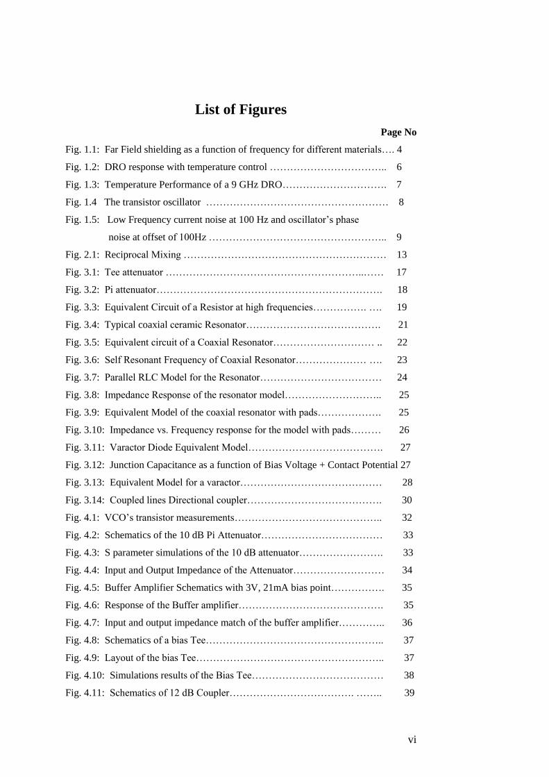
Fig. 1.1: Far Field shielding as a function of frequency for different materials…. 4
Fig. 1.2: DRO response with temperature control …………………………….. 6
Fig. 1.3: Temperature Performance of a 9 GHz DRO…………………………. 7
Fig. 1.4 The transistor oscillator ……………………………………………… 8
Fig. 1.5: Low Frequency current noise at 100 Hz and oscillator’s phase
noise at offset of 100Hz …………………………………………….. 9
Fig. 2.1: Reciprocal Mixing …………………………………………………… 13
Fig. 3.1: Tee attenuator …………………………………………………..…… 17
Fig. 3.2: Pi attenuator…………………………………………………………. 18
Fig. 3.3: Equivalent Circuit of a Resistor at high frequencies……………. …. 19
Fig. 3.4: Typical coaxial ceramic Resonator…………………………………. 21
Fig. 3.5: Equivalent circuit of a Coaxial Resonator………………………… .. 22
Fig. 3.6: Self Resonant Frequency of Coaxial Resonator………………… …. 23
Fig. 3.7: Parallel RLC Model for the Resonator……………………………… 24
Fig. 3.8: Impedance Response of the resonator model……………………….. 25
Fig. 3.9: Equivalent Model of the coaxial resonator with pads………………. 25
Fig. 3.10: Impedance vs. Frequency response for the model with pads……… 26
Fig. 3.11: Varactor Diode Equivalent Model…………………………………. 27
Fig. 3.12: Junction Capacitance as a function of Bias Voltage + Contact Potential 27
Fig. 3.13: Equivalent Model for a varactor…………………………………… 28
Fig. 3.14: Coupled lines Directional coupler…………………………………. 30
Fig. 4.1: VCO’s transistor measurements…………………………………….. 32
Fig. 4.2: Schematics of the 10 dB Pi Attenuator……………………………… 33
Fig. 4.3: S parameter simulations of the 10 dB attenuator……………………. 33
Fig. 4.4: Input and Output Impedance of the Attenuator……………………… 34
Fig. 4.5: Buffer Amplifier Schematics with 3V, 21mA bias point……………. 35
Fig. 4.6: Response of the Buffer amplifier……………………………………. 35
Fig. 4.7: Input and output impedance match of the buffer amplifier………….. 36
Fig. 4.8: Schematics of a bias Tee…………………………………………….. 37
Fig. 4.9: Layout of the bias Tee……………………………………………….. 37
Fig. 4.10: Simulations results of the Bias Tee………………………………… 38
Fig. 4.11: Schematics of 12 dB Coupler………………………………. …….. 39

vii
Fig. 4.12: Response of the 12 dB Coupler……………………………………. 40
Fig. 4.13: Schematics of the Voltage Controlled Oscillator …………………. 41
Fig. 4.14: Layout of the Voltage Controlled Oscillator………………………. 41
Fig. 4.15: OscTest Response of the Oscillator………………………………... 42
Fig. 4.16: PCB of the VCO…………………………………………................ 44
Fig. 4.17: VCO measurements through Spectrum Analyzer…………………. 45
Fig.4.18: Load Pull measurements …………………………………………... 47
Fig. 5.1: Schematics for Matching Network of the Buffer Amplifier………... 49
Fig. 5.2: Results of the Matching Network of Buffer Amplifier……………... 50
Fig. 5.3: Recommended pad for the Resonator………………………………. 50
Fig. 5.4: Resonator with Pads, One Port Test circuit………………………… 51
Fig. 5.5: One Port Measurements of the Resonator………………………….. 51

viii
List of Tables
Page No
Table 1.1: Phase Locked DRO/CRO Performance ………………………………… 2
Table 1.2: Properties of Shielding Materials …………………………………….. 3
Table 2.1: Center Frequency, Tuning range (absolute and relative)
for different standards ……………………………………………….. 14
Table 4.1: Oscillation Frequency of VCO as a function of varactor bias voltage … 43
Table 4.2: Results of the VCO for the Varactor tuning………………………….. 45
Table 4.3: Results of the VCO over a Temperature Range……………………… 46
Table 5.1: Tuning range results with varying capacitor values………………….. 48

1
Chapter 1 Introduction
1.1 Introduction
This Masters Degree Project is a study, design and implementation of a C band
microwave oscillator for the C band transceiver, used in wave radar. The most
important parameters affecting the microwave oscillator design are studied which
include the tuning range, shielding of the oscillator circuits, temperature performance
and frequency instability due to load and supply pulling.
A state of the art phase locked DRO/CRO is described, mainly used in space
applications [1]. Previously the implementation of oscillators was realized using
crystal oscillator followed by a chain of multipliers for good stability and phase noise.
The new approach is to use a Dielectric Resonator Oscillator (DRO) or a Coaxial
Resonator Oscillator (CRO). This approach provides very good long term stability,
better temperature performance and reduced sizes. The DRO or CRO is phase locked
to a temperature compensated crystal oscillator (TCXO). The main advantage of the
phase locked loop is that the crystal oscillator’s long term stability is inherited to the
DRO or CRO. The offset frequencies within the loop have the same phase noise and
bandwidth as that of the crystal oscillator. This eliminates the use of filters for
removing spurious harmonics. The resonators used, are made of dielectric materials.
These have a very high unloaded Q at microwave frequencies and are insensitive to
radiations which make them ideal for aerospace applications. The tuning of these
resonators is very simple as well. Overall the entire phase locked loop DROs and
CROs have shown good spurious and phase noise performance and are less
complicated. Table 1 shows some of the characteristic results of the B. Hitch and T.
Holden’s DRO and CRO implementations.

2
𝑷𝒆𝒓𝒇𝒐𝒓𝒎𝒂𝒏𝒄𝒆 𝑷𝒂𝒓𝒂𝒎𝒆𝒕𝒆𝒓 𝑷𝒉𝒂𝒔𝒆 𝑳𝒐𝒄𝒌𝒆𝒅 𝑪𝑹𝑶 𝑷𝒉𝒂𝒔𝒆 𝑳𝒐𝒄𝒌𝒆𝒅 𝑫𝑹𝑶
𝐹𝑟𝑒𝑞𝑢𝑒𝑛𝑐𝑦 𝑆𝑡𝑎𝑏𝑖𝑙𝑖𝑡𝑦 ± 1.5 𝑝𝑝𝑚 𝑎𝑙𝑙 𝑐𝑎𝑢𝑠𝑒𝑠 ± 1.5 𝑝𝑝𝑚 𝑎𝑙𝑙 𝑐𝑎𝑢𝑠𝑒𝑠
𝑃𝑎𝑠𝑒 𝑁𝑜𝑖𝑠𝑒
10 𝐻𝑧 −63 𝑑𝐵𝑐/𝐻𝑧 −63 𝑑𝐵𝑐/𝐻𝑧
100 𝐻𝑧 −94 𝑑𝐵𝑐/𝐻𝑧 −94 𝑑𝐵𝑐/𝐻𝑧
1 𝐾𝐻𝑧 −113 𝑑𝐵𝑐/𝐻𝑧 −113 𝑑𝐵𝑐/𝐻𝑧
10 𝐾𝐻𝑧 −117 𝑑𝐵𝑐/𝐻𝑧 −117 𝑑𝐵𝑐/𝐻𝑧
100 𝐾𝐻𝑧 −120 𝑑𝐵𝑐/𝐻𝑧 −128 𝑑𝐵𝑐/𝐻𝑧
Table 1.1: Phase Locked DRO and CRO performance [1]
The stability of signal source depends on maintaining the phase locked loop
conditions. The bandwidth requirements may force to use multiple narrowband
ceramic CROs. The spectral purity of these ceramic CROs is very good but they have
several disadvantages. These include limited temperature and tuning ranges. Another
disadvantage is that they are not suitable for integrated circuits (ICs) fabrication at the
present. Further more the ceramic resonators are sensitive to phase hits due to tension
in the crystal structure [2].
1.2 Susceptibility to Electromagnetic Fields and Shielding
Electronic circuits may be classified as shielding circuits, non-shielding circuits and
semi-shielding circuits each having different requirements for shielding in a
multilayer PCB. The three-dimensional configuration of the shielding circuits plays a
vital role in achieving a stable shielded structure [3]. The shielding may be electric,
magnetic or electromagnetic in nature.
The electromagnetic shield takes the form of an enclosure which consists of metal
plates and foils usually. The electromagnetic shield construction on the actual printed
board also determines its effectiveness. The two factors which increase the efficiency
of the electromagnetic shields are the electrical contact in the shield layer and making
the path longer for the leakage of the electromagnetic fields. This increases the
efficiency of the contact joints in electromagnetic shields [4].

3
The aerospace structures require a high degree of electromagnetic interference (EMI)
shielding, compared to other electronics structures. The weight of these shields is a
limiting factor, thus a high strength, high elastic modulus and light weight shields are
required with better EMI shielding abilities. Metallic shields are used currently which
have higher densities.
𝑴𝒂𝒕𝒆𝒓𝒊𝒂𝒍 𝑫𝒆𝒏𝒔𝒊𝒕𝒚
𝒈/𝒄𝒎𝟑
𝑹𝒆𝒔𝒊𝒔𝒕𝒊𝒗𝒊𝒕𝒚
𝝁𝛀 𝒄𝒎
𝑺𝒕𝒓𝒆𝒏𝒈𝒕𝒉
𝑴𝑷𝒂
𝑴𝒐𝒅𝒖𝒍𝒖𝒔
𝑮𝑷𝒂
Copper 8.96 1.78 420 110
Iron 7.86 10 200 200
Aluminum Alloy 2.80 10 520 71
Aluminum 2.70 2.82 210 60
Beryllium 1.85 4.0 620 290
P-100 + Br/epoxy 1.78 90 840 430
P-100/epoxy 1.72 460 840 430
T-300/epoxy 1.51 5000 3200 228
Table 1.2: Properties of shielding materials [5]
Table 1.2 describes some of the properties of the metallic and composite shielding
materials. The most commonly used and most effective shielding material is
aluminum, but it has a very high density. Carbon fibers are light weight, but not
having enough conductivity, which results in insufficient shielding. Paints, plating
and foils on the carbon composites may provide needed shielding, but there are issues
with reliability, scratching, low adhesion and they may oxidize in air.
The Fig. 1.1 describes the total far field shielding at different frequencies for different
materials. At low frequencies the attenuation is almost frequency independent, until
up to some characteristic value after which it increases sharply. The metals Cu and Al
provide the best shielding as the attenuation rises sharply after 105 Hz. The other
composites have low shielding at high frequencies, PAN having the least.

4
Fig. 1.1: Far Field shielding as a function of frequency for different materials [5]
The Al/Cu foil is very effective EMI shield. It is low cost and may be used with high
conductive adhesive. The EMI conductive coatings or adhesives on light weight
plastics is also becoming in use. These conductive paints are of many types such as
silver-copper paints, copper, nickel or silver paints etc [6].
The phase cancellation principle works in uniform magnetic materials at front face
providing up to 40 dB absorption per ounce. For 50-800 MHz frequency range, spinal
ferrites are used while for 800 MHz-2 GHz frequencies, ferroxplana is common. On
the contrary thick EMI shielding materials with a uniform dielectric does not follow
the phase cancellation principle due to their lossy conductor fibers where the
absorption is equivalent to the power loss. These have low densities and
permittivities. Comparing with ferrites, metals have higher permittivities at
microwave frequencies and are better EMI absorbers. The losses of the magnetic
absorbers are dependant on their magnetic fields so a non-conducting material is
desired. Dielectric absorbers require thick layers, where the relative permittivity is
desired close to one. Practically these absorbers have higher permittivities, so are not
appropriate in many cases [7].
5
Another problem in circuits is the low frequency Electromagnetic Pulse (EMP).
Filtering this EMP is usually achieved through proper isolation which is provided by
highly permeable ferrite shields. But in cases where there are large distances between
the wave impedance of the shield and the intrinsic impedance of the metal, a higher
reflection occurs for the impinging wave. Thus copper and aluminum are preferred
choices compared with ferrites in such conditions. It can be concluded that with low
frequencies and large separation between source of the signal and the shields, higher
conducting materials provides better shielding abilities [8].
1.3 Tuning Range
The tuning network plays a key role in defining the frequency range of an oscillator.
The tuning network consists mainly of the resonator whose type determines the
frequency of oscillation. The voltage controlled oscillator may have frequency output
at some specified frequency range. In general, higher the center frequency of the
oscillator, the more difficult the design is. Oscillators are analyzed usually over a
frequency range around the center frequency.
The MMIC varactor diode has a specific tuning range provided by the manufacturer.
The introduction of negative resistance connected to the varactor diode using an
active circuit increases the varactor’s tuning range more than 10 times. In wide band
VCOs, the frequency range relation 𝑓𝑚𝑎𝑥
𝑓𝑚𝑖𝑛 is proportional to the tuning range of the
varactor diode 𝐶𝑚𝑎𝑥
𝐶𝑚𝑖𝑛 . The negative capacitance can be created by two common
source transistors loaded with inductor [9].
1.4 Temperature Performance
The temperature variations affect the performance of the active devices and oscillator
as a whole. For oscillators, a working temperature range is defined and the change in
the output power of the oscillator is specified in that temperature range. The
simulations usually imply that the junction temperature is constant at 25𝑜𝐶. For this
oscillator design, a range of 0𝑜 − 60𝑜 C is specified.
6
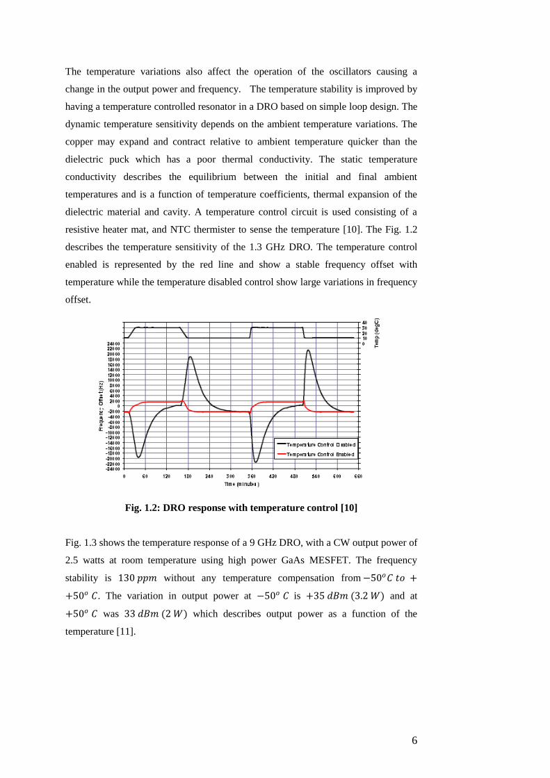
The temperature variations also affect the operation of the oscillators causing a
change in the output power and frequency. The temperature stability is improved by
having a temperature controlled resonator in a DRO based on simple loop design. The
dynamic temperature sensitivity depends on the ambient temperature variations. The
copper may expand and contract relative to ambient temperature quicker than the
dielectric puck which has a poor thermal conductivity. The static temperature
conductivity describes the equilibrium between the initial and final ambient
temperatures and is a function of temperature coefficients, thermal expansion of the
dielectric material and cavity. A temperature control circuit is used consisting of a
resistive heater mat, and NTC thermister to sense the temperature [10]. The Fig. 1.2
describes the temperature sensitivity of the 1.3 GHz DRO. The temperature control
enabled is represented by the red line and show a stable frequency offset with
temperature while the temperature disabled control show large variations in frequency
offset.
Fig. 1.2: DRO response with temperature control [10]
Fig. 1.3 shows the temperature response of a 9 GHz DRO, with a CW output power of
2.5 watts at room temperature using high power GaAs MESFET. The frequency
stability is 130 𝑝𝑝𝑚 without any temperature compensation from −50𝑜𝐶 𝑡𝑜 +
+50𝑜 𝐶. The variation in output power at −50𝑜 𝐶 is +35 𝑑𝐵𝑚 (3.2 𝑊) and at
+50𝑜 𝐶 was 33 𝑑𝐵𝑚 (2 𝑊) which describes output power as a function of the
temperature [11].

7
Fig. 1.3: Temperature performance of a 9 GHz DRO [11]
1.5 Frequency Pulling due to Load
The load variations affect the frequency of the voltage controlled oscillator (VCO).
The variation in the output impedance affects the DC voltages of the VCO’s
transistor. The BJT (Bipolar Junction Transistor) has supply voltages for different
junctions that must be constant throughout the operation of the oscillator. A change in
the Base-Collector voltage (𝑉𝐶𝐵) is caused by the change in the VCO’s output Base-
Collector capacitance. This varies the frequency of oscillation to a large value. Load
pulling is minimized by using a very high isolation stage between the load and VCO.
Frequency Pulling is a measure of the shift in frequency for a unity VSWR load
(usually 50 ohms) to the non-unity VSWR due to change in the load.
The load pulling measurements are done using variable transmission line and a load
impedance which is not matched. The VCO and load are connected together. The
transmission line is used for varying the phase angle between the load and VCO
between 0𝑜 − 360𝑜 . In this way the frequency variations due to the load variations
are measured.

8
A very linear MIC bipolar VCO with 100 MHz FM rate is described where the
frequency pulling is ± 1 𝑀𝐻𝑧 into a 2:1 mismatched load. The power flatness and
immunity from load pulling is achieved by using a two stage GaAs FET buffer
amplifier. The total load isolation achieved is more than 45 dB. The FET amplifier
provides 35 dB of isolation while 12 dB of isolation is provided by a thin film pi
attenuator [12].
1.6 Frequency Pulling due to Supply
The frequency of the VCO is affected by the supply voltage to some extent. In
transceiver systems, power amplifier uses a lot of the power and turning it on, will
increase the current drastically, which may affect the LO power supply and the VCO
frequency will increase. This can be minimized by isolating the VCO unit from the
power amplifier unit. The battery supply voltage drops to a certain minimum during
its life time and the oscillator design should work in a certain range of voltage. This
may be indicated in terms of tolerance as well for example ±10 % of 3 𝑉 power
supply. Temperature also affects the supply voltage bias. Noise on the supply voltage
lines causes noise and spurious on the oscillator.
The external environmental conditions like temperature or supply voltage variations
affect the active elements of the microwave oscillators thus inducing frequency
instability. The two reasons for this instability are variations in the cut off frequency
and collector capacitance. For the analysis, a simple tuned circuit is chosen as a
passive frequency determining network while a common base configuration is
selected for the active element as seen in Fig. 1.4.
Fig. 1.4 The transistor oscillator [13]
9
The high frequency analysis shows that the two most important parameters of the
reactive elements of the transistor are the collector capacitance and the frequency
dependence of the current gain. Variations in these factors give rise to variations in
the oscillation frequency. The collector capacitance is mainly a function of the
collector voltage. The relation between the changes in collector capacitance 𝐶𝑐 and
Collector voltage 𝑉𝑐 for a typical p-n-p transistor is given in eq. 1.1.
𝜕 𝐶𝑐
𝐶𝑐= −
1
2 𝜕 𝑉𝑐
𝑉𝑐 (1.1)
The effective base width of the transistor depends on the collector voltage and hence
frequency of oscillation. The Ebers and Miller [14] equation for the relation between
the 𝑓𝑎 and 𝑉𝑐 is approximated as
𝑓𝑎
𝑓𝑎𝑜 = 1 + 𝐾𝑉𝐶 𝑓𝑎𝑜 (1.2)
where
𝑓𝑎𝑜 = 𝑇𝑒 𝑣𝑎𝑙𝑢𝑒 𝑜𝑓 𝑓𝑎𝑓𝑜𝑟 𝑧𝑒𝑟𝑜 𝑉𝑐
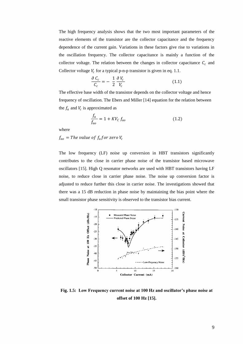
The low frequency (LF) noise up conversion in HBT transistors significantly
contributes to the close in carrier phase noise of the transistor based microwave
oscillators [15]. High Q resonator networks are used with HBT transistors having LF
noise, to reduce close in carrier phase noise. The noise up conversion factor is
adjusted to reduce further this close in carrier noise. The investigations showed that
there was a 15 dB reduction in phase noise by maintaining the bias point where the
small transistor phase sensitivity is observed to the transistor bias current.
Fig. 1.5: Low Frequency current noise at 100 Hz and oscillator’s phase noise at
offset of 100 Hz [15].

10
The Fig. 1.5 shows the measured and predicted results and are calculated based on
curve fitted LF noise. The experimental results predicts that the residual phase noise
of the HBT based oscillators is a function of the bias dependant LF noise up
conversion factor of the device. This concludes that for a low phase noise, the two
important decisions are device selection and matching network design.
The variations in supply voltage could cause a change in the output power of the
microwave oscillator. The output power can be controlled for microwave oscillators
by varying the bias voltage of the active element while using the scheme with a
synchronized oscillator. The results from the theoretical and experimental
investigations proves that a change of 0.2 V or 2.7 % of bias voltage change may
cause an output power change of up to 40 dB, with frequency being the constant
factor [16].
1.7 Thesis Outline
Chapter 2 describes the theory of the oscillator design. The different types of
oscillator topologies are described. There is a discussion of the oscillator properties,
characteristics and limitations.
Chapter 3 describes the design strategies of the VCO and the sub circuits used in it.
These sub circuits include the attenuator, buffer amplifier, resonator, and varactor
tuning network, coupler etc.
Chapter 4 consists of the simulations, results and fabrication of the VCO. The
expected results are analyzed to the measured results.
Chapter 5 describes the conclusions, discussions, week points and probable solutions
to these problems. It also includes a comparative study of this project results with the
state of the art work done by the others.
Chapter 6 gives an idea of the future work to be done in this design.

11
Chapter 2 Theory
2.1 Theory of Oscillators
An oscillator is a non linear circuit which transforms DC power to an AC waveform.
This circuit usually consists of an amplifier, a resonator and a feedback network. The
feedback may be internal i.e. a part of energy from the active device is fed back to the
resonator or it may be an external feedback circuit.
The active device in the oscillator takes in DC power from a regulated supply and for
an input power gives a specific output power which is several times higher in
magnitude. It can be a bipolar junction transistor (BJT), or a field effect transistor
(FET) or a Gain block which is usually wideband.
The specifications affecting the quality of operation of the whole system depends on
the cleanliness of the oscillator signal i.e. low phase noise and low spurious, which
constitute noise in systems. The desired characteristics for oscillators are sufficient
output RF power level, low phase noise, efficiency and stability of the signal etc.
Several noises contribute to the total noise of the oscillator. These include losses in
the resonator, transistor noise, noises modulated in power supply and noise due to the
varactor diode tuning.
2.2 Microwave Oscillator Configurations
There are three types of approaches for designing oscillators.
In one port oscillators, the transistor and the feedback network is replaced by a
negative resistance. For example, in Colpitt and Clapp oscillators, the capacitive
feedback creates a negative resistance along the tuning network.
In two port oscillators, the transistor acts as a two port device with its third terminal
grounded. The tuning network is used for the feedback which determines the
frequency. Such oscillators have a specific gain, phase shift, resonator network and
matching network.

12
Three port oscillators have an inductor at the base with some capacitance at the output
port. This feedback configuration generates negative resistance at input and output
port.
2.3 Voltage Controlled Oscillators
Voltage controlled oscillators or simply VCOs are the class of oscillators in which the
frequency determining reactance is varied by voltage. For high frequency
applications, the voltage controlled element is a typical varactor diode.
The VCOs find its use in many important applications such as function generators,
transmitters of every kind, frequency synthesizers and almost every type of wireless
communication equipment.
2.4 Considerations in Oscillators
2.4.1 Phase Noise
Phase noise is measured as dBc in a bandwidth of 1 Hz at an offset of a specific
frequency. There are several types of noises and spurious which modulate the output
signal of the VCO on either sides of the carrier.
Phase noise is short term phenomenon and some of the possible causes of phase noise
due to improper isolation are
Variations in the impedance of load
Mismatch reflections back to the VCO’s output
Rise in ground current
Coupling of radiations from nearby layout circuits
Changes in the bias supply of the VCO transistor due to load variations
The loaded Q is mainly responsible for the phase noise performance [17].
2.4.2 Harmonic Suppression
The typical harmonic suppression of a voltage controlled oscillator is about 15 dB, but
for certain systems, a very low harmonic content is desired. This can be achieved by
placing a microstrip low pass filter at the output.

13
2.4.3 Spurious signals in the Oscillator Output
Apart from harmonics, unwanted signals found on the sides of the carrier of an
oscillator are called spurious. A spurious free range is usually specified in terms of
dB. The synthesizer signals may be a cause for the generation of these spurious.
2.4.4 Post-tuning Drift
The tuning network which is a varactor diode is biased with supply voltage. After the
supply voltage has been applied, the frequency of the oscillator still drifts for some
time. This drift can affect the voltage controlled oscillators tuning speed.
2.4.5 Blocking or Reciprocal Mixing
The mixing of the local oscillator noise sidebands with the incoming strong signals is
called reciprocal mixing or blocking. This mixing produces unwanted noise at the
intermediate frequency. Fig. 2.1 shows the carrier signal A´ of the oscillator mixes
with the wanted signal A. The side bands of the oscillator B´, C´, D´ mixes with the
undesired signals A, B, C and creates interference in the intermediate frequency IF.
This affects considerably the receiver selectivity of increasing the noise floor.
Fig. 2.1 Reciprocal Mixing [18]

14
2.4.6 Linear Tuning characteristics
A linear relationship is desired for the variations in the frequency of the oscillator,
caused by varying the tuning voltage. This is an important factor for the stability of
synthesizers. Table 2.1 shows some standards for wireless communications. The
center frequency and tuning range (absolute and relative) is given for each standard.
The absolute tuning range shows the minimum and maximum frequencies while
relative tuning describes the percentage of the center frequency. The relative tuning
ranges for TV receiver, Satellite TV front end and DVB-T and FM radio front end are
very high. The GSM and UMTS relative ranges are narrow band with just around 3%.
The SONET standards are for fixed bit rates and only the center frequency is
indicated.
Table 2.1 Center Frequency, Tuning range (absolute and relative) for
different Standards [19]
The oscillator design requires a tuning range of about 80-100 MHz around the center
frequency.
2.5 Choice of the Active Device and Modeling
The two main choices available are FET and bipolar transistors. The transition
frequency and flicker noise corner frequency are important while choosing the active
device for the oscillator.

15
The frequency of transition 𝑓𝑇 of a transistor plays an important role in defining its
frequency of oscillation. The bipolar transistors have a 𝑓𝑇 of up to 25 GHz where as
SiGe based transistors have higher values of 𝑓𝑇 upto 100 GHz. The improved GaAs
based bipolar transistors called Heterojunction bipolar transistors (HBTs) have 𝑓𝑇 of
about 100 GHz also but it costs much more than silicon based transistors.
The flicker noise frequency of HBTs is higher than the SiGe transistors but it is not
prominent in practical circuits which have high lossy transmission media. Thus the
total oscillator noise in SiGe transistors and HBTs remains almost the same.
2.6 Loaded Q
The Loaded Quality factor of an oscillator is
𝑄𝐿 = 2𝜋 𝑇𝑜𝑡𝑎𝑙 𝑒𝑛𝑒𝑟𝑔𝑦 𝑠𝑡𝑜𝑟𝑒𝑑 𝑖𝑛 𝑡𝑒 𝑠𝑦𝑠𝑡𝑒𝑚(𝑖𝑛 𝑜𝑛𝑒 𝑓𝑢𝑙𝑙 𝑐𝑦𝑐𝑙𝑒)
𝐸𝑛𝑒𝑟𝑔𝑦 𝑙𝑜𝑠𝑡 𝑖𝑛 𝑡𝑒 𝑠𝑦𝑠𝑡𝑒𝑚 𝑖𝑛 𝑒𝑎𝑐 𝑐𝑦𝑐𝑙𝑒
In steady state, the external source supplies the energy to be lost.
The high loaded Q has certain advantages.
The high loaded Q reduces the frequency drift as resonator becomes the sole
frequency determining component.
The isolation of the resonator from the active device reactance minimizes the
effect of temperature.
The long term stability and phase noise performance is improved.

16
Chapter 3 Method
3.1 Passive Attenuator Design
Attenuator is a circuit which reduces the power of an incoming signal without the
significant distortion of the signal waveform and attenuation is expressed in 𝑑𝐵. The
main purpose of the attenuator, in combination with a buffer amplifier, is that the
proper output signal level is maintained at the VCO’s output and thus valuable reverse
isolation is achieved.
The VSWR values are of critical importance in the design of attenuators with resistive
elements. The attenuator is also used to improve the input match of the amplifier. This
may decrease the VSWR ratio at the input of the buffer amplifier and improve gain.
On the other side, every dB of attenuation at the input of the buffer amplifier increases
the Noise Figure (NF) of the amplifier.
The desirable characteristics of attenuators are reliability at the frequency of operation
and power applied to it. The attenuator design is usually achieved with the help of
resistors. The resistors used are usually surface mount. Since the output power from
the VCO transistor is few milliwatts, thus it doesn’t affect the device performance a
lot due to heating considerations.
Low Standing Wave Ratio (SWR) at input and output of the attenuator is always
desired. The low SWR at input and output can be achieved by careful design of the
attenuator circuit usually by having a symmetrical network. The SWR of the
attenuator and the input and output networks will contribute to the mismatch. This
variation is frequency dependant and it may degrade the flatness response of the
attenuator. The SWR at the input of attenuator may not be very important as VCO
transistor’s output is loaded with the attenuator to maintain the negative resistance
region. But at the output, a stable SWR is required to have the required reverse
isolation and matching. [20]
There are several topologies for achieving the attenuation in circuits. The passive
techniques i.e. Tee and Pi configurations are described here.

17
3.1.1 Tee Attenuator
Fig. 3.1 shows the Tee attenuator configuration and consists of two resistors of the
same value which are the series R1 & R2 resistors.
Z in Z out
R 1 R 2
R 3
Fig. 3.1: Tee attenuator
The resistances R1, R2 and R3 are calculated as
𝑅3 = 1
2 10
𝐿
10 − 1
𝑍𝐼𝑁 𝑍𝑂𝑈𝑇
10 𝐿
10
(3.1)
𝑅2 = 1
10 𝐿
10
+ 1
𝑍𝑂𝑈𝑇 (10 𝐿
10 − 1)
− 1𝑅3
(3.2)
𝑅1 = 1
10 𝐿
10
+ 1
𝑍𝐼𝑁 (10 𝐿
10 − 1)
− 1𝑅3
(3.3)
where
L = desired attenuation expressed in dB
𝒁𝑰𝑵 = desired Input impedance expressed in ohms
𝒁𝑶𝑼𝑻 = desired Output impedance expressed in ohms

18
3.1.2 Pi Attenuator
Fig. 3.2 shows the Pi attenuator configuration consisting of two resistors of the same
value i.e. R1and R2.
Z in Z out
R 1 R 2
R 3
Fig. 3.2: Pi attenuator
The resistances R1, R2 and R3 are calculated as
𝑅3 = 2 𝑍𝐼𝑁 𝑍𝑂𝑈𝑇 10
𝐿
10
10 𝐿
10 − 1
(3.4)
𝑅2 = 10
𝐿
10
+ 1
10 𝐿
10 − 1
𝑍𝑂𝑈𝑇 − 𝑅3 (3.5)
𝑅2 = 10
𝐿
10
+ 1
10 𝐿
10 − 1
𝑍𝐼𝑁 − 𝑅3 (3.6)
In terms of transducer gain which is equal to the attenuation of the attenuator
𝐴𝑡𝑡𝑒𝑛𝑢𝑎𝑡𝑖𝑜𝑛 = 𝑆21 2
3.2 Resistive Elements Models
The attenuator at low frequency can be designed using simple formulas as the
resistors act as lumped components. The resisters at high frequency have different
behavior at different frequencies and depend on a number of processes like the type of
resistors selected, accurate models for those resistors, accurate pads etc.

19
The factors affecting the modeling of the resistors at high frequencies are [21]
Dimensions of the resistor (Length, width, height etc.)
Skin Effect
Ground plan layout
The electrical length of the resistor relative to quarter wavelength
(approximately 1/10)
Components at high frequencies behave as non-ideal. For example the capacitor leads
have significant inductance while inductors have some self-capacitance. The Q of the
inductors is also considerable along with the parasitics due to coupling between
inductors. These parasitics should be considered in design and simulations. There are
parasitics associated with amplifiers as well. Thus the real world resistor acts as a
distributed component at high frequencies. Proper modeling of the resistors and other
components make them behave as lumped even at very high frequencies.
Fig. 3.3 shows the equivalent circuit of a resistor at high frequency, with a parasitic
inductance 𝐿𝑆 in series and parallel capacitance 𝐶𝑃. The parasitic reactance is
dependant upon the dimensions and mounting techniques of the resistors. The
inductance is usually just a few 𝑛𝐻 while the capacitance is a fraction of a pF.
Fig. 3.3 Equivalent Circuit of a Resistor at high frequencies
3.3 Buffer Amplifier
The component selected for providing the reverse isolation and amplification, in the
oscillator, is a low noise amplifier. It is Avago’s MGA-665P8 GaAs MMIC. It has a
unique active power down function. The features of this gain block are high gain, low
noise Figure and very high reverse isolation. It is incorporated in LPCC package
suitable for surface mounting. This improved performance is based on the Avago’s

20
state of the art E-HEMT (Enhancement Mode Pseudomorphic High Electron Mobility
Transistor).
There is a very good isolation between the output and input of the two stage MGA-
665P8 amplifier. It has a very low 𝑆22 i.e. −21.83 𝑑𝐵 while 𝑆12 is −37.72 𝑑𝐵, at 5.8
GHz. Thus there is a very good output match at the output. At the input, 𝑆21 is
15.99 𝑑𝐵 while 𝑆11 is −5.5 𝑑𝐵, at 5.8 GHz. Since the gain of the amplifier is very
high and a very high reverse isolation is present, thus no impedance matching is used
in the design. The buffer amplifier consists of two stages of amplifiers, each requiring
a separate bias. The pin 6 is supplied directly with the bias while the pin 7 is supplied
with a bias fed through a Bias Tee.
3.4 Resonator Network
The frequency of resonance determines the type of resonator used. For low
frequencies, lumped resonators are used while at higher frequencies, coaxial, ceramic,
microstrip resonators are commonly used. It also determines the phase noise
performance of the oscillator.
Fig. 3.4 shows a ceramic resonator with outer square cross section and inner
cylindrical shape. The W and 𝑙 are the width and length of the outer conductor while d
is the inner conductor diameter.
The approximate characteristic impedance of the coaxial line resonator is
𝑍𝑜 = 60
휀𝑟ln 1.08
𝑊
𝑑 (3.7)
The 𝑅𝑜 is usually between 5- 15 ohms while 휀𝑟 is from 10 to 100. This reduces the
size of the length of these resonators and is suitable for many applications including
spacecrafts.
𝜆𝑒𝑓𝑓 = 𝜆𝑓𝑟𝑒𝑒
휀𝑟 (3.8)
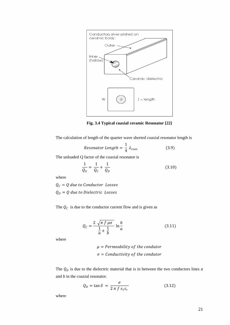
21
Fig. 3.4 Typical coaxial ceramic Resonator [22]
The calculation of length of the quarter wave shorted coaxial resonator length is
𝑅𝑒𝑠𝑜𝑛𝑎𝑡𝑜𝑟 𝐿𝑒𝑛𝑔𝑡 = 1
4 𝜆𝑐𝑜𝑎𝑥 (3.9)
The unloaded Q factor of the coaxial resonator is
1
𝑄𝑈=
1
𝑄𝐶+
1
𝑄𝐷 (3.10)
where
𝑄𝐶 = 𝑄 𝑑𝑢𝑒 𝑡𝑜 𝐶𝑜𝑛𝑑𝑢𝑐𝑡𝑜𝑟 𝐿𝑜𝑠𝑠𝑒𝑠
𝑄𝐷 = 𝑄 𝑑𝑢𝑒 𝑡𝑜 𝐷𝑖𝑒𝑙𝑒𝑐𝑡𝑟𝑖𝑐 𝐿𝑜𝑠𝑠𝑒𝑠
The 𝑄𝐶 is due to the conductor current flow and is given as
𝑄𝐶 =2 𝜋 𝑓 𝜇𝜍
1𝑎 +
1𝑏
ln𝑏
𝑎 (3.11)
where
𝜇 = 𝑃𝑒𝑟𝑚𝑒𝑎𝑏𝑖𝑙𝑖𝑡𝑦 𝑜𝑓 𝑡𝑒 𝑐𝑜𝑛𝑑𝑢𝑡𝑜𝑟
𝜍 = 𝐶𝑜𝑛𝑑𝑢𝑐𝑡𝑖𝑣𝑖𝑡𝑦 𝑜𝑓 𝑡𝑒 𝑐𝑜𝑛𝑑𝑢𝑡𝑜𝑟
The 𝑄𝐷 is due to the dielectric material that is in between the two conductors lines a
and b in the coaxial resonator.
𝑄𝐷 = tan 𝛿 = 𝜍
2 𝜋 𝑓 휀1휀𝑟 (3.12)
where
22
𝜍 =1
𝜌= 𝐶𝑜𝑛𝑑𝑢𝑐𝑡𝑖𝑣𝑖𝑡𝑦 𝑜𝑓 𝑡𝑒 𝐷𝑖𝑒𝑙𝑒𝑐𝑡𝑟𝑖𝑐
휀𝑟 = 𝑅𝑒𝑙𝑎𝑡𝑖𝑣𝑒 𝑃𝑒𝑟𝑚𝑖𝑡𝑡𝑖𝑣𝑖𝑡𝑦
휀𝑜 = 𝑃𝑒𝑟𝑚𝑖𝑡𝑡𝑖𝑣𝑖𝑡𝑦 𝑜𝑓 𝑡𝑒 𝑓𝑟𝑒𝑒 𝑠𝑝𝑎𝑐𝑒 = 8.854 × 10⁻¹² 𝐹 𝑚−1
A cylindrical coaxial resonator with inner conductor diameter d and outer conductor
diameter W. The equivalent circuit of this coaxial resonator is a parallel RLC circuit
as given in Fig. 3.5. The coaxial resonator is plated with silver plating.
R C L
Fig. 3.5 Equivalent circuit of a Coaxial Resonator
The unloaded Q for this coaxial resonator is
𝑄𝑈 = 𝑘 𝑓𝑜 ln(1.079
𝑊𝑑
)
25.4(1𝑊 +
1𝑑
) (3.13)
where
𝑊 = 𝑂𝑢𝑡𝑒𝑟 𝑐𝑜𝑛𝑑𝑢𝑐𝑡𝑜𝑟 𝑑𝑖𝑎𝑚𝑒𝑡𝑒𝑟
𝑑 = 𝐼𝑛𝑛𝑒𝑟 𝑐𝑜𝑛𝑑𝑢𝑐𝑡𝑜𝑟 𝑑𝑖𝑎𝑚𝑒𝑡𝑒𝑟
𝑘 = 240 𝑓𝑜𝑟 𝑠𝑖𝑙𝑣𝑒𝑟𝑒𝑑 𝑑𝑖𝑒𝑙𝑒𝑐𝑡𝑟𝑖𝑐 𝑤𝑖𝑡 휀𝑟 = 38.6
𝑘 = 200 𝑓𝑜𝑟 𝑠𝑖𝑙𝑣𝑒𝑟𝑒𝑑 𝑑𝑖𝑒𝑙𝑒𝑐𝑡𝑟𝑖𝑐 𝑤𝑖𝑡 휀𝑟 = 88.5
The input impedance of the resonator is
𝑍𝐼𝑁 = 60
휀𝑟ln 1.079
𝑊
𝑑 (3.14)
The inductance L is
𝐿 = 𝑙 𝑍𝑜 8 휀𝑟
25.4 𝜋2 3 × 10⁸ (3.15)
where
𝑙 = 𝑝𝑦𝑠𝑖𝑐𝑎𝑙 𝑙𝑒𝑛𝑔𝑡 𝑜𝑓 𝑡𝑒 𝑐𝑜𝑎𝑥𝑖𝑎𝑙 𝑟𝑒𝑠𝑜𝑛𝑎𝑡𝑜𝑟 𝑖𝑛 𝑚𝑚

23
The Capacitance is
𝐶 = 𝑙 휀𝑟
25.4 × 2 × 3 × 108 𝑍𝑜 (3.16)
The resistance is
𝑅 =4 𝑍𝑜𝑄
𝜋 (3.17)
The characteristics of coaxial line resonators below resonance are, they are high Q
components and temperature stable and act as ideal inductor elements over a narrow
range of frequencies as seen in Figure 3.6. The coaxial resonator acts as a distributed
structure having capacitance and inductance. The line has a specific frequency at
which it resonate called Self Resonant Frequency (SRF). The line exhibits inductive
reactance when it is operated below the SRF while acts as capacitive if operated
above SRF.
Fig. 3.6 Self Resonant Frequency of Coaxial Resonator [23]
Compared to traditional coil resonators, the ceramic coaxial resonators have a number
of advantages
Their ruggedness makes it suitable for incorporating in PCBs.
They have a very good Q value
They have a better temparture stability perforamce
Immunity to microphonics

24
3.4.1 Modeling the Resonator
The CAD (Computer Aided Design) software used is Agilent ADS (Advanced Design
System). Since the manufacturer didn’t provide a specific CAD model for the
resonator, a model is established for this simulation purposes.
The quarter wave shorted coaxial resonator model can be realized by using the
parallel RLC circuit as below. The R, L and C values supplied by the manufacturer
are simulated in parallel RLC circuit as in Fig. 3.7.
Fig. 3.7 Parallel RLC Model for the Resonator
Fig. 3.8 shows the impedance response of the above model and it shows that the
impedance is highest at the 6.2 GHz frequency which is the frequency of oscillation.
Thus this model acts as specifications.

25
Fig. 3.8 Impedance Response of the resonator model
The manufacturer has its own recommended layout for the resonator pads as given in
Appendix B. The recommendations are followed and pads are added to the model as
shown in Fig. 3.9.
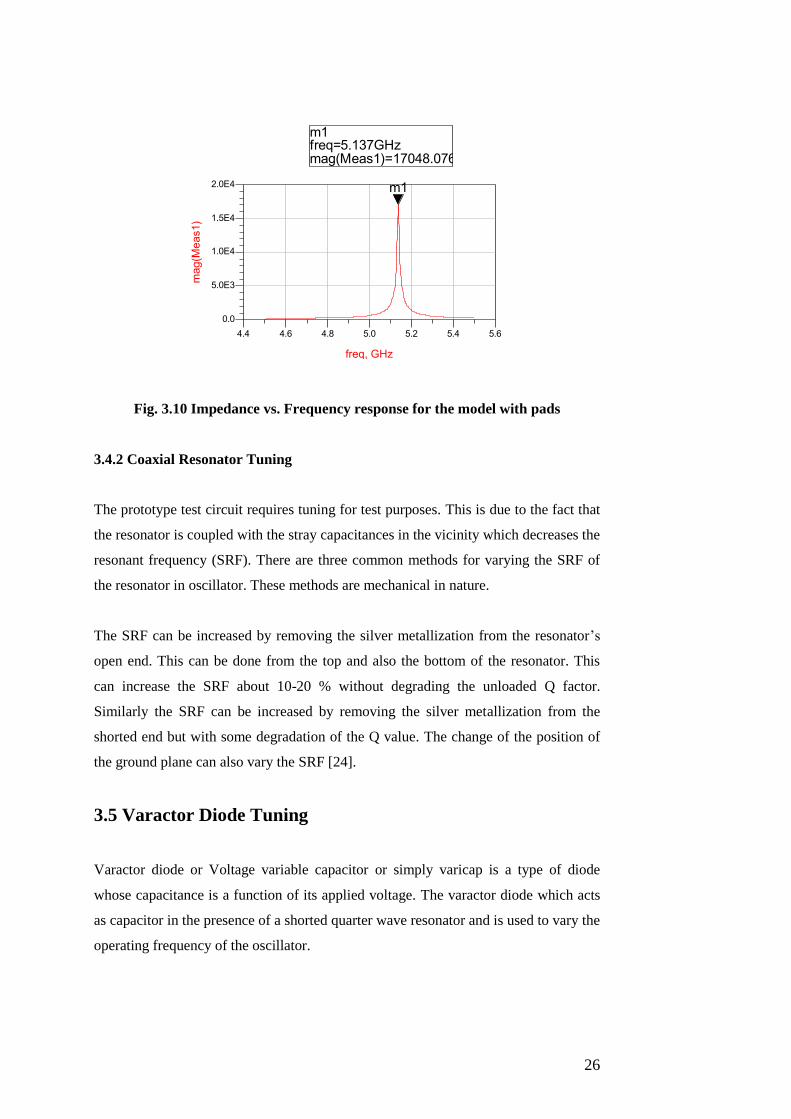
Fig. 3.9 Equivalent Model of the coaxial resonator with pads
This effectively changes the model supplied by the manufacturer. Fig. 3.10 shows that
the frequency is shifted and the new model oscillates at 5.137 GHz which is more
than one GHz below the frequency of the original model.
5.9 6.0 6.1 6.2 6.3 6.4 6.55.8 6.6
5.0E3
1.0E4
1.5E4
2.0E4
2.5E4
0.0
3.0E4
freq, GHz
mag(M
eas1)
Readout
m1
m1freq=mag(Meas1)=25641.000
6.200GHz
26
Fig. 3.10 Impedance vs. Frequency response for the model with pads
3.4.2 Coaxial Resonator Tuning
The prototype test circuit requires tuning for test purposes. This is due to the fact that
the resonator is coupled with the stray capacitances in the vicinity which decreases the
resonant frequency (SRF). There are three common methods for varying the SRF of
the resonator in oscillator. These methods are mechanical in nature.
The SRF can be increased by removing the silver metallization from the resonator’s
open end. This can be done from the top and also the bottom of the resonator. This
can increase the SRF about 10-20 % without degrading the unloaded Q factor.
Similarly the SRF can be increased by removing the silver metallization from the
shorted end but with some degradation of the Q value. The change of the position of
the ground plane can also vary the SRF [24].
3.5 Varactor Diode Tuning
Varactor diode or Voltage variable capacitor or simply varicap is a type of diode
whose capacitance is a function of its applied voltage. The varactor diode which acts
as capacitor in the presence of a shorted quarter wave resonator and is used to vary the
operating frequency of the oscillator.
4.6 4.8 5.0 5.2 5.44.4 5.6
5.0E3
1.0E4
1.5E4
0.0
2.0E4
freq, GHz
mag(M
eas1)
Readout
m1
m1freq=mag(Meas1)=17048.076
5.137GHz

27
Fig. 3.11 Varactor Diode Equivalent Model
Fig. 3.11 shows the varactor diode which is reverse biased for proper operation. A
small capacitor is also used in series with the varactor. This capacitor helps in
increasing the tuning range of the varactor.
The varactors may be built from Silicon and Gallium Arsenide (GaAs). Si is
economical for large scale production while GaAs provides higher Q values suitable
for high frequency applications. The advances in material gradient doping have paved
the way for improved processes. The abrupt junction is formed by the uniform
doping and is commonly used method. This provides an inverse square root
relationship which is considered as non linear.
The hyper abrupt junction provides a linear response over the frequency range by
varying the control voltage. These are narrowband in nature for linear region and the
Q is reduced, which imply that it can be used in lower frequency applications.
Fig. 3.12 Junction Capacitance as a function of Bias Voltage + Contact
Potential [25].

28
Fig. 3.12 shows the relationship of the junction capacitance and bias voltage along
with contact potential. With increase the control voltage of the varactor diode, the
capacitance of the varactor diode decreases and this shifts the oscillator’s frequency.
𝐴𝑏𝑟𝑢𝑝𝑡 𝐽𝑢𝑛𝑐𝑡𝑖𝑜𝑛 𝐶𝐽 𝑉𝑅 = 𝐴 = 𝐶𝑗𝑜
1 + 𝑉𝑅𝜙 𝛾 (3.18)
𝐹𝑟𝑒𝑞𝑢𝑒𝑛𝑐𝑦 𝐿𝑖𝑛𝑒𝑎𝑟 𝐶𝐽 𝑉𝑅 = 𝐹 = 𝐶𝑗𝑜
1 + 𝑉𝑅 𝛾
(3.19)
𝐻𝑦𝑝𝑒𝑟 𝐴𝑏𝑟𝑢𝑝𝑡 𝐽𝑢𝑛𝑐𝑡𝑖𝑜𝑛 𝐶𝐽 𝑉𝑅 = 𝐻 = 𝐶𝑗𝑜
1 + 𝑉𝑅𝜙
𝛾 (3.20)
where
𝛾 = 0.5 𝑓𝑜𝑟 𝑎𝑏𝑟𝑢𝑝𝑡 𝑗𝑢𝑛𝑐𝑡𝑖𝑜𝑛
𝛾 > 0.5 𝑓𝑜𝑟 𝐻𝑦𝑝𝑒𝑟 𝑎𝑏𝑟𝑢𝑝𝑡 𝑗𝑢𝑛𝑐𝑡𝑖𝑜𝑛
𝜙 = 𝐽𝑢𝑛𝑐𝑡𝑖𝑜𝑛 𝐶𝑜𝑛𝑡𝑎𝑐𝑡 ′𝑠 𝑃𝑜𝑡𝑒𝑛𝑡𝑖𝑎𝑙 = 0.7 𝑣 𝑓𝑜𝑟 𝑆𝑖 & 1.1 𝑣 𝑓𝑜𝑟 𝐺𝑎𝐴𝑠
𝐶𝑗𝑜 = 𝐷𝑖𝑜𝑑𝑒 𝑐𝑎𝑝𝑎𝑐𝑖𝑡𝑎𝑛𝑐𝑒 𝑎𝑡 𝑧𝑒𝑟𝑜 𝑣𝑜𝑙𝑡𝑠 𝑏𝑖𝑎𝑠 𝑣𝑜𝑙𝑡𝑎𝑔𝑒
𝑉𝑅 = 𝐴𝑝𝑝𝑙𝑖𝑒𝑑 𝑟𝑒𝑣𝑒𝑟𝑠𝑒 𝑏𝑖𝑎𝑠 𝑣𝑜𝑙𝑡𝑎𝑔𝑒
3.5.1 Mathematical Model for a varactor
The mathematical model of a varactor diode is described in Fig. 3.13. The variable
capacitance of the junction is 𝐶𝐽(𝑉) at applied voltage, while 𝑅𝑆(𝑉) is the series
resistance of the varactor diode. The diode has some constant parasitic capacitance 𝐶𝑃
as well due to packaging, dimensions of the diode and wiring. A parasitic inductance
is 𝐿𝑝 also present. The varactor diode is supplied with reverse bias voltage which
changes its capacitance and series inductance. This in turn changes the frequency
and/or phase of the electrical network.
Fig. 3.13 Equivalent Model of a Varactor Diode

29
3.5.2 Tuning Ratio of the Varicap
The tuning ratio is defined as the ratio in the capacitance between two values of the
applied reverse bias voltage.
𝑇𝑢𝑛𝑖𝑛𝑔 𝑅𝑎𝑡𝑖𝑜 = 𝐶𝑗 (𝑉2)
𝐶𝑗 (𝑉1)= (
𝑉1 + 𝜙
𝑉2 + 𝜙)𝛾 (3.21)
where
𝐶𝑗 𝑉1 = 𝐽𝑢𝑛𝑐𝑡𝑖𝑜𝑛 𝐶𝑎𝑝𝑎𝑐𝑖𝑡𝑎𝑛𝑐𝑒 𝑎𝑡 𝑣𝑜𝑙𝑡𝑎𝑔𝑒 𝑉1
𝐶𝑗 𝑉2 = 𝐽𝑢𝑛𝑐𝑡𝑖𝑜𝑛 𝐶𝑎𝑝𝑎𝑐𝑖𝑡𝑎𝑛𝑐𝑒 𝑎𝑡 𝑣𝑜𝑙𝑡𝑎𝑔𝑒 𝑉2
Provided that
𝑉1 > 𝑉2
3.5.3 Varactor in VCOs
The varactors are mainly used in VCOs for frequency tuning. The desirable
characteristics of varactors are
Minimum series resistance so that it does not affect the resonator Q
factor.
Less noise as its noise is added to the over all VCO noise
The appropriate tuning range and 𝐶 − 𝑉 characteristics [22]
3.6 Directional Coupler
The single section microstrip coupled line Directional Coupler consist of two
microstrip transmission lines close together. Due to this close proximity, the
electromagnetic energy or power is coupled between the lines.
Fig. 3.14 shows a microstrip directional coupler with four ports i.e. Input, transmitted,
coupled and isolated. One of the lines is termed as the “main line” which is between
port 1 and 2. This is the transmitted part where most of the power flows. The other
arm is called the coupled arm where a fraction of the input power is coupled. The
isolated port is terminated with matched impedance. The need for a coupler is to
divert some fraction of a power i.e. −10 𝑑𝐵 coupling in case of this oscillator, to the
synthesizer without interrupting much the main line power transfer.

30
Fig. 3.14 Coupled lines Directional coupler [26]
The microstrip coupler design and size depends on the choice of the substrate, height
of the substrate, dielectric permittivity, spacing between the coupled lines 𝑆, width of
the lines 𝑤 and length of the lines.
The directional coupler is linear and symmetrical in nature with the same width and
length of both the coupled lines so any port can be taken as the input port while the
port on the other side of the same arm is automatically the output. Similarly the
adjacent arm has the coupled and isolated ports. The coupled port provides the
frequency as well as a fraction of the power from the main line.
3.7 Bias Networks and Tees
There are three active semiconductor devices in the VCO’s design. These are the
VCO’s transistor, Buffer amplifier gain block and the varactor diode. All these require
a supply voltage which is fed through bias Tees.
The Bias Tee consists of a quarter wavelength transmission line which is about
7.8 𝑚𝑚 for the selected Rogers RO4003 substrate. Thus adding quarter wavelength of
line which is a short at the active device input will be open at quarter wave length
away. This is due to the fact that the quarter wavelength will move the short in is
Smith chart to open, 180 𝑜clockwise around the center of the smith chart. This
transforms the RF short circuit to RF open circuit at the other end of the quarter wave
line. The radial stub acts as a RF short and its DC open. The radial stub offers good
bandwidth compared to other stubs. Its isolates the RF from the bias tee and inducts
the DC freely.

31
3.8 Shielding
The requirements of shielding depend mainly on the use of the oscillator in a specific
application. For aerospace applications, the weight of the shield may be 10-15 % of
the total mass of the systems; a lighter shield is desired with good EMI shielding
abilities, high strength and high elasticity. In such cases metallic shields may not be
used and instead carbon composites/epoxies with some painting.
For this wave radar, the weight of the shield is not problem, as the radar is stationary
at some specific location, and the best shield may be selected which may be some
metallic shielding, like Aluminum, Copper etc. These Cu and Al have a very good
attenuation properties starting from 1 MHz and onward frequencies as in Fig. 1.1.
The metallic shielding is very efficient even in low frequency EMP. Since the shield
may be around the resonator and the oscillator circuit, so the distance is not very large
and ferrites may not be a better option than metallic shields as they are more
conductive.

32
Chapter 4 Process and Results
4.1 VCO’s Transistor Measurements
Fig. 4.1 displays the VCO’s transistor measurement test board. The transistor is
NEC’s NE685M03 and the configuration used is common base for the design of the
oscillator. The manufacturer does not provide a good model for up to 6 GHz
frequency with common base configurations, thus the measurements for the transistor
are carried out.
There is a radial stub at the base of the transistor for grounding. The measurements
are carried out through Vector Network Analyzer (VNA). The VNA is first calibrated
with Through Reflect Line (TRL) calibration method (See appendix C). The
measurement of the S parameters for the transistor with a radial stub at its base is
better characterized in this way. The transistor is supplied with a proper bias voltage.
Fig. 4.1 VCO’s transistor measurements
4.2 Attenuator Results
Fig. 4.2 shows the attenuator selected for the oscillator which is a symmetrical Pi
Network of resistors. The design is supplemented by the introduction of transmission
lines in between the resisters which are used to cancel out the reactance of the
resistors as the resisters are not perfect lumped components at very high frequencies.

33
Fig. 4.2 Schematics of the 10 dB Pi Attenuator
Fig. 4.3 S parameter simulations of the 10 dB attenuator
Fig. 4.3 shows the S parameter simulations of the 10 dB attenuator. The response is
over a frequency range of 4.8-6.8 GHz. The attenuation is with very good flatness of a
fraction of a dB over the entire frequency range. The attenuation of the attenuator i.e.
S(2,1) is 9.642 𝑑𝐵 which is close to 10 𝑑𝐵. Since the specifications of this
attenuation is very flexible, the difference of 0.4 𝑑𝐵 is not a problem at all. The S(1,2)
shows the reverse isolation of the attenuator and it is the same as S(2,1). This is due to
the fact that this design is a symmetrical Pi network.
5.0 5.2 5.4 5.6 5.8 6.0 6.2 6.4 6.64.8 6.8
-30
-20
-10
-40
0
freq, GHz
dB
(S(1
,2))
Readout
m1
dB
(S(2
,1))
dB
(S(1
,1))
Readout
m3
dB
(S(2
,2))
m1freq=dB(S(1,2))=-9.642
5.870GHz
m3freq=dB(S(1,1))=-37.311
5.870GHz
34
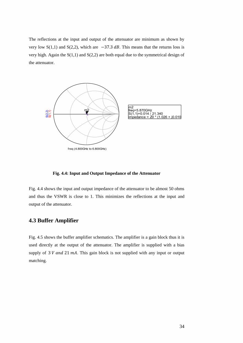
The reflections at the input and output of the attenuator are minimum as shown by
very low S(1,1) and S(2,2), which are −37.3 𝑑𝐵. This means that the returns loss is
very high. Again the S(1,1) and S(2,2) are both equal due to the symmetrical design of
the attenuator.
Fig. 4.4: Input and Output Impedance of the Attenuator
Fig. 4.4 shows the input and output impedance of the attenuator to be almost 50 ohms
and thus the VSWR is close to 1. This minimizes the reflections at the input and
output of the attenuator.
4.3 Buffer Amplifier
Fig. 4.5 shows the buffer amplifier schematics. The amplifier is a gain block thus it is
used directly at the output of the attenuator. The amplifier is supplied with a bias
supply of 3 𝑉 𝑎𝑛𝑑 21 𝑚𝐴. This gain block is not supplied with any input or output
matching.
freq (4.800GHz to 6.800GHz)
S(1
,1)
Readout
m2
S(2
,2)
m2freq=S(1,1)=0.014 / 21.340impedance = Z0 * (1.026 + j0.010)
5.870GHz

35
Fig. 4.5: Buffer Amplifier Schematics with 3V, 21mA bias point.
Fig. 4.6: Response of the Buffer amplifier
The Buffer amplifier response is shown in Fig. 4.6. The gain of the amplifier without
any input or output matching is about 16 dB. The most important parameter is the
reverse isolation of the amplifier S(1,2) which is −37.72 𝑑𝐵. This is the most
significant factor and very important for the oscillator along with the attenuator’s
reverse isolation. The others parameter S(2,2) is −22.14 𝑑𝐵 which is sufficient as
more than 20 𝑑𝐵 of return loss is always desirable. But the S(1,1) is just about
−5.2 𝑑𝐵 which is a bit too low.
5.0 5.2 5.4 5.6 5.8 6.0 6.2 6.4 6.6 6.84.8 7.0
-30
-20
-10
0
10
-40
20
f req, GHz
dB
(S(1
,1))
5.867G-5.271
m2
dB
(S(1
,2))
5.852G-37.72
m4
dB
(S(2
,1))
Readout
m1
dB
(S(2
,2))
5.874G-22.15
m3
nf(
2)
Readout
m7
m1freq=dB(S(2,1))=15.985
5.870GHz
m2freq=dB(S(1,1))=-5.261
5.870GHz
m3freq=dB(S(2,2))=-22.136
5.870GHz
m4freq=dB(S(1,2))=-37.721
5.870GHz
m7freq=nf(2)=1.688
5.876GHz

36
Fig. 4.7: Input and output impedance match of the buffer amplifier
The Input and output impedance match for the buffer amplifier is shown in Fig. 4.7.
The output impedance match is very good nearly 50 ohms but the input impedance
match is very poor. For the initial design, the Buffer Amplifier Gain block is used
without any input and output impedance match. This is due to the fact that the Buffer
amplifier has a very good gain of 16 dB without any matching circuit at the input or
output.
4.4 Power Supply Bias
The three active devices i.e. VCO’s transistor, varactor diode and the Buffer amplifier
is supplied with the proper bias voltage. The bias is supplied through bias tees and
Fig. 4.8 shows the schematics of bias tee. The bias tee consists of a quarter wave
transmission line which is about 7.8 mm on the Rogers 4003 substrate and a radial
stub. The layout of the bias tee is shown in Fig. 4.8.
freq (4.870GHz to 6.870GHz)
S(1
,1)
Readout
m6
S(2
,2)
Readout
m5
m6freq=S(1,1)=0.546 / -125.040impedance = Z0 * (0.365 - j0.464)
5.870GHz
m5freq=S(2,2)=0.078 / -140.330impedance = Z0 * (0.882 - j0.089)
5.870GHz

37
Fig. 4.8: Schematics of a Bias Tee
Fig. 4.9: Layout of the Bias Tee.

38
Fig. 4.10: Simulations results of the Bias Tee
The response of the bias tee is shown in Fig. 4.10. The S(2,1) is almost 0 dB which
implies that the high frequency signal is not affected by the bias Tee thus it passes
from port 1 to port 2 without any loss. The S(3,3) is also close to 0 dB which is port 3
is an RF Open and thus DC Short. Thus the RF signal will not enter the bias supply.
The value of -80 dB of the S(3,1) also confirms this. The reflections at port 1 are
minimum as S(1,1) is about -60 dB. Also at port S(1,1), the impedance is almost 50
ohms. This bias Tee is although not ideal but very much optimized and closer to ideal.
4.5 Coupler Design
The oscillator output is coupled with the synthesizer and the coupler is designed as in
Fig. 4.10. The coupler has four ports which are input, output, coupled and isolated.
The design is based on two microstrip lines coupled to each other. The isolated port is
terminated with matched impedance.
5.0 5.2 5.4 5.6 5.8 6.0 6.2 6.4 6.64.8 6.8
-0.08
-0.06
-0.04
-0.02
-0.10
0.00
freq, GHz
dB
(S(2
,1))
dB
(S(3
,3))
5.0 5.2 5.4 5.6 5.8 6.0 6.2 6.4 6.64.8 6.8
-60
-40
-80
-20
freq, GHz
dB
(S(1
,1))
dB
(S(3
,1))
Readout
m2
m2freq=dB(S(3,1))=-79.907
5.870GHzfreq (4.800GHz to 6.800GHz)
S(1
,1)
Readout
m1
S(3
,3)
S(3
,1)
m1freq=S(1,1)=0.008 / 95.719impedance = Z0 * (0.998 + j0.015)
5.780GHz
5.0 5.2 5.4 5.6 5.8 6.0 6.2 6.4 6.64.8 6.8
-100
0
100
-200
200
freq, GHz
ph
as
e(S
(3,1
))
Readout
m3
m3freq=phase(S(3,1))=-179.901
5.870GHz

39
Fig. 4.11: Schematics of 12 dB Coupler
The response of this coupler is given in Fig. 4.11. The coupled port has a coupling of
about 11.8 dB which is almost equal to 12 dB. The thru is -0.345 dB which depicts the
fact that most of the power is transmitted to the output port and only a small fraction
is sent to the coupled port. The directivity is -24.17 dB which is fairly good. The
Return loss is -29.9 dB thus there is very little reflections and the input port acts as a
matched port.

40
Fig. 4.12: Response of the 12 dB Coupler
Fig. 4.12 displays the voltage controlled coaxial resonator oscillator. The VCO’s
transistor is connected to the tuning network. The tuning network consists of the
coaxial resonator with one end shorted to ground. A varactor diode is also present in
the tuning network. The varactor and the resonator are connected through a tee and
are fed into the input of the VCO’s transistor. A 0.3 pF capacitor is also added along
the varactor diode.
4.0 4.5 5.0 5.5 6.0 6.5 7.0 7.53.5 8.0
-0.40
-0.35
-0.30
-0.25
-0.45
-0.20
freq, GHz
dB
(S(2
,1))
Readout
m1
Thru(dB)
m1freq=dB(S(2,1))=-0.345
5.870GHz
4.0 4.5 5.0 5.5 6.0 6.5 7.0 7.53.5 8.0
-13.5
-13.0
-12.5
-12.0
-11.5
-14.0
-11.0
freq, GHz
dB
(S(3
,1))
Readout
m2
Coupled Port(dB)
m2freq=dB(S(3,1))=-11.802
5.870GHz
4.0 4.5 5.0 5.5 6.0 6.5 7.0 7.53.5 8.0
-24
-23
-22
-21
-20
-25
-19
freq, GHz
dB
(S(3
,2))
Readout
m3
Directvity(dB)
m3freq=dB(S(3,2))=-24.170
5.870GHz
4.0 4.5 5.0 5.5 6.0 6.5 7.0 7.53.5 8.0
-30
-25
-20
-15
-35
-10
freq, GHz
dB
(S(1
,1))
dB
(S(2
,2))
Readout
m4
dB
(S(3
,3))
Return Loss(dB)
m4freq=dB(S(2,2))=-29.972
5.870GHz
freq (3.800GHz to 7.800GHz)
S(1
,1)
Readout
m5
m5freq=S(1,1)=0.031 / -141.241impedance = Z0 * (0.952 - j0.037)
5.870GHz

41
4.6 Voltage Controlled Oscillator (VCO) Circuit
The VCO circuit is shown in Fig. 4.13. A varactor is supplied with a variable bias
voltage which is used to tune the circuit. The VCO’s transistor is followed by an
attenuator of Pi shape. The attenuator is followed by the buffer amplifier and the
output is fed into the coupler. Fig. 4.14 displays the layout of the voltage controlled
oscillator. This layout is generated in Agilent ADS and does not include the voltage
bias circuits. This layout was imported in layout software “Mentor” and a PCB layout
was generated which contain all other components like the bias networks, connectors,
transmission lines etc.
Fig. 4.13: Schematics of the Voltage Controlled Oscillator
Fig. 4.14: Layout of the Voltage Controlled Oscillator

42
Fig. 4.15: OscTest Response of the Oscillator
These simulations are based on the OscTest component of Agilent ADS which
provides the S parameter analysis of the small signal gain (closed loop) for this
oscillator. The loop gain is represented by S(1,1) while it also measures the closed
loop phase. The oscillation is indicated by a loop gain of more than unity and the
phase at zero, while the frequency increase brings about a decrease in the phase.
5.0 5.2 5.4 5.6 5.8 6.0 6.2 6.4 6.64.8 6.8
1
2
3
4
0
5
-100
0
100
-200
200
freq, GHz
dB
(S(1
,1))
Readout
m1
phase(S
(1,1
))
Readout
m2
m1freq=dB(S(1,1))=3.716
5.570GHz
m2freq=phase(S(1,1))=-0.008
5.570GHz
-1.5 -1.0 -0.5 0.0 0.5 1.0 1.5-2.0 2.0
freq (4.800GHz to 6.800GHz)
S(1
,1)
Readout
m3
m3freq=S(1,1)=1.534 / -0.008
5.570GHz

43
The Agilent ADS simulations of the VCO are given in Fig. 4.15. The oscillator has
S(1,1) greater than unity at the 5.57 GHz while the phase at this frequency is almost
zero. Thus this is the oscillation frequency with a varactor bias voltage of 4 volts.
The Table 4.1 displays the results of simulations of the VCO. The varactor diode bias
voltage is selected from 4-18 volts with increments of 2 volts, which is the standard
operating voltage for Microsemi MPV2100 varactor diodes. The oscillation frequency
starts at 5.57 GHz at 4 volts of varactor voltage and reaches 5.636 GHz at a voltage of
18 volts. This gives a total tuning voltage of 80 volts.
Serial Number Varactor bias voltage
(volts)
Oscillation frequency
(GHz)
1 0 5.538
2 4 5.557
3 6 5.582
4 8 5.587
5 10 5.601
6 12 5.610
7 14 5.619
8 16 5.628
9 18 5.636
Table 4.1: Oscillation Frequency of VCO as a function of varactor bias voltage

44
4.7 Fabrications and Measurements
Fig. 4.16: PCB of the VCO
Fig. 4.16 shows the fabricated coaxial resonator oscillator. The results show that the
oscillator oscillates at 5.54 GHz in the absence of the 0.3 pF capacitor and the
varactor diode. This is almost very close to the designed frequency of oscillation. The
output power is 3.83 dBm measured though a spectrum Analyzer as shown in Fig.
4.17. It’s a bit lower than the expected 7 dBm for the specifications.
When the 0.3 pF capacitor is added with the resonator, the frequency of oscillation of
the VCO drops to 5.45 GHz while the output power is 4 dBm. Finally the varactor
diode is soldered and the results are obtained as in the Table 4.2.

45
Fig. 4.17: VCO measurements through Spectrum Analyzer
Serial Number Varactor bias
voltage
(volts)
Oscillation
frequency
(GHz)
Output Power
(dBm)
1 0 5.230 4
2 4 5.270 4
3 6 5.290 3.83
4 8 5.300 3.83
5 10 5.314 3.83
6 12 5.324 3.67
7 14 5.333 3.83
8 16 5.340 3.83
9 18 5.345 3.50
Table 4.2: Results of the VCO for the Varactor tuning
Table 4.2 show that the VCO has almost constant power of around 4 dBm. The tuning
range is 75 MHz which is good enough for the design.

46
𝑇𝑒𝑚𝑝 = 0𝑜𝐶 𝑇𝑒𝑚𝑝 = 20𝑜𝐶 𝑇𝑒𝑚𝑝 = 40𝑜 𝑇𝑒𝑚𝑝 = 60𝑜
S
No
.
𝑉𝑣𝑎𝑟
(𝑣𝑜𝑙𝑡𝑠)
𝑓𝑜
(𝐺𝐻𝑧)
𝑃𝑂𝑈𝑇
(𝑑𝐵𝑚)
𝑓𝑜
(𝐺𝐻𝑧)
𝑃𝑂𝑈𝑇
(𝑑𝐵𝑚)
𝑓𝑜
(𝐺𝐻𝑧)
𝑃𝑂𝑈𝑇
(𝑑𝐵𝑚)
𝑓𝑜
(𝐺𝐻𝑧)
𝑃𝑂𝑈𝑇
(𝑑𝐵𝑚)
1 4 5.285 4.17 5.279 3.67 5.271 3.67 5.254 3.13
2 6 5.300 4.33 5.292 3.67 5.283 3.67 5.274 3.33
3 8 5.313 4.17 5.305 3.83 5.295 4.00 5.284 3.13
4 10 5.327 4.33 5.317 4.17 5.305 3.5 5.293 3.13
5 12 5.337 4.17 5.328 4.17 5.314 3.67 5.305 3.5
6 14 5.346 4.00 5.337 4.17 5.325 3.84 5.312 3.5
7 16 5.354 3.53 5.345 4.00 5.334 3.83 5.319 3.5
8 18 5.357 4.00 5.347 3.83 5.337 3.83 5.340 3.67
Table 4.3 Results of the VCO over a Temperature Range
where
𝑓𝑜 = 𝑂𝑠𝑐𝑖𝑙𝑙𝑎𝑡𝑖𝑜𝑛 𝐹𝑟𝑒𝑞𝑢𝑒𝑐𝑛𝑦 𝑜𝑓 𝑡𝑒 𝑉𝐶𝑂 𝑒𝑥𝑝𝑟𝑒𝑠𝑠𝑒𝑑 𝑖𝑛 𝐺𝐻𝑧
𝑉𝑣𝑎𝑟 = 𝐵𝑖𝑎𝑠 𝑣𝑜𝑙𝑎𝑡𝑔𝑒 𝑎𝑝𝑝𝑙𝑖𝑒𝑑 𝑡𝑜 𝑡𝑒 𝑣𝑎𝑟𝑎𝑐𝑡𝑜𝑟 𝑑𝑖𝑜𝑑𝑒 𝑒𝑥𝑝𝑟𝑒𝑠𝑠𝑒𝑑 𝑖𝑛 𝑣𝑜𝑙𝑡𝑠
𝑃𝑂𝑈𝑇 = 𝑂𝑢𝑡𝑝𝑢𝑡 𝑝𝑜𝑤𝑒𝑟 𝑜𝑓 𝑡𝑒 𝑉𝐶𝑂 𝑒𝑥𝑝𝑟𝑒𝑠𝑠𝑒𝑑 𝑖𝑛 𝑑𝐵𝑚
Table 4.3 displays the temperature performance of the oscillator. The
temperature is selected from 0𝑜 to 60𝑜 which induces a shift of the frequency
about 30 MHz.
Phase Noise Measurements
The phase noise of this oscillator is −88 𝑑𝐵𝑚/𝐻𝑧 𝑎𝑡 50 𝑘𝐻𝑧 offset from
4 𝑑𝐵𝑚 carrier or −92 𝑑𝐵𝑐/𝐻𝑧. At 100 kHz offset the phase noise is
−94 𝑑𝐵𝑚/𝐻𝑧 ( −98 𝑑𝐵𝑐/𝐻𝑧).

47
Load Pull Measurements
Figure 4.1 shows the Load Pull measurement setup, with the DUT attached to
the cable having 1.5 dB loss, and a 3 dB attenuator. The attenuator is
connected to -10 dB approximately. The coupled port is connected to the
Spectrum Analyzer while the thru port is connected to the Line Stretcher
which is open circuit at other end.
Fig. 4.18: Load Pull measurements
The measurement shows that with a return loss of the setup equal to almost 12
dB, and with a change of phase from 0− 180𝑜 , a 1MHz of frequency pulling
is calculated.
The results were a bit different from the expected simulations. The biggest
cause was that the resonator layout was incorrectly perceived, and it pulled the
frequency about 300 MHz down from its target of 5.87 MHz. This was due to
incorrect layout realization due to which the exact frequency of 6.2 GHz was
not achieved. This calls for a need to make test circuits for the resonator and
the test it using one port VNA measurements. Thus the S Parameters obtained
this way can be used in the simulations.

48
Chapter 5 Discussions & Conclusions
Table 4.1 shows simulations of the varactor diode tuning and the resulting
frequency response in GHz. The varactor diode has an operating voltage range
from 4 to 18 volts. This will give a tuning range of
𝑇𝑢𝑛𝑖𝑛𝑔 𝑅𝑎𝑛𝑔𝑒 = 5.557 𝐺𝐻𝑧 − 5.636 𝐺𝐻𝑧 = 79 𝑀𝐻𝑧
The printed board measurements through a spectrum Analyzer showed the
tuning range as
𝑇𝑢𝑛𝑖𝑛𝑔 𝑅𝑎𝑛𝑔𝑒 = 5.270 𝐺𝐻𝑧 − 5.345 𝐺𝐻𝑧 = 75 𝑀𝐻𝑧
This shows a very good result of the tuning range as the 75-80 MHz tuning is
sufficient for the products at the company.
The capacitor in series with the varactor diode has a value of 0.3 pF in the VCO
design. This value is varied and some new results have been obtained as given in
Table 5.1. If this capacitor is not included, the OscTest S(1,1) phase is at zero but the
S(1,1) is not at maximum. In some cases the tuning range is very low if this capacitor
is not added. Thus the capacitor is added to the design. The value of the capacitor is
varied and results obtained in Table 5.1. These results show that the increase in the
capacitance increases the tuning range.
S. No Capacitor
(pF)
Frequency
(at 4 volts)
Frequency
(at 18 volts)
Tuning
frequency
range
1 0.1 5.765 5.775 10 MHz
2 0.2 5.664 5.694 30 MHz
3 0.3 5.574 5.634 60 MHz
4 0.4 5.493 5.574 81 MHz
5 0.5 5.433 5.544 111 MHz
Table 5.1 Tuning range results with varying capacitor values

49
There is another problem with this capacitor, as its value is too low i.e. 0.3 pF. The
high tolerance of this capacitor will increase the uncertainty. The parasitic reactance
could also be appreciable due to the manufacturing, soldering and mounting of the
components. Simulations have shown that increasing this capacitor value can increase
the tuning range but then a very high value capacitor value in the tuning network will
shift the oscillation frequency down which is not desirable. Thus a trade off was made
and a capacitor value was suggested and used.
The design of oscillator gave a low output power of around 3.5-4 dBm which is lower
than the expectations of the 7 dBm. In the previous design, no matching network was
used for the buffer amplifier although its input had a very bad match. Thus the input
of the buffer amplifier has to be matched with a matching network, to achieve a
higher gain.
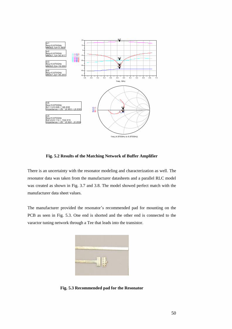
Fig. 5.1 shows that the input is matched and the gain of the amplifier is 17.5 dB which
is 1.5 dB higher. Also the Smith chart shows the input and output match to be around
50 ohms.
Fig. 5.1 Schematics for Matching Network of the Buffer Amplifier
50
Fig. 5.2 Results of the Matching Network of Buffer Amplifier
There is an uncertainty with the resonator modeling and characterization as well. The
resonator data was taken from the manufacturer datasheets and a parallel RLC model
was created as shown in Fig. 3.7 and 3.8. The model showed perfect match with the
manufacturer data sheet values.
The manufacturer provided the resonator’s recommended pad for mounting on the
PCB as seen in Fig. 5.3. One end is shorted and the other end is connected to the
varactor tuning network through a Tee that leads into the transistor.
Fig. 5.3 Recommended pad for the Resonator
5.0 5.2 5.4 5.6 5.8 6.0 6.2 6.4 6.6 6.84.8 7.0
-40
-30
-20
-10
0
10
-50
20
f req, GHz
dB
(S(1
,1))
Readout
m2
dB
(S(1
,2))
Readout
m4
dB
(S(2
,1))
Readout
m1
dB
(S(2
,2))
Readout
m3
m2freq=dB(S(1,1))=-30.917
5.870GHz
m4freq=dB(S(1,2))=-36.203
5.870GHz
m1freq=dB(S(2,1))=17.503
5.870GHz
m3freq=dB(S(2,2))=-19.050
5.870GHz
f req (4.870GHz to 6.870GHz)
S(1
,1)
Readout
m6
S(2
,2)
Readout
m5
m6freq=S(1,1)=0.028 / 146.630impedance = Z0 * (0.953 + j0.030)
5.870GHz
m5freq=S(2,2)=0.112 / -104.515impedance = Z0 * (0.924 - j0.202)
5.870GHz

51
Simulating again the model as in Fig. 3.9 and 3.10 shows that the addition of the pads
pulled the resonator frequency down to 5.137 GHz, which is about 1 GHz less than
the resonator original frequency.
Another approach to characterize the resonator network is to take one port
measurements of the resonator and then use these measurements in the simulations.
S parameters were extracted and simulated as in Fig. 5.4 and 5.5. This showed that the
resonance frequency at 6.63 GHz. This method characterizes the resonator along with
the pads.
Fig. 5.4 Resonator with Pads, One Port Test circuit
Fig. 5.5 One Port Measurements of the Resonator
5.0 5.5 6.0 6.5 7.0 7.54.5 8.0
-5
-4
-3
-2
-1
0
-6
1
freq, GHz
dB
(S(1
,1))
6.630G-5.204
m1
m1freq=dB(S(1,1))=-5.204
6.630GHz

52
The manufacturer provided 10 samples and they were about at maximum 30 MHz
offset from the resonator’s 6.2 GHz frequency. So this tolerance has to be taken into
consideration as well.
The attenuator design was according to specifications. The input and output match
were almost 50 ohms thus the VSWR is close to 1. The output of the attenuator is fed
to the input of buffer amplifier, thus the matching is preserved and the buffer
amplifier provides very good gain and high reverse isolation. The flatness is just a
fraction of a dB for a 2 GHz frequency range which is perfect.
The comparative study of this oscillator design with the state of the art studies is
described. Comparing with [1], where a state of the art phase locked DRO/CRO is
presented, with a phase noise 𝑜𝑓 − 120 𝑑𝐵𝑐/𝐻𝑧 𝑎𝑡 100 𝐾𝐻𝑧 offset from carrier.
The phase noise of our oscillator at 100 KHz offset is 94 𝑑𝐵𝑚/𝐻𝑧 (−98 𝑑𝐵𝑐/
𝐻𝑧 𝑎𝑠 𝑐𝑎𝑟𝑟𝑖𝑒𝑟 𝑝𝑜𝑤𝑒𝑟 𝑖𝑠 4 𝑑𝐵𝑚). There is a difference of 22 dB and this may be
due to several facts. One of the reasons is that it is only the VCO design, and it’s not
phase locked CRO. The 2nd
reason is that the resonator layout pad was not designed as
recommended by the manufacturer and this pulled the frequency down. The bias Tees,
attenuator, and all other circuits were optimized for the 5.87 GHz, which may have
contributed to this phase noise. Thus approximating, this VCO will provide almost the
same response of the phase noise as in [1], when the resonator layout pads is correctly
designed and measured to provide the 6.2 𝐺𝐻𝑧 as specified by the manufacturer.
In [9], where the range of a varactor diode is increased by more than 10 times, by the
introduction of the negative capacitance connected to the varactor. The negative
capacitance is created by two common source transistors, loaded with inductors. The
table 5.1 describes the tuning characteristics of the varactor in the presence of a small
capacitor connected to the varactor. The increase in the capacitance increases the
tuning range by 10 times by increasing the value of this capacitance.
In [11], the frequency stability is 130 ppm without any temperature compensation
from −50𝑜𝐶 𝑡𝑜 +50𝑜 𝐶. The variation in output power at −50𝑜𝐶 is
+35 𝑑𝐵𝑚 (3.2 𝑊) and at +50𝑜 𝐶 was 33 𝑑𝐵𝑚 (2 𝑊) which shows the temperature
stability of the DROs. Comparing, the Table 1.3, shows that from 0− 60𝑜 𝐶 , the
change in output power is about 0.5-1 dBm, which is relatively stable with the change
of temperature.

53
In [12], a very linear MIC bipolar VCO with 100 MHz FM rate s described with
frequency pulling is ± 1 𝑀𝐻𝑧 into a 2:1 mismatched load. The total load isolation
achieved is more than 45 dB. The FET amplifier provides 35 dB of isolation while 12
dB of isolation is provided by a thin film pi attenuator. Comparatively, this oscillator
achieves almost the same results with a total isolation of about 47 dB, and a 1 MHz
frequency pull due to load and with 10 𝑑𝐵 coupler and a variation of 0− 180𝑜 phase
change.
In [15], he experimental results predicts that the residual phase noise of the HBT
based oscillators is a function of the bias dependant LF noise up conversion factor of
the device. This concludes that for a low phase noise, the two important decisions are
device selection and matching network design. Since the resonator layout was
mistakenly incorrect, and shifted the frequency of the resonator to about 350 MHz,
the Bias Tees and other circuits designed for the original frequency or 5.87 MHz,
were not matched, thus it is may have contributed to the phase noise also.

54
Chapter 6 Future Work
The Agilent ADS simulations, as seen in Fig. 4.15 show that the oscillator is
oscillating at 5.57 GHz of frequency. This is the 1st test board where there were some
uncertainties. Thus the next version of this oscillator will be designed to oscillate at
5.87 GHz as the product specifications. This would mean that the uncertainty of the
resonator layout will be removed by careful design and testing.
The capacitor in series with the varactor diode should have an optimized value that
could give us a very good tuning frequency range. The uncertainties regarding the low
value of the capacitance, component tolerances and manufacturing parasitic
reactances are to be removed. This can be done by a design which uses a capacitor
with 0.5-1 pF capacitor. This increase in bandwidth could also make it useful for other
frequencies within the band.
The next version of the oscillator will have the Phase Locked Loops (PLL) by the
introduction of the synthesizer and microcontroller. The size of the microstrip lines
will be reduced by some adjustments to the resonator network. This could improve the
power out of the VCO transistor.
At last, the simple bias will be replaced by a bias which produces minimum spurious
and phase noise. This can improve the phase noise performance of the oscillator. This
can be realized by having very high capacitance, de-coupling capacitors in the supply
to filter out the noise.

55
References
[1] B. Hitch and T. Holden, “Phase Locked DRO/CRO for Space use”, IEEE
International Frequency Control Symposium, pp. 1015-1023. May 1997.
[2] U. L. Rohde and A. K. Poddar, “Novel Multi-Coupled Line Resonators Replace
Traditional Ceramic Resonators in Oscillators/VCOs”, IEEE International
Frequency Control Symposium and Exposition, pp. 432-442, June 2006.
[3] X. Wang and H.Wang, “The Innovative Research of Integrating Electromagnetic
Shield into Three- Dimensional Circuit”, in Seventh International Conference on
Electronic Packaging Technology, pp. 1-7, Aug. 2006.
[4] S. Miyake, Y. Umezu, Y. Sagawa, T. Morita, and R. Yoshino, “Investigation
related to Construction Method and Performance of an Electromagnetic
Shielded Enclosure”, IEEE International Symposium on Electromagnetic
Compatibility, pp. 120-125, Aug. 1991.
[5] J. R. Gajer, “Intercalated Graphite Fiber Composites as EMI Shields in
Aerospace Structures” IEEE Transactions on Electromagnetic Compatibility,
vol 34, no. 3, part 1, pp. 351-356, Aug. 1992.
[6] S. R. Ramasamy and Devender, “A Review of EMI Shielding and Suppression
Materials” In the Proceedings of the International Conference on
electromagnetic Interference and Compatibility, pp. 459-466, Dec. 2007.
[7] C. A. Grimes and D. M. Grimes, “A Brief Discussion of EMI Shielding
Materials”, IEEE Aerospace Applications Conference, Dig. , pp. 217-226,
1993.
[8] F. Lawrence, Babcock, “Shielding Circuits from EMP” IEEE Transactions on
Electromagnetic Compatibility, vol. 9, no. 2, pp. 45-48, Sept. 1967.
[9] S. Koley, B. Delacressonniere, J.-L. Gautier, “Using a Negative capacitance to
increase the tuning range of the varactor diode in MMIC Technology”, IEEE
Transactions on Microwave Theory and Techniques, vol. 49, no. 12, Dec. 2001.
[10] P. Stockwell, D. Green, C. McNeilage and J. H. Searls, “A Low Phase Noise
1.3 GHz Dielectric Resonator Oscillator”, IEEE International Frequency
Control Symposium and Exposition, pp. 882-885, June 2006.
[11] M. Mizan, D. Sturzebecher, T. Higgins and A. Paolella, “An X- Band, High
Power Dielectric Resonator Oscillator for Future Military Systems”, IEEE
Transactions on Ferroelectrics and Frequency Control, vol. 40, no. 5, pp.
483-487, Sept. 993.

56
[12] R. G. Winch and J. L. Matson, “Very Linear X-Band MIC Bipolar VCO with
100 MHz Rate”, MTT-S International Microwave Symposium, Dig. vol. 80,
pp. 499-500, May 1980.
[13] R. Spence, “A Transistor Oscillator Frequency Stability Study”, IRE
Transactions on Circuit Theory, vol. 9, no. 2, pp. 110-115, June 1962.
[14] J. J. Ebers and S. L. Miller, “Design of Alloyed Junction Germanium
Transistors for High-Speed Switching”, Bell Sys. Tech. J., vol. 34 761-781,
July 1955.
[15] X. Zhang and A. S Daryoush, “Bias Dependant Noise UP-Conversion Factor in
HBT Oscillator”, IEEE Microwave and Guided Wave Letters, vol. 4, no. 12,
pp. 423-425, Dec. 1994.
[16] D. Usanov, A. Skripal, A. Abramov and V. Pozdnyakov, “ Semiconductor
Microwave Oscillators Controlled by the Bias Point Voltage”, pp. 13-17,
Sept. 2004.
[17] RFIC Theory Tutorials, August 2008, www.rfic.co.uk
[18] U. L. Rhode, A. K. Poddar and G. Bock, “The Design of Modern Microwave
Oscillators for Wireless Applications”, John Wiley & Sons,Inc. New Jersey,
2005.
[19] J. Tang and D. Kasperkovitz, “High Frequency Oscillator Design for Integrated
Transceivers”, Kluwer Academic Publishers, New York.
[20] Agilent Technologies, “Attenuator Overview”, April 2008.
[21] H. Kinley, “Demystifying RF Attenuators” Urgent Communications, Nov 1,
2004.
[22] High Frequency Electronics, “Basic Data on High Q Ceramic Coaxial
Resonators” Summit Technical Media, LLC, November 2002.
[23] Skyworks, Appli. Note No 1008, “Coaxial Resonator for VCO Applications”.
[24] Skyworks, Appli. Note No 1010, “Frequency Tuning of Coaxial Resonators”.
March 9, 2007.
[25] MicroMetrics, Appl. Note, “Tuning Varactors” May 2008.
http://www.micrometrics.com/pdfs/TV_AppNotes.pdf
[26] Directional Coupler, July 2008,
www.ee.bilkent.edu.tr/~microwave/programs/magnetic/dcoupler/theory.htm

57
Appendix A
IMC Resonators
The resonators selected for the oscillator are coaxial resonators from Integrated
Microwaves Corporation (IMC). The selected resonator for the design is about 4
𝑚𝑚2 in size. Fig. below shows the resonator dimensions where the inner diameter is
1.14 mm. The length of the resonator is 4.27 mm.
Fig. 4.16 Dimensions of the IMC resonator 4 𝒎𝒎𝟐 coaxial resonators.
The software provided by IMC simulates the 4 𝑚𝑚2 quarter wave shorted resonators.
The impedance response vs. frequency is given as in Fig. 4.17. The impedance is
highest at the 6.2 GHz.
Fig. 4.17 Impedance vs. frequency response of the coaxial resonator
The phase response is given in Fig. 4.18.

58
Fig. 4.18 Phase response of the IMC resonators
The tolerance of the resonator is± 1 %. The 10 sample resonators acquired from the
IMC were having about ± 0.5− 0.7 % of tolerance which is inside the manufacturer
specifications. The resonator selected was a without the tab. Further the resonators are
ceramic in nature.
The following characteristics are for the resonator, supplied by manufacturer.
𝐷𝑖𝑒𝑙𝑒𝑐𝑡𝑟𝑖𝑐 𝐶𝑜𝑛𝑠𝑡𝑎𝑛𝑡 = 휀 = 8
𝑄𝑢𝑎𝑙𝑖𝑡𝑦 𝐹𝑎𝑐𝑡𝑜𝑟 = 𝑄 = 720
𝑍𝑜 = 28.03 Ω
𝑅 = 25696.01 Ω
𝐿 = 0.9161 𝑛𝐻
𝐶 = 0.7193 𝑝𝐹

59
Appendix B
Recommended Layout for Resonator
These Figures show the recommended pads layout for the dielectric coaxial resonator
supplied by IMC.

60
Appendix C
TRL Calibrations
These Figures describe the Through Reflect Line test circuits that were used to
calibrate the VNA.
Through
Reflect
Line