deposition, alloying and stacking of 2d … · deposition, alloying and stacking of 2d honeycomb...
TRANSCRIPT
DEPOSITION, ALLOYING AND STACKING OF 2D HONEYCOMB MATERIALS: A VIEW FROM FIRST PRINCIPLES*
Lara Kühl Teles
Instituto Tecnológico de Aeronáutica, 12228-900 São José dos Campos, SP, Brazil
Graphene provided the impact and excitement to explore isolated two-
dimensional (2D) crystals, such as hexagonal boron nitride (h-BN), transition-metal dichalcogenides (TMDCs), phosphorene, and many others, providing a rich variety in composition, electronic structure and properties. Their unique optical, electronic and mechanical properties make them the next frontier in advanced materials for optical and electronic thin flexible devices applications based solely on 2D layers. Therefore, considerable effort has recently been directed to the synthesis and modification of 2D materials for band gap engineering.
In this talk, I discuss, by means of first-principles electronic structure calculations, the possibilities of synthesizing 2D crystals on a substrate and altering their electronic band structures via different approaches, as alloying and stacking 2D materials vertically, the known van der Waals (vdW) heterostructures. In this context, the following systems are systematically discussed: (i) The deposition of Sn atoms on top of a Si-terminated 4H-SiC(0001) surface.
The influences of the Sn overlayer geometry, the surface passivation by H and F as well as the chemical functionalization of the Sn layer by fluorine and hydrogen, and their topological character are investigated in detail. The explicitly calculation of Z2 invariant shows that the passivation of the substrate is mandatory for obtaining tin based 2D topological insulators.
(ii) The alloying among the group-IV elements [1] and between graphene and h-BN are studied considering different local atomic configurations and a statistical method to account for disordered effects, discussing their phase stability through temperature versus composition phase diagrams and predicting the electronic and optical properties.
(iii) The coincidence lattice method derived from surface studies is developed to predict new possibilities for the simulation of vdW heterostructures [2]. This includes finding supercells that require little computational effort to simulate, despite being incommensurable, and assessing combinations with specific rotation angles. This enables theoretical studies to explore deeper possibilities within vdW-bonded systems, effects due to interlayer twist, or Moiré patterns despite limited computational resources. Theoretical structures can be easily created to emulate real-world samples. Results are given and discussed for a variety of the most interesting TMDCs, group IV dichalcogenides, graphene, and group III− V compounds.
*in collaboration with F. Bechstedt, M. Marques, I. Guilhon, D.S. Koda, R. R. Pela and F. Matusalém Keywords: first-principles calculations; 2D materials; deposition; alloys; phase separation; van der Waals heterostrutures References [1] I. Guilhon, L. K. Teles, M. Marques, R. R. Pela, F. Bechstedt, Physical Review B 92 (2015) 075435. [2] D. S. Koda, F. Bechstedt, M. Marques, and L. K. Teles, J. Phys. Chem. C 120 (2016) 10895.

Epitaxial growth of 2d materials by catalytic hexagonalization of diamond and boron nitride.
D.A. Evansa, Di Hua, S.P. Cooilb, B.P. Reeda, R.E. Crossa
aDepartment of Physics, Aberystwyth University, Aberystwyth SY23 3BZ, UK bDepartment of Physics, NTNU, Trondheim, Norway
There is considerable interest in the fabrication and electronic properties of graphene and related 2d materials such as BN for low-dimensional materials engineering. Like graphene, 2d BN can be fabricated by CVD growth and exfoliation[1]; here we show that it can also be produced by metal-catalysed hexagonalization of cubic BN, in a similar way to the graphitization of diamond.
Advantages of metal-catalyzed graphitization of diamond include the lower temperature in comparison with metal-free graphitization and CVD growth (~ 500°C) and the use of the substrate as a source of material in addition to its use as a lattice-matched substrate. Using photoelectron-based methods[2], we have shown that epitaxy is maintained throughout the process as illustrated schematically in Fig. 1 for graphene growth on the (111) face of diamond.
The graphene grows from below rather than above as in CVD and therefore it is possible to controllably grow single and multilayer films. In a bilayer structure, the inner layer is bound strongly to the metal catalyst, but the second layer exhibits the electron dispersion characteristic of quasi-free graphene with Dirac points at the Fermi level. Using a similar method, we have monitored the hexagonalization of crystalline cubic BN with the same metal catalyst.
Keywords: 2d materials; BN; photoemission
References
[1] Y. Lin, T.V. Williams, J.W. Connell, The Journal of Physical Chemistry Letters 2010, 1, 277-283.
[2] S.P. Cooil, J.W. Wells, D. Hu, Y.R. Niu, A.A. Zakharov, M. Bianchi, D.A. Evans, AppliedPhysics Letters 2015, 107, 181603.
Fig. 1. 2-D growth of graphene (top layer) on adiamond substrate with an interlayer metal catalyst
POLARIZATION DOPING AND WORK FUNCTION OF EPITAXIAL GRAPHENE ON SILICON CARBIDE
S. Mammadova, M. Wankea, J. Risteinb, and Th. Seyllera
aInstitut für Physik, TU Chemnitz, Reichenhainer Str. 70, 09126 Chemnitz, Germany bLehrstuhl für Laserphysik, FAU Erlangen-Nürnberg, Staudtstr. 1, 91058 Erlangen,
Germany
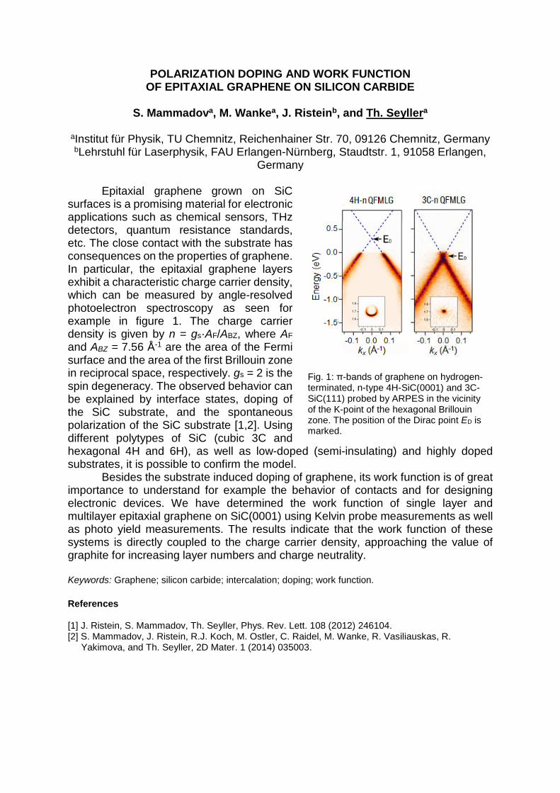
Epitaxial graphene grown on SiC surfaces is a promising material for electronic applications such as chemical sensors, THz detectors, quantum resistance standards, etc. The close contact with the substrate has consequences on the properties of graphene. In particular, the epitaxial graphene layers exhibit a characteristic charge carrier density, which can be measured by angle-resolved photoelectron spectroscopy as seen for example in figure 1. The charge carrier density is given by n = gs·AF/ABZ, where AF and ABZ = 7.56 Å-1 are the area of the Fermi surface and the area of the first Brillouin zone in reciprocal space, respectively. gs = 2 is the spin degeneracy. The observed behavior can be explained by interface states, doping of the SiC substrate, and the spontaneous polarization of the SiC substrate [1,2]. Using different polytypes of SiC (cubic 3C and hexagonal 4H and 6H), as well as low-doped (semi-insulating) and highly doped substrates, it is possible to confirm the model.
Besides the substrate induced doping of graphene, its work function is of great importance to understand for example the behavior of contacts and for designing electronic devices. We have determined the work function of single layer and multilayer epitaxial graphene on SiC(0001) using Kelvin probe measurements as well as photo yield measurements. The results indicate that the work function of these systems is directly coupled to the charge carrier density, approaching the value of graphite for increasing layer numbers and charge neutrality.
Keywords: Graphene; silicon carbide; intercalation; doping; work function.
References
[1] J. Ristein, S. Mammadov, Th. Seyller, Phys. Rev. Lett. 108 (2012) 246104.[2] S. Mammadov, J. Ristein, R.J. Koch, M. Ostler, C. Raidel, M. Wanke, R. Vasiliauskas, R.
Yakimova, and Th. Seyller, 2D Mater. 1 (2014) 035003.
Fig. 1: π-bands of graphene on hydrogen-terminated, n-type 4H-SiC(0001) and 3C-SiC(111) probed by ARPES in the vicinity of the K-point of the hexagonal Brillouin zone. The position of the Dirac point ED is marked.
A UNIVERSAL SUBSTRATE FOR THE STUDY OF TWO-DIMENSIONAL MATERIALS
Suhail Shah1, Raul D. Rodriguez1, Zoheb Khan1, Dhiraj Mehar1, Komal Vondkar1, Mahfujur Rahaman1, Evgeniya Sherement2, Michael Hietschold2, and
Dietrich R.T. Zahn1
1Semiconductor Physics, Technische Universität Chemnitz, D-09107 Chemnitz, Germany.
2Solid Surfaces Analysis Group, Technische Universität Chemnitz, 09107 Chemnitz, Germany
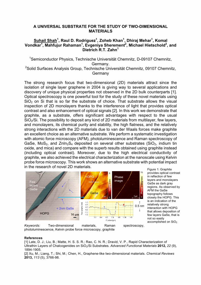
The strong research focus that two-dimensional (2D) materials attract since the isolation of single layer graphene in 2004 is giving way to several applications and discovery of unique physical properties not observed in the 2D bulk counterparts [1]. Optical spectroscopy is one powerful tool for the study of these novel materials using SiO2 on Si that is so far the substrate of choice. That substrate allows the visual inspection of 2D monolayers thanks to the interference of light that provides optical contrast and also enhancement of optical signals [2]. In this work we demonstrate that graphite, as a substrate, offers significant advantages with respect to the usual SiO2/Si. The possibility to deposit any kind of 2D materials from multilayer, few layers, and monolayers, its chemical purity and stability, the high flatness, and the relatively strong interactions with the 2D materials due to van der Waals forces make graphite an excellent choice as an alternative substrate. We perform a systematic investigation with atomic force microscopy (AFM), photoluminescence and Raman spectroscopy of GaSe, MoS2, and ZnIn2S4 deposited on several other substrates (SiO2, indium tin oxide, and mica) and compare with the superb results obtained using graphite instead (including optical contrast). Moreover, due to the high electrical conductivity of graphite, we also achieved the electrical characterization at the nanoscale using Kelvin probe force microscopy. This work shows an alternative substrate with potential impact in the research of novel 2D materials.
Keywords: Two-dimensional materials, Raman spectroscopy, photoluminescence, Kelvin probe force microscopy, graphite
References [1] Late, D. J.; Liu, B.; Matte, H. S. S. R.; Rao, C. N. R.; Dravid, V. P., Rapid Characterization ofUltrathin Layers of Chalcogenides on SiO2/Si Substrates. Advanced Functional Materials 2012, 22 (9),1894-1905.[2] Xu, M.; Liang, T.; Shi, M.; Chen, H., Graphene-like two-dimensional materials. Chemical Reviews2013, 113 (5), 3766-98.
Figure 1: Graphite provides optical contrast in reflection of few layers and monolayers GaSe as dark gray regions. As observed by AFM the GaSe topography follows closely the HOPG. This is an indication of the relatively strong interaction with HOPG that allows deposition of few layers GaSe, that is not so easily accomplished on SiO2
< 2nm GaSe
Few layers GaSe
HOPG
GaSe
Phase image
↑0.5 nm
↓HOPG
Hei
ght /
nm
0
8
Phas
e / d
egre
es
0
70
CONTROLLING OPTICAL ACTIVITY IN TW O -ATOM-THICK GRAPHENE
Cecilia Nogueza and A. Sánchez-Castillob aInstituto de Física, Universidad Nacional Autónoma de México, Apartado Postal 20-
364, Cd. México, 01000, México bEscuela Superior de Apan, Universidad Autónoma del Estado de Hidalgo, Chimalpa
Tlalayote, Municipio de Apan, Hidalgo, 43920, México Recently, the experimental realization of thin films with full control of the structural handedness down to the atomic scale was possible by stacking two graphene layers whose chiral properties are designed by an interlayer rotation angle [1]. The precise handedness can be controlled over several millimeters. This kind of uniform chiral metamaterial with two-atom-thick would provide a powerful tool for exploring and controlling chirality‐dependent phenomena, including circular dichroism, templated enantioselective growth in stereochemistry, electronic spin filters in spintronics, among other fields. In this work, we report theoretical results of the circular dichroism of a chiral stacking of two-dimensional materials are positioned layer-by-layer with precise control of the interlayer rotation. Using a time-perturbed first-principles theory [2], we show that these chiral properties originate from the large in-plane magnetic moment associated with the interlayer optical transition. Furthermore, we show that we can program the chiral properties of atomically thin films layer-by-layer graphene left-handed or right-handed films with structurally controlled CD spectra. The first‐principles calculation show that the multipole polarizability, an intrinsic and structure‐dependent quantity induced by the chiral nature of the interlayer optical transition, is the origin of the giant optical activity that is comparable to the highest known values for other materials.
Keywords: chiral graphene, 2D-materials, first-principles circular dichroism References [1] C.-J. Kim, A. Sanchez-Castillo, Z. Ziegler, Y. Ogawa, C. Noguez, J. Park, Nature Nanotechnology 11, (2016) 520–524. [2] F. Hidalgo, A. Sanchez-Castillo, C. Noguez, Physical Review B 79, (2009) 075438
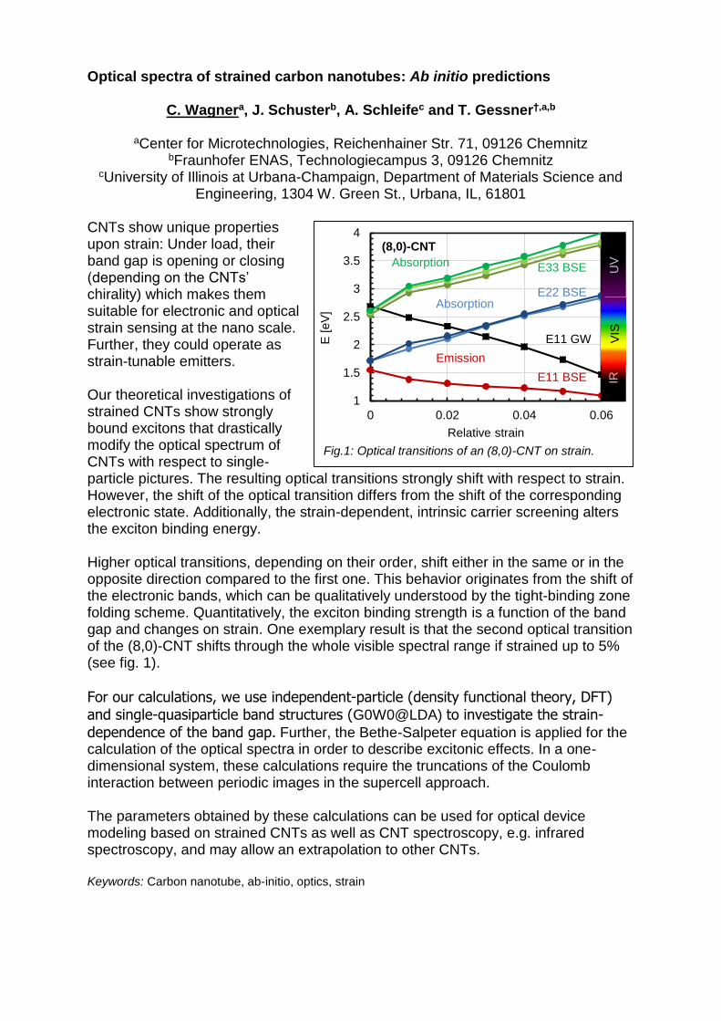
Fig.1: Optical transitions of an (8,0)-CNT on strain.
Optical spectra of strained carbon nanotubes: Ab initio predictions
C. Wagnera, J. Schusterb, A. Schleifec and T. Gessner†,a,b
aCenter for Microtechnologies, Reichenhainer Str. 71, 09126 Chemnitz bFraunhofer ENAS, Technologiecampus 3, 09126 Chemnitz
cUniversity of Illinois at Urbana-Champaign, Department of Materials Science and Engineering, 1304 W. Green St., Urbana, IL, 61801
CNTs show unique properties upon strain: Under load, their band gap is opening or closing (depending on the CNTs’ chirality) which makes them suitable for electronic and optical strain sensing at the nano scale. Further, they could operate as strain-tunable emitters.
Our theoretical investigations of strained CNTs show strongly bound excitons that drastically modify the optical spectrum of CNTs with respect to single-particle pictures. The resulting optical transitions strongly shift with respect to strain. However, the shift of the optical transition differs from the shift of the corresponding electronic state. Additionally, the strain-dependent, intrinsic carrier screening alters the exciton binding energy.
Higher optical transitions, depending on their order, shift either in the same or in the opposite direction compared to the first one. This behavior originates from the shift of the electronic bands, which can be qualitatively understood by the tight-binding zone folding scheme. Quantitatively, the exciton binding strength is a function of the band gap and changes on strain. One exemplary result is that the second optical transition of the (8,0)-CNT shifts through the whole visible spectral range if strained up to 5% (see fig. 1).
For our calculations, we use independent-particle (density functional theory, DFT) and single-quasiparticle band structures (G0W0@LDA) to investigate the strain-dependence of the band gap. Further, the Bethe-Salpeter equation is applied for the calculation of the optical spectra in order to describe excitonic effects. In a one-dimensional system, these calculations require the truncations of the Coulomb interaction between periodic images in the supercell approach.
The parameters obtained by these calculations can be used for optical device modeling based on strained CNTs as well as CNT spectroscopy, e.g. infrared spectroscopy, and may allow an extrapolation to other CNTs.
Keywords: Carbon nanotube, ab-initio, optics, strain
1
1.5
2
2.5
3
3.5
4
0 0.02 0.04 0.06
E [e
V]
Relative strain
(8,0)-CNT
E33 BSE Absorption
IR
VIS
U
V
Absorption E22 BSE
E11 GW
E11 BSE
Emission

DEFECTS IN TWO-DIMENSIONAL INORGANIC MATERIALS
Arkady V. Krasheninnikova,b
a Helmholtz Zentrum Dresden-Rossendorf, Institute of Ion Beam Physics and Materials Research, Germany
b Department of Applied Physics, Aalto University, Finland Following isolation of a single sheet of graphene, many other 2D systems such
as hexagonal BN sheets and transition metal dichalcogenides (TMD) were manufactured. Among them, TMD sheets have received particular attention, as these materials exhibit intriguing electronic and optical properties. Moreover, the properties can further be tuned by introduction of defects and impurities. In my talk, I will present the results [1] of our first-principles theoretical studies of defects (native and irradiation-induced) in graphene and inorganic 2D systems obtained in collaboration with several experimental groups. I will further discuss defect- and impurity-mediated engineering of the electronic structure of 2D materials. Keywords: 2D materials, defects, transmission electron microscopy, first-principles calculations References [1] Y.-C. Lin, et al., Nature Comm. 6 (2015) 6736; [2] Y.-C. Lin, et al., ACS Nano 9 (2015) 11249. [3] H.-P. Komsa, and A. V. Krasheninnikov, Phys. Rev. B 91 (2015) 125304. [4] O. Lehtinen et al., ACS Nano 9 (2015) 3274;
Line defects in inorganic 2D TMDs. (a) The grain structure, with the color coding corresponding to different grain orientations in MoSe2 [from Ref.4]. (b) A close-up view of a tilt grain boundary. c: A close-view of a mirror-twin-boundary within a grain. (d) The theoretical structure, as calculated using DFT. (e) A larger field of view image. Single vacancies are also visible. (f) Atomic structure of another type of mirror twin boundary structure (composed from 5-8 membered rings) observed in WSe2 [from Ref.1]. (g) Band structure and density of states of a mirror twin boundary in TMD.
Advances in Raman Spectroscopy of Graphene and Layered Materials
Andrea C. Ferrari Cambridge Graphene Centre, University of Cambridge, Cambridge, CB3 OFA, UK Raman spectroscopy is an integral part of graphene research [1]. It is used to determine the number and orientation of layers, the quality and types of edges, and the effects of perturbations, such as electric and magnetic fields, strain, doping, disorder and functional groups[2,3]. I will review the state of the art, future directions and open questions in Raman spectroscopy of graphene and related materials, focussing on the effect of disorder[3,4], doping[5,6] and deep UV laser excitation[7]. I will then consider the shear [8] and layer breathing modes(LBMs)[9], due to relative motions of the planes, either perpendicular or parallel to their normal. These modes are present in all layered materials[10,11]. Their detection allows one to directly probe the interlayer interactions [10,11]. They can also be used to determine the elastic constants associated with these displacements: the shear and out-of-plane elastic moduli[12]. This paves the way to the use of Raman spectroscopy to uncover the interface coupling of two-dimensional hybrids and heterostructures[10-12].
1. A. C. Ferrari et al. Phys. Rev. Lett. 97, 187401 (2006) 2. A.C. Ferrari, D.M. Basko, Nature Nano. 8, 235 (2013) 3. A.C. Ferrari, J Robertson, Phys. Rev. B 61, 14095 (2000) 4. G. Cancado et al. Nano Lett. 11, 3190 (2011) 5. M. Bruna et al. ACS Nano 8, 7432 (2014) 6. A. Das et al. Nat. Nanotechnol. 3, 210 (2008) 7. A.C. Ferrari, S. Milana, P. H. Tan, D. M. Basko, P. Venezuela, (2015) 8. P. H. Tan et al. Nature Materials 11, 294 (2012) 9. X. Zhang et al. Phys. Rev. B 87, 115413 (2013) 10. J. B. Wu et al. Nature Comms 5, 5309 (2014) 11. J.B. Wu et al. ACS Nano 9, 7440 (2015) 12. S. Milana et al. submitted (2016)

SURFACE-GRAFTED PARAMAGNETIC MACROCYCLIC COMPLEXES SEEN BY STM
C. Salazara, J. Lachb, F. Rückerla, D. Baumanna, S. Schimmela, M. Knupfera, B.Kerstingb, B. Büchnera,c,d, and C. Hessa,d
aLeibniz Institute for Solid State and Materials Research (IFW-Dresden), Helmholtzstrasse 20, 01171 Dresden, Germany
bInstitut für Anorganische Chemie, Universität Leipzig, 04103 Leipzig, Germany cInstitute for Solid State Physics, TU Dresden, 01069 Dresden, Germany
dCenter for Transport and Devices of Emergent Materials, TU Dresden, 01069 Dresden, Germany
The development of molecular nanostructures which contain magnetically bistable transition metal complexes arranged on planar surfaces is an active route towards materials with controllable magnetic or spintronic properties, leading to potential applications on information storage at the molecular level and molecular spintronics. Here we study the molecular anchoring and electronic properties of macrocyclic complexes fixed on gold surfaces [1]. Exchange-coupled macrocyclic complexes [Ni2L(Hmba)]+ were deposited ex-situ via 4-mercaptobenzoate ligands on the surface of a Au(111) single crystal from solution in dichloromethane. The combined results from STM and XPS show the formation of large monolayers anchored via Au-S bonds with a height of about 1.5 nm. Two apparent granular structures are visible: one related to the dinickel molecular complexes (cationic structures) and a second one related to the counter ions ClO4- which stabilize the monolayer. No type of short and long range order is observed. STM tip-interaction with the monolayer reveals higher degradation after eight hours of measurement. Spectroscopy measurements suggest a gap of about 2.5 eV between HOMO and LUMO of the cationic structures and smaller gap in the areas related to the anionic structures.
Paramagnetic Complexes: Self Assembled Monolayers; Scanning Tunneling Microscopy
References
[1] C. Salazar, J. Lach, F. Rückerl, D. Baumann, S. Schimmel, M. Knupfer, B. Kersting, B. Büchner,C. Hess, Langmuir 32 (2016) 4464.

TOWARDS UNDERSTANDING AND CONTROL OF ULTRATHIN ORDERED FILMS OF PHTHALOCYANINES AND PORPHYRINES
M. Hietschold, L. Smykalla
Solid Surfaces Analysis Group, Institute of Physics, Technische Universität Chemnitz, D-09107 Chemnitz, Germany
Two-dimensionally ordered ultrathin films (mostly monolayers) of various porphyrin and phthalocyanine derivatives on crystalline metallic substrates have been prepared by OMBE. Besides understanding of the self-assembled adsorbate structures observed using STM, also the electronic structure of the films has been studied by STS and PES. Controlled chemical modifications can be performed locally using the STM tip as well as globally using suitable thermal treatment. Specific examples to be discussed here are:
• Adsorption of metal-free tetra(p-hydroxyphenyl)porphyrin (H2THPP) onAu(111), Ag (111) and Ag(110) [1];
• STM tip-induced reversible deprotonation of single H2THPP molecules on Au(111) [2,3];
• Adsorption and heat-induced surface-polymerization of Cu-octobromotetra-phenylporphyrin (CuTTPBr8) on Au(111) [4];
• Self-metalation of metal-free phthalocyanine (H2Pc) on Ag(110) [5];• Charge transfer in PtPc-CoPc dimer layers.
An outlook will be given concerning future developments and applications.
Keywords: Ultrathin Organic Films; Adsorbate Structure; Surface Electronic Structure; Porphyrine Derivatives (H2THPP, CuTTPBr8); Phthalocyanine (H2Pc); Organic Molecular Beam Epitaxy (OMBE); Scanning Tunneling Microscopy (STM); Scanning Tunneling Spectroscopy (STS); Photoelectron Spectroscopy (PES); Surface Chemical Reaction; Polymerization; Self-Metalation.
References
[1] L.Smykalla, P.Shukrynau, C.Mende, T.Ruffer, H.Lang, M.Hietschold. Surf.Sci. 628 (2014), 132.[2] L.Smykalla, P.Shukrynau, C.Mende, T.Ruffer, H.Lang, M.Hietschold. Surf.Sci. 628 (2014), 92.[3] L.Smykalla, P.Shukrynau, C.Mende, H.Lang, M.Knupfer, M.Hietschold. Chem.Phys. 450 (2015),39.[4] L.Smykalla, P.Shukrynau, M.Korb, H.Lang, M.Hietschold. Nanoscale 7 (2015), 4234..[5] L.Smykalla, P.Shukrynau, D.R.T.Zahn, M.Hietschold. J.Phys.Chem. C 119 (2015), 17228.
GROWTH OF SELF-ASSEMBLED MONOLAYERS DIRECTLY ON FERROMAGNETIC METAL SURFACES
S. Tataya, M. Galbiatia, M. Matteraa, S. Delpratb, A. Forment-Aliagaa,E. Coronadoa, R. Mattanab, P. Seneorb
a Unidad de Investigación de Materiales Moleculares, Instituto de Ciencia Molecular, 46980 Paterna, Spain
b Unité Mixte de Physique CNRS/Thales associée à l’Université Paris-Sud, 91767 Palaiseau, France
Molecular spintronics combines the potential of chemistry with the spin degree of freedom provided by spintronics. In spintronic devices, metal/molecule hybridization can strongly influence interfacial spin properties going from spin polarization enhancement to its sign control [1]. SAMs are composed by a head, a body and an anchoring group that can be independently tuned, thus allowing an easy engineering of the spintronic barrier. In this scenario, while scarcely studied, self-assembled monolayers (SAMs) seem to be the perfect toy barriers to test these tailoring properties in molecular magnetic tunnel junctions (MTJs).
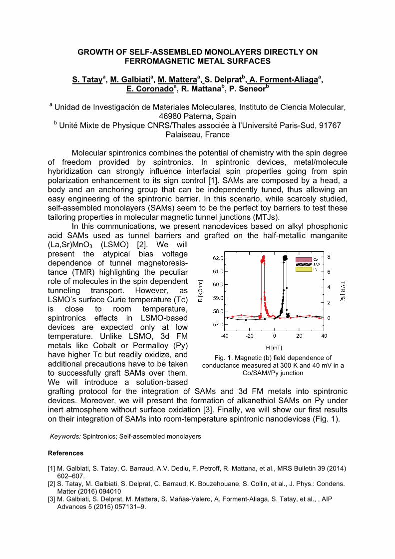
In this communications, we present nanodevices based on alkyl phosphonic acid SAMs used as tunnel barriers and grafted on the half-metallic manganite (La,Sr)MnO3 (LSMO) [2]. We will present the atypical bias voltage dependence of tunnel magnetoresis-tance (TMR) highlighting the peculiar role of molecules in the spin dependent tunneling transport. However, as LSMO’s surface Curie temperature (Tc) is close to room temperature, spintronics effects in LSMO-based devices are expected only at low temperature. Unlike LSMO, 3d FM metals like Cobalt or Permalloy (Py) have higher Tc but readily oxidize, and additional precautions have to be taken to successfully graft SAMs over them. We will introduce a solution-based grafting protocol for the integration of SAMs and 3d FM metals into spintronic devices. Moreover, we will present the formation of alkanethiol SAMs on Py under inert atmosphere without surface oxidation [3]. Finally, we will show our first results on their integration of SAMs into room-temperature spintronic nanodevices (Fig. 1).
Keywords: Spintronics;; Self-assembled monolayers
References
[1] M. Galbiati, S. Tatay, C. Barraud, A.V. Dediu, F. Petroff, R. Mattana, et al., MRS Bulletin 39 (2014)602–607.
[2] S. Tatay, M. Galbiati, S. Delprat, C. Barraud, K. Bouzehouane, S. Collin, et al., J. Phys.: Condens.Matter (2016) 094010
[3] M. Galbiati, S. Delprat, M. Mattera, S. Mañas-Valero, A. Forment-Aliaga, S. Tatay, et al., , AIPAdvances 5 (2015) 057131–9.
Fig. 1. Magnetic (b) field dependence of conductance measured at 300 K and 40 mV in a
Co/SAM//Py junction
NANOSCALE TRANSPORT STUDIES OF FUNCTIONAL ORGANIC SYSTEMS
P. F. Silesa,b, M. Devarajulua, F. Zhua,b, V. K. Bandaria, P. Robaschikc, G. Salvanc, D. R. T. Zahnc and O. G. Schmidta,b
aMaterial Systems for Nanoelectronics, Technische Universität Chemnitz, Germany bInstitute for Integrative Nanosciences, IFW- Dresden, Germany
cSemiconductor Physics, Technische Universität Chemnitz, Germany
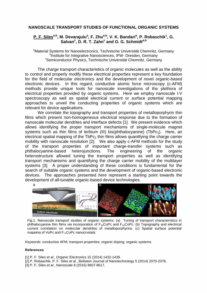
The charge transport characteristics of organic molecules as well as the ability to control and properly modify these electrical properties represent a key foundation for the field of molecular electronics and the development of novel organic-based electronic devices. In this regard, conductive atomic force microscopy (c-AFM) methods provide unique tools for nanoscale investigations of the plethora of electrical properties provided by organic systems. Here we employ nanoscale I-V spectroscopy as well as spatial electrical current or surface potential mapping approaches to unveil the conducting properties of organic systems which are relevant for device applications.
We correlate the topography and transport properties of metalloporphyrin thin films which present non-homogeneous electrical response due to the formation of nanoscale molecular dendrites and interface defects [1]. We present evidence which allows identifying the proper transport mechanisms of single-molecule magnet systems such as thin films of terbium (III) bis(phthalocyanine) (TbPc2). Here, an electrical spatial mapping of the TbPc2 thin films allows quantifying the charge carrier mobility with nanoscale resolution [2]. We also apply c-AFM methods for the study of the transport properties of important charge-transfer systems such as phthalocyanine-based heterojunctions. The engineering of the organic heterostructure allowed tuning the transport properties as well as identifying transport mechanisms and quantifying the charge carrier mobility of the multilayer systems [3]. A proper understanding of these conditions is fundamental for the search of suitable organic systems and the development of organic-based electronic devices. The approaches presented here represent a starting point towards the development of all-tunable organic-based device technologies.
Keywords: conductive AFM; transport properties; organic doping; organic systems
References
[1] P. F. Siles et al., Organic Electronics 15 (2014) 1432-1439.[2] P. Robaschik, P. F. Siles et al., Beilstein Journal of Nanotechnology 5 (2014) 2070-2078.[3] P. F. Siles et al., Nanoscale 8 (2016) 8607-8617.
Fig.1. Nanoscale transport studies of organic systems. (a) Tuning of transport characteristics in phthalocyanine thin films via incorporation of F16CuPc and F16CoPc. (b) Topography and electrical current correlation on molecular dendrites of metalloporphyrins. (c) Spatial surface potential mapping of VoPc and F16CuPc nanocrystals.
Charge transfer in Manganese-Phthalocyanine compounds
M. Knupfera, F. Rückerla, D. Waasa, T. Hahnb and J. Kortusb
aIFW Dresden, D-01171 Dresden, Germany bTU Bergakademie Freiberg, Leipziger Str. 23, D-09596 Freiberg, Germany
Manganese-Phthalocyanine (MnPc) harbors a number of interesting properties, which explains its importance for fundamental as well as more applied research activities. For instance, it is characterized by an unusual S = 3/2 spin state of the Mn2+ central ion, MnPc has even been referred to as a typical example of a molecular magnet. Moreover, it shows the smallest ionization potential amongst the transition metal phthalocyanines, and its optical absorption spectrum is far more complex as that of e.g. CuPc.
In this contribution, we will review investigations of charge transfer contributions to the optical absorption data, and the formation of new materials or interfaces based on MnPc, which are characterized by charge transfer reactions. In particular, it is demonstrated that the two energetically lowest absorption features or electronic excitations in bulk MnPc are due to charge transfer excitations, opposite to many other molecular solids where (Frenkel-type) intra-molacular excitations dominate. Further, the formation of MnPc/F16CoPc interfaces is discussed which are characterized by a spin and charge transfer at the interface. Finally, MnPc and the strong electron acceptor F4TCNQ form a charge transfer (bulk) material in which the MnPc molecules are fully ionized.
This work has been supported by the Deutsche Forschungsgemeinschaft within the Research Unit FOR 1154.
Keywords: Manganese Phthalocyanine, Charge transfer excitations and reactions, Electron Spectroscopy
(MAGNETO-)OPTICAL PROPERTIES OF MAGNETIC MOLECULAR LAYERS
G. Salvana, M. Fronka, P. Robaschika,b, F. Lungwitza,c, T. Rüfferd, C. Mended, H.Langd, T. Hahne, J. Kortuse, D. R. T. Zahna
aSemiconductor Physics, Institute of Physics, Technische Universität Chemnitz, 09126 Chemnitz, Germany bpresent address: Department of Materials and London Centre for Nanotechnology, Imperial College London, London SW7 2AZ, UK cpresent address: Scaling Phenomena Division, Helmholtz-Zentrum Dresden-Rossendorf, 01328 Dresden, Germany dInorganic Chemistry, Institute of Chemistry, Technische Universität Chemnitz, 09126 Chemnitz, Germany eInstitute of Theoretical Physics, TU Bergakademie Freiberg, 09596 Freiberg, Germany
In this contribution we will provide an overview on investigations of the magneto-optical response of thin films of phthalocyanine molecules on substrates which are relevant for (spin) organic field effect transistors (SiO2) or vertical spin valves (Co) in order to explore the possibility of implementing phthalocyanines in magneto-electronic devices, the functionality of which includes optical reading.
The optical and magneto-optical properties of phthalocyanine thin films prepared by organic molecular beam depositio [1,2,3] or by spin coating [4] on silicon substrates were investigated by variable angle spectroscopic ellipsometry (VASE) and magneto-optical Kerr effect (MOKE) spectroscopy at room temperature. The magneto-optical activity of phthalocyanine molecules in the UV-vis spectral range is determined by the highest occupied and lowest unoccupied molecular orbitals and their hybridization degree with the central metal ion. In addition to the details of the molecular electronic structure, the growth mode and hence the molecular orientation with respect to the substrate can dramatically tune the magneto-optical activity. In the case of phthalocyanine films, the tuning of the molecular orientation can be achieved by controlling the substrate surface properties via the substrate treatment [1] or via exploiting a templating effect introduced by ultra-thin molecular layers or byusing metallic ferromagnetic substrates (Co).Our observations open new perspectives for combining magnetism and optics indevices such as spin-OFETs and organic spin valves. The change in polarizationstate of a linearly polarized light beam reflected by an active layer of TbPc2 might beused as a diagnosis tool for eventual electronic changes under appliedelectric/magnetic field in a spintronic device.
Keywords: phthalocyanines; porphyrins; magneto-optical response
References
[1] M. Fronk, B. Bräuer, J. Kortus, O.G. Schmidt, D.R.T. Zahn, G. Salvan Phys. Rev. B 79 (2009),235305.
[2] B. Bräuer, M. Fronk, D. Lehmann, D. R. T. Zahn, G. Salvan, J. Phys. Chem. B 113 (2009) 14957.[3] P. Robaschik, M. Fronk, M. Toader, S. Klyatskaya, F. Ganss, P.F. Siles, O.G. Schmidt, M.
Albrecht, M. Hietschold, M. Ruben, D.R.T. Zahn, G. Salvan, J. Mat. Chem. C 3 (2015) 8039.[4] T. Birnbaum, T. Hahn, C. Martin, J. Kortus, M. Fronk, F. Lungwitz, D. RT Zahn, G. Salvan, J.
Phys.: Cond. Mat. 26 (2014) 104201.

Modulating light emission in a spin-OLED through spin injection at high voltages
H. Prima-García,a J.P. Prieto-Ruiz,a S.Gómez-Miralles,a A. Riminucci,b P.Graziossib, V. A. Dediu,b E. Coronado, *a
aInstituto de Ciencia Molecular (ICMol), Universidad de Valencia.
b Instituto per lo Studio dei Materiali Nanostrutturati ISMN - CNR, Via Gobetti, 101,
Bologna, 40129, Italy
Spin-based electronics is one of the emerging branches in today’s nanotechnology and the most active area within nanomagnetism. So far spintronics has been based on conventional materials like inorganic metals and semiconductors. Still, an appealing possibility is that of using molecule-based materials, as components of new spintronic systems [1]. In particular, by taking advantage of a hybrid approach one can integrate molecular materials showing multifunctional properties into spintronic devices. In this talk we illustrate the use of this approach to fabricate multifunctional molecular devices combining light and spin-valve properties (i.e., Spin-OLEDs). So far only one report has been published which is based on the fabrication of an organic light emitting diode (OLED) with ferromagnetic electrodes [2]. Our approach is based on the use of a HyLED (Hybrid Light Emitting Diode) structure in which LSMO and Co are used as ferromagnetic electrode. This device works simultaneously as a spin valve and an electroluminescent device at low temperatures [3]. This new approach leads to a robust organic luminescent device in which light emission can be enhanced and modulated upon application of an external magnetic field (Figure 1)
Molecular Spintronic, Spin-OLEDs, multifunctional devices
References
[1] J. Camarero, E. Coronado, J. Mater. Chem. 19, 1678 (2009).
[2] T. Nguyen, E. Ehrenfreud, Z. Valy Vardeny, Science 337, 204 (2012).
[3] Opto-spintronic device and its fabrication method.E. Coronado Miralles; H. Prima Garcia,
J.P. Prieto Ruiz. Spanish National Patent. Ref. 201300083, 2013, University of Valencia.
Figure 1. Magnetoresistance at 9 V and 20K of
the PEIE SO. Black arrows depict the field
sweep direction. Purple and grey arrows point
the FM electrodes magnetization direction.
Fig. 1. Venue of ICSFS 18

ORGANIC NANOSTRUCTURE DEVICES BASED ON ROLLED-UP NANOMEMBRANES
F. Zhua,b P. F. Silesa,b, V. K. Bandaria,b, and O. G. Schmidta,b
a Faculty of Electrical Engineering and Information Technology, Technische Universität Chemnitz, Reichenhainer Straße 70, 09126 Chemnitz, Germany
b Institute for Integrative Nanosciences, IFW Dresden, Helmholtz Straße 20, 01069 Dresden, Germany
Over the past decades organic nanostructures have attracted huge interest due to their importance in understanding fundamental properties and creating molecular electronic/spintronic nanodevices [1, 2]. Normally, molecular nanodevices rely on electronically connecting molecules through the formation of metallic electrodes. However, the fragile nature of molecules make it difficult to realize nondestructive metal/organic contacts when the metal electrode layers are fabricated by conventional methods of metal deposition, thereof the development of molecular nanodevices has been severely restricted. In this talk we will summarize the contribution from our project team towards the objectives of the TMS research group. A novel robust contact method based on strained and rolled-up nanomembranes will be introduced after shortly reviewing the state-of-art ‘soft’ contact techniques for molecular devices [3]. The fabrication of self-assembled-monolayer (SAM) diodes and spin-valves structures consisting of non-destructive (ferromagnetic) metal/organic interfaces will be demonstrated. Furthermore, the local investigation via atomic force microscope (AFM) techniques and the application of organic nanocrystal diodes for sensing NO2 will be discussed [4, 5].
Keywords: Nanomembrane, Rolled-up technology, Organic nanostructure, Organic spin valves
References
[1] M. Ratner, Nat Nano, 2013, 8, 378.[2] D. Xiang, et al., Chem. Rev., 2016, 116, 4318.[3] C. C. Bof Bufon, et al., Nano Lett., 2011, 11, 3727.[4] P. F. Siles, et al, Nanoscale, 2016, 8, 8607.[5] A. R. Jalil, et al., Adv. Mater., 2016, 28, 2971.