design and characterization of a superconducting …ferdinand_diplomarbeit_2014.pdfwmi design and...
TRANSCRIPT

WMI
Design and characterization
of a superconducting beam-splitter
for quantum information processing
Diploma Thesis
Ferdinand Loacker
December 2013
Supervisor: Prof. Dr. Rudolf Gross
Technische Universitat Munchen

Foremost, I want to dedicate this thesis to my wonderful family. They supported me
throughout my whole life, and I know it wasn’t always easy. It is also in memory of
my grandfather, whose absence lies like a shadow on everyday life.

Erklarung / Declaration of Originality
Mit der Abgabe der Diplomarbeit versichere ich, dass ich die Arbeit selbstandig
verfasst und keine anderen als die angegebenen Quellen und Hilfsmittel benutzt
habe.
By submission of this thesis I hereby certify, that this diploma thesis is my own work
and no sources other than the ones given have been used.
Garching, 18. Dezember 2013
Ort, Datum Ferdinand Loacker


Contents
Erklarung / Declaration of Originality i
Contents iii
1 Introduction 1
2 Microwave fundamentals 5
2.1 Coplanar waveguides . . . . . . . . . . . . . . . . . . . . . . . . . . . 5
2.2 Scattering parameters . . . . . . . . . . . . . . . . . . . . . . . . . . 11
2.3 The quadrature (90) hybrid . . . . . . . . . . . . . . . . . . . . . . . 12
3 Experimental techniques 19
3.1 Measurement setup and equipment . . . . . . . . . . . . . . . . . . . 19
3.2 Sample package . . . . . . . . . . . . . . . . . . . . . . . . . . . . . . 22
3.2.1 Sample Chip and PCB . . . . . . . . . . . . . . . . . . . . . . 22
3.2.2 Packaging . . . . . . . . . . . . . . . . . . . . . . . . . . . . . 24
3.3 Time Domain Reflectometry . . . . . . . . . . . . . . . . . . . . . . . 27
4 Experimental results 33
4.1 Characterization and optimization of the sample package . . . . . . . 33
4.1.1 Analysis of press-connector sample holder . . . . . . . . . . . 33
4.1.2 Matching between PCB and SMA press-contact connector . . 37
4.1.3 Design parameters and performance of PCBs with surface-
mount mini-SMP connectors . . . . . . . . . . . . . . . . . . . 44
4.1.4 Comparison between press-contact and surface-mount connec-
tor sample holder . . . . . . . . . . . . . . . . . . . . . . . . . 49
4.1.5 Analysis of PCB/chip connection with surface-mount sample
holder using mini-SMP connectors . . . . . . . . . . . . . . . . 53
4.2 The 90 hybrid ring . . . . . . . . . . . . . . . . . . . . . . . . . . . . 67
5 Summary & Outlook 73
A Chip fabrication 75
iii

iv CONTENTS
B Resist layer thickness 81
C Internal cryostat cables 85
D Box top metal covers and air modes 89
Bibliography 91

Chapter1Introduction
Quantum computation has the potential to perform certain computational tasks so
efficient, that modern super computers perform like pocket calculators in compari-
son. However, this does not mean that they are suited for every possible task. The
performance is only superior for certain applications, including factorization and de-
cryption. In the context of fundamental research, quantum computers are believed
to be relevant because of their ability to efficiently simulate complex quantum sys-
tems. This idea was originally sugessted by Richard Feynman in 1982 [1] and David
Deutsch showed in 1985 that theoretically any physical process could be simulated
this way [2].
For a regular computer that relies solely on the two possible states of a classical
bit, 0 and 1, computation time increases exponentially with the size of the prob-
lems mentioned above. In contrast, a quantum algorithm reduced this scaling to
a polynomial law by making explicit use of quantum mechanics on the level of the
underlying logic1. A visual depiction of a quantum bit (qubit) is conveniently ob-
tained by the Bloch sphere representation, where all possible superposition states
of a quantum two-level system with the basis states |0〉 and |1〉 are located on the
surface of the sphere. As we can see in Fig. 1.1, the qubit state |Ψ〉 is then repre-
sented by the Bloch angles θ (amplitude) and φ (phase). In combination with the
quantum property of entanglement, this (with respect to the two states of a classical
bit) greatly extended computational space forms the basis of the potential speedup
achievable by quantum algorithms.
One specific implementation possibility is described in the following: circuit quan-
tum electrodynamics (cQED) [4]) was suggested by Blais in 2004 [5] and first ex-
perimentally verified soon after that [4, 6]. In cQED, qubits are coupled to (quasi)
one-dimensional microwave resonators (CPW structures) with superconducting ma-
terials in order to minimize environment-induced losses. These structures are macro-
scoping in size, since the typical frequency of operation is in the order of several gi-
1Whereas for the computation of a quantum mechanical system with n two-level systems nn
classical bits are necessary, a quantum computer only requires the employement of n qubits.
1

2
Figure 1.1: Bloch sphere representation of a qubit taken from Ref. [3] (with
the two states ground |g〉 ≡ |0〉 and excited |e〉 ≡ |1〉).
gahertz, corresponding to several mm long resonators2. The superconducting qubits
are Josephson-junction-based circuits [7] and act as ‘artificial atoms’ (matter) via
the resonator, this quantum matter can interact with microwave light (photons).
The information of the system can now be shared or transferred between qubit and
photon, which can leak out of the resonator. Such a propagating photon itself can
act as an information carrier, an approach that was formerly exclusive to quantum
optics [8].
The utilization of microwave photons for quantum information processing includes
several benefits. They have good coherence properties in superconducting waveguide
structures and are naturally bound to distribute quantum information. Furthermore,
superconducting circuits can mediate strong interactions between them which should
allow for deterministic gates. Consequently, the young field of propagating quantum
microwaves is gaining increasing popularity for quantum computation and quantum
simulation.
The ability to combine and split propagating waves is a necessity for these tasks and
can be achieved through passive components such as the quadrature hybrid which
acts as a beam splitter for the microwave photons [9]. It features a scalable port
configuration in the sense that a planar interferometer can be constructed from two
adjacent hybrids on a single chip without crossing microwave lines.
In this work, this fundamental linear element (the quadrature 90 hybrid) is mea-
sured and its properties are examined. In addition, the sample package enclosing
the device is analyzed and optimized.
2The typical energy gap of a qubit is 5 GHz and the hybrid-ring has to be designed/matched
accordingly.

1 Introduction 3
The thesis is structured as follows: Chapter 2 gives insight into the relevant mi-
crowave theory. In Ch. 3, an overview of sample package and measurement setup
are presented. Chapter 4 is divided in two parts. In the first section, critical con-
nections between the various components of the sample package are examined and
optimized, while the second part employs the achieved accomplishments in an anal-
ysis of the beam splitter. In Ch. 5, the results (of this thesis) are summarized and
an outlook on the future development is given.

4

Chapter2Microwave fundamentals
This chapter presents the theoretical foundations relevant for the design of microwave
circuits and devices. First, the geometry of coplanar waveguide transmission lines
(CPW) is presented in Sec. 2.1. The scattering parameters are introduced in Sec. 2.2.
One possible application, the quadrature (90) hybrid examined during this thesis,
is discussed in Sec. 2.3.
2.1 Coplanar waveguides
A coplanar waveguide is a patricular type of a planar microwave transmission line.
It commonly consists of a center strip conductor amidst two ground planes ontop
a dielectric substrate. It was originally developed by C. P. Wen in 1969 [10]. One
advantage of CPWs is their design flexibilty, allowing for a significant amount of
freedom in the choice of the widths of both center conductor and the gaps to the
ground plane. As we will see later, typically only the ratio of these two quantities
is fixed. Application in classical microwave engineering range from amplifiers and
printed antennas to switches [11].
In this section, the main characteristics of CPWs are discussed and their derivation
is presented following Ref. [11, 12]. First, the double-layer CPW is analyzed. This is
an extended version of the original design, capable of characterizing a sample with
two different substrates of finite thickness. Figure 2.1 shows the schematic composi-
tion of such a CPW structure with metal covers, a top substrate layer with thickness
h2 and dielectric constant εr2 and a second one at the bottom with hight h1−h2 and
dielectric constant εr1. The distances to the metal covers are h3 or h4 respectively
and thickness of the textured metal layer is t. This general approach allows for
analyzing a chip placed in a PCB, a setup that is used for several experiments in
this thesis, by considering the dielectric constants of both components. In addition,
the PCB can be examined by itself with the appropriate parameters, setting εr1 = 1
and therefore eliminating the partial capacitance C2 presented in Fig. 2.2 and only
calculating a CPW on a single substrate.
The charactersitic parameters of a CPW are the effective dielectric constant εeff and
5

6 2.1 Coplanar waveguides
ε
ε
t
h
h
h
4
3
1
h2
0
0ε
εr1
r2
ε0
ε0
wgg
Figure 2.1: Schematic of CPW on double-layer dielectric substrate; adapted
version from Ref. [11].
the characterstic impedance Z0. They are determined through conductor properties
such as its dimensions (width w, gap g and thickness t) and the dielectric substrates
(thickness hi with dielectric ε0εri). For this analysis, the conductor is assumed to be
lossless. For superconducting materials [13] (perfect conductivity), this assumption
should be appropriate and copper is an excellent conductor as well. At this point,
the ground planes are of infinite width and the substrate is considered isotropic. A
quasi-static approach is utilized to determine the potential in order to calculate the
capacitances (using conformal mapping techniques). Usually, the determination is
conducted with a full-wave analysis, a complicated process that requires excessive
amounts of computing capacity (and time) [14] because of the retarded potential.
One possible solution is the employement of analytic formulas in a quasi-static ap-
proximation, a technique that achieves good results [15]. According to Ref. [16], one
aspect of the quasi-static approximation is that the propagation mode in the trans-
mission lines is a pure transverse electromagnetic modes (TEM). This circumstance
concerns the relation of wavelength (λ) and structure dimensions (d) such as w and
g. If d is diminutive in comparison to λ, usually fulfilled for frequencies below 10 GHz
and the utilized chip designs in particular, the longitudinal field components are sig-
nificantly smaller than transversal ones. The main principle of this approximation
is that for high velocities the change of the self-induced influenced of the retarded
potential is slow compared to the velocity (the system is in an equilibrium).
To analyze the CPW from Fig. 2.1, it is first devided into several parts that are
examined seperately as seen in Fig. 2.2. The electric fields are assumed to be only
in the appropriate region.
CCPW = Cair + C1 + C2. (2.1)
Following the Veyers-Fouad Hanna approximation [15], the total capacitance of the
CPW (CCPW) is a superposition of the partial capacitances of these regions.
Cair is examined first, giving the capacitance between the plane containing center
strip conductor and ground planes and the top and/or bottom metal covers.

2 Microwave fundamentals 7
t
h
hh =
4
3 1
ε = 1r
ε = 1r
wgg
t
h1
ε - 1r1
ggw
a)
b)
th
2ε -r2
ggwc)
ε r1
Figure 2.2: Schematic for partial capacitances: a) Cair, b) C1, c) C2.
Adjusted illustration taken from Ref. [11].
The space between these layers is filled with air (εr = 1). It is defined as:
Cair = 2ε0K(k3)
K(k′3)+ 2ε0
K(k4)
K(k′4), (2.2)
where K is the complete elliptical integral of the first kind. The arguments k and k’
are dependent on the geometry:
ki =
tanh
(πw
4hi
)tanh
(π(w + 2g)
4hi
) (2.3)
k′i =√
1− ki2, i = 3 or 4 (2.4)
The top metal cover represents the box where the PCB is placed, while the layer
at the bottom in our case refers to to the conductor backed coplanar waveguide
(CBCPW). The CBCPW is presented later in this section since some adjustements
have to be considered. According to Ref. [17], an approximation for the complete
eliptic integrals can be given for arbitrary ki.
If 0 < k ≤ 1/√
2, the approximation takes the following form with m = k2:
K(k)
K(k′)= −π
[ln
(m
16+ 8
(m16
)2
+ 84(m
16
)3
+ ...
)]−1
, (2.5)

8 2.1 Coplanar waveguides
while for 1/√
2 ≤ k < 1, this equation is utilized with m1 = 1− k2 :
K(k)
K(k′)= − 1
π
[ln
(m1
16+ 8
(m1
16
)2
+ 84(m1
16
)3
+ ...
)]. (2.6)
The expressions for the other (partial) capacitances as depicted in Fig. 2.2 are:
C1 = 2ε0(εr1 − 1)K(k1)
K(k′1), (2.7)
with
k1 =
sinh
(πw
4h1
)sinh
(π(w + 2g)
4h1
) , (2.8)
k′1 =√
1− k12. (2.9)
For C2, the equation is as follows:
C2 = 2ε0(εr2 − εr1)K(k2)
K(k′2), (2.10)
with
k2 =
sinh
(πw
4h2
)sinh
(π(w + 2g)
4h2
) (2.11)
and
k′2 =√
1− k12. (2.12)
Substituting the Eqs. (2.2), (2.7) and (2.10) into Eq. (2.1) gives for the capacitance
CCPW:
CCPW = 2ε0
[(K(k3)
K(k′3)+K(k4)
K(k′4)
)+ (εr1 − 1)
K(k1)
K(k′1)+ (εr2 − εr1)
K(k2)
K(k′2)
]. (2.13)
An expression for εeff under quasi-static approximation is:
εeff =CCPW
Cair
. (2.14)
With the equations for Cair (2.2) and CCPW (2.13), εeff can be converted to:
εeff = 1 + q1(εr1 − 1) + q2(εr2 − εr1). (2.15)
where the partial filling factors q1 and q2 are defined as follows:
q1 ≡K(k1)
K(k′1)
2ε0Cair
, (2.16)
q2 ≡K(k2)
K(k′2)
2ε0Cair
. (2.17)

2 Microwave fundamentals 9
ε ε
t
h
h4
r0
Figure 2.3: Schematic for CBCPW with top metal cover on a dielectric
substrate taken from Ref. [11].
This leads to the expression for the characteristic impedance Z0:
Z0 =1
CCPWvph
=1
cCair√εeff
, (2.18)
using
vph =c√εeff
(2.19)
with the velocity of light in free space c.
The PCB used in this thesis has a particular design, namely a CBCPW. How-
ever, identifying the conductive layer at the bottom with the real ground plane of a
CBCPW is not entirely correct. In the following discussion, the differences are em-
phasized. For a first overview, only one dielectric (εr) of thickness h is considered.
Figure 2.3 illustrates the appropriate schematic. The distance to the top metal cover
remains h4.
The effective dielectric constant εeff now fulfills the following equation:
εeff = 1 + q(εr − 1), (2.20)
where
q =
K(k3)
K(k′3)
K(k3)
K(k′3)+K(k4)
K(k′4)
(2.21)
ki =
tanh
(πw
4hi
)tanh
(π(w + 2g)
4hi
) , with hi = h for k3 and hi = h4 for k4, (2.22)
k′i =√
1− ki2, i = 3 or 4. (2.23)
This expression for εeff resembles Eq. (2.15) when εr2 = 1 (and for h2 = 0), thus h
equals h1 and εr = εr1. Although, the filling factor q has changed. Comparing q to

10 2.1 Coplanar waveguides
q2 [Eq. (2.16)] for h = h1 = h3 exemplifies the difference:
q
q1
=
sech
(πw
4hi
)sech
(π(w + 2g)
4hi
) (2.24)
using the expression for the hyperbolic secant
1
cosh(x)= sech(x). (2.25)
Considering a second substrate C2 [Eq. (2.10)], it is again assumed that the electric
field is only present in the appropriate regions (see Fig. 2.2). Therefore, C1 is
unaffected as in Eq. (2.7) and C2 remains identical to Eq. (2.10). Hence εeff for a
double-layer CBCPW is given by:
εeff = 1 + q(εr − 1) + q2(εr2 − εr1), (2.26)
with the partial filling factors q from Eq. (2.21) and q2 given by Eq. (2.17).
The finite dimensions of the ground plane must also be considered, especially in
the case of PCB and chip. First, the partial capacitance concept is extended for Cair
[Eq. (2.2)] by adding the new region C0, giving the capacitance between center strip
conductor and ground planes in their layer of thickness t:
C0 = 4ε0K(k)
K(k′)(2.27)
with
k =c
b
√b2 − a2
c2 − a2, (2.28)
where a = w/2, b = a + g and c = (w/2) + g + d with d being the width of the
ground planes.
Then, the expressions for the other k, ki has to be adjusted as follows:
ki =
tanh
(πc
2hi
)tanh
(πb
2hi
)√√√√√√√
tanh2
(πb
2hi
)− tanh2
(πa
2hi
)tanh2
(πc
2hi
)− tanh2
(πa
2hi
) (2.29)
with substituting sinh for tanh in the case of C2. The expression for k′ and every k′iis allways given by:
k′ =√
1− k2 (2.30)
With these last equations, every component of the real sample package (Sec. 3.2)
is covered by our discussion: The possible presence or absence of a chip in form
of a double-layer CPW, the immediate conductor backing of a CBCPW and the

2 Microwave fundamentals 11
Z Z
S21
S12
1 211 22
a1
b1
a2
b2
S S
port port
Figure 2.4: Illustration from Ref. [18] of a two port model, denominating
and explaining the appropirate S-parameters. The reflection at a port is
also denoted as Γ, for example at port 1 with S11 = Γ.
finite dimensions of the of ground planes (FWCPW). With the presented equations
it is possible to determine the design parameters for width and gap to match a
characteristic impedance of generally 50 Ω, a standard value of microwave equipment.
Width and gap are very adjustable and for a fixed value for one of these parameters,
the other one can be calculated for a given characteristic impedance.
2.2 Scattering parameters
In this section, the scattering parameters (or S-parameters) are explained assuming
a lossless network. An illustration to designate them is shown in Fig. 2.4. For a
two-port device, the S-parameters are definded as described in Ref. [18] and their
expression is in accordance with the general approach for a N -port network presented
in Ref [12]: (b1
b2
)=
(S11 S12
S21 S22
)(a1
a2
)(2.31)
The independent variables ai (i = 1, 2 denotes the port) are normalized incident
voltages (V +i )and the dependent factors bi the normalized reflected voltages (V −i ).
At first, port 1 is excited with no incident wave at port 2, thus setting a2 = 0. Under
the assumptions of a termination of matched characteristic impedance Z at port 2
and a lossless network, no power is lost. Therefore, the input reflection coefficient
S11 can be calculated according to Eq. (2.31):
S11 =V −1V +
1
, (2.32)
The forward voltage gain S21 (or transmission from port 1 to port 2) is given by:
S21 =V −2V +
1
, (2.33)
Similarly, for an incident wave at port 2 with the appropriate setup one gets:
S22 =V −2V +
2
, (2.34)

12 2.3 The quadrature (90) hybrid
and
S12 =V −1V +
2
. (2.35)
S-parameters are usually given in decibel (dB):
Sij[dB] = −20 log10 |Sij|. (2.36)
With the quadrature value of a scattering parameter |Sij|2, the relation for power is
given instead of voltages.
2.3 The quadrature (90) hybrid
In this section, the standard quadrature hybrid, also known as 90 hybrid ring or
branch-line hybrid/coupler, is discussed following Ref. [11, 12]. The device acts as a
3 dB beam splitter. When a signal is incident on port 1 (2,3,4), it is divided equally
(3 dB) into the “direct” port 2 (1,4,3) and the “coupled” port 3 (4,1,2). The remain-
ing port 4 (3,2,1) is isolated, i.e., there is no outgoing voltage. First, an overview of
the general design and the important parameters is prestend. Then the scattering
matrix of the device is calculated using even-odd-mode analysis. The hybrid ring
is assumed to be lossless and an illustration of the actual layout can be found in
Sec. 4.2.
An equivalent circuit model of the quadrature hybrid is shown in Fig. 2.5. This
illustration also contains important design information concerning the four sections
of the hybrid, the two through lines and the two branch lines.
Since the structure is very symmetric, S can be simplified as shown in Eq. (2.37).
For an ideal device, the entire matrix can be expressed in terms of the S-parameters
Si1:
S =
S11 S12 S13 S14
S21 S22 S23 S24
S31 S32 S33 S34
S41 S42 S43 S44
=
S11 S21 S31 S41
S21 S11 S41 S31
S31 S41 S11 S21
S41 S31 S21 S11
(2.37)
To determine the entries of the first column (Si1 with i = 1, 2, 3, 4), the symmetry
of the hybrid ring is utilized, allowing for an even-odd-mode analysis1. It describes
the propagation of an electromagnetic wave along a CPW as the superposition of
the two normal modes responses even and odd. For the case of the hybrid ring, an
input of intensity I applied at port 1 is therefore devided into two equal ones (+I/2)
at the ports 1 and 4 for the even mode and +I/2 at port 1 and −I/2 at port 4
for the odd mode. When combined, the superposition results in a total input at
port 1 of I and 0 at port 4 as intended. Figure 2.6 illustrates this excitation. The
1Usually, this method is employed for CPWs which are in close proximity so that their electro-
magnetic fields can interact, observed through power coupling in between them.

2 Microwave fundamentals 13
Z0
Z0
Z0
Z0
Z /√20
Z0 Z0λ/4
λ/4
Z /√20
λ/4
λ/4
Port 1
Input
Port 4
Isolated
Port 2
Direct
Port 3
Coupled
T-junction
through-line
branch-line
Figure 2.5: Illustration of equivalent circuit model of the quadrature hybrid,
taken from Ref. [11]. Z0 is the characteristic impedance of the input and
output lines and λ refers to the working frequency of the device. λ/4 also
determines the physical dimensions of the hybrid ring.
advantage of this technique is that through the symmetric application of sources,
the already symmetric structure of the hybrid ring can be divided into two identical
sub-circuits at the symmetrical plane while the information of the excluded section
remains in the form of the boundary condition that is determined through the type
of termination (for example an open termination for the even mode) [19]. Therefore,
it is sufficient to analyse one sub-circuit while retaining all the relevant information.
The actual branch-line hybrid presented in Fig. 2.5 is first divided into two identical
halves, utilizing the symmetry of the structure as seen in Fig. 2.7. The excitation
of one port (or input voltage V) is divided in even (or symmetric) and odd (anti-
symmetric) excitations. For the even mode, there is the voltage volt at both sides of
the symmetry axis, a so-called magnetic wall, and an electric wall in the case of the
odd mode where the voltages have an identical amplitude |V| but show a switched
sign. Splitting the circuit along this axis is equivalent to an open termination (even-
mode) or short termination (odd-mode) respectively. Additional splitting (along
the symmetry axis) of the remaining circuit further reduces the structure that can
in turn be excited with an even- and odd-mode as shown in Fig. 2.8. This simplifies
the calculation while retaining a complete description of the quadrature hybrid. In
conclusion, there is only one port left with 4 modes that can be analyzed seperately
while preserving circuit symmetry: the T-junction. The planes of symmetry become
virtual short or open terminations respectively. Using superposition, the final result
is a coherent summation of these results following Ref. [20].
14 2.3 The quadrature (90) hybrid
I /√2
λ/4λ/4
λ/4
λ/λ/41 2
4 3
I+ /2
I+ /2
I /√2
I
I
I
I
I I
I /√2
λ/4λ/4
λ/4
λ/λ/41 2
4 3
I+ /2
I- /2
I /√2
I
I
I
I
I I
I /√2
λ/4λ/4
λ/4
λ/λ/41 2
4 3
I+
0
I /√2
I
I
I
I
I I
even
odd
S11 S21
S41 S31
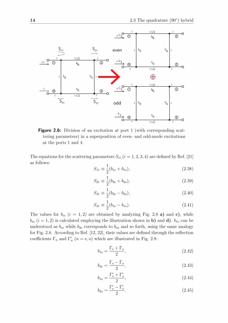
Figure 2.6: Division of an excitation at port 1 (with corresponding scat-
tering parameters) in a superposition of even- and odd-mode excitations
at the ports 1 and 4.
The equations for the scattering parameters Si1 (i = 1, 2, 3, 4) are defined by Ref. [21]
as follows:
S11 ≡1
2(b1e + b1o), (2.38)
S21 ≡1
2(b2e + b2o), (2.39)
S31 ≡1
2(b2e − b2o), (2.40)
S41 ≡1
2(b1e − b1o). (2.41)
The values for bie (i = 1, 2) are obtained by analyzing Fig. 2.8 a) and c), while
bio (i = 1, 2) is calculated employing the illustration shown in b) and d). b1e can be
understood as bee while b2e corresponds to boe and so forth, using the same analogy
for Fig. 2.8. According to Ref. [12, 22], their values are defined through the reflection
coefficients Γn and Γ′n (n = e, o) which are illustrated in Fig. 2.8:
b1e =Γe + Γo
2, (2.42)
b2e =Γe − Γo
2, (2.43)
b1o =Γ′e + Γ′o
2, (2.44)
b2o =Γ′e − Γ′o
2. (2.45)

2 Microwave fundamentals 15
I /√2
λ/8λ/8
λ/4
λ/λ/4
λ/4
λ/4
λ/4
λ/λ/4
even
1 2
4 3
1 2
4 3
I+ /2
I+ /2
symmetry
I /√2
I
λ/8λ/8
I
I
I
I I
V = max I = 0 open circuits
I /√2
λ/8λ/8
λ/4
λ/λ/4
λ/4
λ/4
λ/4
λ/λ/4
odd
1 2
4 3
1 2
4 3
I+ /2
I- /2
symmetry
I /√2
I
λ/8λ/8
I
I
I
I I
I = max V = 0 short circuits
(2 seperate 2-ports)
(2 seperate 2-ports)
axis
axis
b1e
b1o
b2e
b2o
Figure 2.7: Decomposition of the quadrature hybrid into even- and odd-
mode excitations. Accordingly, new reflection (b1j) and transmission co-
efficients (b2j with j = e, o) are defined for both modes of this two-port
circuit. Adapted illustration taken from Ref. [12].
They are calculated with the complex input admittance Yin. The appropriate ex-
pressions are dependent on the termination and given by:
Yin = iY0 tan(βl) (2.46)
for open and
Yin = −iY0 cot(βl) (2.47)
for short terminations, where Y0 is the characteristic admittance of the circuit com-
ponent with characteristic impedance Z0 (following Yi(Zi) ≡ 1/Zi), electrical length
l and the wavenumber β. With the circuits presented in Fig. 2.8, Yin can be simplified
by using l = λ/8 and with
βl =2π
λ
λ
8=π
4, (2.48)
one obtains
tan(βl) = cot(βl) = 1. (2.49)
16 2.3 The quadrature (90) hybrid
λ/8 λ/8
λ/λ/41 2
even
odd
λ/8 λ/8
λ/λ/41 2λ/λ/4
symmetry axis
symmetry axis
a) b)
λ/
λ//81
8
Z0√2/
Z0
Z0
λ/
λ//81
8
Z0√2/
Z0
Z0
c) d)
λ/
λ//81
8
Z0√2/
Z0
Z0
λ/
λ//81
8
Z0√2/
Z0
Z0
open terminations
terminationsshort
even | odd
even | odd
λ//8 λ//8
Z0√2/ Z0
√2/
Гe Гo
Гe Гo
λ//8 λ//8
Z0√2/ Z0
√2/
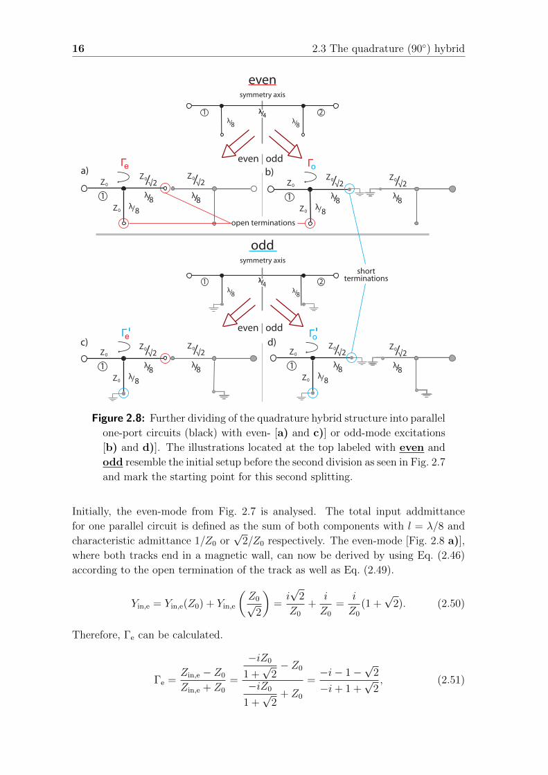
Figure 2.8: Further dividing of the quadrature hybrid structure into parallel
one-port circuits (black) with even- [a) and c)] or odd-mode excitations
[b) and d)]. The illustrations located at the top labeled with even and
odd resemble the initial setup before the second division as seen in Fig. 2.7
and mark the starting point for this second splitting.
Initially, the even-mode from Fig. 2.7 is analysed. The total input addmittance
for one parallel circuit is defined as the sum of both components with l = λ/8 and
characteristic admittance 1/Z0 or√
2/Z0 respectively. The even-mode [Fig. 2.8 a)],
where both tracks end in a magnetic wall, can now be derived by using Eq. (2.46)
according to the open termination of the track as well as Eq. (2.49).
Yin,e = Yin,e(Z0) + Yin,e
(Z0√
2
)=i√
2
Z0
+i
Z0
=i
Z0
(1 +√
2). (2.50)
Therefore, Γe can be calculated.
Γe =Zin,e − Z0
Zin,e + Z0
=
−iZ0
1 +√
2− Z0
−iZ0
1 +√
2+ Z0
=−i− 1−
√2
−i+ 1 +√
2, (2.51)

2 Microwave fundamentals 17
where the correlations Zin,e = 1/Yin,e and Γ = (A − Z0)/(A + Z0) are applied2 by
substituting the input impedance of the even-mode Zin,e.
The odd-mode [Fig. 2.8 b)] is identified accordingly, employing the Eqs. (2.46), (2.47)
and (2.49):
Yin,e = −i√
2
Z0
+i
Z0
=i
Z0
(1−√
2), (2.52)
where the path with characteristic impedance Z0/√
2 is terminated through an elec-
tric wall, resulting in the minus-sign. This is also visible in the equation for the
corresponding Γo:
Γo =−i− 1 +
√2
−i+ 1−√
2. (2.53)
Equation (2.42) and Eq. (2.43) can now be solved with substituting Eq. (2.51) and
Eq. (2.53) and expanding the equation to a common denominator:
b1e = 0 (2.54)
and
b2e =−1√
2(1 + i). (2.55)
Calculating the odd-mode from Fig. 2.7 follows the same procedure, and using the
appropriate signs for open and short terminations results in:
Γ′e =i− 1 +
√2
i+ 1−√
2, (2.56)
Γ′o =i− 1−
√2
i+ 1 +√
2. (2.57)
This allows the calculation of Eq. (2.44) and Eq. (2.45):
b1o = 0 (2.58)
and
b2o =1√2
(1− i). (2.59)
Substituting Eqs. (2.54), (2.55), (2.58) and (2.59) into Eqs. (2.38), (2.39), (2.40)
and (2.41) from Eq. (2.37), the S-parameters can be calculated and the resulting
scattering matrix, presented in Eq. (2.60), is in accordance with Ref. [11, 12].
S = − 1√2
0 i 1 0
i 0 0 1
1 0 0 i
0 1 i 0
(2.60)
2The expression for Γ resembles Eq. (3.1).

18 2.3 The quadrature (90) hybrid
The matrix is exactely as expected and the presented derivation indicates that the
performance of a quadrature hybrid is independent of absolute values, allowing for a
very flexible design easily adapted to the desired working frequency by adjusting λ.
A comparison of the quadrature relation ship (S212 = −1/2 and S31
2 = 1/2) proves
that for an excitation of port 1, power is fully diveded between the ports 2 and 3
(with half-power). Furthermore, the phase shift between the ports 1 and 2 is 90
and 180 for the ports 1 tor 3, confirmable by using S21 = iS31 for a 90 shift from
port 2 to 3 [23]. The relation between input I and output O is now well defined and
the quadrature hybrid fully characterized:
O = S I = − 1√2
0 i 1 0
i 0 0 1
1 0 0 i
0 1 i 0
1in
2in
3in
4in
=
1out
2out
3out
4out
. (2.61)

Chapter3Experimental techniques
This chapter introduces the general measurement setup and the sample package. In
Sec. 3.1, an overview of the experimental setup is given. Section 3.2 presents the
sample package, including common design parameters and material properties as
well as the sample (chip) fabrication. In Sec. 3.3, a measurement device, the TDR,
is introduced.
3.1 Measurement setup and equipment
In this section, the measurement setup used in this thesis is presented. Figure 3.1 il-
lustrates a typical setup for low temperature measurements which allow the analysis
of Nb circuits in the superconducting state. An actual picture is shown in Fig. 3.2.
The setup contains a network vector analyzer (VNA) at room temperature. The
VNA is linked with a PC for data collection. Via coaxial cables, the VNA is con-
nected to the sample package that is located inside a liquid helium bath cryostat.
The VNA measures the frequency-dependent transmission between two ports of the
sample package as described in Sec. 2.2. In this thesis, the network analyzer 8722D
from Hewlett Packard with two ports is used.
For low temperature measurements, the cryostat is a necessary device, allowing the
sample chip (Sec. 3.2.1) to be examined while its niobium (Nb) layer is in the super-
conducting state. The cryogenic setup consists of an insert placed inside a dewar.
Figure 3.3 contains a picture of the actual insert utilized during the experiments
with a sample package. In order to cool the sample, liquid Helium is slowly trans-
ferred from its container into the cryostat until the sample package is fully covered
in liquid 4He. The temperature of the bath is approximatley 4.2 K [24], and the
sample quickly thermalizes to this temperature. Since this value is well below the
critical temperature of Nb (approximately 9 K). The sample package is connected
with the top of the cryostat via eight semi-rigid coaxial cables. More information
in this regard is presented in Sec. 3.3. The cables can be separated into two types.
The one most commonly used for our experiments is the copper-clad stainless steel
cable from Astrolab. With regards to the hybrid ring, which requires four desirable
19

20 3.1 Measurement setup and equipment
PC VNA
sample
unused ports,
terminated with
50 Ω resistances
cryostat
liquid
Helium
VNA cables -
to and in
cryostat
cables to
and inside cryostat
liquid
Helium
Figure 3.1: Schematic overview of a typical low temperature measurement
setup with PC, VNA, cryostat and sample package. The photograph
shows the sample package with the side-mount SMA connectors used in
the beginning of this work.
identical connections, this type is prefered because there is a total of six of them di-
vided into three sets that are calibrated for the 8722D.1 The other set, consisting of
two pure stainless steel cables, has a higher loss per unit length, effectively reducing
the effect of multiple reflections caused by these cables. An overview showing data
for the different cable types is presented in App. C.
1Calibration includes cables to and inside the cryostat.

3 Experimental techniques 21
liquid helium vesselVNA transfer tube for liquid helium
valve
helium gas recovery linedewar with insert
coaxial cables
Figure 3.2: Picture of the lab containing VNA and cryostat.
connection
to turbopump
sample package
feedthrough flange
for coaxial cables
topview
semi-rigid
coaxial cables
temperature
control
feedthroughs for
coaxial cables
50 Ω resistance
Figure 3.3: Photograph of the cryostat insert.

22 3.2 Sample package
3.2 Sample package
This section covers the sample package: a structured chip amidst a printed circuit
board (PCB) that is assembled in a gold-plated copper box. A picture of the setup
can be found in Fig. 3.4. The chip in the center is connected to the PCB with
aluminum bonds. We explain general design parameters and material properties as
well as examine important characteristics and fabrication procedure where necessary.
3.2.1 Sample Chip and PCB
The sample is fabricated on a 12× 12 mm2 silicon (Si) substrate, which has a thick-
ness of 250 µm and is covered with a 150 nm thick layer of thermal oxide. It can be
either a calibration chip with several waveguides on it or it can contain a quadrature
hybrid structure. In both cases, the waveguides have a CPW design (see Sec 2.1)
and are patterned in a sputtered 100 nm thick Nb film using optical lithography.
The fabrication process takes place at the Walther-Meissner-Institut (WMI). An
overview can be found in App. A.
The PCB is a CBCPW as introduced in Sec. 2.1. It seves as a connection between
chip (through bonds) and cable connectors since it is difficult to attach the latter
directly to the chip. In this section, the PCB’s composition and material properties
are presented. The PCBs consist of a 635 µm thick dielectric layer of Rogers 3010
(see Ref. [25] for details on the substrate) which is covered from both sides with a
55± 5 µm thick, textured copper film. An exact value for the thickness of the copper
film is not available due to the uncertainty of the metallization process necessary to
create vias (see Fig. 3.5). Vias are metal coated holes2 that connect the conducting
layer at the bottom with the ground planes at the top, thus balancing the poten-
tial. Following Ref. [11], vias are expected to improve measurement performance
by suppressing parasitic parallel plate modes, a major cause of crosstalk between
adjacent circuits and thus a major source of leakage. Therefore, they are employed
in this thesis if/whenever possible. Typically, a PCB contains several hundreds of
vias accross the whole extent of the ground planes.
In general, it is desired that the characteristic impedance of the CPWs matches
50 Ω which is a standard for microwave equipment and used in all our measure-
ment setup and sample package components. With the characteristic impedance,
the ratio between width and gab of the CPW is immediately defined. Due to fab-
rication uncertainties by the company fabricating our PCBs, we deviate from 50 Ω
matching. In the case of press-contact type PCBs, previous design errors further
reduce matching quality especially for the unique PCB utilized during the experi-
ments presented in Sec. 4.1.1. More details on the used connector types and their
2In this case, copper is used for coating the vias. During the metallization process, the copper
thickness increases. The final thickness is not verified in this work because it is not particularly
important for the microwave properties of the PCB according to Sec. 2.1, although TXLine shows
a variation of the characteristic impedances for different thicknesses.

3 Experimental techniques 23
surface-mount mini-SMP connectors
box
aluminum
chip
PCB
press-contact SMA connectors
screw
bonds
textured
Figure 3.4: Picture of the entire sample package consisting of chip, PCB
and box. While screws keep the PCB in place inside the box, connection
to the chip is guaranteed through bonding. Shown are both PCB designs
with the appropriate connector types (see Sec. 3.2.2 for details). The
box is identical for either case and the PCBs have the same physical
dimensions.
respective designs specifics can be found in Sec. 3.2.2. Our sample package features
eight ports. Although only four of them are needed for the beam splitter, the other
four are important for later applications.
The dielectric layer consists of Rogers 3010, laminated ceramic-filled polytetrafluo-
rethylene (PTFE) composites provided by the Rogers Corporation [26]. The consid-
eration for Rogers 3010 as the substrate is based upon its application environment
at low temperatures. Under these conditions, one factor becomes more important:

24 3.2 Sample package
thermal expansion [13]. According to Ref. [26], Rogers 3010 has the same lateral
expansion coefficient of 17 ppm C−1 as copper3. Another advantage of Rogers 3010
is that the dielectric constants of Rogers 3010 and Si are very similar [see Ref. [27]
for εr,Si (T )]. A detailed analysis of the dielectric constant is presented in Sec. 4.1.3.
As discussed in Sec. 2.1, the configuration of a chip integrated within a PCB resem-
bles a double-layer structure and differing dielectric constants alter the performance
of the device. Through matching, these effects can be compensated and the com-
position is effectively reduced to a regular PCB, thus allowing for seperate analysis
and design of the components. The metal layer consists of copper, an element with
the second highest conductivity of all elements with 60 m mm−2 Ω−1 at 20 C [28],
thus approaching the assumption of a lossless medium made in Sec.2.1. The layer
thickness is at least 50 µm, which translates to at least 20 times the skin depth for
frequencies4 in the gigahertz regime (2 µm for 1 GHz according to Ref. [29]). Fur-
thermore, copper is resilient against atmospheric corrosion by building a protective
patina, has marginal low-temperature embrittlement and is available for a reason-
able price in high purity. The patina has to be removed at times. To this end,
we dip the PCB in a mixture of 1/3 weak formic acid and 2/3 deionized H2O for
10 s. Subsequently, it is put into a 70 C hot bath of Aceton tech., similar to the
processing of a chip. It is then washed with isopropylic alcohol and blow-dried with
gaseous N2. A clean surface is especially important when it comes to bonding.
3.2.2 Packaging
This section concentrates on the combination of the different components: packaging.
Furthermore, the two main PCB designs are presented since they require different
assembly techniques. In this regard, the appropriate connetors for each type are
introduced as well.
Initially, the integration and connection of PCB and sample chip are described.
In the center of the PCB, a square area with a side length of 12.2 mm is milled,
slightly larger than the chip itself. This tolerance allows for adjustements to the
chip placement. With a depth of approximately 250 µm, the surfaces of PCB and
chip are on the same level. PCB and chip are then combined through conglutination,
utilizing one drop of the AZ 5214 E resist as an adhesive. Finally, the metal surface
structures are linked electrically by bonding, connecting corresponding ground planes
or conductor tracks. At this point, separate steps follow for each design. They
are introduced and discussed in the following. Figure 3.5 gives an overview of the
different approaches.
One difference between the two PCB designs is important to note: for the PCB
with the surface-mount mini-SMP conenctors, all feed lines have the same length,
while in the press-contact design inner and outer feedlines differ by 1.3 mm. For the
3ppm=parts per million4For good conductors such as copper, the frequency dependency of the skin depth is proportional
to 1/√ω. Therefore, a reduction to 10% requires a 100 times larger frequency.

3 Experimental techniques 25
holes for screws to
x PCB inside the box
milled area
to contain
the chip
attachment
to connector
area to
be milled;
no vias
4 cm
4 cm
additional milling for chip adjustement during assembly
press-contact design with SMA connectors
chip
surface-mount design with mini-SMP connectors
0.4 mm
screw
mini-SMP
Figure 3.5: Layout (left) and photographs (right) of the press-contact and
surface-mount type PCBs.
mini-SMP PCB, the line between connector and chip is now approximately 15.5 mm
long. Without the 12× 12 mm2 long chip, the total length between two connectors
is 37.1 mm. The idea behind these specific lengths is to control the phase shift along
the conductor.
Press-contact connectors - SMA
This initially available PCB design [Fig. 3.5 a)] relies on press-contact SMA con-
nectors of the type 32K724-600S5 from Rosenberger (see Fig. 3.6 and data sheet
Ref. [30] or homepage Ref. [31] for more details) to link the PCB with the mea-
surement equipment or other hardware such as the cryostat. The PCB with chip
is placed inside the box and fixed in place with four screws located at the edges.
The box has two holes on each side to mount the connectors. Their center pins
fit through the holes and end directly above the PCB. A connection is then estab-
lishing by elevating the PCB. Therefore, screws at the bottom of the box directly
underneath the pins are tightened, thus pushing up the PCB and pressing it to the
connectors. Care has to be taken to avoid bending or breaking of the connector pin
in this process.

26 3.2 Sample package
connector
screw
pin
PCB
boxSMA
connector
screw
pin
SMA
cable
PCB
box
SMA connector
Figure 3.6: Left: schematic illustrating the functionallity of a SMA press-
contact connector. Right: photograph of the connector. The pin of the
SMA fits through a hole in the side of the box. Connection to the PCB
is accomplished by pressure through an elevating screw.
PCB
connectormini-SMP
box
cable
mating area with PCB (no vias!)
connectormini-SMPsoldering paste
Figure 3.7: Illustration and photograph of the surface-mount mini SMP
connector used in the new PCB design. It is soldered directly onto the
PCB, connecting both conductor and groundplanes this way. Also indi-
cated in the left figure is the adaptor, labeld as ’cable’.
Surface-mount connectors - mini-SMP
The second design utilizes the 18S101−40ML5 mini-SMP connectors from Rosen-
berger [32], compact surface-mounts that are 4× 4 mm2 wide. The full detent version
is chosen for a further increase in connection stability with a disengagement force of
approximately 29 N. Surface-mount connectors are soldered directly onto the PCB
as illustrated in Fig. 3.7. Therefore, a small amount of soldering paste5 is applied to
the PCB at the attachment areas and the connectors are positioned ontop. The PCB
is then placed on a hotplate for 10 to 12 seconds at 230 C. A positive side effect is
the self-adjustment of the connectors due to capillary forces. The soldering process
turns out to be reversible, i.e. it is possible to recover the connectors for a potential
later reuse. Careful handling is required when taking the PCB off the hot plate as
long as the soldering paste s still liquid to avoid unwanted displacement. After the
connectors are soldered to the PCB, the sample chip can be mounted and the PCB
is then placed inside the sample box. For linking the PCB with the remaining setup
that uses SMA connections entirely, a SMA/mini-SMP adaptor cable is necessary
(see Sec. 3.3). The PCB is fixed in the box with two screws. Furthermore, a lid for
the box suppresses air modes.
5No-Clean SMD-Lotpaste CR44 Sn62Pb36Ag (alloy) with flux FSW-32

3 Experimental techniques 27
ESM
SMA attachment
DSA
Figure 3.8: Photograph of TDR setup with DSA and ESM. The small
picture also shows the measured device connected to the TDR sampling
module.
3.3 Time Domain Reflectometry
TDR is used to measure impedances and impedance mismatches inside a device.
Impedance has already been recognized as an important indicator when it comes to
the properties of CPWs. But alternating impedances, for example at the connection
between two components, cause reflections. The associated reflection coefficient r is:
r =Z1 − Z2
Z1 + Z2
. (3.1)
Here, Z1 and Z2 are the impedances on either side of the connection. The TDR
makes use of this characteristic and detects reflection of a probe pulse as a function
of time. Figure 3.8 shows a picture of the device used in a typical setup. It consists of
a Digital Serial Analyzer (DSA) from Tektronix, the DSA8200 [33], and an Electrical
Sampling Module (ESM), the 80E08 [34]. For low-temperature measurements, the
ESM can be connected to the feedtroughs of the coaxial cables of our cryostat
containing the device under test.
In the following, we discuss a few fundamental TDR measurements on our devices.
In particular, we identify the position of physical objects such as the measurement
box or the PCB. First, it is important to recognize PCB and sample holder as
isolated devices as well as in a typical setup environment. Therefore, experiments
are done with and without a cryostat. The utilized PCB with press-contact SMA
connectors has no vias and only two straight CPW lines running accross. More
details on the PCB can be found in Sec. 4.1.2. Figure 3.9 a) focuses on the actual
PCB which is connected with the TDR through a 16” minibend coaxial cable. For a
full analysis, the data for the cable with and without the box is shown to confirm the
exact position of the box. Thereby, the following relation can be utilized to correlate
a time span ∆t with a length in position space using Eq. (2.19) or a comparative
calibration:
vph = λf (3.2)
28 3.3 Time Domain Reflectometry
In other words, the phase velocity vph is the product of the wavelength λ and the
frequency f . Note that the TDR has an internal delay of 42.5 ns. The PCB can be
clearly identified as a short flat section of the curve between two peaks indicating
the mismatch of the connectors. For the second setup, the box is placed inside the
cryostat to identify its position for later experiments when the PCB is intended to
match 50 Ω with low peaks from the connectors. Its characteristic impedance of less
than 43 Ω proves useful at this point, making the PCB very distinguishable from
the 50 Ω-matched cables of the cryostat. Figure 3.9 b) shows the TDR results for a
cryogenic situation, where the one waveguide inside the sample package is connected
to the ports 5 and 6 of the cryostat. In all these measurements, the external cable
length is determined through a calibration, using a 16” minibend (=> x) for a TDR
analysis (∆t). The resulting velocity is confirmed for several cables of the same
type. For the internal cryostat cables, we determine the phase velocity accoring to
the data sheet [35] and the measured ∆t. In Fig. 3.9 c), the effect one can see is that
the cables in the cryostat exhibit significant length differences. Hence most TDR
measurements presented in this thesis are modified by a suitable time offset to allow
for a better comparison of the results.
In the next experiment, we examine more closely the impedance inside the sample
package at low temperatures. The same PCB with press-contacts as in the previous
measurements is utilized, although this time a different waveguide inside the sam-
ple package is investigated. In Fig. 3.10, the TDR probing pulse is applied to the
waveguide in the sample package from opposite directions. For ideal connections
to the PCB, the curves are expected to be symmetric with respect to a vertical
axis through the midpoint of the waveguide on the PCB. While the PCB is indeed
symmetric, the mismatch of the connectors clearly differ from each other. Since the
signatures of the input connector are very similar, we identify most of this effect as
an artifact due to the strongly reduced probe signal reaching the second connector.
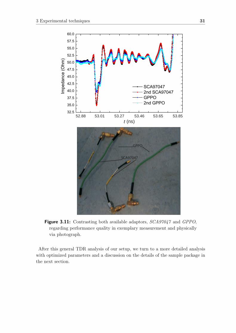
We next turn to a PCB with mini-SMP suface mount connectors. With the mini-
SMP connector type (Fig. 3.7), we use short SMP-SMA adaptor cables for the con-
nection to the SMA cables in the cryostat. Figure 3.11 shows TDR measurements
of the PCB for all adaptor cables available at that time. These belong to one of
the two types SCA97047-10 and GPPO [36]. The setup for these and the following
measurements contains a PCB with surface-mount connectors, connected with the
TDR via a 1 m long cable. The PCB does not contain a milled pocket for the chip.
The four adapter cables are each connected to a different waveguide on the PCB.
While different cables of the same model do perform similarly, there is a signifficant
discrepancy between the two adaptor cable types. The initial dip is more than 5 Ω
deeper for SCA97047 and the peak afterwars is almost 5 Ω higher. According to
Eq. (3.1), this results in a difference of reflection losses by more than 100% between
the adaptor cable types, assuming both features count as seperate reflection points.
In agreement with the different connector reflection properties, also the characteris-
tic ripples along the waveguide on the PCB are higher when the SCA97047 adaptor
cables.

3 Experimental techniques 29
0 100 200 300 400 50005
101520253035404550556065
410 415 420 425
46
47
48
49
50
a) b)
Impe
danc
e (O
hm)
x (mm)
PCB
box
a)
b)
cable with short
cable and box
42.5 43.46 44.42 45.38 46.35 47.31
t (ps)
approximately 40 cm
equal to 16” cable
46.44 46.5 46.54 46.59
c)
40 45 50 55 60 65 700
10
20
30
40
50
60
cryostat internal cable (5) with t = 10.3 ns; for v = 0.7 c, equals ~ 2 m
Impe
danc
e (O
hm)
t (ns)
42.5 ns; internal delay of TDR
t = 10 ns; corresponds to external cable to cryostat of 1 m se
cond
cab
le (6
)
press-contact PCB;both conductor ends linked with cryostat
59,5 60,0 60,5 61,0 61,5 62,0 62,5 63,0 63,5
35
40
45
50
55
60
cryostat port 1 cryostat port 2
Impe
danc
e (O
hm)
t (ns)
~ 34 cm
(ns)t
∆t = 10 ns
∆t = 10.3 ns
42.5 ns; internal delay of TDR
press-contact PCBcryostat cable (5);
equals ~2 m
for v = 0.7 c
corresponds to external cable of 1 m to cryostat
Figure 3.9: TDR experiments with the press-contact PCB from Sec. 4.1.2
out- and inside the cryostat. a) Sample package at room temperature
outside the cryostat. b) Low temperature analysis inside the cryostat.
The numbers in parentheses indicate the corresponding ports. c) The
length of the cryostat cabling can be deduced from the occurrence of the
characteristic PCB feature.

30 3.3 Time Domain Reflectometry
forwards
backwards
t (ps)61.49 61.73 61.97 62.21 62.45
(ns)t
waveguide midpoint
Figure 3.10: Impedance of the sample package measured from opposite
directions. Strongly asymmetric features (connectors) are encircled.
Because these ripples are artifacts due to multiple reflections, theit magnitude is
expected to roughly scale with the magnitude of the impedance mismatch at the
connectors acting as reflection points. In Fig. 3.12 a), connector, adaptors and the
PCB are marked. In accordance with the previous results, GPPO adapter cables
are utilized. In one measurement, the unused connectors at the opposing end of
the waveguide on the PCB is unattached and thus equal an open termination. For
the other, a second adaptor is connected instead. This data leads to the conclusion,
that the initial dip can be associated with the transition at the connector. Therefore,
the PCB is assumed to be located in between those features. The second experi-
ment, shown in Fig. 3.12 b), concentrates on the chip and is therefore conducted
at low temperatures. An area of the PCB is milled to include a calibration chip
with four parallel waveguides and both ends of the sample package are connected to
the cryostat with adaptor cables. The first measurement reveals the chip position.
It is distinctly and visbily positioned in the center of the PCB, bounded by two
peaks that mark the transition to and from it. The connection at the end of the
PCB cannot be seen because it is covered by the ripples already seen in Fig. 3.11.
The first connector signature designates the beginning of the PCB. In the second
measurement though, the PCB location, and thus the (relative) position of the chip,
is verified by showing both intersections with the connectors. Here, the connection
to the chip has improved so much compared to the other measurement, that the
transition to and from it can barely be seen at all. The data is presented in the
time domain because, depending on the position, there are different phase velocities
involved for the different media. For the external cabling, 62 ps roughly correspond
to 2 m, one each from cables to and inside the cryostat.
3 Experimental techniques 31
1080 1100 1120 1140 1160 118032,5
35,0
37,5
40,0
42,5
45,0
47,5
50,0
52,5
55,0
57,5
60,0
SCA97047 2nd SCA97047 GPPO 2nd GPPO
Impe
danc
e (O
hm)
x (mm)
GPPO
SCA97047
52.88 53.01 53.27 53.46 53.65 53.85t (ps) (ns)t
Figure 3.11: Contrasting both available adaptors, SCA97047 and GPPO,
regarding performance quality in exemplary measurement and physically
via photograph.
After this general TDR analysis of our setup, we turn to a more detailed analysis
with optimized parameters and a discussion on the details of the sample package in
the next section.
32 3.3 Time Domain Reflectometry
1100 1125 1150 1175 1200 1225 1250 127537,5
40,0
42,5
45,0
47,5
50,0
52,5
55,0
57,5
46
48
50
52
54
open 50 short
a) b)
Impe
danc
e (O
hm)
x (mm)
62,00 62,25 62,50 62,75
40
45
50
55
60
65 a) b)
Impe
danc
e (O
hm)
t (ps)
chip
PCB
mini SMP
connector
PCBadaptor cable
PCB with second adaptor
PCB (open termination)
a)
b)
53.08 53.3 53.56 53.8 54.04 54.3 54.52 54.8
chip transitionveri!cation measurement
t (ps) (ns)t
(ns)t
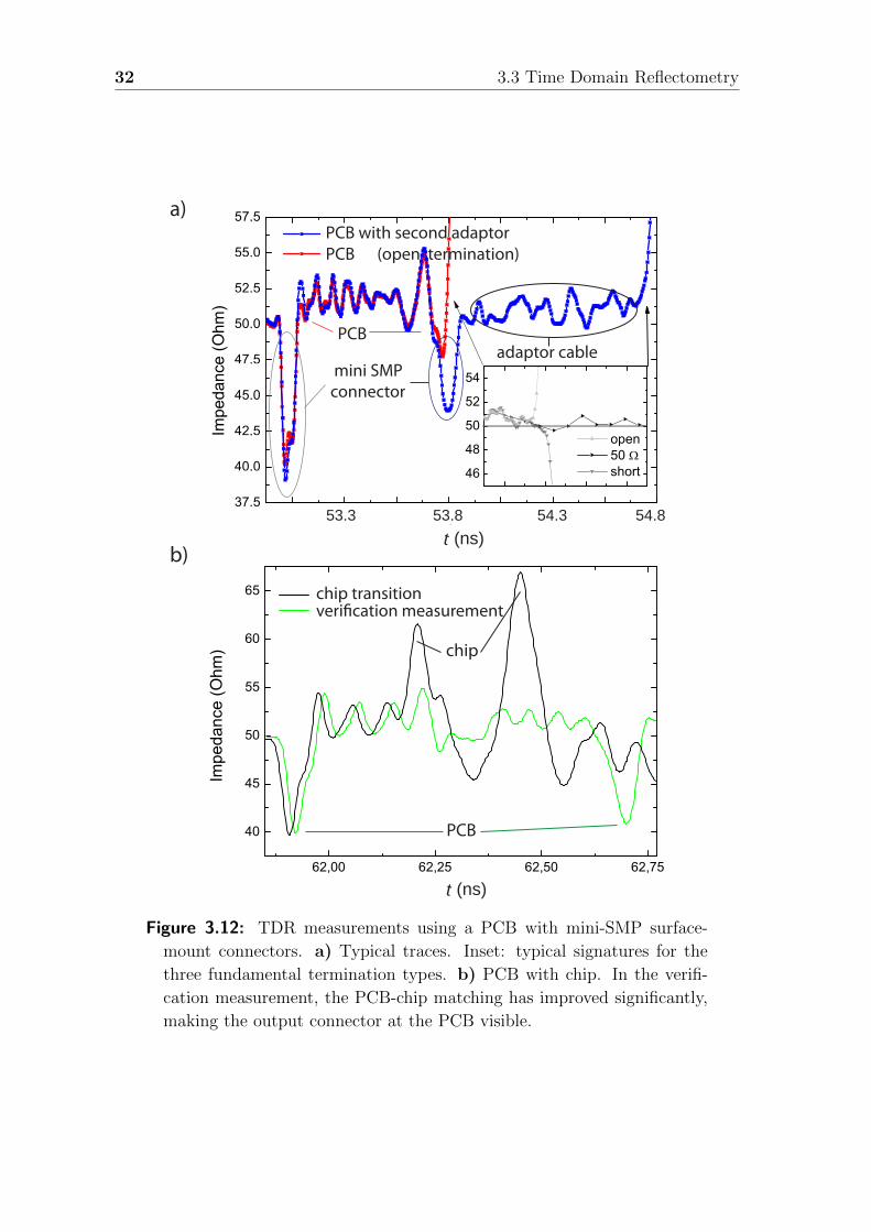
Figure 3.12: TDR measurements using a PCB with mini-SMP surface-
mount connectors. a) Typical traces. Inset: typical signatures for the
three fundamental termination types. b) PCB with chip. In the verifi-
cation measurement, the PCB-chip matching has improved significantly,
making the output connector at the PCB visible.

Chapter4Experimental results
In this chapter, the main results are presented and discussed. In Sec. 4.1, improve-
ment possibilities regarding the connections between the various components of the
sample package are examined and the different PCB designs from Fig. 3.5 are com-
pared. The 90 hybrid ring, as described in Sec. 2.3, is discussed in Sec. 4.2.
4.1 Characterization and optimization of the sam-
ple package
This section primarily addresses the PCB since it functions as the connection be-
tween actual sample, the chip, and the measurement equipment. First, a PCB with
press-contact connectors (see Fig. 3.5) is examined in Sec. 4.1.1. As a result, alterna-
tive approaches for improving the connection between setup and PCB are presented
and analyzed in Sec. 4.1.2. Section 4.1.3 employs the previous findings and combines
them with preliminary considerations in an alternative approach with the PCB. A
comparison of old and new design for the PCB is conducted in Sec. 4.1.4, com-
paring the performance and other crucial properties. Section 4.1.5 concentrates on
the remaining critical connection onto the chip, utilizing the new PCB design with
surface-mount mini-SMP connectors.
4.1.1 Analysis of press-connector sample holder
The starting point of this work is the quadrature hybrid measured during Michael
Fischer’s bachelor thesis [37]. The S-parameters of this device were measured using
the press-contact sample package shown in Fig. 3.4. However, the results were not
at all satisfactory as seen in Fig. 4.1. In particular, there is no frequency where the
S-parameters of the “direct” and the “coupled” port are close to 3 dB simultane-
ously. Therefore, we perform additional calibration measurements on this sample
package at low temperatures to get an overall impression of the performance or un-
cover potential design flaws.
33

34 4.1 Characterization and optimization of the sample package
The designs of the two used calibration chips are presented in Fig. 4.2. Figure 4.3
shows the corresponding data where several unexpected features confirm the pres-
ence of design problems. The setup for these experiments is the one presented in
Ch. 3.1: a transmission measurement through a PCB with chip, conducted in the
frequency domain and at low temperatures using the two lossy steel cables of the
cryostat. The utilized press-contact PCB can be found in Fig. 3.5 a). The design
parameters for the CPWs are w = 200 µm and g = 130 µm. The two ports of the sam-
ple package required for the transmission measurement are connected to the cryostat
cables 1 and 2. The other six unused ports are terminated with 50 Ω loads. The
performance observed is not satisfactory. Especially the large dip of −2.5 dB seen at
6 GHz is close to the desired working frequency of the beam splitter of 5.77 GHz (de-
fined through geometry, see Sec. 4.2). The utilized VNA calibration, which inlcudes
cables to and inside the cryostat, does not appear to be responsible for the features,
since the transmission is otherwise near 0 dB. One possible explanation for this
behaviour might be spurious resonances caused by multiple reflection points inside
the sample package. The most prominent candidates for such reflection points are
the connector-PCB transitions and the PCB-chip transitions. When checking the
resonant frequencies of various hypothetic half-wavelength resonators in our sample
package (see Fig. 4.4), we indeed find that they are close to the center frequencies
of the dips in Fig. 4.3.
For further clarification, the calibration chip is exchanged in favor of another design
[Fig. 4.2 b)]. As a result, we can see in Fig. 4.5 that the 6 GHz-dip, which we iden-
tified as most likely chip-resonance (see Fig. 4.3 and Fig. 4.4) changes significantly
while most other features don’t. We hence conclude that it is of utmost importance
to optimize the impedance matching between all components of the sample package
when working with open waveguide structures such as transmission lines or quadra-
ture hybrids.
Furthermore, the 0.5 dB offset between both measurements shown in Fig. 4.3 il-
lustrates a general problem with our setup. Reproducibility is not guaranteed and
cooldown-to-cooldown deviations are regularly encountered. A detailed examination
in this direction is conducted in Sec. 4.1.4.
The instructive analysis of calibration chips presented in this section enabled the
identification of weak points in the design of the sample package.

4 Experimental results 35
Figure 4.1: Data of hybrid ring measurement with kind permission from
Michael Fischer, conducted during his bachelor thesis [37].
a) b)
12
mm
12 mm 12 mm
Figure 4.2: Two calibration chip designs with different waveguide lengths
and characteristic impedance Z0 = 50 Ω. The corresponding parameters
are: width w = 200 µm and gap g = 100 µm.

36 4.1 Characterization and optimization of the sample package
measured
(GHz)f
12
mm
Figure 4.3: First frequency domain measurement using the calibration chip
design shown in inset from Fig. 4.2 a). The measurement path is denoted
in blue.
1 cm
Figure 4.4: Different paths to possible reflection points at intersections
using PCB with SMA connectors.

4 Experimental results 37
(GHz)f
12
mm
12 mm
Figure 4.5: Measurements with different calibration chip designs shown in
inset where measured transmission path is marked in blue.
4.1.2 Matching between PCB and SMA press-contact con-
nector
The first critical connection to be examined comprises the transition regions of a box
with SMA connectors and the PCB. In this section, several techniques to improve
the matching are discussed. The measurement series is devided into two parts. Ini-
tially, the transition from connector pin to PCB waveguide is analyzed. Then, we
examine how to best connect the corresponding ground planes, using the best result
from before. The performance is examined via time domain reflectometry measure-
ments, allowing for a direct analysis of the characteristic impedance. Finally, the
best result of the second series are compared with the initial setup from Sec. 4.1.1
to visualize the progress achieved.
For these experiments, a PCB with press-contact SMA connectors that is designed
especially for this particular task is utilized. To concentrate on the region in ques-
tion, no chip is incorporated since it would only complicate the analysis at this
point by introducing more reflection points. In addition, the PCB only contains
two waveguides with a width of 490 µm and gap 230 µm that are completely straight
to reduce the possibility of unwanted reflections at waveguide bends. A picture is
included in Fig. 3.1. With this critical component (chip) of a regular setup missing,
measurements with a vector network analyzer are not included at this point. With-
out a chip and therefore no superconducting component, this measurement series
can also be conducted at room temperature, approximately 293 K. Nevertheless, a
prototypical analysis at 4 K is done for one of the ports but not the whole series1.
1Low temperature measurements require a cryostat as described in Sec. 3.1.

38 4.1 Characterization and optimization of the sample package
Unused connectors are terminated with 50 Ω loads. There are no vias in this PCB.
A schematic of the PCB is shown in Fig. 4.6 and a picture of the general setup can
be seen in Fig. 3.8.2 The examined port is connected to a TDR sampling module
with a 16” minibend cable.
Connection between connector pin and PCB conductor
The first experiments concentrate on the center conductor of the CPW, and several
techniques are applied to improve the connevtivity between the PCB and the connec-
tor pin. Figure 4.6 shows a schematic of the setup for these measurements. One port
is the classical press-contact as described in Sec. 3.2.2 and no further improvements
are utilized. The opposite connector accross the conductor track is additionally
bonded to the CPW center conductor. For the second conducting lane, silver glue is
carefully applied with a toothpick to one connector, avoiding a connection between
center conductor and groundplane. At the second port, a small amount of soldering
paste is deposited on the connector pin and then heated with a hot air gun. This
technique proved to be disadvantegous as described at the end of this section. Box
and groundplane are ignored and not connected. The measurement data can be
found in Fig. 4.7.
a)b)
c)d)auxiliary )
additional
additive
bonds
silver glue
only pressureconnection
soldering paste
connector pin
box
PCB
4 cm
4 cm
Figure 4.6: Measurement setup for comparing different techniques of con-
necting the connector pin to the PCB waveguide center conductor with
each pin pressed to the board as shown in Fig. 3.6. While the first method
only relies on this type of connection, two bonds are further linking pin
and center conductor for the second. For the third, soldering paste is
utilized and silver glue is appliedto the final one. The materials of the
last two techniques are applied above and under the pin, after assembly
as described in Sec. 3.2.2.
2The PCB is concealed in a covered box for these experiments

4 Experimental results 39
426 428 430 432 434 436 438 44040
45
50
55
60
65
70 soldering paste silver glue press contact only bonds cable not attached
to PCB
Impe
danc
e (O
hm)
x (mm)
2020 2030 2040 2050 2060 2070 2080
40
45
50
55
60 293 K 4.2 K
Impe
danc
e (O
hm)
x (mm)
a)
b)
46.6 46.62 46.63 46.65 46.67 46.69 46.7 46.73
t (ps)
t (ps)61.92 62.02 62.12 62.21 62.31 62.4 62.5
(ns)t
(ns)t
Figure 4.7: Results of time domain reflectomertry measurement for various
connection methods of the center pin. a) Measurement series at room
temperature and b) one selected port (soldered connector) compared to
its results at 4.2 K.
According to the data presented in Fig. 4.7, soldering clearly depicts a prefer-
able connection possibility. Compared to the pure press-contact, the characteris-
tic impedance peak has decreased by approximately 10 Ω. The other techniques
are clearly inferior. Since they are also not very reproducible and, except for the
bonding, not stable during thermal cycling, we do not investigate them further. In
contrast, the thermal stability of the soldered connector is very good as we can see
from Fig. 4.7 b). A particular problem of the non-soldered connections resides in
the contact area between connector pin and PCB. The delicate pins do bend easily
(Fig. 4.8), especially when under constant pressure of the PCB. This in turn results
in a variation of the total mating surface, accordingly decreasing the connection

40 4.1 Characterization and optimization of the sample package
minor bending of SMA
connector pin
Figure 4.8: Picture of connector, showing a minor bending of the pin.
quality significantly. In some cases, the connection between press-contact connec-
tor and PCB is even lost during cool down because of differing thermal expansion
coefficients. This effect is visible in VNA measurements where the transmission at
low frequencies is drastically suppressed, resulting in a capacitive transission char-
acteristics as shown in Fig. 4.9. Additionally, open contacts can be confirmed with
a dc resistance measurement. The measured resistance accross the sample package
is then above a megaohm while a usual value would be approximately 67 Ω. In con-
clusion, it is assumed that most differences observed in Fig. 4.7 can be explained
with the unreliability of press-contact connectors. This is an issue that immediately
prevents reproducibility of measurement results and represents a main motivation
for switching to mini-SMP connectors.
Figure 4.9: Transmission measurement with the VNA. Graph is showing
the scattering parameter as a function of the frequency. In contrast to
the black curve, the red curve corresponds to an open connection. The
capacitive characteristic is most prominent in the shaded area. Taken
from his bachelor thesis with kind permission from Michael Fischer [37].

4 Experimental results 41
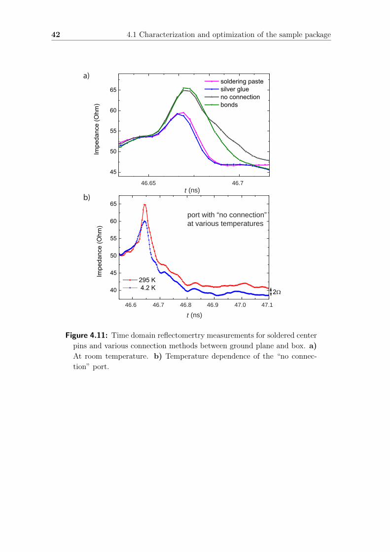
Contacting box and PCB ground planes
In the next measurement series, the effects of joining the ground planes of PCB and
connector, and therefore the box, are examined and the various techniques from the
previous serious are applied again and an identical setup is utilized. Here, all center
pins are soldered. A setup schematic is presented in Fig. 4.10. The ground planes
act as resonators as well and their huge width softens the boundary condition for
exciations. We compare the cases of no ground plane connection, bonded, silver-
glued, and soldered ground plane connection. However, the relatively large distance
of at least 1 mm between PCB and box complicates some of these approaches. For
the first scenario of a missing connection, there are no disruptions and the same is
the case for bonding. Silver glue, on the other hand, is problematic and has to be
applied in large amounts to actually bridge the gap. Soldering paste is also utilized
in larger quantities to cover a sufficient area, requiring more power for the necessary
heating process. The corresponding data is presented in Fig. 4.11. It can be seen
that a solid connection between ground plane and box does have a positive effect
on the impedance peak. For the initial peak, a decrease of more than 5 Ω can be
observed with increasing connection quality. Soldering proves to be the preferable
technique again, since the thermal stability of silver glue is questionable. The addi-
tion of bonds on the other hand seems to have no beneficial effect at all. It should
be noted that due to the box design, the bonds can only be applied further off the
conductors, a circumstance that is eventually deteriorating the comparison.
Figure 4.10: Schematic overview of ”ground plane connection” measure-
ment series experimental setup. The different techniques, applied in
the immediate neighbouring space of the conductor, are: no connection,
bonds, silver glue and soldering. All connector pins are soldered to the
center conductors.
42 4.1 Characterization and optimization of the sample package
430 432 434 436 438 44045
50
55
60
65 soldering paste silver glue no connection bonds
Impe
danc
e (O
hm)
x (mm)b)
a)
46.63 46.65 46.67 46.69 46.7 46.73
t (ps)
port with “no connection”at various temperatures
(ns)t
430 440 450 460 470 480
40
45
50
55
60
65
295 K 4.2 K
Impe
danc
e (O
hm)
x (mm)
2
t (ps)46.6 46.7 46.8 46.9 47.0 47.1
(ns)t
Figure 4.11: Time domain reflectomertry measurements for soldered center
pins and various connection methods between ground plane and box. a)
At room temperature. b) Temperature dependence of the “no connec-
tion” port.

4 Experimental results 43
Conclusion
We now compare the results from the Fig. 4.7 and Fig. 4.11 in detail. We find that
soldering is the preferred connection method for both center conductor and ground
planes. In addition, the quality of the soldered contact can vary when applying
excessive heat (air gun, see also Fig. 4.12) to the PCB. This is the reason why the
characteristic of “no ground plane” (Fig. 4.7) is a few ohm better than the “soldered
ground plane” characteristic in Fig. 4.11. However, the latter figure clearly demon-
strates that for a given situation, a solid connection between ground plane and box
is important.
A concluding summary is presented in Fig. 4.13, illustrating the progress during the
measurements above. The transition onto the PCB of the initial setup with pure
press-connection is compared to the best performing composition of this series: sol-
dered conductor and ground planes. Already in Fig. 4.13, the impedance mismatch
is reduced by 5 Ω despite an accidental mistreatment of the PCB. In the more op-
timistic approach of independently considering the effects of the two measurement
series of this section, the impedance mismatch could be reduced by 15 Ω. This cor-
reponds to a reduction of reflection losses by at least 10 % according to Eq. (3.1).
Nevertheless, the box-mount SMA connectors require to make the connections with
the PCB inside the box. This situation promotes problems such as excessive heating
of the PCB. Hence, we explore solder-on surface-mount connectors, which can be
placed on the PCB outside the sample box, in the next section.
regular color of Copper
discoloration of heated area
m250 m
Figure 4.12: Fotograph showing the degrading of the copper layer after
excessive heat exposure during the soldering process.

44 4.1 Characterization and optimization of the sample package
(ns)t
46.4 46.5 46.6 46.7 46.8
5 Ω
Figure 4.13: Overview of achievements during the connector-PCB match-
ing series. Comparison of first (red; see Fig. 4.7 with only pressure connec-
tion) and last measurement (green; from Fig. 4.11 with soldered conductor
and ground planes).
4.1.3 Design parameters and performance of PCBs with
surface-mount mini-SMP connectors
According to the results from the previous section, soldering is the preferable con-
nection type but also somewhat unreliable, possibly damaging the sample package.
To include this beneficial technique nonetheless while also avoiding the observed
negative effects, a new connector type is tested: the surface-mount mini-SMP. It is
designed specifically for this particular treatment, so no damage to this component
can be expected from the soldering process. The surface-mount connectors are sol-
dered to the PCB in a controlled way using a hotplate. The PCB is placed directly
on the hot plate without its box. Therefore, unnecessary heating can be avoided
because of the excellent thermal conductivity of copper. This minimizes the danger
of a deteriorated PCB performance.
In this section, a small summary is presented, giving an overview of general charac-
teristics of the design. But beforehand, Rogers 3010 is analyzed to guarantee that
the characteristic impedance of the designed waveguides is as close as possible to
50 Ω. Therefore, the PCB from Sec. 4.1.2 is reinvestigated with the focus on its
dielectric constant. In this way, we can verify equations, test calculation methods
and compare the measured data with the datasheet [25].
First, the TDR data for this PCB is shown in Fig. 4.14, where measurements at
room temperature (approximately 300 K) and at 4.2 K are presented for a soldered
connector pin and no ground plane connection. We can clearly identify the PCB
between the two peaks marking the connectors. Taking the average over the yellow

4 Experimental results 45
(ns)t
average value domain
physical PCB extent
Figure 4.14: Characteristic impedance for certain temperatures extracted
from TDR measurements. The measured port for all three experiments is
the same, and likewise is the connector; the PCB is the one used through-
out Sec. 4.1.2. The dashed line marks the possible physical extension of
the PCB.
Table 4.1: Characteristic impedance for certain temperatures extracted
from TDR measurements seen in Fig. 4.14 for soldered SMA connector
pin. Z0 for the pre-soldering PCB at 300 K is 43.5± 0.9 Ω.
4.2 K 300 K
39.9± 1.2 Ω 41.4± 0.5 Ω
region in Fig. 4.14, we can extract the characteristic impedance of the waveguide on
the PCB for both temperatures. The values are given in Tab. 4.1.
The equations presented in Sec. 2.1 are now employed and comared to the measured
data. The PCB itself is a single-layer CBCPW and its characteristic impedance Z0
is given by Eq. (2.18), using the expressions for εeff introduced in Eq. (2.20) and
Cair [Eq. (2.2)]. With the parameters for width (w = 490 µm), gap (g = 230 µm),
substrate thickness (h = 635 µm) and the distance to the lid (approximately h1 =
7000 µm), the k arguments can be calculated. According to Eq. (2.22), this gives
k3 = 0.51597 for the substrate and k = 0.51613 for air, so almost identical values.
Since both arguments are smaller than 1/√
2 = 0.70..., the approximation presented
46 4.1 Characterization and optimization of the sample package
in Eq. (2.5) can be used and the result is 0.767 for both values.3 Therefore, q as
defined in Eq. (2.21) is approximately 0.5, resulting in an effective permittivity of
5.6 for a dielectric constant of Rogers of 10.2 at room temperature as given by
the Rogers data sheet [25]. Accordingly, the characteristic impedance of the PCB
should be 51.4 Ω. This result differs significantly from the experimental value of
41.4± 0.5 Ω. Inserting the same parameters in the program TX-Line [38] (with
conductor thickness t = 35 µm), a characteristic impedance of 42.2 Ω is computed
for a CBCPW at 10 GHz (with regards to Ref. [25]). Changing the frequency to
20 GHz or 30 GHz, the possible bandwidths of the 80E08 ESM [34], only modifies
the result negligible. Using a permittivity of 10.5 on the other hand, a value included
in the domain of uncertainty provided by the Rogers Corporation, gives a character-
istic impedance of 41.7 Ω. This value is in excellent accordance(/agreement) with
the measured data and confirms the reliability of the program TX-Line which is
used from now on rather than analytical formulas to calculate design parameters.
To verify the dielectric constant of Rogers 3010 at low temperatures, the used per-
mittivity value is adjusted until the characteristic impedance matches the measured
data. For εr = 11.55, the measured impedance Z0 = 39.9 Ω can be realised. Con-
sequently, εeff changes to 6.275 for the above described q of 0.5. With Eq. (2.19)
and v = x/∆t, the marked area from Fig. 4.14 of ’length’ ∆t = 0.42 ns, utilized to
determine the average/mean value, corresponds to a phycisal length x of 5 cm. For
the real waveguide length of 4 cm, a time span of ∆t = 0.33 ns is determined instead,
using the same phase velocity.4 This leads to the conclusion, that the effect of the
connectors is even more significant than expected.
Figure 4.15 compares the results for the dielectric constant of Rogers 3010 evaluated
with TX-Line to the denominated values for the temperature dependency from the
Rogers 3010 data sheet [26] with a range of ±0.3, marked as the grey area. The
uncertainty of the measured numbers is an estimation, resulting from combined un-
certainties, for example when determing width and gap magnitudes with a range of
at least ±5 µm or the exact assignment of PCB and connectors made in Sec. 3.3.
The comparison shows that the measured values at low temperatures are close to the
range expected from an extrapolation of the datasheet values. Therefore, εr = 11.55
is used for width and gap evaluation with TX-Line, to accommodate the real mea-
surement environment of liquid Helium.
With regarads to the actual PCB design, where a metallization process is necessarily
included in order to creat vias, the effects of conductor thickness variation are cal-
culated as well. For a typical increase of the textured top metal facing from 35 µm
to 50 µm, the characteristic impedance Z0 is expected to further reduce by 0.8 Ω.
This change is not in consent with the assumption of copper being a nearly perfect
conductor and has not been considered in the discussion of the CPW presented in
3For an integral of the first order, only the term proportional to m is considered. Including the
second term with m2 as well would result in k3 = 0.79.4This actual time span is also included in the figure, but note that only the period can be
depicted with no specific starting point.

4 Experimental results 47
0 50 100 150 200 250 300
10,0
10,5
11,0
11,5
12,0
Die
lect
ric c
onst
ant
T (K)
ranging dielectric constant according to Rogers data sheet
evaluated from measurements using TXLiner
Figure 4.15: Measured temperature dependence of the dielectric constant
of Rogers 3010.
Sec. 2.1. Since values computed with TX-Line match well with the measured ones,
this prediction should be taken into account for new designs.
Furthermore, the waveguides on the PCB are assumed to have infinitely wide
ground planes because their width is not identical from a symmetrical perspective, a
circumstance not considered in detail, but also not explicitly included in the compu-
tation with TX-Line. Unfortunately, the exact equations used during computation
are unknown, so the possibility remains that typical numbers of a FWCPW are
taken into account indeed. In addition, the already mentioned dependency of con-
ductor thickness on characteristic impedance depicted during computation could at
least decrease the discrepancy between predicted and measured values. It should be
mentioned that not considering a top metal cover results in the same value of εeff and
an increased characteristic impedance of 51.9 Ω, see Ref. [11] for more information
about the derivation. This is in accordance with the measurements presented in
App. D.
In the following, the performance of several surface-mount PCBs is depicted to get
a general overview of what to expect and how to verify the design parameters. All
of these designs are as described in Sec. 3.2.1 and utilize the laminated substrate
Rogers 3010. According to the company doing the texturing and metallization,
metal thickness ranges between 50 and 60 µm. The resulting vias are approximately
400 µm in diameter (dependening on metallization) and have an identical distance
between one another of also 400 µm. Width and gap variations ensure a universal
characterization and a chip is not yet included.

48 4.1 Characterization and optimization of the sample package
(ns)t
average value domain
physical PCB extent
Figure 4.16: TDR analysis of surface-mount PCBs with various design
parameters for the CPWs, conducted at 4 K.
Table 4.2: Measured and computed characteristic impedance for the PCBs
presented in Fig. 4.16. For the computations, thickness of t = 60 µm
and permittivity εr = 11.5 are assumed. Note that only the width value
is directly given, the appropriate gap parameter can be extracted from
Fig. 4.16.
width parameter (µm) 315 330
measured impedance (Ω) 48.7± 1.4 48.2± 0.9
computed impedance (Ω) 52.8 52.1
The measured impedance for the PCB with w = 315 µm is 48.7± 1.4 Ω. The cor-
responding characteristic impedance for a CBCPW with εr = 11.5 and a thickness t
of 60 µm is 52.8 Ω. For t = 55 µm, an impedance of 53 Ω is calculated5. An overview
over all numbers, including the second examined design, is given in Tab. 4.2. Again,
a comparison of the marked area with the physical dimensions is conducted.
In order to achieve a characteristic impedance of 50 Ω, calculated using TX-Line,
a dielectric constant εr = 13 is necessary for the denoted values of w, g and t
(t = 60 µm) at 10 GHz. This result lies within the uncertainty of the measured
value with ±1.4 Ω.6 and corresponds to a physical conductor length x of 6 cm, while
the actual length is x = 3.7 cm. Therefore, using ∆t = x/v, the actual time span
5With regards to the uncertainty of the total copper thickness from additional layers during
metallization, other values for t are analyzed as well.6In order to achieve a characteristic impedance of 49 Ω, εr = 13.6 is required, but this value
appears unrealistically large at this point.

4 Experimental results 49
necessary for a wave with velocity vph to cross the PCB can be calculated. The
result equals only 62 % of the assumed extension for the average value domain with
1.16 ns. This again indicates a significant extension of the connectors in the time do-
main since the assumed extension of the PCB is derived from the results of Sec. 3.3.
For εr = 11.55, x would correspond to 22 cm! Although there is still a noticeable dis-
crepancy between the expected and the measured dielectric constant (see Tab. 4.2)
of the Rogers 3010 substrate, we also clearly see the positive effect of our careful
analysis. The characteristic impedance of the waveguide on the surface-mount con-
nector PCB is now much closer to the desired 50 Ω than that of the old press-contact
connector PCB. The ripples in the PCB section of the TDR traces can again be at-
tributed to multiply reflected probe pulses. This interpretation is supported by the
observation that the ripple amplitude is larger for the trace with larger connector
impedance mismatch.
4.1.4 Comparison between press-contact and surface-mount
connector sample holder
This section contrasts the efficiency of the two design approaches with the PCB:
press-contact and surface-mount connectors. This comparison can not rely solely
on the measured performance, but must also include other essential factors. These
consist of reproducibility in general, implementation techniques and their possible
reversibility. Included within the PCB is also a calibration chip as seen in Fig. 4.2 a),
with bonding between chip and PCB conductors and ground planes.
Reproducibility is a major criterion in our experiments. The setup with SMA con-
nectors (see Fig. 3.5) does not satisfy this crucial criterion. Evidence can be found in
Fig. 4.17, where the measured data of a 16” minibend cable (40.6 cm) connecting the
TDR with various ports of a PCB placed inside a box is shown. For these measure-
ments, connector and PCB are connected according to Fig. 3.6, with bonds linking
the corresponding ground planes. Most problems are accessible directly. First, when
assuming identical connectors, the supposedly identical connections (ports 1 through
3) result in very different data with in peak hights ranging between 70 Ω (port 1)
and below 65 Ω (port 3). This is a major problem because it prohibits reproducible
experimentations. Therefore, the method with pressure contacts is too unreliable,
sometimes even resulting in open contacts (see Fig. 4.9), and is also likely to damage
the sensible connector pins when elevating the PCB excessively. As for the perfor-
mance, the total mismatch of up to 20 Ω is rather unsatisfactory as well. In addition,
the PCB impedance is not 50, but 47.5 Ω.
In comparison, Fig. 4.18 presents the data for a PCB with mini-SMP connetors. For
these measurements, the PCB is cooled repeatedly below 77 K in liquid Nitrogen
to simulate consecutive low temperature experiments. After a reheating period of
approximately five minutes, its performance is analysed with the TDR. We find that
the discrepancy to the previous measurements reduces with every cycle after the

50 4.1 Characterization and optimization of the sample package
cableport 1port 2port 3
(ps)t46.546.446.3 46.6 46.746.2 46.8
(ps)t46.546.446.3 46.6 46.746.2 46.8
(ps)t46.546.446.3 46.6 46.746.2 46.8
(ps)t46.546.446.3 46.6 46.746.2 46.8
(ns)t
Figure 4.17: TDR measurement at room temperature of press-contact PCB
design (with chip) as seen in Fig. 3.5 a). Also included is the measurement
of the cable without the sample package, effectively resulting in an open
termination.
initial cooldown. This implies that the properties evolve towards a stable condition
after the inital shock, a behaviour that is in agreement with other cycling experi-
ments [39]. The overall abberation of less than 1 Ω is negligible. Higher difference
observed in b) are mainly a result of a shifting along the x-axis and not a variation
of the characteristic impedance. Note that the PCB has not been cooled ahead of
the first measurement.
Furthermore, there is of course the general performance of the connection tech-
nique. With regards to reflection losses, the transition areas are first examined with
the TDR. A comparison is shown in Fig. 4.19 of a press-contact type PCB as seen
in Sec. 4.1.1 and the surface-mount variation. It can be seen that with the switch
to mini-SMP connectors, the peak that marks the intersection onto the PCB can be
decreased from 20 Ω to 10 Ω. For the minimal measured peak reduction of 5 Ω, this
imples a reduction of reflection losses from 15 % to approximately 11 % according to
Eq. (3.1). The PCB’s deviating impedance already makes a complete redesign with
adapted width and gap parameters necessary. Furthermore, as the waveguide length
on the PCB are proven to be of importance (see 4.1.1), careful selection of these
lengths must be considered as well to avoid spurious resonances. This is achieved
within the surface-mount PCB type, designed to a phase shift of 260 between con-
nector and chip (15.5 mm) at 5.6 GHz (with εr = 11.55) and a more closely matched
characteristic impedance. As indicated during the analysis of Fig. 4.5, avoiding
spurious resonance is impossible throughout the whole measured frequency range
4 Experimental results 51
a)
b)52.5 52.7 52.9 53.1 53.3
-4
-2
0
2
4
1. Measurement 3. Measurement 7. Measurement 10. Measurement
Impe
danc
e (O
hm)
(ps)t
52.5 52.7 52.9 53.1 53.3 (ps)t
(ns)t
(ns)t
Figure 4.18: Results of thermal cycling measurements in liquid nitrogen at
77 K in a). For illustration, the difference of measurements correspondent
to the tenth one are plotted in b).
(0 GHz to 10 GHz) is impossible, but feasible in the important region around the
working frequency of the planned beam splitter. Regarding the performance, solder-
ing already proved to be a enhanced connection type, there is however the problem
of the heating process discussed in Sec. 4.1.2. Surface-mount connectors on the other
hand benefit from the adapted heat exposure which can be reduced to the required
minimum within a reproducible process, increasing the probability of retaining the
improved transition performance. In addition, any amount of (mini-SMP) connec-

52 4.1 Characterization and optimization of the sample package
PCB
connectormini-SMP
box
cable
connector
screw
pin
PCB
boxSMA
connector
screw
pin
PCB
boxSMA
cable
(ps)t
Figure 4.19: TDR data of the transition onto the PCB for a mini-SMP
connector and two exemplary measurements that correspond to the press-
contact PCB design without any connection enhancements.
tors can be assembled during one soldering process, although the required time may
vary by 10 − 20 % or rather a couple of seconds, further limiting damaging effects.
The overall performance quality of soldered connections is retained. In comparison,
the connectivity is improved, lowering reflection losses by approximately 15 % or a
mismatch reduction of at least 5 Ω respectively.
In conclusion, switching to a new PCB design using mini-SMP connectors proves
to be successful. It features the advantageous connection quality of soldering while
indicating to eliminate most negative effects due to the hot air gun by using a hot
plate instead. The new connectors further guarantee reproducibility and a reliable
connection is achieved. Therefore, a PCB with surface-mount mini-SMP connectors
is established as the new setup for the rest of this thesis, combining low reflection
losses with mechanical stability.

4 Experimental results 53
4.1.5 Analysis of PCB/chip connection with surface-mount
sample holder using mini-SMP connectors
With the discovery of a reliable connection method between setup, connector and
PCB, the next critical connection can be examined. In this section, the transition
from PCB to chip is analysed in a low temperature environment with a PCB of
the surface-mount type. Taking the asymmetry of the sample package into account,
the analysis of the upper two waveguides is necessary for a complete overview (see
Fig. 4.20). Both conductors as well as all four corresponding ports are measured
during the same cooldown. Therefore, a combination of GPPO and SCA97047
adaptors has to be used (illustrated in the picture presented in Fig. 4.21). Also, low-
loss copper-clad coaxial cables are used in the cryostat (see App. C). Unfortunately,
a false time frame for port 4 has been used, resulting in the uselessness of measured
data. In the following analysis, the inferior adaptor (port 3) has to be taken into
account as indicated in Fig. 3.11 where a discrepancy of up to 2 Ω is detected. How-
ever, the concluding analysis at the end of this section does consider this fact.
This series is devided again into separate center conductor and ground plane analysis
with four cooldowns for each component. With w = 290 µm and g = 490 µm, it is
close to an characteristic impedance of 50 Ω. Naturally, the PCB has to be adapted
by milling to accommodate a chip. Since the chip is arranged symmetrically, it is
sufficient to observe the top two waveguides. For better comparison with the ini-
tial setup, the calibration design presented in Fig. 4.2 a) is chosen again with the
corresponding dip encountered and verified in Sec. 4.1.1 which covers the working
frequency of the hybrid ring. Therefore, achievements in transition improvement
should have a distinct visual effect in transmission measurements. Differently from
Sec. 4.1.2, design and dimensions of the chip do not allow for different techniques
besides bonding though. The areas in question are simply to small for another ap-
proach, as is exemplified at the relevant points. As a result, only the number of
bonds, and thus the connectivity, is increased and the changes to transmission and
impedance measured. The data collection is again devided in conductor path and
ground planes.

54 4.1 Characterization and optimization of the sample package
symmetry axisconnected ports
Figure 4.20: To illustrate the symmetry, a picture is shown of the sample
package with calibration chip in an advanced state of the measurement
series. The superscribed ports have to be measured for a full analysis.
cryostat cables 4 and 2(resistive temperature detection)
measured port 4
Figure 4.21: Sample box inside the cryostat insert.
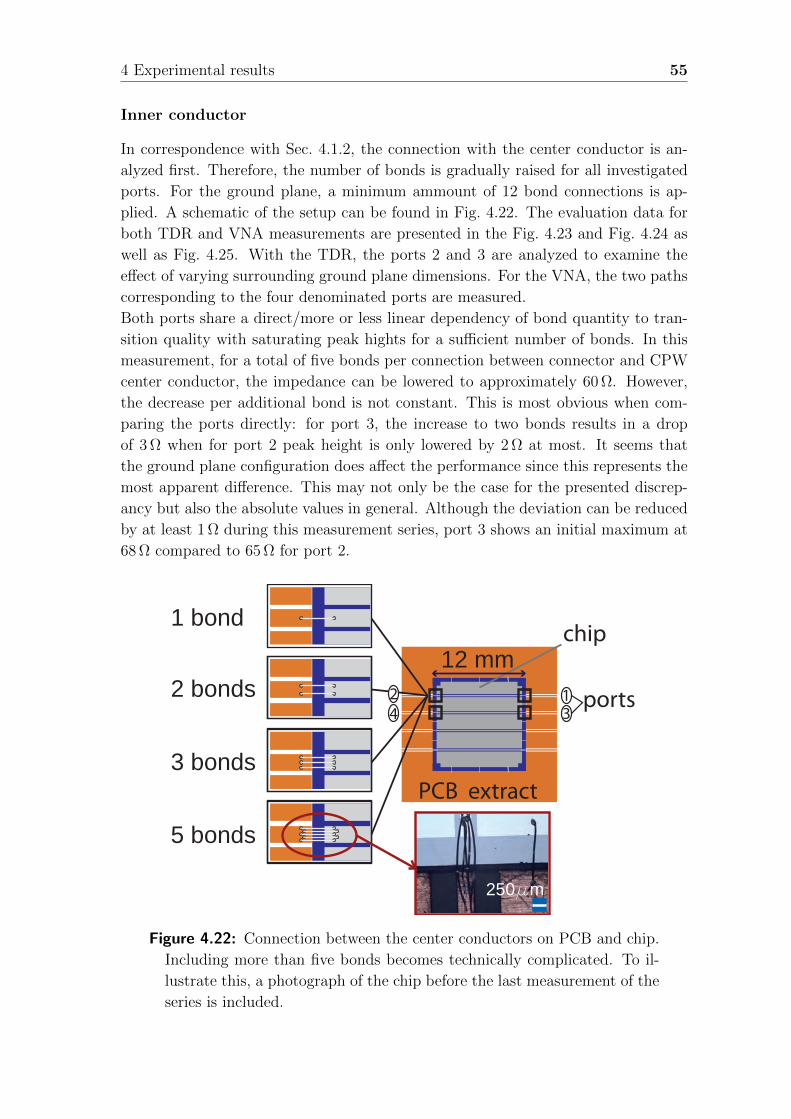
4 Experimental results 55
Inner conductor
In correspondence with Sec. 4.1.2, the connection with the center conductor is an-
alyzed first. Therefore, the number of bonds is gradually raised for all investigated
ports. For the ground plane, a minimum ammount of 12 bond connections is ap-
plied. A schematic of the setup can be found in Fig. 4.22. The evaluation data for
both TDR and VNA measurements are presented in the Fig. 4.23 and Fig. 4.24 as
well as Fig. 4.25. With the TDR, the ports 2 and 3 are analyzed to examine the
effect of varying surrounding ground plane dimensions. For the VNA, the two paths
corresponding to the four denominated ports are measured.
Both ports share a direct/more or less linear dependency of bond quantity to tran-
sition quality with saturating peak hights for a sufficient number of bonds. In this
measurement, for a total of five bonds per connection between connector and CPW
center conductor, the impedance can be lowered to approximately 60 Ω. However,
the decrease per additional bond is not constant. This is most obvious when com-
paring the ports directly: for port 3, the increase to two bonds results in a drop
of 3 Ω when for port 2 peak height is only lowered by 2 Ω at most. It seems that
the ground plane configuration does affect the performance since this represents the
most apparent difference. This may not only be the case for the presented discrep-
ancy but also the absolute values in general. Although the deviation can be reduced
by at least 1 Ω during this measurement series, port 3 shows an initial maximum at
68 Ω compared to 65 Ω for port 2.
1 bond
3 bonds
5 bonds
2 bonds
PCB extract
chip
4 31 ports2
m250 m
12 mm
Figure 4.22: Connection between the center conductors on PCB and chip.
Including more than five bonds becomes technically complicated. To il-
lustrate this, a photograph of the chip before the last measurement of the
series is included.

56 4.1 Characterization and optimization of the sample package
64,0 64,1 64,2 64,3 64,435
40
45
50
55
60
65
70
Impe
danc
e (O
hm)
t (ps)
61,9 62,0 62,1 62,2 62,335
40
45
50
55
60
65
70
1 bond 2 bonds 3 bonds 5 bonds
Impe
danc
e (O
hm)
t (ps) (ns)t
(ns)t
port 2
port 3
Figure 4.23: Low temperature analysis of setup from Fig. 4.22 for two ports
with TDR.
In Fig. 4.24 and Fig. 4.25, transmission measurements along the two paths are
shown in the frequency domain. We first notice a series of impressive dips in agree-
ment with the strong mismatch at the PCB-chip transition. We then notice the
significant difference between the spectra of the two paths, which we contribute
to the different ground plane configurations influencing the spurious resonances. In
Fig. 4.24, we see that the dip near 5 GHz shifts to lower frequencies with the increas-
ing number of bonds. This indicates that it is influenced by the boundary condition
of the bonds, making the “chip”-mode effectively longer because of reduced reflec-
tion effects. In Fig. 4.25 (for the other path), the depth of this dip is drastically
reduced and its width increased. Instead, a new dip appears near 3.5 GHz. This

4 Experimental results 57
5,0 5,5 6,0 6,5-30
-25
-20
-15
-10
-5
0
1 bond 2 bonds 3 bonds 5 bonds
S 21 (d
B)
f (GHz)
0 1 2 3 4 5 6 7 8 9 10-35
-30
-25
-20
-15
-10
-5
0
1 bond 2 bonds 3 bonds 5 bonds
S 21 (d
B)
f (GHz)(GHz)f
(GHz)f
12 mm
Figure 4.24: VNA data using setup presented in Fig. 4.22 showing S21,
the transmission between the ports 1 and 2, for different frequency spans
to give a total overview as well as analyzing performance close to the
working frequency of the future beam splitter.
indicates that the shallow wide dip is present as a “foot” feature also in Fig. 4.24
and corresponds to the “chip mode”. The comparatively narrow but deep dip could
be attributed to an effect of the ground planes. (We further support this idea later
when discussing the ground plane bonds.) Finally, we observe the characteristic
ripples due to reflections in the long low-loss cryogenic cables in the lower panel of
Fig. 4.25. Based on the results in this section, we believe that the PCB-chip con-
nection could be improved further by the use of ribbon bonds. Unfortunately, this
variant could not be investigated due to the lack of proper equipment.

58 4.1 Characterization and optimization of the sample package
5,0 5,5 6,0 6,5-4,5
-4,0
-3,5
-3,0
-2,5
-2,0
-1,5
-1,0
-0,5
0,0
0,5
1 bond 2 bonds 3 bonds 5 bonds
S 21 (d
B)
f (GHz)
0 1 2 3 4 5 6 7 8 9 10
-20
-15
-10
-5
0
1 bond 2 bonds 3 bonds 5 bonds
S 43 (d
B)
f (GHz)
S4
3
(GHz)f
(GHz)f
12 mm
Figure 4.25: VNA data using setup presented in Fig. 4.22 showing S43 for
different frequency spans to give a total overview as well as analyzing
performance close to the working frequency of the future beam splitter.

4 Experimental results 59
Ground planes
We next investigate the connection of the ground planes of chip and PCB. This situ-
ation is sown in Fig. 4.26. While bonds and maybe ribbon bonds are the only way of
connecting PCB and chip conductors, the ground planes have to be connected over
a much larger region. For the long edge (red square in Fig. 4.26), silver glue might
prove to be a viable possibility instead of using bonds, for it is large and distant
enough and as such not as frail for rough application. Soldering paste on the other
hand seems inappropriate for this purpose, even when using a hot plate. The heat
might destroy the sensible structure or at least influence the physical properties of
the dielectric. For this thesis, other possibilities are put aside and the general im-
portance of connectivity is examined instead through variation of bond quantity.
In this next measurement series, the effects of ground plane bonding on the general
performance at 4 K are examined. The total number of bonds is increased in four
steps from initially 12 to 184 in the last measurement. The setup for this ground
plane anylsis, more complex in its consistency than in previous measurements, has
to be divided into several regions. For comparable areas with respect to symmetry,
the amount of bonds is raised equally for each new measurement. These regions are
indicated in Fig. 4.26.
250 μm
3 12 25 58
0 2 4 6
1 3 5 8
measured
unused
4 3
12
Figure 4.26: The ground plane is divided into several sectors by the con-
ductors. Different characteristical areas are marked with an individual
colour. The total number of those bonds rises from 12 in the first mea-
surement to 50 for the second, then 96 and finally 184. The numbers
next to the areas represent the bond count of a region for the appropri-
ate measurement. Example photographs of the bonded sample are also
shown.
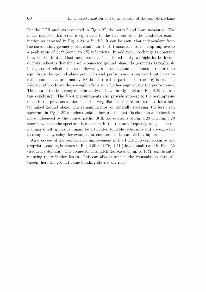
60 4.1 Characterization and optimization of the sample package
For the TDR analysis presented in Fig. 4.27, the ports 2 and 3 are measured. The
initial setup of this series is equivalent to the last one from the conductor exam-
ination as depicted in Fig. 4.23 ’5 bonds’. It can be seen, that independent from
the surrounding geometry of a conductor, both transistions to the chip improve to
a peak value of 55 Ω (equal to 5 % reflection). In addition, no change is observed
between the third and last measurements. The shared final peak hight for both con-
ductors indicates that for a well-connected ground plane, the geometry is negligible
in regards of reflection losses. However, a certain amount of bonds is required to
equilibrate the ground plane potentials and performance is improved until a satu-
ration count of approximately 100 bonds (for this particular structure) is reached.
Additional bonds are decreasingly effective in further augmenting the performance.
The data of the frequency domain analysis shown in Fig. 4.28 and Fig. 4.29 confirm
this conclusion. The VNA measurements also provide support to the assumptions
made in the previous section since the very distinct features are reduced for a bet-
ter linked ground plane. The remaining dips, or generally speaking, the less clean
spectrum in Fig. 4.28 is understandable because this path is closer to and therefore
more influenced by the unused paths. Still, the zoom-ins of Fig. 4.28 and Fig. 4.29
show how clean the spectrum has become in the relevant frequency range. The re-
maining small ripples can again be attributed to cable reflections and are expected
to disappear by using, for example, attenuators at the sample box inputs.
An overview of the performance improvement in the PCB-chip connection by ap-
propriate bonding is shown in Fig. 4.30 and Fig. 4.31 (time domain) and in Fig.4.32
(frequency domain). The connector mismatch decreases by up to 15 Ω, significantly
reducing the reflection losses. This can also be seen in the transmission data, al-
though here the ground plane bonding plays a key role.

4 Experimental results 61
64,0 64,1 64,2 64,3 64,4
40
45
50
55
60
65
Impe
danc
e (O
hm)
t (ps)
61,9 62,0 62,1 62,2 62,3
40
45
50
55
60
65 12 bonds 50 bonds 96 bonds 184 bonds
Impe
danc
e (O
hm)
t (ps)
port 2
port 3
(ns)t
(ns)t
Figure 4.27: TDR data for ports 2 and 3, using the setup presented in
Fig. 4.26 at low temperatures.

62 4.1 Characterization and optimization of the sample package
5,0 5,5 6,0 6,5
-20
-15
-10
-5
0
12 bonds 50 bonds 96 bonds 184 bonds
S 21 (d
B)
f (GHz)
0 1 2 3 4 5 6 7 8 9 10-35
-30
-25
-20
-15
-10
-5
0
12 bonds 50 bonds 96 bonds 184 bonds
S21
(dB
)
f (GHz)(GHz)f
(GHz)f
12 mm
Figure 4.28: VNA data using the setup presented in Fig. 4.26. Transmission
of different frequency ranges for S21.

4 Experimental results 63
0 2 4 6 8 10
-22,5
-20,0
-17,5
-15,0
-12,5
-10,0
-7,5
-5,0
-2,5
0,0
12 bonds 50 bonds 96 bonds 184 bonds
S 43 (d
B)
f (GHz)
5,0 5,5 6,0 6,5
-14
-12
-10
-8
-6
-4
-2
0
12 bonds 50 bonds 96 bonds 184 bonds
S 43 (d
B)
f (GHz)
(GHz)f
(GHz)f
12 mm
Figure 4.29: VNA data using the setup presented in Fig. 4.26. Transmission
of different frequency ranges for S43.
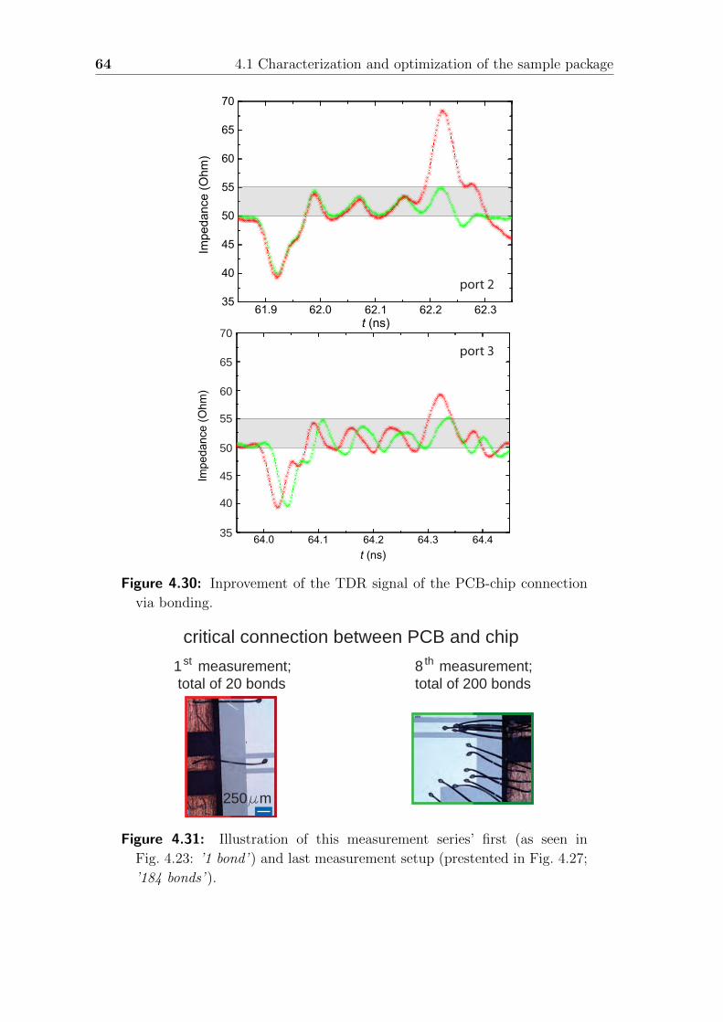
64 4.1 Characterization and optimization of the sample package
64,0 64,1 64,2 64,3 64,435
40
45
50
55
60
65
70
Impe
danc
e (O
hm)
64.0 64.1 64.2 64.3 64.4t (ns)
61,9 62,0 62,1 62,2 62,335
40
45
50
55
60
65
70
Impe
danc
e (O
hm)
61.9 62.0 62.1 62.2 62.3t (ns)
port 2
port 3
70
65
60
55
50
45
40
35
Figure 4.30: Inprovement of the TDR signal of the PCB-chip connection
via bonding.
critical connection between PCB and chip1 measurement; total of 20 bonds
8 measurement;total of 200 bonds
st th
m250 m
Figure 4.31: Illustration of this measurement series’ first (as seen in
Fig. 4.23: ’1 bond’ ) and last measurement setup (prestented in Fig. 4.27;
’184 bonds’ ).

4 Experimental results 65
12 mm
S
S
21
43
Figure 4.32: Transmission comparison of S21 and S43 for different frequency
spans. Progress between first (red) and last (green) measurement of the
series as presented in Fig 4.31 regarding the critical connection between
PCB and chip.
Conclusion
The performance analysis of press-contact and surface-mount connectors with the
TDR has already been presented in Sec. 4.1.4, where an overall advancement of at

66 4.2 The 90 hybrid ring
least 15 % in reflection losses could be recognized. In Fig. 4.33, a comparison of the
transmission through a calibration chip of the initial setup with press-contact PCBs
with the final from Fig. 4.32 (surface-mount connectors and 204 bonds between PCB
and chip) is presented. The narrow ripples are artifacts due to reflections in the ca-
bles. However, we have improved the performance of the PCB significantly in the
relevant frequency band and are now ready to investigate a quadrature hybrid in the
optimized sample package.
(GHz)f
S43
S43
S43
S21
Figure 4.33: Overview of the overall transmission for the initial setup with
SMA connectors presented in Fig. 4.3 (Sec. 4.1.1) and the results from
the final measurements using the surface-mount mini-SMP connectors for
S21 and S43 as seen in Fig. 4.32.

4 Experimental results 67
Figure 4.34: Design of the quadrature hybrid ring. With friendly permis-
sion from Michael Fischer [37].
Table 4.3: Design parameters of the measured quadrature hybrid seen in
Fig. 4.34.
characteristic impedance (Ω) Width (µm) Gap (µm)
Z0 = 50 34.4 20
Z0/√
2 = 35.4 125.2 20
4.2 The 90 hybrid ring
This section discusses the actual quadrature (90) hybrid which is in general a beam
splitter as described in Sec. 2.37. Figure 4.34 shows the layout used for optical
lithography (as explained in App. A) which is designed accordingly to the underlying
design properties that are also shown in Fig. 2.5 and Tab. 4.3. One notable feature
is the broadened waveguide towards the edges. The additional space gained by this
enlargement allows the placement of further bonds for an improved connection to the
PCB. With a width of 200 µm (gap = 100 µm), up to three bonds in close proximity
can be achieved. Utilizing the full length of this wider area, additional bonds can be
fitted onto the chip up to a total of at least five. Additionally, a surface-mount PCB
with a characteristic impedance of approximately 50 Ω is utilized in agreement with
Sec. 4.1.2 (the same PCB in fact). At transitions between waveguides of different
dimensions [11], width and gap are narrowed or widened consistently over a length
of 0.5 mm. This approach is also called tapering. In total, 150 bonds link PCB and
chip with five bonds used for each measured conductor and a total of 12 bonds to
connect the isolated section in the center of the hybrid ring structure with the other
ground planes of the chip, equally distributed to the (four) ground planes outside.
7A single quantum of light, the photon, has a 50 %-chance to appear on either side of the device.

68 4.2 The 90 hybrid ring
As decribed in Sec. 2.3, the central structure can be divided into two separate sections
with different characteristic impedances: Z0 and Z0/√
2. Each track has the same
length λ/4 = 5.172± 0.002 mm that is dependent on the working frequency8. They
are related through [40]:
λ =vph
f(4.1)
The variation of λ is a consequence of the different parameters for width and gap
in the two sections. They are listed in Tab. 4.3. However, a main problem is the
determination of exact permittivity values for Rogers 3010 as discussed in Sec. 4.1.3.
Furthermore, the exact behaviour at the T-junctions is unknown. This leaves it un-
clear, if λ is measured from the center of these junctions of conductors or equals the
length of the gap. The resulting minor variation is ignored at this point but has to
be remembered when judging the performance of the beam splitter.
Figure 4.36 shows the analysis of a hybrid ring at low temperatures conducted with
the four port VNA ZVA 24 and corresponding calibration measurements [41]. The
VNA is connected with the cryostat through 2 m long coaxial cables. To achieve
a good resolution, the frequency range of 9.99 GHz comprises 10.000 measurement
points with 500 Hz measurement bandwith of the IF-filter and an average number
of cycles 2. The power of the input signal is10 dB m.
To calibrate the VNA for the analysis of the hybrid ring, certain cable pairs have to
be connected and measured. Three of these pairs are necessary in order to obtain
a calibration for the three scattering parameters. Since no adaptors are available to
connect the SMA/GPPO adapter cables directly9, the question if the addition of a
sample package is necessary at this point does not arise. The setup for these mea-
surements is therefore equivalent to the one for the hybrid ring as seen in Fig. 4.35
but with other chip designs. Corresponding calibration chips are shown with their
measurements.
8The length, and therefore λ, is derived from design file; the possibility of an additional variation
has to be considered due to the uncertainty of the lithography process as described in App. A.9The lack of components is a major disadvantage of mini-SMP connectors.

4 Experimental results 69
-10 dB attenuators
Figure 4.35: Picture of the sample package in sample holder assembled in
the cryostat insertion with four GPPO adaptors, each combined with a
10 dB attenuator.
As already mentioned, the low-loss copper-clad cables of the cryostat are utilized.
Because they do not damp reflections well (see App. C), extra attenuators (IN-
MET 18AH-10dB) are added to each adaptor. Nevertheless, the calibration data
still contains resonances due to the structure of the calibration chip itself [see
Fig. 4.36 a)]. These features are relatively narrow and differ between calibration
chip and sample chip. Hence, a simple subtraction of the calibration data yields
artifacts in these regions. Fortunately, the relevant features of the quadrature hy-
brid are in a region where these artifacts are unimportant, so we use the calibration
anyways.
In Fig. 4.36 b) and Fig. 4.37 we can see that our device exhibits the expected be-
havior in the frequency window between 4.9 GHz and 5.8 GHz. In this region, the
signals of the “direct” and the “coupled” port are close to −3 dB while the isola-
tion is better than 9 dB. At suitable operation points, the latter can even exceed
15 dB. This is particularly true for the region around the designed frequency of
5.7 GHz. We attribute the remaining ripples to calibration issues, the fact that the
attenuators are not directly attached to the mini-SMP connectors (see Fig. 4.35),
remaining reflection points in the sample package, and our simple chip design (e.g.,
we have no microstructured metallic air bridges at the T-junctions). We expect that
improving some or all of these points will further increase the quality of our beam
splitter transmission data. We did not investigate the phase relation due to the un-

70 4.2 The 90 hybrid ring
kown electric length of the cryostat cables. Nevertheless, our measurements clearly
show the current design of our quadrature hybrid is, in principle, already suitable for
the construction of an interferometer consisting of two quadrature hybrids in series.
When additionally including a suitable Josephson-junction-based circuit, such an
interferometer can form the core of an all-optical quantum controlled-phase gate in
the microwave regime.
a)
b)
0 2 4 6 8-18
-12
-6
0
6
S21
S31
S41
Sj1 (d
B)
f (GHz)
0 2 4 6 8
-40
-30
-20
Sj1 (d
B)
f (GHz)
S21S31 S41
12
mm
Figure 4.36: a) Calibration measurements of the scattering parameters Sj1
for the sample package with the mini-SMP connector PCB; chip designs
shown in insets. b) Calibrated tansmisson through the quadrature hybrid
(Fig. 4.34). Shaded area to distinguish losses between 0 dB and 3 dB.

4 Experimental results 71
4,9 5,0 5,1 5,2 5,3 5,4 5,5 5,6 5,7 5,8-18
-15
-12
-9
-6
-3
0
S21
S31
S41
Si1 (d
B)
f (GHz)
Figure 4.37: Zoom into the relevant frequency range of Fig. 4.36 b).

72 4.2 The 90 hybrid ring

Chapter5Summary & Outlook
In this chapter, an overview of the progress achieved with the measurement setup
during this thesis is given. Furthermore, an outlook of future improvement possibil-
ities and applications is included as well.
During the analysis of the original setup with press-contact connectors (SMA) con-
ducted in Sec. 4.1.1, several critical aspects of the sample package could be disclosed
by examining the behaviour frequency domain measurements. This lead to the
examination of critical connections with the goal to reduce reflection losses. Experi-
menting with different techniques at the transition between PCB and measurement
setup (Sec. 4.1.2) resulted in a whole new design approach based on the employement
of soldered surface-mount mini-SMP connectors. This step constitutes one of the
main achievements of this thesis, since not only reflection losses could be reduced by
at least 10 %, but the new connector type also solves the major problem of a reliable
connection method and helps retaining a reproducible performance.
In addition, validating the parameters of the substrate Rogers 3010, especially the
dielectric constant, enabled the compensation of design errors of the PCB and al-
lowed for a matched characteristic impedance of 50 Ω with setup (cables) and chip.
Furthermore, the design of the waveguides on the PCB was optimized. Therefore,
a number of features in transmission measurements can be suppressed. In this part
of the thesis, there was also derived the direct dependency of connection quality
between the waveguides of PCB and chip (through bond quantity).
One problem encountered in Sec. 4.1.3 concerns the substrate of the PCB. Its dielec-
tric constant determines the characteristic impedance with direct consequences for
the design parameters and the accuracy of the employed calculation method. Via
TDR analysis, we find that the dielectric constant of the substrate at low tempera-
tures is close to the value extrapolated from the high-temperature dependence.
Finally, we embed a superconducting quadrature hybrid ring into our optimized
sample package. Transmission measurements clearly reveal the expected behavior
near the designed working frequency. This is a substantial improvement over the
work done in Ref. [37], where the same designa was measured in the unoptimized
sample package. A further increase of the performance could be given through the
73

74
application of additional bonds accross the gaps at conductor bends (T-junctions)
[9, 11]. Eventually, bonds added ontop of the chip could increase the potential bal-
ancing in a way similar to vias and therefore improve the performance as well, since
ground planes do effect the overall performance as proven in Sec. 4.1.5.
Based on the results presented in this thesis, the next steps towards a functional
interferometer can be taken. Ref [8] suggests a combination of two beam splitters
with a nonlinearity in between. This setup can then be utilized as a logic gate in an
all optical quantum computation device in the microwave regime.

AppendixAChip fabrication
The sample chip is a very flexible component since the characteristic impedance
of a CPW Z0 is dependent on geometry relations. Here, the fabrication process is
presented. Figure A.1 gives an overview over the production steps. To avoid con-
tamination, most steps (except for sputtering) take place in the cleanroom.
At the start of the production is the Si wafer (250 µm of intrinsic silicon coated
with 50 nm of thermal oxide) that constitutes the dielectric of the later coplanar
waveguide (pre-cut to 12× 12 mm2). Before further production steps can be taken,
a protective coat applied for transportation of the cutted dies has to be removed as
described in Tab. A.1.1 It is recommended to repeat this process before any produc-
tion steps are taken to avoid any dirt such as dust on the surface. Careful work is
important to avoid scratches on the sensitive surface.
In the next step, a Nb layer of 100 nm thickness is sputtered ontop the Si wafer.
Figure A.2 shows the custom build sputtering device at the WMI, and the process
parameters can be found in Tab. A.2. To avoid contamination, the setup is evacu-
ated to 10−9 mbar with separate sections (divided by doors) and a ‘Load Lock’ with,
when opened, continously flowing N2 gas. Transfers between the sections is possible
via a robotic arm.
During the sputtering process, atoms are ejected from the Nb target by ions gene-
rated from a magnetron (momentum exchange through collisions; sets off a cascade)
if their energy is larger than surface binding energy2. In the case of close proximity
between chip and target, thermal tensions may occur. This can cause that the metal
layer comes off (ultrasonic bath!).
The partial removal of Nb (”gaps”) is achieved through optical lithography and
reachtive ion etching (RIE). Figure A.3 shows the utilized equipment. At first, a
small amount of photoresist AZ 5214E [43] (approximately 15 µL) is applied to the
chip by spin-coating (see Tab. A.3), resulting in a film with a thickness of 1.4 µm [44].
1Before each bath, the chip is washed with the corresponding solvent of the following step. The
reason behind Isopropanol is that it boils away more easily then Aceton, leaving less residues and
is therefore better suited for a clean surface.2The sputtering rate is dependent on beam angle, distance between target and sample as well
as ions mass and energy.
75

76
b) Niobium sputtering c) resist coating
Nb Nb
Si Si
AZ 5214 E
d) exposure
Nb AZ 5214 E
Maske) etching f ) !nal chip
Si
a) Silicion wafer
Si
transparent
re"ective
Figure A.1: Production schematic that outlines the different manufacturing
steps necessary to produce a structured coplanar waveguide. Fabrication
overview: raw Si wafer a), with thin sputtered metal layer on top facing
b) and applied resist ontop the metal c); with mask d), after etching e)
and final CPW f). c) through e) illustrate the process steps of optical
lithography.
Table A.1: Cleaning proces
step 1 hotplate; in Aceton technical grade
time 1 h
temperature 70 C
step 2 ultrasonic baths
time 3 min
setting level 1; to avoid damage to the chip
solvent 1st bath Aceton technical grade
solvent 2nd bath Aceton por analysis
solvent 3rd bath Isopropanol por analysis
step 3 repeat steps 1 and 2
step 4 dry with gaseous nitrogen (N2)
However, this layer is not entirely flat but develops edge beads as illustrated in
Fig. A.3. The resist then has to be activated through baking: 110 C for 90 s. Dur-
ing this time, the molecules of the resist form a stable polymeric pattern according
to Ref. [45]. In addition, the remaining solvent concentration is reduced, avoiding
bubbles and other unwanted features, see Ref. [46] for more information.

A Chip fabrication 77
load
lock
transfer chamber
sputtering device
pump
control
Niobium
magnetron
sputtering controls
Figure A.2: Picture of sputtering device. With kind permission from Edwar
Xie [42]. Please note that the load lock is barely vbisible behind another
device.
Table A.2: Sputtering parameters for a 100 nm thick niobium layer
process pressure 4 · 10−3 mbar
magnetron power 200 W
pre− sputtering 300 s
sputtering time 240 s
Argon (process gas) flow 20
distance maximum
direction in front of magnetron (auto)
Table A.3: Spin coater settings
step 1
period 5 s
acceleration 500 rpm in 0.2 s
step 2
period 55 s
acceleration 8000 rpm in 6 s

78
a) b) c)
Figure A.3: Spin coater Delta 20 BM from BLE a), mask aligner MJB-
3 from Suss b) and Plasmalab 80 Plus reactive ion etcher from Oxford
Instruments c).
Substrate - SiNb
resist
after spin coating edge bead removal
Substrate - SiNb
resist
structure
Substrate - Si
resistNb
edge bead
texturing
masks
Figure A.4: Schematical overview of all the necessary removal processes
with corresponding masks that are textured with reflective and permeable
areas that let the light pass. During the final production steps, niobium
is removed from exposed areas where the resist has been activated.
The resist also contains photoactive compounds, making it sensitive to light. Expo-
sure with ultraviolet light of 400 nm [47] at an intensity of at least 36 mJ/cm2 breaks
the polymer chains of the resist. Since the output of the discharge lamp is subject to
variation, the corresponding time span has to be determined with a photodetector.
Where overexposure is not problematic (corners and edges), simply the maximum
of 99 s is used. The reason for these separate exposures are edge beads (see Fig. A.4
and App. B). The broken parts are then removed with the developer AZ 726 MIF,
see Tab. A.4. When this additional resist is removed from the edges (after develop-
ing), the mask with the actual design for the chip can be employed. 3 It should be
noted that in order to avoid undercuts due to overdeveloping, the actual structure
is developed less.
3This means, that the production for all chip designs is identical with the exception of the
utilized mask.

A Chip fabrication 79
Table A.4: Development
edges and corners (99 s exposure each)
time shaken in developer 150 s
time shaken in deionized water 30 s
idle period in deionized water variable; at least 100 s
structure (variable exposure time (36 mJ/cm2))
time shaken in developer 90 s
time shaken in deionized water 30 s
idle period in deionized water variable; at least 100 s
Edge beads are not not acceptable at this point because of absorption and reflection
inside the substrate and possible aggravation of resolution.
For a gap with width b, the angle dependent intensity is given by Ref. [48]:
I(β) = I0
sin
(πβb
λ
)πβb
λ
For an estimated tolerance ∆x of 1 µm and a gap h between mask and the central
surface level of the chip that is accoring to App. B4 approximately 200 µm,
β = sin(θ) = sin(arctan(∆x/h) = 0.013. The width b is dependent on the utilized
mask. For this analysis, the hybrid ring is used with b = 20 µm. For the wavelength
λ = 400 nm, the calculated value of the intensity at this angle is less than 0.5, so
insufficient for the resist to be activated. The corresponding value for ∆x = 2 µm is
0.6 and again smaller for ∆x = 5 µm.
The second possibility depicts a more direct approach: too much power is absorbed
or reflected if the resist layer is too thick. This leaves a thin film after developing.
When experimentating with narrower strips for the mask it is observed that the Nb
has not been fully removed. A photography of such an event can be found in App. B.
In the final step, the metal layer is removed with RIE [49]. The remaining resist acts
as a protective coat for the Nb and only areas where the resist has been removed
are etched away. For this step, SF6 serves as a process gas. During etching, a strong
electromagnetic field (radio frequency) is applied, ionizing the gas and creating a
plasma. The negative ions then drift towards the positive wafer platter, colliding
with the sample chip ontop where chemical reactions result in the removal of the
metal. After that, the resist is removed. On the one hand, this includes a cleanup
process as for the initial wafer, and a second treatment with the RIE called ashing
with O2 as a process gas. The chip is now finished.
4The measured values appear unrealistically large, almost the height of the chip itself. A possible
explanation could be poor resolution for thick objects since the measurement device, the DEKTAK,
is usually utilized to measure in the nm regime.

80

AppendixBResist layer thickness
Here, a side effect of spin coating square samples is examined: the edge bead. Dur-
ing the process, excessive resist is removed through centripetal force. However, this
results in an accumulation of resist at corners and, even more so, edges. These areas
have to be removed prior to the actual texturing. The consequence of inadequate
masks is presented in Fig. B.1, where a width of 0.3 µm proved to be insufficient. A
thin niobium strip remains between center conductor and ground plane, shortening
the circuit that is removed in a second exposure.
To determine the additional resist height after spin coating, a Dektak is used. With
it, variations in the surface structure of a sample can be examined. A stylus with
a tip radius of 12.5 µm is pressed against the surface with a force of 1 mg mm−2. In
order to measure the relative height, the stylus is moved across the sample and the
deflection is measured. Figure B.2 shows the utilized device at the Zentrum fur Nan-
otechnologie und Nanomaterialien (ZNN).
Nb strip 2 edge
removal
nd
Figure B.1: Photograph of a chip where the edge bead removal had to be
repeated on an already textured chip. The discontinuous dark grey area
at the bottom is resist that flew over while adhering chip and PCB.
81

82
Figure B.2: Picture of Dektak at the ZNN.
In the following, the effect of different accelerations during spin coating are an-
alyzed. The goal is to reduce the resist edge bead width and height in order to
minimize the necessary lift-off of niobium. If successful, a simple option is available
to modify the frequency of resonators on calibration chips (see Fig. 4.3). Therefore,
the initial step of the standard spin coater program is varied, compared to higher
settings and the difference δz then measured with the Dektak. The data for edges
and corners is presented in Fig. B.3.
Although the fitting is not perfect (central area should be flat), it is clear that the
desired effect does not occur. For an increased initial acceleration period, the peak
is assumed to shrink. However, the diagonal measurement from center to corner
unexpectedly shows the highest peak for the longest acceleration period of 400 ms
and a total speed of 1000 rpm. In the analysis of a horizontal line towards the edge
gives the medium setting as the largest result. Therefore, it can be summarized that
the plan of reduction failed since the expectations were not fulfilled. Other factors
seem to be more important in comparison. As expected, the additional resist height
at the edges lies fully within the exposed area of 0.5 mm (width), the extension of
the currently used mask1. It should be noted that since the resist thickness is the
highest at the corners, the smallest peak is expected to be at the measured center
of the edge.
For the diagonal measurement, the removed niobium is not sufficient in comparison
with the extensiveness of the corner edge bead. Since no texturing takes place at
this particular spot, this can be disregarded as the resist can be pressed flat so that
the mask has no additional distance to the surface.
The reduction of edge bead extension with varied acceleration settings failed, and
with the effects seen in Fig. B.1, no change of the mask design is possible.
1This magnitude seems unrealisctic. A resist thickness of up to four times the chip height is
probably a calibration error. However, substitution of µm in favour of nm does not affect the
conclusion of this measurement series (only the effect on exposure intensity is less drastic).

B Resist layer thickness 83
x
x
0 1 2 3 4 5 6 7 8-250
0
250
500
750
1000 500 rpm in 200 ms (standard) 750 rpm in 300 ms 1000 rpm in 400 ms
z (
m)
x (mm)
dust?
0 1 2 3 4 5 6
-100
0
100
200
300
dust?
z (
m)
x (mm)
500 rpm in 200 ms (standard) 750 rpm in 300 ms 1000 rpm in 400 ms
Nb removed
during lift-o!
corner acclivity
Figure B.3: Relative edge bead height at corners and edges measured with
Dektak.

84

AppendixCInternal cryostat cables
In the cryostat, two different sets of coaxial semi-rigid cables are contained: copper-
clad stainless steel (six) and stainless steel (two, numbered 5 and 6). The mini-bend
copper-clad stainless steel cables, Astro-Cobra-Flex 31086S [35], have an outer con-
ductor that is composed of 2 layers (each 0.0762 mm thick; inner oxygen-free high
thermal conductivity (OFHC) copper and type 304L stainless steel as the outer
layer) and a center conductor of copper clad steel [50] with a velocity of 0.7 c and
an optionally extended temperature range of up to −269 C. For the other cable
type, stainless steel constitutes the inner and outer layer. Further information is not
available.
Since all cables end in a male jack, sets of corresponding cables are linked for this
analysis via a female/female SMA adapter for calibration measurements. For this
comparison, the setup is cooled and the transmission measured. Before another cool
down, the connection between the cables is disengaged and then reconnected to sim-
ulate the exchange of the sample package. An overview of the deviating performance
properties is presented in Fig. C.1. An overall change in the transmission can be
observed of up to 0.4 dB which has to be taken into account with regards to consis-
tency. The first thing that appears when comparing both cable types is that it is
obvious that the steel cables have a higher attenuation of −10 dB to −20 dB across
the whole frequency range of 10 GHz. These additional losses result in the effect that
reflected signals provoke since these waves are further attenuated. As a result, oscil-
lations that overlay the original data experience a partial reduction as can be seen in
the direct comparison between 5 and 6 GHz within a 4 dB spectrum. Another effect
that can be observed is that there is a slight deviance of 0.2 dB between consecutive
measurements, a general problem of the utilized setup that reduces reproducibility
of measurements.
Additionaly, an actual sample is assembled inside the cryostat, cooled to 4 K and
connected with the different sets of the aforementioned cable types and the transmis-
sion between the corresponding ports i and j is measured. Utilized is a press-contact
PCB that also includes a calibration chip of the design shown in Fig. 4.2 b), linked
with the PCB through bonds. The data is presented in Fig. C.2. A shift towards
85
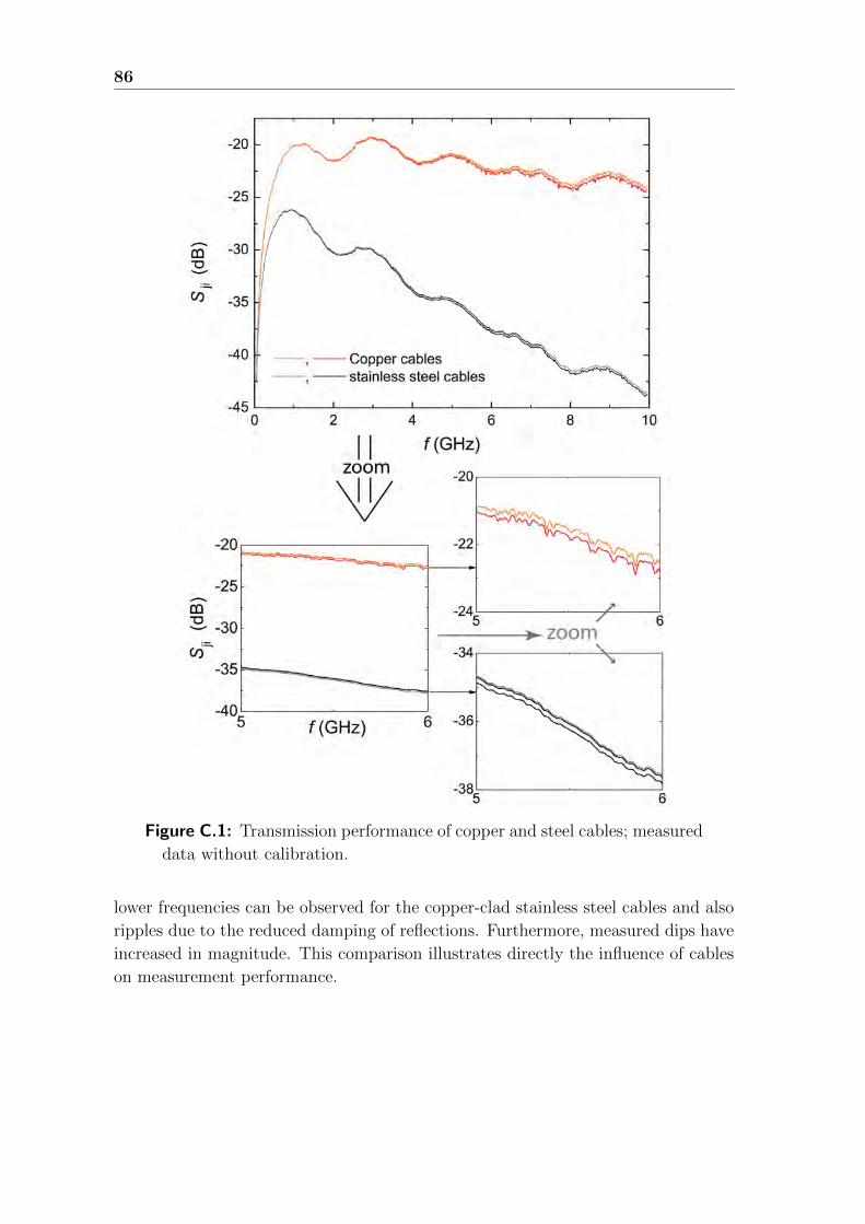
86
Figure C.1: Transmission performance of copper and steel cables; measured
data without calibration.
lower frequencies can be observed for the copper-clad stainless steel cables and also
ripples due to the reduced damping of reflections. Furthermore, measured dips have
increased in magnitude. This comparison illustrates directly the influence of cables
on measurement performance.
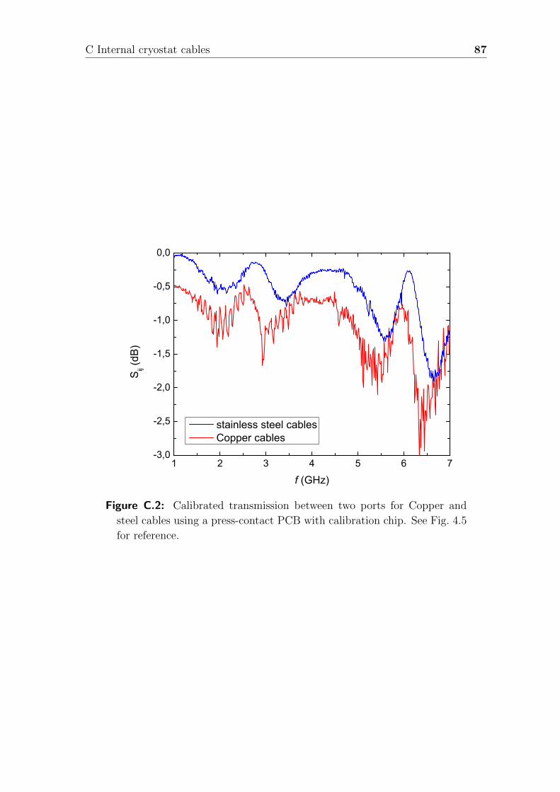
C Internal cryostat cables 87
1 2 3 4 5 6 7-3,0
-2,5
-2,0
-1,5
-1,0
-0,5
0,0
S ij (dB)
f (GHz)
stainless steel cables Copper cables
Figure C.2: Calibrated transmission between two ports for Copper and
steel cables using a press-contact PCB with calibration chip. See Fig. 4.5
for reference.

88

AppendixDBox top metal covers and air modes
Here, the effects of a varying air volumes are analysed with a press-contact PCB
assembled in a box. The top cover of the box is utilized to modify the available
space with εr = 1. Therefore, the original cover, an elevated metal plate, is compared
to the adapted version for the surface-mount design. A photograph can be found
in Fig. D.1. Please note that the necessary holes are not taken into account. An
additional metal plate, filling the space between the screw and the cover, is added.
Furthermore, the PCB is measured without a box cover.
As indicated during the analysis in Sec. 4.1.3, the effect for all volumes is negligible.
Figure D.1: Picture of top cover for a box that contains a surface-mount
PCB with holes for the adapter cables.
89

90
(ns)t
60.00 60.25 60.50 60.75 61.00 61.25 61.50
Imp
ed
an
ce (
Oh
m)
62
34
60
36
38
40
42
44
46
48
50
52
54
56
58no coverpress-contact coversurface-mount coversurface-mount cover with
additional plate
press-contact cover
coverssurface-mount covers
additional plate
(invisible: holes for adapter cables)
lower box half
PCB
Figure D.2: Effect of air volume variation on TDR performance by modi-
fication of top metal covers.

Bibliography
[1] R. Feynman and P. W. Shor, “Simulating Physics with Computers”, SIAM
Journal on Computing 26, 1484 (1982).
[2] D. Deutsch, “Quantum theory, the Church-Turing principle and the universal
quantum computer”, 400, 97 (1985).
[3] http://www.wmi.badw-muenchen.de/teaching/Lecturenotes/AS/AS2013_
Chapter10_1_Slides.pdf.
[4] I. Chiorescu, P. Bertet, K. Semba, Y. Nakamura, C. J. P. M. Harmans, and J. E.
Mooij, “Coherent dynamics of a flux qubit coupled to a harmonic oscillator”,
Nature 431, 159 (2004).
[5] A. Blais, R.-S. Huang, A. Wallraff, S. M. Girvin, and R. J. Schoelkopf, “Cavity
quantum electrodynamics for superconducting electrical circuits: An architec-
ture for quantum computation”, Phys. Rev. A 69, 062320 (2004).
[6] A. Wallraff, D. Schuster, A. Blais, L. Frunzio, R.-S. Huang, J. Majer, S. Ku-
mar, S. Girvin, and R. Schoelkopf, “Strong coupling of a single photon to a
superconducting qubit using circuit quantum electrodynamics”, Nature 431,
162 (2004).
[7] J. Clarke and F. K. Wilhelm, “Superconducting quantum bits”, Nature 453,
1031 (2008).
[8] J. L. O’Brien, “Optical Quantum Computing”, Science 318, 1567 (2007).
[9] H. Ku, F. Mallet, L. Vale, K. Irwin, S. E. Russek, G. Hilton, and K. Lehnert,
“Design and Testing of Superconducting Microwave Passive Components for
Quantum Information Processing”, IEEE Transactions on Applied Supercon-
ductivity 21, 452 (2011).
[10] C. Wen, “Coplanar Waveguide: A Surface Strip Transmission Line Suitable
for Nonreciprocal Gyromagnetic Device Applications”, IEEE Transactions on
Microwave Theory and Techniques 17, 1087 (1969).
91

92 BIBLIOGRAPHY
[11] R. N. Simons, Coplanar Waveguide Circuits, Components, and Systems (Wiley
Series in Microwave and Optical Engineering) (Wiley-IEEE Press, 2001), ISBN
0471161217.
[12] D. M. Pozar, Microwave Engineering (John Wiley & Sons, Inc., 1997).
[13] A. Marx and R. Gross, Festkoerperphysik (Oldenbourg Wissensch.Vlg, 2012),
ISBN 3486712942.
[14] E. Chen and S. Chou, “Characteristics of coplanar transmission lines on multi-
layer substrates: modeling and experiments”, IEEE Transactions on Microwave
Theory and Techniques 45, 939 (1997).
[15] C. Veyres and V. Fouad Hanna, “Extension of the application of conformal map-
ping techniques to coplanar lines with finite dimensions”, International Journal
of Electronics 48, 47 (1980).
[16] H. Klingbeil and W. Heinrich, “Calculation of CPW AC resistance and induc-
tance using a quasi-static mode-matching approach”, IEEE Transactions on
Microwave Theory and Techniques 42, 1004 (1994).
[17] S. Gevorgian, L. J. P. Linner, and E. L. Kollberg, “CAD models for shielded
multilayered CPW”, Transactions on Microwave Theory and Techniques 43,
772 (1995).
[18] J. Choma and W. Chen, Feedback Networks: Theory and Circuit Applica-
tions, Advanced series in circuits and systems (World Scientific, 2007), ISBN
9789810227708.
[19] M. Makimoto and S. Yamashita, Microwave Resonators and Filters for Wire-
less Communication - Theory, Design and Application (Springer, Berlin, Hei-
delberg, 2001), ISBN 978-3-540-67535-8.
[20] http://www.ittc.ku.edu/~jstiles/723/handouts/section_7_5_The_
Quadrature_Hybrid_package.pdf.
[21] http://de.scribd.com/doc/82883058/Chap-Coupler.
[22] www.ee.cityu.edu.hk/~eekleung/EE41139_notes/Lect7.ppt.
[23] http://www.google.com/patents/EP0643899A1?cl=en.
[24] Y. Zhang, J. R. G. Evans, and S. Yang, “Corrected Values for Boiling Points and
Enthalpies of Vaporization of Elements in Handbooks”, Journal of Chemical &
Engineering Data 56, 328 (2011).
[25] http://www.rogerscorp.com/documents/722/acm/
RO3000-Laminate-Data-Sheet-RO3003-RO3006-RO3010.pdf.

BIBLIOGRAPHY 93
[26] http://www.rogerscorp.com/acm/products/39/
RO3006-and-RO3010-Laminates.aspx.
[27] P. Lautenschlager, M. Garriga, L. Vina, and M. Cardona, “Temperature depen-
dence of the dielectric function and interband critical points in silicon”, Phys.
Rev. B 36, 4821 (1987).
[28] http://www.kupferinstitut.de/front_frame/frameset.php3?idcat=
233&client=1&idside=794&idcatside=1007&lang=1&parent=1.
[29] http://www.ivorcatt.co.uk/4_4.htm.
[30] http://rosenberger.de/ok/images/documents/db/32K724-600S5.pdf.
[31] http://rosenberger.de/ok/index.php?caller=xlink&url=detail.
php&&oldcaller=searchcritax&itemID=15176.
[32] http://rosenberger.de/ok/images/documents/db/18S101-40ML5.pdf.
[33] http://www.afc-ingenieros.com/uploads/Afc/Productos/Tektronix/
Manuales/Osciloscopios%20%20DSA8200/DSA8200%20-%20Digital%
20Serial%20Analyzer%20Quick%20Start%20User%20Manual%20-%
20071-2047-06.pdf.
[34] http://www2.tek.com/cmsreplive/psrep/13571/85G_13497_7_2008.05.
22.14.32.08_13571_DE.pdf.
[35] http://www.minibend.com/catalog_viewcable.asp?cnid=35.
[36] http://www.corning.com/gilbert/microwave_products/pushon_
interconnects/gppo.aspx.
[37] M. Fischer, “Supraleitende Mikrowellenstrahlteiler”, Bachelor’s thesis, Technis-
che Universitat Munchen (2012).
[38] http://www.awrcorp.com/products/optional-products/
tx-line-transmission-line-calculator.
[39] S. Myllymaki, J. Putaala, J. Hannu, H. Jantunen, M. Mantysalo, and E. Kun-
nari, “Failure mode characterization in inkjet-printed CPW lines utilizing a
high-frequency network analyzer and post-processed tdr analysis”, Progress In
Electromagnetics Research C 43, 1 (2013).
[40] H.-C. Hsu, K. Dasgupta, N. Neihart, S. Shekhar, J. Walling, and D. Allstot, in
Proceedings of 2010 IEEE International Symposium on Circuits and Systems
(ISCAS) (2010), pp. 1296–1299.
[41] http://www.rohde-schwarz.de/product/zva.html.

94 BIBLIOGRAPHY
[42] E. Xie, “Optimized fabrication process for nanoscale Josephson junctions used
in superconducting quantum circuits”, Master’s thesis, Technische Universitat
Munchen (2013).
[43] http://www.first.ethz.ch/infrastructure/Chemicals/
Photolithography/Data_AZ5214E.pdf.
[44] D. Reisinger, “Magnetit in ultradunnen, epitaktischen Schichtsystemen fur die
Spinelektronik”, Ph.D. thesis, Technische Universitat Munchen (2004).
[45] http://www.eng.buffalo.edu/Courses/ce435/Polymers/Photoresist.
[46] http://www.microchemicals.eu/technical_information/softbake_
photoresist.pdf.
[47] S. Dandl, “Herstellung und Charakterisierung einer definierten elektromagnetis-
chen Umgebung fur supraleitende Flussqubits”, Master’s thesis, Technische Uni-
versitat Munchen (2006).
[48] U. Zinth, Optik: Lichtstrahlen - Wellen - Photonen (Oldenbourg Wissensch.Vlg,
2005), ISBN 3486275801.
[49] http://www.aurion.de/plasmaanlagen-plasmaanlage/
rie-reactive-ion-etching.html.
[50] http://www.astm.org/Standards/B452.htm.