design and fabrication of centre frequency and bandwidth
TRANSCRIPT

Design and Fabrication of Centre
Frequency and Bandwidth Tunable
Cavity Filters
by
Mitra Nasresfahani
A thesis
presented to the University of Waterloo
in fulfillment of the
thesis requirement for the degree of
Master of Applied Science
in
Electrical and Computer Engineering
Waterloo, Ontario, Canada, 2014
c© Mitra Nasresfahani 2014


I hereby declare that I am the sole author of this thesis. This is a true copy of the thesis,
including any required final revisions, as accepted by my examiners.
I understand that my thesis may be made electronically available to the public.
iii


Abstract
To facilitate efficient utilization of limited and expensive frequency spectrum in commu-
nication systems, fully tunable filters are highly demanded. Realizing a constant absolute
bandwidth, a reasonable return loss, and a high Q value over a relatively wide tuning range
are some of the challenges in developing tunable filters for real system applications. This
thesis deals with the design and implementation of combline cavity filters with bandwidth
and centre frequency tunability. Cavity filters offers high Q and good power handling
capability.
This dissertation is organized in three parts. In the first part, we study the design
of constant absolute bandwidth tunable filters. We first design and implement a 5-pole
C-band Chebyshev tunable filter with 40 MHz bandwidth and frequency tuning range of
4.9−6 GHz. The inter-resonator coupling elements are realized using horizontal irises. The
fabricated filter exhibits a stable response over the tuning range with a bandwidth variation
of ±5.3%. We then exploit semi-vertical irises to realized adjacent coupling values in a 7-
pole X-band Chebyshev tunable filter with 80 MHz bandwidth and frequency tuning range
of 7− 7.9 GHz. The fabricated filter reveals a stable response over the tuning range with
a bandwidth variation of ±6.7%. We also show that using vertical irises, the normalized
coupling values remain almost independent of the cavity resonant frequency. This is in
contrast to horizontal or semi-vertical irises where a tedious optimization is required to
achieve the same goal.
In the second part, the objective is to design a fully tunable filter with wide tuning
range. To achieve bandwidth tuning, two tunable filters are cascaded. Due to the wide
tuning range and large bandwidth requirements, each individual filter can not maintain
a constant absolute bandwidth over the tuning range. Since only the cascaded response
matters, the concept of constant return loss design is introduced where the return loss
remains constant while the bandwidth could change over the tuning range. All the inter-
resonator coupling elements as well as normalized input and output impedances should
v

scale with the same factor in a constant return loss design. We show that this requirement
can be achieved by careful design of filter geometry for a 6-pole tunable Chebyshev filter
with tuning range of 1.8− 2.6 GHz. Despite the large bandwidth variation (±12.8%), the
return loss of the fabricated filter is better than 15 dB over the tuning range. Two of such
filters are then cascaded by an isolator to provide the bandwidth tunability. The cascaded
response exhibits a tunable bandwidth of 20− 100 MHz.
In the third part, the focus is on the design of a fully tunable two-port triplexer in
which three fully tunable bandpass filters are connected together through input and output
manifolds. After designing three fully tunable filters, manifold dimensions are optimized in
ADS circuit simulator. Simulation results show that the bandwidth and centre frequency
of each band can be independently tuned.
vi

Acknowledgements
I would like to express my sincere gratitude to my advisor, Professor Raafat Mansour for his
continuous guidance and encouragement throughout the course of my graduate studies. I
have had a great opportunity to work with him and have learned a lot from him throughout
the course of my MSc research. I wish to thank him for his support which was not limited
to research work.
It was such a great opportunity for me to be a member of the Centre for Integrated RF
Engineering (CIRFE) research group. I would like to specially acknowledge Dr. Siamak
Fouldai for always being available to provide guidance and for endless support; to Mostafa
Azizi for his valuable insight and fruitful discussions during these years; to Dr. Fengxi
Huang for his collaboration on this research; to Dr. Sara Attar for always encouraging
and listening to me and for being a great office-mate, and to Marco Iskandar for the joint
work on other interesting research topics. I am also indebted to Bill Jolley, the CIRFE lab
manager, for his support and friendship.
I would also like to recognize my colleagues Ahmed Abdel Aziz, Sormeh Sotodeh, Dr.
Neil Sarkar, Saman Nazari, Bahaedinne Jlassi, Desireh Shojaei, and Raisa Pesel. I would
like to extend my gratitude to all members of the CIRFE research group.
My warm wishes and thanks go as well to my dear friends Noushin Shiran, Bahador
Biglari, Alexandra Sevastianova, and many other friends who have enriched my life beyond
my studies.
I would like to thank my parents, Maryam Malekahmadi and Morteza Nasresfahani,
my brother Mohammad, and my grand mother Fereshteh Sajjadi for their support and
encouragement throughout my life. Last but not least, I would like to express my warmest
gratitude to my beloved husband, Akbar, for his endless support, patience, and encourage-
ments, without which I would not achieve this.
vii


To my beloved husband, Akbar,
for his dedicated support,
to my lovely boy,
and to my family.
ix


Table of Contents
List of Tables xv
List of Figures xvii
1 Introduction 1
1.1 Motivation . . . . . . . . . . . . . . . . . . . . . . . . . . . . . . . . . . . . 1
1.2 Objectives . . . . . . . . . . . . . . . . . . . . . . . . . . . . . . . . . . . . 2
1.3 Thesis Outline . . . . . . . . . . . . . . . . . . . . . . . . . . . . . . . . . . 3
2 Literature Review 5
2.1 Introduction . . . . . . . . . . . . . . . . . . . . . . . . . . . . . . . . . . . 5
2.2 Tunable Centre Frequency Filters . . . . . . . . . . . . . . . . . . . . . . . 7
2.3 Constant Bandwidth Tunable Filters . . . . . . . . . . . . . . . . . . . . . 8
2.4 Fully Tunable Filters . . . . . . . . . . . . . . . . . . . . . . . . . . . . . . 10
2.4.1 Fully tunable filters using extra elements for coupling adjustment . 10
2.4.2 Fully tunable filters based on dual band structures . . . . . . . . . 11
2.4.3 Fully tunable filters based on cascading two tunable filters . . . . . 13
xi

2.5 Tunable multiplexers . . . . . . . . . . . . . . . . . . . . . . . . . . . . . . 14
2.5.1 Tunable diplexers . . . . . . . . . . . . . . . . . . . . . . . . . . . . 15
2.5.2 Tunable triplexers . . . . . . . . . . . . . . . . . . . . . . . . . . . . 17
3 Tunable Filters with Constant Absolute Bandwidth 21
3.1 Introduction . . . . . . . . . . . . . . . . . . . . . . . . . . . . . . . . . . . 21
3.2 Design Principles . . . . . . . . . . . . . . . . . . . . . . . . . . . . . . . . 22
3.2.1 Theoretical Background . . . . . . . . . . . . . . . . . . . . . . . . 22
3.2.2 Tunable Resonator Design . . . . . . . . . . . . . . . . . . . . . . . 26
3.2.3 Inter-resonator Coupling Design . . . . . . . . . . . . . . . . . . . . 28
3.2.4 Input/Output Coupling Design . . . . . . . . . . . . . . . . . . . . 32
3.2.5 Design Optimization . . . . . . . . . . . . . . . . . . . . . . . . . . 33
3.3 5-pole Filter Design . . . . . . . . . . . . . . . . . . . . . . . . . . . . . . . 41
3.3.1 Resonator Design . . . . . . . . . . . . . . . . . . . . . . . . . . . 41
3.3.2 Inter-resonator Coupling Design . . . . . . . . . . . . . . . . . . . . 43
3.3.3 Input/Output Coupling Design . . . . . . . . . . . . . . . . . . . . 44
3.3.4 EM Simulation Results . . . . . . . . . . . . . . . . . . . . . . . . . 45
3.3.5 Measurement Results . . . . . . . . . . . . . . . . . . . . . . . . . . 45
3.4 7-pole Filter Design . . . . . . . . . . . . . . . . . . . . . . . . . . . . . . . 50
3.4.1 Resonator Design . . . . . . . . . . . . . . . . . . . . . . . . . . . . 50
3.4.2 Inter-resonator Coupling Design . . . . . . . . . . . . . . . . . . . . 51
3.4.3 Input/Output Coupling Design . . . . . . . . . . . . . . . . . . . . 53
3.4.4 EM Simulation and Measurement Results . . . . . . . . . . . . . . 55
3.5 Conclusions . . . . . . . . . . . . . . . . . . . . . . . . . . . . . . . . . . . 58
xii

4 Fully Tunable Bandpass Filters with a Wide Tuning Range 59
4.1 Introduction . . . . . . . . . . . . . . . . . . . . . . . . . . . . . . . . . . . 59
4.2 Objectives . . . . . . . . . . . . . . . . . . . . . . . . . . . . . . . . . . . . 60
4.3 Theoretical Background . . . . . . . . . . . . . . . . . . . . . . . . . . . . 61
4.3.1 Constant Return Loss Filter Design . . . . . . . . . . . . . . . . . . 61
4.3.2 Cascading Element Design . . . . . . . . . . . . . . . . . . . . . . . 63
4.4 6-pole Filter Design . . . . . . . . . . . . . . . . . . . . . . . . . . . . . . . 65
4.4.1 Design . . . . . . . . . . . . . . . . . . . . . . . . . . . . . . . . . . 66
4.4.2 Measurement and Test Results . . . . . . . . . . . . . . . . . . . . 69
4.5 Conclusions . . . . . . . . . . . . . . . . . . . . . . . . . . . . . . . . . . . 76
5 Fully Tunable Two Port Triplexer Design 77
5.1 Introduction . . . . . . . . . . . . . . . . . . . . . . . . . . . . . . . . . . . 77
5.2 Objective . . . . . . . . . . . . . . . . . . . . . . . . . . . . . . . . . . . . 78
5.3 Proposed Method . . . . . . . . . . . . . . . . . . . . . . . . . . . . . . . . 78
5.4 Filter Design . . . . . . . . . . . . . . . . . . . . . . . . . . . . . . . . . . 80
5.4.1 Coupling Routing Diagrams . . . . . . . . . . . . . . . . . . . . . . 80
5.4.2 Low Pass Filter Design . . . . . . . . . . . . . . . . . . . . . . . . . 83
5.4.3 High Pass Filter Design . . . . . . . . . . . . . . . . . . . . . . . . 88
5.5 Manifold Design . . . . . . . . . . . . . . . . . . . . . . . . . . . . . . . . . 95
5.6 Simulation Results . . . . . . . . . . . . . . . . . . . . . . . . . . . . . . . 96
5.7 Conclusions . . . . . . . . . . . . . . . . . . . . . . . . . . . . . . . . . . . 98
xiii

6 Conclusions 99
6.1 Contributions . . . . . . . . . . . . . . . . . . . . . . . . . . . . . . . . . . 99
6.2 Future Work . . . . . . . . . . . . . . . . . . . . . . . . . . . . . . . . . . . 101
APPENDICES 103
A TULA motor control 105
Bibliography 109
xiv

List of Tables
3.1 Cubical resonator’s dimensions. . . . . . . . . . . . . . . . . . . . . . . . . 42
3.2 Optimized iris sizes to attain constant coupling for different coupling values. 43
3.3 Probe dimensions for constant input/output coupling. . . . . . . . . . . . . 44
3.4 7-pole resonator’s dimensions. . . . . . . . . . . . . . . . . . . . . . . . . . 50
3.5 Optimized iris dimensions to achieve constant normalized couplings in the
7-pole Chebyshev tunable filter. . . . . . . . . . . . . . . . . . . . . . . . . 52
3.6 Probe dimensions for constant input/output coupling. . . . . . . . . . . . . 54
5.1 Frequency and bandwidth tuning requirement for the two port triplexer . . 78
xv


List of Figures
2.1 The side view of in-line irises . . . . . . . . . . . . . . . . . . . . . . . . . . 9
2.2 Measured tuning performance . . . . . . . . . . . . . . . . . . . . . . . . . 10
2.3 2-pole tunable filter and its circuit model . . . . . . . . . . . . . . . . . . . 10
2.4 Measured Fully tunable 2-pole filter performance. . . . . . . . . . . . . . . 11
2.5 Equivalent circuit model of dual-band combline filter . . . . . . . . . . . . 12
2.6 Measured bandwidth tuning performance . . . . . . . . . . . . . . . . . . . 12
2.7 4-pole elliptic filter structure using long and short irises . . . . . . . . . . . 13
2.8 Cascaded fully tunable filter transmission response . . . . . . . . . . . . . 14
2.9 Schematic layout of the tunable diplexer . . . . . . . . . . . . . . . . . . . 15
2.10 Measured results of tunable diplexer . . . . . . . . . . . . . . . . . . . . . 16
2.11 Triplexer filter bank layout . . . . . . . . . . . . . . . . . . . . . . . . . . . 18
2.12 Tuning response of three tunable filters in a filter bank . . . . . . . . . . . 18
2.13 Two port triplexer layout . . . . . . . . . . . . . . . . . . . . . . . . . . . 19
2.14 Triplexer filter bank layout . . . . . . . . . . . . . . . . . . . . . . . . . . 20
3.1 Impact of λ variations on filter shape for a six pole filter with BW =
100 MHz and RL = 20 dB: The coupling matrix M and the normalized
impedance matrix R are held constant in the tuning range. . . . . . . . . . 23
xvii

3.2 Combline tunable resonator with tuning disk . . . . . . . . . . . . . . . . . 27
3.3 Schematic diagram of two coupled resonators using horizontal iris. . . . . . 28
3.4 Normalized coupling variation vs. gap in a horizontal iris for different iris
heights. . . . . . . . . . . . . . . . . . . . . . . . . . . . . . . . . . . . . . 29
3.5 An iterative procedure to optimize the horizontal iris dimensions to achieve
a constant normalized coupling. The same procedure can be applied to
optimize the input/output probe dimensions. . . . . . . . . . . . . . . . . . 30
3.6 Schematic diagram of two coupled resonators using a vertical iris. . . . . . 31
3.7 Normalized coupling variation vs. gap in a vertical iris for different iris
openings. . . . . . . . . . . . . . . . . . . . . . . . . . . . . . . . . . . . . 32
3.8 Schematic diagram of the input/output resonator loaded with a long probe 33
3.9 Group delay peak variation vs. resonant frequency for different Lpr values. 34
3.10 Schematic of the coarse model in ADS simulator . . . . . . . . . . . . . . . 36
3.11 HFSS simulation of inter-resonator coupling vs. iris window length . . . . . 37
3.12 HFSS simulation of normalized input/output impedance vs. probe length. 38
3.13 EM model for calculating resonant frequency, including the effect of irises. 39
3.14 Self-resonator coupling versus the Gap calculated from HFSS simulation
results. . . . . . . . . . . . . . . . . . . . . . . . . . . . . . . . . . . . . . . 40
3.15 Coupling-routing diagram of the 5-pole filter. . . . . . . . . . . . . . . . . . 41
3.16 The resonant frequency and unloaded Q versus gap size: HFSS simulation
result . . . . . . . . . . . . . . . . . . . . . . . . . . . . . . . . . . . . . . . 42
3.17 EM simulation results of adjacent normalized coupling over the tuning range 43
3.18 EM simulation result of group delay over the tuning range. . . . . . . . . . 44
3.19 EM model of 5-pole tunable filter. . . . . . . . . . . . . . . . . . . . . . . . 45
xviii

3.20 EM simulated tuning performance of the 5-pole filter . . . . . . . . . . . . 46
3.21 Fabricated 5-pole bandpass tunable filter. . . . . . . . . . . . . . . . . . . . 47
3.22 Measured tuning response of the 5-pole tunable filter. . . . . . . . . . . . . 48
3.23 Measured group delay response of the 5-pole filter. . . . . . . . . . . . . . . 49
3.24 Coupling-routing diagram of the 7-pole tunable Chebyshev filter. . . . . . . 50
3.25 Simulation results of resonant frequency and unloaded Q vs. gap size for a
cylindrical resonator made from copper or aluminium. . . . . . . . . . . . . 51
3.26 Schematic diagram of two coupled resonators using a semi-vertical iris. . . 52
3.27 EM simulation results of adjacent normalized coupling over the tuning range. 53
3.28 EM simulation of the reflection coefficient group delay of the first resonator
over the tuning range. . . . . . . . . . . . . . . . . . . . . . . . . . . . . . 54
3.29 EM model of the 7-pole tunable filter with absolute constant bandwidth. . 55
3.30 EM and ideal response of the 7-pole constant bandwidth tunable filter at
the middle of the tuning range. . . . . . . . . . . . . . . . . . . . . . . . . 55
3.31 Physical structure of the 7-pole filter. . . . . . . . . . . . . . . . . . . . . . 56
3.32 Measured tuning response of the constant bandwidth 7-pole tunable filter. 57
4.1 Coupling-routing diagram of the six-pole Chebyshev filter. . . . . . . . . . 60
4.2 Scaling the coupling matrix and normalized input and output impedance of
a six pole Chebyshev filter for γ = 0.7, 1.4. . . . . . . . . . . . . . . . . . . 62
4.3 Impact of mismatch in scaling of the coupling matrix and normalized in-
put/output impedance on return loss of a six pole Chebyshev filter with
RL = 25 dB. . . . . . . . . . . . . . . . . . . . . . . . . . . . . . . . . . . 63
4.4 Two filters cascaded through an interconnecting two-port network . . . . . 64
xix

4.5 EM simulation results of the tunable resonator . . . . . . . . . . . . . . . . 66
4.6 Scaling factor of coupling elements and normalized input/output impedance
across the tuning range. . . . . . . . . . . . . . . . . . . . . . . . . . . . . 67
4.7 EM model of the 6-pole Chebyshev filter . . . . . . . . . . . . . . . . . . . 68
4.8 EM simulation response of the 6-pole tunable filter. . . . . . . . . . . . . . 68
4.9 Measured response of the 6-pole filter over the tuning range. . . . . . . . . 69
4.10 Cascading two 6-pole filters using an isolator. . . . . . . . . . . . . . . . . 70
4.11 Measured results of fully tunable filter. . . . . . . . . . . . . . . . . . . . . 71
4.12 Transmission and return loss responses of the filter for different bandwidths
over the tuning range. . . . . . . . . . . . . . . . . . . . . . . . . . . . . . 72
4.13 Cascading two 6-pole filters using Coaxial line. . . . . . . . . . . . . . . . . 73
4.14 Measured cascaded response using different interconnecting networks. . . . 74
4.15 Transmission and return loss responses of the filter for different bandwidths
over the tuning range. . . . . . . . . . . . . . . . . . . . . . . . . . . . . . 75
5.1 Proposed fully tunable two port triplexer structure . . . . . . . . . . . . . 79
5.2 Coupling routing diagram for a 4-pole Chebyshev filter with one transmis-
sion zero . . . . . . . . . . . . . . . . . . . . . . . . . . . . . . . . . . . . . 80
5.3 Alternative coupling routing diagrams for having a transmission zero on the
left side of the passband . . . . . . . . . . . . . . . . . . . . . . . . . . . . 82
5.4 Ideal frequency response of the low-pass and high-pass filters . . . . . . . . 82
5.5 Coupling-routing diagram for realizing asymmetric 4-pole filter. . . . . . . 84
5.6 Structure of the low-pass filter . . . . . . . . . . . . . . . . . . . . . . . . . 85
5.7 EM simulation results of 4-pole low-pass filters for different frequency bands 85
xx

5.8 Measurement results for the first band filter across the tuning range. . . . . 86
5.9 Measurement results for the second band filter across the tuning range. . . 87
5.10 Measurement results for the third band filter across the tuning range. . . . 87
5.11 Impact of the parasitic coupling M14 = 0.03 on the filter response for two
different realizations of the box section configuration. . . . . . . . . . . . . 88
5.12 Structure of the high-pass filter in the box section configuration. . . . . . . 89
5.13 EM simulation results of 4-pole high-pass filters for different frequency bands
using the box section configuration. . . . . . . . . . . . . . . . . . . . . . . 90
5.14 Measured response of the third band 4-pole high-pass filter with box sec-
tion configuration. Note that the same filter can be tuned such that the
transmission zero will appear on the right side of the passband. . . . . . . 91
5.15 EM simulation results for the second band elliptic filter across the tuning
range. . . . . . . . . . . . . . . . . . . . . . . . . . . . . . . . . . . . . . . 92
5.16 Measurement results for the first band elliptic filter across the tuning range. 93
5.17 Measurement results for the second band elliptic filter across the tuning range. 93
5.18 Measurement results for the third band elliptic filter across the tuning range. 94
5.19 The measured cascaded response of all three bands. . . . . . . . . . . . . . 94
5.20 Two port triplexer response in ADS circuit simulator using optimized man-
ifold lengths. . . . . . . . . . . . . . . . . . . . . . . . . . . . . . . . . . . . 96
5.21 Bandwidth and centre frequency tuning of the two port triplexer in ADS
circuit simulator. . . . . . . . . . . . . . . . . . . . . . . . . . . . . . . . . 97
A.1 Piezoelectric motor assembled on top of the resonator. . . . . . . . . . . . 106
xxi


Chapter 1
Introduction
1.1 Motivation
Filters are key components in many RF/microwave systems including satellite, radar, and
cellular telecommunication systems. The complex requirements of modern communica-
tion systems enforce more stringent requirements on the design of RF/microwave filters.
RF/microwave tunable filters have received considerable attention in communication sys-
tems due to their potentials to reduce the system size, complexity, and cost. For example,
since the centre frequency or bandwidth of a tunable filter can be electronically controlled
remotely, one installation of a tunable filter can serve many years as it can be easily ad-
justed to meet the future requirements.
Maintaining a constant absolute bandwidth over the tuning range of a filter is highly
desired in some applications. This is the case in systems which are designed for a fixed baud
rate or systems that have a fixed-bandwidth baseband infrastructure. Even though various
methods have been proposed to maintain constant absolute bandwidth as the passband
frequency is tuned, most of them relies on some kind of compensation circuit which adds
to the tuning complexity. It was recently shown in [1] that the absolute bandwidth can
1

CHAPTER 1: Introduction
maintain constant by careful design of filter geometry and without using any compensation
circuit. This attractive approach is explored in detail in this study.
To efficiently support multiple frequency bands in the next generation wireless networks,
the RF front end needs to be fully configurable. A fully tunable bandpass filter is essential
to support multiple frequency band coverage in a small form factor. In a fully tunable
filter, both centre frequency and bandwidth are tunable. A common approach to achieve
bandwidth tunability is to cascade two tunable filters. Each individual tunable filter needs
to maintain a stable return loss over the tuning range. Constant return loss design is more
general than constant absolute bandwidth design in that the bandwidth can change over
the tuning range. The theory and experiment of constant return loss filters are investigated
in this study.
Supporting multi-band and multi-standard communication is an important requirement
in the next generation cellular systems. To support multi-band communication, multiple
fully tunable filters need to be integrated in a switch-less filter bank. Manifold coupled mul-
tiplexers are common structure to channelize/combine several frequency channels. Tunable
two-port multiplexers, where a number of tunable filters are connected to each other using
manifolds at the input and output, is an attractive solution to support multi-band/multi-
standard communication. Two-port triplexer design will be explored in this thesis.
1.2 Objectives
The objective of this study is to explore the theory and design of fully tunable (centre
frequency and bandwidth) cavity combline filters. In specific, the following research topics
are investigated in this thesis:
• Theory and design of constant absolute bandwidth tunable filters.
• Theory and design of constant return loss tunable filters.
2

CHAPTER 1: Introduction
• Theory and design of two-port tunable triplexers.
1.3 Thesis Outline
In Chapter 2, relevant literature on tunable filters, constant absolute bandwidth tunable
filters, and tunable multiplexers are reviewed. Chapter 3 presents the theory and design of
constant bandwidth tunable filters for combline cavity filters. In Chapter 4, fully tunable
filters with a wide tuning range are investigated where the concept of constant return loss
filter design is introduced. The theory and design of two-port fully tunable triplexers are
addressed in Chapter 5. In Chapter 6, a summary of the thesis contribution and suggestions
for future research are provided.
3


Chapter 2
Literature Review
2.1 Introduction
Microwave filters serve as key components in satellite and cellular telecommunication sys-
tems. Despite substantial advances in the area of microwave filter design, the complex
requirements of the modern communication systems still call for development and further-
ance of microwave filter theory.
Coupling matrix representation is a powerful and yet general method to synthesize
microwave filters. In this representation, a bandpass filter is represented by a number of
microwave resonators coupled to one another where coupling means exchange of electro-
magnetic energy. This representation provides some key advantages relative to the classical
element extraction method: First, each individual physical component of the filter is in a
one to one correspondence with an element in the coupling matrix. Second, the coupling
matrix can be tailored to match any particular filter structure through so called similarity
transformations. Third, the coupling matrix can naturally support asymmetric character-
istics with transmission zeros. These features are essential in order to achieve the stringent
specifications of the current microwave systems.
5

CHAPTER 2: Literature Review
In-band linearity (small group delay variation in passband), out-of-band selectivity
(high rejection close to passband), low loss (high Q), and compact size (small form factor)
are the main desired characteristics of a microwave filter. In tunable filters, additional
requirements are maintaining a stable frequency response across the tuning range and
achieving a relatively wide tuning range. Realizing an absolute constant bandwidth, a
reasonable return loss, and a high Q value over a relatively wide tuning range are some of
the challenges in developing tunable filters for real system applications [1, 2].
Microwave tunable filters are usually designed for a single passband†. In multi-channel
communication systems, a multi-port network, commonly referred to as a multiplexer,
is required to separate/combine different frequency channels. A common application of
multiplexers is in cellular base stations wherein several microwave signals interface with
a common port of an antenna system [3]. Tunable multiplexers are required to enable
multi-band selection for next generation wireless systems. The main challenge in designing
a tunable multiplexer is to minimize the interaction between channel filters.
In this chapter, we examine some of the existing literature on tunable filters/multiplexers:
In the first section, the focus would be on microwave filters with tunable centre frequency.
Bandwidth is usually changed in these filters when the tuning range is wide. In the next
section, we review relevant works on microwave filters with a constant absolute bandwidth
and tunable centre frequency. Next, existing works on fully tunable microwave filters (tun-
able bandwidth and tunable centre frequency) are reviewed. Finally, a review of literature
on tunable multiplexers is presented.
†Note that multiple passband filters do not easily lend themselves to independent tuning of different
bands.
6

CHAPTER 2: Literature Review
2.2 Tunable Centre Frequency Filters
Different tuning mechanisms have been developed to achieve centre frequency tuning in
microwave filters including mechanical, electrical, magnetic, and micro electromechanical
system (MEMS) tuning. Tuning methods are evaluated in terms of different metrics includ-
ing their tuning range, quality factor, power handling capability, fabrication complexity,
size, and tuning speed. None of the tuning mechanisms is superior in terms of all metrics
and therefore depending on the application and design constraints, each tuning method
might be preferred over the other.
Mechanical tuning is based on physical movement of an element to tune the centre
frequency of the resonators. For example, in a combline resonator, the height of the tuning
disk above the metallic post is mechanically adjusted through tuning screws and thereby
the capacitance between the metallic post and the tuning disk is adjusted [4]. Mechanical
tuning structures enjoy easy fabrication, high Q, and high power handling capability and
have been realized in dielectric resonator, coaxial, and waveguide configurations [5,6]. How-
ever, they are bulky and suffer from low tuning speed. The tuning speed can be improved
by automated tuning using piezoelectric or stepper motors instead of hand tuning [7].
Tuning a combline resonator in the lower frequency ranges requires a larger penetration
of tuning screws inside the cavity which leads to a Q degradation. In [8], an alternative
method is presented where a disk moves radially instead of up/down over the metallic post.
Therefore, the volume of metal inside the resonator is not changed which gives a constant
Q over the fairly wide tuning range.
In magnetic tuning, a ferrite material, usually Yttrium-Iron-Garnet (YIG), whose mag-
netic intensity can be controlled by an external voltage is exploited to control the magnetic
field pattern inside the resonators. Magnetically tuned dielectric resonators using ferrite
material have been reported in [9]. The YIG magnetically tunable filters offer an ultra-
wideband tuning range. However, they are usually bulky/heavy and are not efficient in
terms of power consumption.
7

CHAPTER 2: Literature Review
In electrical tuning, semiconductor diode varactors are exploited as variable capaci-
tors whose capacitance are adjusted by the applied reverse bias voltage. Semiconductor
varactors are compact and easily tunable and have been extensively used in planar filter
configurations such as microstrip line filters, and suspend strip-line filters. However, their
tuning range is limited and their quality factor degrades as the capacitance gets bigger.
In MEMS tuning, the state or capacitance value of a electro-mechanical device is
changed according to the external applied DC voltage. MEMS switches have been ex-
ploited in microstrip tunable filters, CPW filters, lumped element filters , and cavity fil-
ters [4, 10–14]. While MEMS have a small size, their integration with 3-D high-Q res-
onators is challenging. Also, to cover a wide tuning range using MEMS tuning, a high
order switched capacitor bank is required which usually yields high losses [2].
2.3 Constant Bandwidth Tunable Filters
In tunable filters, maintaining a stable frequency response across the tuning range and
achieving a relatively wide tuning range are challenging. In tuning procedure, the variation
of inter-resonator coupling is different from input/output coupling with respect to centre
frequency. This leads to deterioration in return loss response. To maintain a constant
bandwidth, one solution is to add tuning elements such as semiconductor varactors and
MEMS to control both inter-resonator and input/output coupling values over the tuning
range of the filter. In planar tunable filters, semiconductor varactors and MEMS devices are
employed to control the bandwidth over the tuning range [15,16]. Planar super conductive
tunable filters with constant absolute bandwidth have been reported in [17,18]. They have
a high quality factor, but they are bulky and have low operating temperature. Cavity
filters with capability of tuning both centre frequency and bandwidth have been reported
in [19]. Cavity filters usually offer a high quality factor and good power handling capability.
A Ku-band high-Q tunable elliptic filter with a stable bandwidth and transmission
8

CHAPTER 2: Literature Review
zeros has been presented in [20]. The 4-pole elliptic filter has been realized using two dual-
mode cylindrical resonators operating in the TE113 mode. The flexible bellow with two
convolution is mounted on the top of the resonator for realizing the frequency tuning. The
cavity length is adjusted through the expansion or compression of the bellows. To maintain
the bandwidth constant, both input/output and cross couplings need to be independent
from frequency variation. To this end, the in-line irises have been used to realize the
inter-resonator coupling. The side view of the inline irises is depicted in Fig 2.1
Figure 2.1: The side view of in-line irises [20].
In order to have the lowest variation in input/output coupling, the dual-slot iris is
positioned at the end of the cavities.
The measured tuning response of the filter is depicted in Fig. 2.2. One can see that filter
covers the tuning range of 460 MHz from 11.74 to 12.2 GHz with a bandwidth variation of
10 MHz from 156 to 166 MHz (less than 3.5%). The filter maintains a high Q (extracted
Q is around 8000) over the tuning range. There is deterioration in return loss in the both
edges of the tuning range.
9

CHAPTER 2: Literature Review
Figure 2.2: Measured tuning performance [20].
2.4 Fully Tunable Filters
2.4.1 Fully tunable filters using extra elements for coupling ad-
justment
(a) 2-pole tunable filter
(b) Circuit model
Figure 2.3: 2-pole tunable filter and its circuit model [21]
A high Q two-pole suspended fully tunable filter has been presented in [21] with a
both bandwidth and center frequency tuning capability. In order to have high Q, the filter
is implemented using suspended stripline resonators [22]. The MEMS systems capacitive
10

CHAPTER 2: Literature Review
network is used to tune the both centre frequency and bandwidth. The filter structure
and its circuit model are depicted in Fig. 2.3. One can see from this figure that the
resonant frequency is tuned by varactor (CL). Moreover, the inter-resonator coupling and
input/output normalized impedance are controlled by varactors (Cc) and (CM) respectively.
(a) Measured transmission responce of tunable
frequency filter with a constant bandwidth
(b) Measured filter response with 1-dB band-
width control.
Figure 2.4: Measured Fully tunable 2-pole filter performance [21]
The measured filter response cover the tuning range from 3.7 to 5.95 GHz as depicted
in Fig. 2.4a. The bandwidth can be tuned at any frequency. Therefore, the filter can be
tuned over tuning range with absolute constant bandwidth. As one can see from Fig. 2.4b,
the 1-dB bandwidth is tuned from 90 to 515 MHz at 5.5 GHz.
2.4.2 Fully tunable filters based on dual band structures
A fully tunable filter based on dual band combline structure has been presented in [23].
In this method the lower frequency band-pass can be fully tuned without any coupling
adjustment. As one can see from Fig. 2.5, each resonator of the band pass filter is coupled
to a bandstop resonator. Therefore, The bandwidth can be increased if the centre frequency
11

CHAPTER 2: Literature Review
of bandpass resonators shifted down by increasing the capacitance and the centre frequency
of the bandstop shifted up by decreasing their capacitance. The resonators are manually
tuned using an inserted screw on the top of each resonator.
Figure 2.5: Equivalent circuit model of dual-band combline filter [23].
Figure 2.6: Measured bandwidth tuning performance [23].
It is worth to mention that due to the interaction between the bandpass and bandstop
resonators, any change in the lower band affects the higher band response. The measured
results of the lower passband bandwidth tuning are presented in Fig. 2.6. As one can see,
the bandwidth can be adjusted over 300%.
12

CHAPTER 2: Literature Review
2.4.3 Fully tunable filters based on cascading two tunable filters
A Ka-band fully tunable filter working in TE01 mode has been presented in [24]. The
bandwidth tuning is realized by cascading two six pole filters. One of the filter has a high
rejection on the left side using negative cross coupling (pseudo-high-pass filter). The other
one has a high rejection on the right side (pseudo-Low-pass filter). The long (respectively
short) irises with the length more than (respectively less than) half of the free space wave-
length have been used to realize the positive (respectively negative) couplings. The 4-pole
filter structure using long and short irises is depicted in Fig. 2.7. The proposed tunable
metal-ring loaded TE01 cavity and long coupling irises are the key elements to realize a
tunable filter with a stable in-band and rejection response. Both 6-pole filters cover the
frequency range of 500 MHz with a stable response.
Figure 2.7: 4-pole elliptic filter structure using long and short irises [24].
Bandwidth tunability is realized by cascading two (low-pass and high-pass) tunable
filters. The overlap of two filters determines the bandwidth of the cascaded filter. The
measured cascaded filter covers the tuning range of 500 MHz while the bandwidth is tuned
from 40 to 160 MHz as it is depicted in Fig. 2.8. In this method, both centre frequency
13

CHAPTER 2: Literature Review
Figure 2.8: Cascaded fully tunable filter transmission response [24].
and bandwidth are tuned just by adjusting the centre frequencies of the constituent filters
and without any coupling adjustment.
2.5 Tunable multiplexers
Supporting multi-band and multi-standard transmission/reception is an important require-
ment in the next generation cellular communication systems. Different methods are pro-
posed for design and implementation of multiplexing networks including hybrid-coupled,
circulator coupled, directional filter, and manifold-coupled multiplexer. [25–27]
14

CHAPTER 2: Literature Review
2.5.1 Tunable diplexers
Different methods for design and implementation of tunable diplexers has been proposed.
In [28], a tunable diplexer is presented based on a multilayer structure. In order to tune
the band-pass and band-stop independently, a combination of high-pass, low-pass and
band-pass filters are used.
Common-resonator method was used in [29] to design and implement a tunable diplexer.
The two channels of the diplexer can be tuned independently or simultaneously. The silicon
varactors are used to realize the frequency tuning; however, the varactor Q limits the filter
performance. This method suffers from low Q which results from the varactor Q and
microstrip resonator Qu. Moreover, this method has a low power handling capability.
Figure 2.9: Schematic layout of the tunable diplexer [30].
A tunable microstrip diplexer based on varactor-tuned dual-mode stub-loaded has been
presented in [30]. In order to design each channel filter independently, the dual coupling
paths are used. The dual mode resonators are loaded by varactors to tune the centre
15

CHAPTER 2: Literature Review
(a) Higher frequency channel is unchanged
(b) Lower frequency channel is unchanged
Figure 2.10: Measured results of tunable diplexer [30]
16

CHAPTER 2: Literature Review
frequency of each channel. The schematic layout of the tunable diplexer is depicted in
Fig. 2.9. As can be seen, the lower (respectively higher) channel filter resonant frequency
can be tuned by changing the capacitance CIv1 and CI
v2 (respectively CIIv1 and CII
v2 ) over
a wide tuning range. In this method the two band can be tuned independently. As one
can see, in Fig. 2.10a the lower band is tuned while the higher band is unchanged, and in
Fig. 2.10b the higher band is tuned while the lower band is fixed. This design has a low
Q factor which is due to the conductor loss. Moreover, the larger capacitance attributes
more loss in the filter performance.
2.5.2 Tunable triplexers
Different methods have been used to design band-pass filters with tunable centre frequency
and/or bandwidth. The multi band filters can be design by integration of such tunable
bandpass filters. A lot of methods have been proposed on combining bandpass filters to
select multiple bands [31, 32]. In this section we investigate the triplexer without/with
switches.
A switchless triplexer has been presented in [33]. The triplexer is realized by integration
of three 2-pole bandpass filters. Filters are working in a highQ evanescent mode. Moreover,
their centre frequency can be tuned by adjusting the gap on top of their resonator posts
using piezoelectric actuators. The input feed-line network is used to connect the three
filters as is depicted in Fig. 2.13. As one can see, each filter is connected to a specific
feed line. The feed line is designed carefully to achieve impedance match over the tuning
range. It is worth mentioning that to match the input impedance over the tuning range,
the length of the line should be smaller than λ/4. The triplexer covers the frequency
range from 1.7 to 3.4 GHz. The bandwidth of each channel is smaller than 30 MHz. The
measured performance of the triplexer is depicted in Fig. 2.12. As one can see, each channel
can be tuned independently over the tuning range. This design has a very compact size
and it achieves the insertion loss better than 4 dB over the tuning range.
17

CHAPTER 2: Literature Review
Figure 2.11: Triplexer filter bank layout [33].
(a) Triplexer response
(b) Lower channel is tuned
Figure 2.12: Tuning response of three tunable filters in a filter bank [33]
18

CHAPTER 2: Literature Review
A manifold coupled switched two port triplexer has been presented in [34]. The triplexer
consists of three 8-pole filters which are connected together using coupled manifolds. The
triplexer layout is depicted in Fig. 2.13. Filters and manifolds are design separately using
EM simulation. In the first step, the resonators are detuned using a piece of wire. Then, a
MEMS cantilever beam switch is proposed for detuning the resonators. The transmission
response of the manifold coupled switched triplexer is depicted in Fig. 2.14. As one can
see, the rejection of the second channel can be tuned, by detuning different number of
resonators. With the two, four, and six middle resonators detuned, the rejection of the
second channel increased to 40, 60, and 80 dB. In this method, the filters are implemented
with superconducting material. Therefore, the fabricated triplexer provides a fairly good
insertion loss.
Figure 2.13: Two port triplexer layout [34].
19

CHAPTER 2: Literature Review
Figure 2.14: Two port triplexer response [34].
20

Chapter 3
Tunable Filters with Constant
Absolute Bandwidth
3.1 Introduction
RF tunable filters have received considerable attention in multi-band communication sys-
tems in order to reduce the system size and complexity. In some applications, keeping the
absolute bandwidth constant across the tuning range of the filter is highly desired. This is
the case in systems which are designed for a fixed baud rate or systems that have a fixed-
bandwidth baseband infrastructure. Generally speaking, in order to achieve a constant
absolute bandwidth across the filter tuning range, not only the resonant frequencies of res-
onators but also the coupling coefficients among different resonators need to be controlled.
It has been recently found in [1,35] that by careful design of filter geometry, one can make
the coupling coefficients almost independent of the resonant frequencies of resonators. In
specific, they designed a 4-pole S-band filter which operates at 2.45 GHz with a constant
absolute bandwidth of 30 MHz. The filter achieves a stable response with ±3.7% MHz
bandwidth variation over 400 MHz tuning range from 2.25 GHz to 2.65 GHz. In this chap-
21

CHAPTER 3: Tunable Filters with Constant Bandwidth
ter, first an investigation is done on the design principles in [1]. Then this methodology is
applied to the design of the following C-band and X-band cavity filters:
• a 5-pole filter operating at 5.5 GHz with a constant absolute bandwidth of 40 MHz
which achieves a stable response with±5.3% MHz bandwidth variation over 1100 MHz
tuning range from 4.9 GHz to 6 GHz.
• a 7-pole filter operating at 7.5 GHz with a constant absolute bandwidth of 80 MHz
which achieves a stable response with ±6.7% MHz bandwidth variation over 900 MHz
tuning range from 7 GHz to 7.9 GHz.
3.2 Design Principles
3.2.1 Theoretical Background
Bandpass filters are usually consist of a number of resonators coupled to one another by
coupling elements. The S parameters of a bandpass filter with centre frequency f0 and
bandwidth BW are described in terms of its coupling elements by
S11 = 1 + 2jRS[λIN − jR + M]−111 ,
S21 = −2j√RSRL[λIN − jR + M]−1
N1,(3.1)
where R is the N × N normalized impedance matrix with all entries zero except for
[R]11 = RS and [R]NN = RL, RS is the normalized source impedance, RL is the normalized
load impedance, IN is the N × N identity matrix, M is the N × N symmetric coupling
matrix of the filter, and λ is the normalized frequency variable which is obtained from
λ =f0
BW
(f
f0
− f0
f
). (3.2)
According to (3.1), one way to achieve a stable frequency response across a tuning range
is to satisfy the following conditions
22

CHAPTER 3: Tunable Filters with Constant Bandwidth
−2 −1.5 −1 −0.5 0 0.5 1 1.5 2−80
−70
−60
−50
−40
−30
−20
−10
0
Δf/BW
|S11
| in
dB
−2 −1.5 −1 −0.5 0 0.5 1 1.5 2−80
−70
−60
−50
−40
−30
−20
−10
0
Δf/BW
|S21
| in
dB
f0 = 0.80 GHz (FBW = 12.5%) f
0 = 1.60 GHz (FBW = 6.25%) f
0 = 3.20 GHz (FBW = 3.12%)
Figure 3.1: Impact of λ variations on filter shape for a six pole filter with BW = 100 MHz
and RL = 20 dB: The coupling matrix M and the normalized impedance matrix R are
held constant in the tuning range.
a) The frequency variable λ remains independent of the centre frequency.
b) The coupling matrix M and the normalized impedance matrix R are held constant
over the tuning range.
For f = f0 + ∆f , one can write
λ =∆f
BW
2 + ∆f/f0
1 + ∆f/f0
≈ 2∆f
BW, ∆f/f0 1. (3.3)
That is if the fractional bandwidth (FBW = BW/f0) of the filter remains small enough
in the filter tuning range, λ will be almost independent of the centre frequency and a)
is automatically satisfied. The dependency of the frequency response on the λ variations
is illustrated in Fig. 3.1 for a 6-pole bandpass filter with a return loss of 20 dB and a
bandwidth of 100 MHz. As it can be seen from this figure, the impact of λ variations
on the filter response is negligible provided that the FBW of the filter does not change
23

CHAPTER 3: Tunable Filters with Constant Bandwidth
drastically over the tuning range. In the rest of this study, we assume that λ is constant
over the tuning range.
In order to realize constant inter-resonator coupling as well as normalized source/load
impedances across the tuning range, we first need to relate these quantities to some exper-
imentally measurable parameters of the filter. As we see in the following, these parameters
are the physical coupling coefficients for the coupling elements and the group delay of the
input/output reflection coefficient for the normalized source/load impedance.
Element [M]ij of the coupling matrix represents the coupling between resonators i and
j. The value of each coupling element generally depends on the filter structure as well as
the filter bandwidth and centre frequency. More precisely,
[M]ij =f0
BWkij, (3.4)
where kij is the physical coupling coefficient between resonators i and j and is given by [3]
kij =1
2
(f
[i]0
f[j]0
+f
[j]0
f[i]0
)√√√√√((f[ij][e] )2 − (f
[ij][m])
2
(f[ij][e] )2 + (f
[ij][m])
2
)2
−
((f
[i]0 )2 − (f
[j]0 )2
(f[i]0 )2 + (f
[j]0 )2
)2
, (3.5)
in which f[i]0 and f
[j]0 are respectively the resonant frequencies of resonators i and j, f
[ij][e] and
f[ij][m] are respectively the even and odd resonant frequencies and are obtained by setting the
appropriate boundary conditions between resonators i and j. Note that for a synchronous
design, f[i]0 = f
[j]0 = f0 and (3.5) is reduced to
kij =(f
[ij][e] )2 − (f
[ij][m])
2
(f[ij][e] )2 + (f
[ij][m])
2(3.6)
One can use an EM simulator with an eigen-mode calculation capability such as HFSS
to experimentally calculate f[ij][e] and f
[ij][m] . From (3.4), [M]ij remains constant across the
tuning range for a constant bandwidth tunable filter provided that f0kij remains constant
as the centre frequency changes. In other words,
f0kij = [M]ijBW = constant. (3.7)
24

CHAPTER 3: Tunable Filters with Constant Bandwidth
Therefore, for a constant bandwidth tunable filter, kij should be inversely proportional to
the centre frequency f0.
The normalized impedances RS and RL can be extracted from the group delay of the
reflection coefficient at the input and output resonators, respectively. Let τ(w) denote the
group delay of the input/output reflection coefficient of the filter. That is
τ(ω) = −∂∠Sii∂ω
, i = 1 or 2 (3.8)
Then, the normalized input/output impedance R is given by [3]
R =4
2πBWτ(ω0), (3.9)
where ω0 = 2πf0. Note that the group delay attains its maximum value at the resonance,
τmax = τ(ω0). The group delay can be experimentally calculated using an EM simulator
like HFSS. For a constant bandwidth filter, R should remain constant across the tuning
range. From (3.9), this is equivalent to having a constant group delay peak across the
tuning range.
To summarize, for a constant bandwidth tunable filter, the following two conditions
need to be satisfied:
C1) The physical coupling coefficient kij should be inversely proportional to the centre
frequency f0 with a proportional constant of [M]ijBW .
C2) The group delay peak of the input/output reflection coefficient should remain con-
stant across the tuning range.
The design principles C1 and C2 can be utilized to design constant bandwidth tunable
filters in any microwave filter structure. In this study, our focus would be on combline cavity
filters. In this filter structure, a resonator is realized by a metallic post inside a metallic
enclosure with conducting walls. To change the resonant frequency of the resonator, a
tuning disk with an adjustable position is placed above the post. The coupling between
25

CHAPTER 3: Tunable Filters with Constant Bandwidth
two resonators is realized using an iris, and input/output coupling is achieved using a probe.
Therefore, the design of a tunable constant bandwidth combline cavity filter involves the
following four steps:
1) Tunable resonator design: The following design considerations should be addressed
in designing a tunable cavity combline resonator:
– tuning frequency range
– quality factor
– smooth variation of resonant frequency with respect to gap variations for fine
tuning
– minimum gap requirement to satisfy the required power handling capability
2) Inter-resonator coupling design: This involves the design of iris geometry and position
such that the desired coupling value is achieved and maintained constant across the
tuning range (for different gap values).
3) Input/Output coupling design: This involves the design of probe geometry and posi-
tion such that the desired input/output normalized impedance value is achieved and
maintained constant across the tuning range (for different gap values). The loading
effect of the probe can potentially change the tuning range of the resonator, and a
change in the design of the resonator might be required.
4) Design optimization
In the following, we elaborate on the above four steps.
3.2.2 Tunable Resonator Design
Combline cavity resonators could have different geometries. In Fig. 3.2, two of the most
common geometries, namely cubical and cylindrical cavity resonators, are depicted along
26

CHAPTER 3: Tunable Filters with Constant Bandwidth
∅𝑅𝑠
∅𝑅𝑑
𝐻𝑐
𝑤𝑐
𝐿𝑐
∅𝑅 𝑝
(a) Cubical cavity
(b) Cylindrical cavity
`
Gap
(c) Two dimensional view
Figure 3.2: Combline tunable resonator with tuning disk
with their two-dimensional view. The tuning element consists of a disk and a screw which
grounds the disk through the cavity lid [7]. The resonant frequency of the resonator is tuned
by adjusting the gap between the tuning disk and the metallic post (Gap in Fig. 3.2c).
Design parameters include (see Fig. 3.2)
• cavity size: (Lc,Wc, Hc) in case of cubical cavity and (Hc, Rc) in case of cylindrical
cavity
• metallic post size: (Hp, Rp)
• tuning element size: (Rd, Td, Rs)
For any set of design parameters, one can use an EM simulator with eigen-mode cal-
culation capability such as HFSS to obtain the resonant frequency of the resonator as well
as the unloaded quality factor. The design parameters are being changed until the desired
tuning range, unloaded quality factor, and other requirements are achieved.
27

CHAPTER 3: Tunable Filters with Constant Bandwidth
3.2.3 Inter-resonator Coupling Design
Coupling between different resonators can be inductive or capacitive. In combline cavity
filters, inductive coupling is usually realized by using an iris whereas capacitive coupling is
normally realized by using a probe. In order to realize a specific inter-resonator coupling
value, the geometry of the iris/probe should be designed properly.
In constant bandwidth tunable combline cavity filters, the centre frequency is tuned
by adjusting the gap size between the tuning disk and the metallic post. Changing the
gap size generally changes the electric and magnetic field distribution inside the cavity and
consequently the inter-resonator coupling values are changed. Therefore, it seems that in
order to realize a constant inter-resonator coupling in a tunable cavity filter, we must have
an adjustable iris/probe configuration. However, it was shown in [1] that one can achieve
almost-constant inductive inter-resonator coupling merely by using a horizontal iris with
carefully chosen location and without any adjusting mechanism. The core observation of [1]
is that the desired normalized coupling value not only depends on the iris dimensions but
(a) Coupled resonator
(b) Cross section view
Figure 3.3: Schematic diagram of two coupled resonators using horizontal iris.
28

CHAPTER 3: Tunable Filters with Constant Bandwidth
2 2.5 3 3.5 4 4.5 5 5.5 60.2
0.4
0.6
0.8
1
1.2
1.4
1.6
1.8
2
Gap Size (mm)
Nor
mal
ized
Cou
plin
g (M
ij)
H
i=5mm H
i=7mm H
i=9mm H
i=11mm H
i=13mm
Figure 3.4: Normalized coupling variation vs. gap in a horizontal iris for different iris
heights.
also on iris position. Therefore, the normalized coupling value (Mij) can maintain constant
by adjusting the vertical position of the horizontal iris. The structure of the two coupled
resonators and the schematic diagram of the horizontal iris are depicted in Fig. 3.3. The
coupling value between two resonators depends on three parameters, namely the iris height
(Hi), the iris width (Wi), and the iris length (Li). Fig. 3.4 shows the variation of simulated
inter-resonator coupling for Li = 16.61 mm, Wi = 2 mm, and different height values for
the horizontal iris as the centre frequency is tuned by adjusting the gap. One can observe
that for a height of Hi = 9 mm, the normalized coupling value remains almost constant at
approximately 0.75 independent of the gap size. In this case, the resonant frequency tuning
range is from 5 GHz to 6.1 GHz while the gap size is changing from 2 mm to 6 mm. Note
that the achieved constant coupling value dictated by all three parameters. Hence, one
can use the iterative method described in Fig. 3.5 to attain the desired constant coupling
value.
29

CHAPTER 3: Tunable Filters with Constant Bandwidth
Initialize 𝑊! and 𝐿!
Set 𝑀!"!"#$%&%' to the achieved
normalized coupling value
Does exist an 𝐻! which results in a constant
coupling value? Change 𝑊! and 𝐿!
𝑀!"!"#$%&%' =
?𝑀!"!!"#$!%
Stop
Yes
Yes
No
No
Figure 3.5: An iterative procedure to optimize the horizontal iris dimensions to achieve
a constant normalized coupling. The same procedure can be applied to optimize the
input/output probe dimensions.
30

CHAPTER 3: Tunable Filters with Constant Bandwidth
Horizontal irises could not provide the high coupling values required in a large band-
width tunable filter. In this study, we investigate the design of constant normalized coupling
using vertical irises at the centre of the cavity side wall between two adjacent resonators.
The structure of two coupled resonators using a vertical iris and the cross section view of
the iris are depicted in Fig. 3.6. The iris opening is denoted by Li. The variation of nor-
(a) Coupled resonator
(b) Cross section view
Figure 3.6: Schematic diagram of two coupled resonators using a vertical iris.
malized coupling value over tuning range for different iris openings is depicted in Fig. 3.7.
One can observe that different normalized coupling values can be obtained by changing
the iris opening (Li) and in each case the coupling remains approximately constant over
the tuning range (no optimization is required). Therefore, vertical irises offer significant
advantages over the horizontal irises in terms of design simplicity and versatility of the at-
tainable coupling values. In this case, the resonant frequency tuning range is from 5.1 GHz
to 5.9 GHz while the gap size is changing from 2.5 mm to 6 mm. In the following section,
we use semi-vertical irises to design a constant bandwidth 7-pole tunable filter in the X
band.
31

CHAPTER 3: Tunable Filters with Constant Bandwidth
2.5 3 3.5 4 4.5 5 5.5 60
0.2
0.4
0.6
0.8
1
1.2
1.4
1.6
1.8
2
Gap Size (mm)
Nor
mal
ized
Cou
plin
g (M
ij)
Li=5mm L
i=6mm L
i=7mm L
i=8mm
Figure 3.7: Normalized coupling variation vs. gap in a vertical iris for different iris open-
ings.
3.2.4 Input/Output Coupling Design
To design a constant bandwidth tunable filter, the normalized impedance (R) and accord-
ingly the group delay peak should remain constant across the tuning range. It has been
shown in [1] that a constant group delay peak can be achieved if a long input/output
probe is used to realize the input/output coupling. The EM model of the first resonator
loaded with the input probe and its cross section view are depicted in Fig. 3.8. Note
that the second resonator is detuned by removing the metallic post. The value of the
normalized input/output coupling depends on three parameters namely the probe length
(Lpr), the probe height (Hpr), and the probe distance to the cavity side wall (Ypr). Fig. 3.9
shows the variation of simulated reflection coefficient group delay peak for Ypr = 4 mm,
Wpr = 2.34 mm, and different length values for the probe as the centre frequency is tuned.
As one can see, for Lpr = 15.7 mm, the group delay peak value decreases as the resonant
frequency increases from 4.9 GHz to 6.1 GHz. For Lpr = 16.7 mm, on the other hand,
32

CHAPTER 3: Tunable Filters with Constant Bandwidth
(a) First resonator loaded with input probe
(b) Cross section view
Figure 3.8: Schematic diagram of the input/output resonator loaded with a long probe
the group delay peak value increases as the resonant frequency increases. So, there is an
optimum length for the probe which will result in a constant group delay peak value and
consequently a constant normalized input/output impedance over the tuning range. This
optimum length is approximately Lpr = 16.2 mm in Fig. 3.9 with the corresponding nor-
malized impedance of approximately 1.25. Note that the achieved normalized impedance
depends on all three parameters (Ypr, Hpr, Lpr) and therefore one can use an iterative
method similar to what explained in Fig. 3.5 to attain a desired normalized impedance.
This method will be used in this and following chapters to design 5-pole, 6-pole, and 7-pole
tunable filters with a constant absolute bandwidth.
3.2.5 Design Optimization
The EM-based synthesis technique [3] is used to design the filter. In this method, the
unwanted coupling between the different resonators is neglected, and therefore the actual
response of the filter does not match the ideal response. In order to decrease the mismatch
between these two responses, one needs to optimize the filter. To this end, we need to adjust
the design parameters such as iris and probe dimensions in a systematic way such that its
33

CHAPTER 3: Tunable Filters with Constant Bandwidth
4.7 4.9 5.1 5.3 5.5 5.7 5.9 6.10
0.5
1
1.5
2
2.5x 10
−8
Resonant Frequency (GHz)
Gro
up D
elay
(s)
L
pr =16.7mm L
pr =16.2mm L
pr =15.7mm
Figure 3.9: Group delay peak variation vs. resonant frequency for different Lpr values.
corresponding filter response in HFSS meet the design specification. We use the aggressive
space mapping (ASM) method to optimize the filter [36,37]. In the ASP method, there are
two sets of design parameters: fine model design parameters (xf ) and coarse model design
parameters (xc). The fine model parameters are obtained by an EM simulator like HFSS
whereas the coarse model parameters are obtained by a circuit simulator like ADS. The
ultimate goal is to iteratively adjust the fine model design parameters by adjusting the
coarse model design parameters and then establishing a mapping between parameters of
the two models. Let X∗c represent the optimal coarse model parameters which can be easily
obtained using low-pass prototype model. In other words Rc(x∗c) approximately gives the
34

CHAPTER 3: Tunable Filters with Constant Bandwidth
desired response in the coarse model. Also, let Rc(x(k)c ) and Rf (x
(k)f ) respectively denote
the response of the coarse model and fine model at iteration k of the algorithm. The ASM
algorithm can be summarized as follows [3]:
• Step 1. Initialize k = 1, and set x(1)f as the initial designed parameters using HFSS.
Also, let B(1) = I.
• Step 2. Find Rf (x(1)f ).
• Step 3. Extract x(1)c such that Rc(x
(1)c ) ≈ Rf (x
(1)f ) .
• Step 4. Evaluate f (1) = x(1)c − x∗c . Stop if ‖f (1)‖ ≤ η.
• Step 5. Find h(k) = −[B(k)]−1f (k).
• Step 6. Set x(k+1)f = x
(k)f + h(k).
• Step 7. Evaluate Rf (x(k+1)f ).
• Step 8. Extract x(k+1)c such that Rc(x
(k+1)c ) ≈ Rf (x
(k+1)f )
• Step 9. Evaluate f (k+1) = x(k+1)c − x∗c . Stop if ‖f (k+1)‖ ≤ η.
• Step 10. Update B(k+1) = B(k) + f (k+1)[h(k)]T
[h(k)]T h(k)
• Step 11. Set k = k + 1 and go to step 5.
The coupling matrix elements will form the vector xc. This is accomplished by simulating
the coupling matrix using the J-admittance inverter model in ADS circuit simulator as
illustrated in Fig. 3.10 for a 5-pole filter. In other words, for any given S11, we can
find the corresponding elements of the J-admittance inverter model and consequently the
coupling matrix elements. We also select xf as the physical filter parameters (iris, probe,
and gap size ) that need to be optimized. Since xc and xf are not representing the same
35

CHAPTER 3: Tunable Filters with Constant Bandwidth
Figure 3.10: Schematic of the coarse model in ADS simulator
parameters, one needs to take care of this in updating xf in Step 6 of the algorithm. This
can be accomplished by modifying the Step 6 of the algorithm as follows:
x(k+1)f = x
(k)f +Q(h(k)), (3.10)
where Q(·) is a function which maps h(k) from the coarse model domain (coupling matrix)
to Q(h(k)) in the fine model domain (physical parameters). In other words, Q(·) translates
a change in coupling matrix elements to the corresponding change in physical parameters
of the filter. Assuming a linear model, a change ∆Lij in iris window length is translated
into a proportional change in inter-resonator coupling elements
∆Mij = α×∆Lij, (3.11)
where the proportional constant α can be obtained using HFSS simulation of the two-
coupled resonator structure illustrated in Fig. 3.3. By changing Lij and recording the
corresponding values of fe and fm in HFSS simulation, it turns out α = 0.18703 as depicted
in Fig. 3.11.
Similarly, a change ∆Hpr in probe height is translated into a proportional change in
normalized input/output impedance
∆R = γ ×∆Hpr, (3.12)
36

CHAPTER 3: Tunable Filters with Constant Bandwidth
8 8.5 9 9.5 10 10.5 110.4
0.5
0.6
0.7
0.8
0.9
1
1.1
Lij (mm)
Mij
Linear model = a*x+ba = 0.18703 ∈( 0.16744 , 0.20661 )b = − 1.0244 ∈( − 1.2114 , − 0.8373 )
Figure 3.11: HFSS simulation of inter-resonator coupling vs. iris window length
where the proportional constant γ can be obtained by changing Hpr and recording the
corresponding values of τ(ω0) in HFSS simulation. As illustrated in Fig. 3.12, γ = 0.63145.
Finally, a change ∆Gi in gap size is translated into a proportional change in the corre-
sponding self-coupling element
∆Mii = β ×∆Gi, (3.13)
with the proportional constant β given by
β = − 2
BW
∆ω0
∆G, (3.14)
where ∆ω0 is the change in the resonant frequency of a single resonator resulting from a
change ∆G in its gap size. In order to obtain β for the first and last resonator, the loading
effect of the probe should be considered as illustrated in the EM model of Fig. 3.13. As one
can see, the adjacent cavities are detuned by removing their corresponding posts. Also,
the impact of irises in calculation of resonant frequency of other resonators is considered in
this model. From the HFSS simulation results in Fig. 3.14, β = −20.61. The same method
can be used to calculate β for other resonators. A couple of comments are in order:
37

CHAPTER 3: Tunable Filters with Constant Bandwidth
1.8 2 2.2 2.4 2.6 2.80.9
1
1.1
1.2
1.3
1.4
1.5
1.6
Hpr
(mm)
Inpu
t/Out
put C
oupl
ing
(R)
Linear model = a*x+b
a = 0.63145 ∈( 0.62057 , 0.64232 )
b = − 0.17371 ∈( − 0.19902 , − 0.14841 )
Figure 3.12: HFSS simulation of normalized input/output impedance vs. probe length.
• The symmetrical structure of the filter impose some restrictions on the coupling
matrix elements. In specific, W12 = Wn−1,n, leads to M12 = Mn−1,n. Similarly,
G1 = Gn , results in M11 = Mnn. Also, since the input and output ports are designed
to have the same length, we need to have RS = RL. These restrictions need to be
considered when we are looking for a coupling matrix corresponds to a given S11
response in ADS circuit simulator.
• Since one can find different coupling matrices that give the exact same S11 response,
the elements of the coupling matrix should have values close to ideal coupling matrix
values. Otherwise, the space mapping approach does not converge.
• It is experimentally observed that the ASM method will not converge if HFSS simu-
lation is not fully converged. In specific, when the gap size is small compare to the
other parts of structure, a mesh seeding might be required to achieve the convergence.
38

CHAPTER 3: Tunable Filters with Constant Bandwidth
Figure 3.13: EM model for calculating resonant frequency, including the effect of irises.
By optimizing design parameters including probe, iris, and gap dimensions, the filter
is tuned to meet the required specification at the middle of the frequency range. In a con-
stant bandwidth design, all input/output coupling, cross coupling, and mainline coupling
should be independent of the resonant frequencies of resonators. Therefore, after the filter
dimensions are optimized for the middle of the tuning range, the probe and iris dimensions
are held fixed, and gap sizes are adjusted to tune the filter over the tuning range. In this
study, a combination of Ness and ASM methods is used for filter tuning [38, 39]. The
fine and coarse parameters are respectively the gap sizes and self coupling values with the
corresponding mapping in (3.13). The tuning process can be described as follows:
• Step 1. Detune all resonators except for the first and last resonators, namely 1 and
n. The gap size of these two resonators is then adjusted using the ASM method such
that the reflection coefficient group delay responses in EM simulation match those in
the circuit model simulation.
• Step 2. Detune all resonators except for the first two resonators, namely 1 and 2,
and the last two resonators, namely n − 1 and n. The gap size of resonators 2 and
n − 1 is then adjusted using the ASM method such that the reflection coefficient
group delay responses in EM simulation match those in the circuit model simulation.
39

CHAPTER 3: Tunable Filters with Constant Bandwidth
2.5 2.6 2.7 2.8 2.9 3 3.1 3.2 3.3 3.4 3.55.2
5.3
5.4
5.5
5.6
5.7x 10
9
Gap (mm)
Res
onan
t Fre
quen
cy(H
z)
Linear model = a*x+b
a = 412229959.9795 ∈( 358250804.9242 , 466209115.0347 )
b = 4188996138.3022 ∈( 4025937985.2651 , 4352054291.3392 )
Figure 3.14: Self-resonator coupling versus the Gap calculated from HFSS simulation re-
sults.
• Step n2
for n even. Adjust the gap size of the last two remaining resonators, namelyn2
and n2
+ 1, to optimize the final response.
• Step n−12
for n odd. Adjust the gap sizes of the last two symmetric resonators,
namely n−12
and n−12
+ 2, while the middle resonator, namely n−12
+ 1, is detuned.
• Step n+12
for n odd. Adjust the gap size of the last remaining resonator, namelyn−1
2+ 1, to optimize the final filter response.
A couple of comments are in order:
• In symmetrical structures, all symmetrical parameters have the same value. So, onlyn2
resonators need to be tuned to optimize the filter response.
• For lab tuning of symmetrical tunable filters, the first and last resonators are first
tuned such that the group delay response at the input and output ports match each
40

CHAPTER 3: Tunable Filters with Constant Bandwidth
other while other resonators are detuned (grounded). Next, the first and last two
resonators are tuned such that the group delay response at the input and output
ports match each other while other resonators are detuned (grounded) and so on.
This method significantly reduces the tuning time and effort and help to achieve a
better measured response.
3.3 5-pole Filter Design
In this section, a C-band in-line 5-pole tunable Chebyshev filter with the middle frequency
point of 5.5 GHz, a constant absolute bandwidth of 42 MHz, and a return loss of 25 dB
is synthesized and tested. The desired tuning range is from 4.9 GHz to 6 GHz. The
coupling-routing diagram of the filter is depicted in Fig. 3.24.
Figure 3.15: Coupling-routing diagram of the 5-pole filter.
3.3.1 Resonator Design
A cubical tunable resonator is selected to realize frequency tuning (see Fig. 3.2a). The
resonator is tuned by adjusting the gap size between the tuning screw and the metallic
post. The EM simulation results for the tuning range and unloaded Q values of the
resonator are presented in 3.16. As the gap size changes from 2 mm to 6 mm, the centre
frequency is tuned from 4.9 GHz to 6 GHz, while the unloaded Q varies from 3500 to 4300.
The resonator housing is made of aluminium. The geometrical dimensions of the filter are
listed in Table 3.1
41

CHAPTER 3: Tunable Filters with Constant Bandwidth
2.00 2.5 3 3.5 4 4.5 5 5.5 64.6
4.8
5.0
5.2
5.4
5.6
5.8
6.0
6.2
Res
onan
t F
requ
ency
(G
Hz)
Gap (mm)
3000
3200
3400
3600
3800
4000
4200
4400
4600
4800
5000
Qua
lity
Fac
tor
Figure 3.16: The resonant frequency and unloaded Q versus gap size: HFSS simulation
result
Table 3.1: Cubical resonator’s dimensions.
Cavity Post Tuning element
Parameters Lc Wc Hc Hp φRp φRd Td φRs
Size(mm) 17 17 17 9 3 1.9 0.5 0.75
42

CHAPTER 3: Tunable Filters with Constant Bandwidth
3.3.2 Inter-resonator Coupling Design
A horizontal iris is used to realized the coupling between adjacent resonators (see Fig. 3.3).
The desired couplings to be realized are M12 = M45 = 0.9835 and M23 = M34 = 0.6825.
Using the iterative method described in the previous section, the optimized iris sizes to
achieve constant coupling over the tuning range are listed in Table 3.2 for the desired
coupling values. The HFSS simulation results of adjacent normalized coupling values over
the tuning range are depicted in Fig. 3.17.
Table 3.2: Optimized iris sizes to attain constant coupling for different coupling values.
Iris (M12 and M45) Iris (M23 and M34)
Parameters Li Wi Hi Li Wi Hi
Size(mm) 16.61 2 9.3 9.83 2 8.92
2.00 2.5 3 3.5 4 4.5 5 5.5 64.6
4.8
5.0
5.2
5.4
5.6
5.8
6.0
6.2
Res
onan
t Fre
quen
cy(G
Hz)
Gap(mm)
0.5
0.6
0.7
0.8
0.9
1.0
1.1
1.2
1.3
1.4
1.5
Nor
mal
ized
Cou
plin
g
Resonant FrequencyM
12=M
45
(a) M12 = M45 = 0.9835
2.00 2.5 3.0 3.5 4.0 4.5 5.0 5.5 6 4.6
4.8
5.0
5.2
5.4
5.6
5.8
6.0
6.2
Res
onan
t Fre
quen
cy(G
Hz)
Gap(mm)
0.0
0.1
0.2
0.3
0.4
0.5
0.6
0.7
0.8
0.9
1.0
Nor
mal
ized
Cou
plin
gResonant FrequencyM
23=M
34
(b) M23 = M34 = 0.6825
Figure 3.17: EM simulation results of adjacent normalized coupling over the tuning range
43

CHAPTER 3: Tunable Filters with Constant Bandwidth
3.3.3 Input/Output Coupling Design
A long probe is used to realize the input/output coupling (see Fig. 3.8). Using the iterative
method described in Fig. 3.5, the iris dimensions are optimized to achieve a constant nor-
malized input/output coupling in HFSS EM simulation. The optimized probe dimensions
are summarized in Table 3.3. The group delay of input reflection coefficient of the first
resonator is illustrated in Fig. 3.18. Note that the group delay peak value remains almost
constant over the tuning range.
Table 3.3: Probe dimensions for constant input/output coupling.
Probe
Parameters Lpr Ypr Hpr
Size(mm) 16.21 4 2.34
4.5 4.7 4.9 5.1 5.3 5.5 5.7 5.9 6.1 6.30
0.5
1
1.5
2x 10
−8
Resonant Frequency(GHz)
Gro
up D
elay
(s)
Gap=2 Gap=2.5 Gap=3 Gap=3.5 Gap=4 Gap=5 Gap=6
Figure 3.18: EM simulation result of group delay over the tuning range.
44

CHAPTER 3: Tunable Filters with Constant Bandwidth
Figure 3.19: EM model of 5-pole tunable filter.
3.3.4 EM Simulation Results
The EM model of the complete filter design is illustrated in Fig. 3.19. Using the opti-
mization technique described in the previous section, the filter is tuned over the desired
frequency range by adjusting the gap sizes. The EM simulation response of the filter over
the tuning range is depicted in Fig. 3.20. As one can see, the filter achieves a stable fre-
quency response over the frequency tuning range of 4.89 GHz to 6 GHz. The bandwidth
variation over the tuning range is less than ±5.3%.
3.3.5 Measurement Results
The prototype designed filter is fabricated with aluminium. The centre frequency of the
filter can be tuned either manually using tuning screws or automatically using piezoelec-
tric motors as illustrated in Fig. 3.21. For automatic tuning, the tuning element of each
resonator is connected to a tiny ultrasonic linear actuator (TULA) [40,41]. This actuator
is controlled by changing the frequency and duty ratio of its driving voltage. A detailed
description of TULA motor control can be found in Appendix A.
The measured tuning transmission and return loss responses of the filter with piezo-
electric motors are depicted in Fig. 3.22. As it can be seen from this figure, the measured
45

CHAPTER 3: Tunable Filters with Constant Bandwidth
4.85 4.95 5.05 5.15 5.25 5.35 5.45 5.55 5.65 5.75 5.85 5.956−70
−60
−50
−40
−30
−20
−10
0
Frequency (Hz)
S 11 a
nd S
21 in
dB
Figure 3.20: EM simulated tuning performance of the 5-pole filter
response is in close agreement with EM simulation results. The insertion loss of the filter
can be improved by using silver-plated aluminium housing. The filter response maintains
an excellent stable return loss response (better than 18 dB) over more than 1 G tuning
range. The measured S21 group delay response is shown in Fig. 3.23. As one can see, the
filter has a pretty stable group delay response across the tuning range. The group delay
variation inside the filter passband is less than 10 nsec.
46

CHAPTER 3: Tunable Filters with Constant Bandwidth
(a) Filter with tuning screws.
(b) Filter with piezoelectric motors: side view.
(c) Filter with piezoelectric motors: top view.
Figure 3.21: Fabricated 5-pole bandpass tunable filter.
47

CHAPTER 3: Tunable Filters with Constant Bandwidth
4.7 4.8 4.9 5 5.1 5.2 5.3 5.4 5.5 5.6 5.7 5.8 5.9 6 6.1 6.26.2−70
−60
−50
−40
−30
−20
−10
0
Frequency (GHz)
S 21 in
dB
f0 = 4.918 GHz f
0 = 5.209 GHz f
0 = 5.445 GHz f
0 = 5.754 GHz f
0 = 6.00 GHz
(a) Transmission Response |S21|
4.7 4.8 4.9 5 5.1 5.2 5.3 5.4 5.5 5.6 5.7 5.8 5.9 6 6.1 6.26.2−70
−60
−50
−40
−30
−20
−10
0
Frequency (GHz)
S 11 i
n dB
f0 = 4.918 GHz f
0 = 5.209 GHz f
0 = 5.445 GHz f
0 = 5.754 GHz f
0 = 6.00 GHz
4.899GHz−20.80 dB
5.189GHz−20.69 dB
5.425GHz−22.22 dB
5.735GHz−25.21 dB
5.986GHz−18.99 dB
6.024GHz−21.64 dB
5.773GHz−22.73 dB
5.463GHz−21.68 dB
5.228GHz−24.48 dB
4.937GHz−25.26 dB
(b) Return Loss Response
Figure 3.22: Measured tuning response of the 5-pole tunable filter.
48

CHAPTER 3: Tunable Filters with Constant Bandwidth
4.75 4.85 4.95 5.05 5.15 5.25 5.35 5.45 5.55 5.65 5.75 5.85 5.95 6.05 6.1510
15
20
25
30
35
40
Frequency (GHz)
Gro
up d
elay
(ns
ec)
f0 = 4.918 GHz f
0 = 5.209 GHz f
0 = 5.445 GHz f
0 = 5.754 GHz f
0 = 6.00 GHz
4.937GHz30.06 ns
5.463GHz25.58 ns
5.228GHz26.65 ns
5.773GHz26.10 ns
6.024GHz31.26 ns
5.986GHz28.04 ns
5.735GHz24.97 ns
5.425GHz24.66 ns
5.189GHz25.54 ns
4.899GHz27.75 ns
Figure 3.23: Measured group delay response of the 5-pole filter.
49

CHAPTER 3: Tunable Filters with Constant Bandwidth
3.4 7-pole Filter Design
In this section, an X-band in-line 7-pole tunable Chebyshev filter with middle frequency
point of 7.5 GHz, a constant absolute bandwidth of 80 MHz, and a return loss of 25 dB
is synthesized and tested. The desired tuning range is from 7 GHz to 7.9 GHz. The
coupling-routing diagram and coupling values of the filter are depicted in Fig. 3.24.
Figure 3.24: Coupling-routing diagram of the 7-pole tunable Chebyshev filter.
3.4.1 Resonator Design
A cylindrical resonator is selected to realize frequency tuning (see Fig. 3.2b). The EM
simulation results for the tuning range and unloaded Q values of the resonator are presented
in Fig. 3.25 for two different materials, namely copper and aluminium. The resonant
frequency is tuned from 7 GHz to 8 GHz by adjusting the gap size from 3 to 6 mm. The
resonator unloaded Q is above 4900 in case of copper housing and above 4000 in case
of aluminium housing over the entire tuning range. The geometrical dimensions of the
resonator are listed in Table 3.4.
Table 3.4: 7-pole resonator’s dimensions.
Cavity Post Tuning element
Parameters Rc Hc Hp φRp φRd Td φRs
Size(mm) 2 13 5.5 2 1.5 0.5 1
50

CHAPTER 3: Tunable Filters with Constant Bandwidth
3.00 3.43 3.86 4.29 4.71 5.14 5.57 6.00 6.8
7
7.2
7.4
7.6
7.8
8
8.2R
eson
ant F
requ
ency
(G
Hz)
Gap (mm)
3000
3500
4000
4500
5000
5500
6000
Qua
lity
Fact
or
Resonant Frequency(Copper)
Resonant Frequency(Aluminium)
Quqlity factor (Copper)
Quqlity factor (Aluminium)
Figure 3.25: Simulation results of resonant frequency and unloaded Q vs. gap size for a
cylindrical resonator made from copper or aluminium.
3.4.2 Inter-resonator Coupling Design
The normalized adjacent couplings of the 7-pole filter are realized using semi-vertical irises.
The structure of two adjacent resonators coupled through a semi-vertical iris and the
schematic diagram of the semi-vertical iris are depicted in Fig. 3.26. The desired normalized
coupling values are M12 = M67 = 0.92204, M23 = M56 = 0.6311, and M34 = M45 = 0.5852.
The iterative algorithm described in Fig. 3.5 is used to achieve constant normalized coupling
over the tuning range. The optimized iris dimensions for different coupling values are
summarized in Table 3.5.
The EM simulation results of normalized coupling values over the frequency tuning
range are depicted in Fig. 3.27. As it can be seen from this figure, each individual coupling
value remains approximately constant over the tuning range.
51

CHAPTER 3: Tunable Filters with Constant Bandwidth
A
(a) Two adjacent resonators coupled by a semi-
vertical iris.
`
(b) Cross section view of the semi-
vertical iris.
Figure 3.26: Schematic diagram of two coupled resonators using a semi-vertical iris.
Table 3.5: Optimized iris dimensions to achieve constant normalized couplings in the 7-pole
Chebyshev tunable filter.
Iris (M12 and M67) Iris (M23 and M56) Iris (M34 and M45)
Parameters Li Wi Hi Li Wi Hi Li Wi Hi
Size(mm) 11 5 7 8.35 7.2 4.8 8.1 7.2 4.8
52

CHAPTER 3: Tunable Filters with Constant Bandwidth
3 3.5 4 4.5 5 5.5 60.2
0.4
0.6
0.8
1
1.2
Gap(mm)
Nor
mal
ized
Cou
plin
gs
M12
=M67
M23
=M56
M34
=M67
Figure 3.27: EM simulation results of adjacent normalized coupling over the tuning range.
3.4.3 Input/Output Coupling Design
A long probe is used to realized input/output coupling (see Fig. 3.8). An iterative method
similar to Fig. 3.5 is used to optimize the probe dimensions for a constant normalized
input/output impedance. It is observed that the loading effect of the probe shifts the
tuning range of the first and last resonators toward lower frequency values. To compensate
this loading effect, the resonator post height (Hp) needs to be optimized such that the
desired frequency range (7 to 7.9 GHz) is achieved. The optimized post height for the first
and last resonators in the presence of the probe is 5.15 mm. After this change, the probe
dimensions need to be optimized again. This routine is repeated until the convergence
happens. The optimized probe dimensions are listed in Table 3.6.
The EM simulation results of the reflection coefficient group delay of the first resonator
are illustrated in Fig. 3.28. As one can see, the group delay peak value is approximately
constant across the tuning range.
53

CHAPTER 3: Tunable Filters with Constant Bandwidth
Table 3.6: Probe dimensions for constant input/output coupling.
Probe
Parameters Lpr Ypr Hpr
Size(mm) 16.89 5.84 4.18
7 7.1 7.2 7.3 7.4 7.5 7.6 7.7 7.8 7.9 8 8.1 8.20
1
2
3
4
5
6
7
8x 10
−9
Frequency(GHz)
Gro
up D
elay
(s)
Gap=3 Gap=3.5 Gap=4 Gap=4.5 Gap=5 Gap=5.5 Gap=6
Figure 3.28: EM simulation of the reflection coefficient group delay of the first resonator
over the tuning range.
54

CHAPTER 3: Tunable Filters with Constant Bandwidth
3.4.4 EM Simulation and Measurement Results
The EM model of the complete design is illustrated in Fig. 3.29. The gap sizes are
optimized using the space mapping method to obtain the required filter response at any
point inside the tuning range. The EM simulation and ideal circuit results of the filter at
f0 = 7.5 GHz are depicted in Fig. 3.30. As it can be seen from this figure, there is a close
Figure 3.29: EM model of the 7-pole tunable filter with absolute constant bandwidth.
7.38 7.4 7.42 7.44 7.46 7.48 7.5 7.52 7.54 7.56 7.58 7.6 7.62−70
−60
−50
−40
−30
−20
−10
0
Frequency (GHz)
S 11 a
nd S
21 in
dB
S11
EM simulation
S21
EM simulation
S11
Circuit model
S21
Circuit model
Figure 3.30: EM and ideal response of the 7-pole constant bandwidth tunable filter at the
middle of the tuning range.
55

CHAPTER 3: Tunable Filters with Constant Bandwidth
agreement between these two results. Note that the quality factor has been considered in
the ideal circuit model.
The prototype designed filter is fabricated with aluminium. The 3D CAD drawing of
the filter is depicted in Fig. 3.31a.
(a) The 3D CAD drawing
(b) Fabricated filter with automated piezoelectric
motor tuning
Figure 3.31: Physical structure of the 7-pole filter.
The centre frequency of the filter can be tuned in an automated fashion using piezo-
electric motors as depicted in Fig. 3.31b.
The measured tuning responses of the filter are depicted in Fig. 3.32. The filter exhibits
a tuning range of approximately 900 MHz from 7 GHz to 7.9 GHz with an insertion loss
better than 2.7 dB. The return loss is better than 14 dB across the tuning range. The
bandwidth variation is from 77 MHz to 88 MHz, less than ±6.7% over the entire tuning
range.
56

CHAPTER 3: Tunable Filters with Constant Bandwidth
(a) Transmission Response
(b) Return Loss Response
Figure 3.32: Measured tuning response of the constant bandwidth 7-pole tunable filter.
57

CHAPTER 3: Tunable Filters with Constant Bandwidth
3.5 Conclusions
Frequency-tunable cavity combline bandpass filters with constant absolute bandwidth have
been investigated. It was shown in theory and experiment that the normalized coupling
values can be held constant just by careful design of filter geometry and without using
any extra compensation circuit. Since coupling values remain fairly independent of the
resonant frequency, only the gap sizes between tuning discs and metallic posts need to be
adjusted in order to tune the filter. This methodology was applied to design/implement
two different tunable filters: a 5-pole C-band tunable Chebyshev filter with the tuning
range of 4.9 − 6 GHz and the constant absolute bandwidth of 42 MHz and an X-band 7-
pole tunable Chebyshev filter with the tuning range of 7−8 GHz and the constant absolute
bandwidth of 80 MHz. Filters were tuned using an automated piezoelectric motor tuning.
A stable frequency response was observed over the tuning range in both filters. In specific,
the bandwidth variation of the 5-pole and 7-pole filters were respectively ±5.3% and ±6.7%
over their tuning range.
58

Chapter 4
Fully Tunable Bandpass Filters with
a Wide Tuning Range
4.1 Introduction
To efficiently support multiple frequency bands in the next generation wireless networks,
the RF front end needs to be fully configurable. The band select filter is one of the key
component of the RF front end. To support multiple frequency band coverage in a small
form factor, a fully tunable bandpass filter is required. In a fully tunable filter, both centre
frequency and bandwidth are tunable. In the previous chapter, the design of constant
bandwidth tunable cavity combline filters was discussed. The focus of this chapter is on
bandwidth tuning. A common method to achieve bandwidth tunability is by individual
control of the coupling coefficients. That is to have coupling mechanisms that are capable
of adjustment during the filter tuning process [42, 43]. For a recent review of this method
in planar filters see [44]. In another method, two tunable bandpass filters are cascaded
through a transmission line or an isolator to form a frequency and bandwidth tunable
filter [24]. The main challenge in this approach is that both filters should maintain their
59

CHAPTER 4: Fully Tunable Bandpass Filters
in-band and rejection performance when the centre frequency is being tuned, a problem
that was addressed in the previous chapter. Therefore, we use the cascaded method to
achieve the bandwidth tunability.
4.2 Objectives
Bandwidth flexibility is a key characteristic of radio transmitter in 4G/5G cellular com-
munication systems and different 3GPP LTE Advanced bands with flexible bandwidth
requirements are expected to be covered. Our objective in this chapter is to design a
fully tunable highly selective bandpass filter from 1.8 GHz to 2.6 GHz with 20− 100 MHz
bandwidth tunability.
The bandwidth tunability is achieved by cascading two properly designed tunable band-
pass filters connected to each other through an isolator or a transmission line. To have
a highly selective cascaded response, each of the constituent bandpass filters needs to be
highly selective. To achieve high selectivity, order six Chebyshev filters with 25 dB return
loss are used to realize the constituent filters with the coupling-routing diagram depicted
in Fig. 4.1.
S 1
L
2
6 5
4 3 RS=1.2187
RL=1.2187
0.9408
0.9408
0.6482 0.6120
0.6
482
Figure 4.1: Coupling-routing diagram of the six-pole Chebyshev filter.
60

CHAPTER 4: Fully Tunable Bandpass Filters
4.3 Theoretical Background
4.3.1 Constant Return Loss Filter Design
The simplest method to achieve bandwidth tunability over a frequency range is to cascade
two constant bandwidth tunable filters. However, as discussed in Chapter 3, designing
constant bandwidth tunable filters over a wide tuning range is challenging. Since only the
cascaded response matters, the constituent filters should only maintain a constant return
loss in the tuning range and it is absolutely unnecessary to keep their absolute bandwidth
constant. In fact, as we show in the following, it is possible to maintain the return loss
constant over a wide tuning range while the bandwidth is changing.
The return loss of a bandpass filter with centre frequency f0 and bandwidth BW is
described in terms of its coupling elements by
S11(λ) = 1 + 2jRS[λIN − jR + M]−111 . (4.1)
The return loss of a band pass filter with Mnew = γM and Rnew = γR would be
Snew11 (λ) = 1 + 2jγRS[λIN − jγR + γM]−1
11 (4.2)
= 1 + 2jRS[λ
γIN − jR + M]−1
11 = S11(λ
γ). (4.3)
Therefore, the new return loss at normalized frequency λ is equal to the previous return
loss evaluated at λ/γ. As it was shown in Chapter 3, λ is almost independent of the centre
frequency and hence, the mapping λ→ λ/γ is equivalent to BW new = γBW .
As an example, the impact of scaling the coupling elements and normalized input/output
impedance parameters on transmission and reflection coefficients is depicted in Fig. 4.2
for a six pole Chebyshev filter with 25 dB return loss and γ = 0.7, 1.4.
From a practical viewpoint, it is difficult to have an identical scaling factor for all
coupling coefficients and normalize input/output impedance. Specially, the scaling factor
61

CHAPTER 4: Fully Tunable Bandpass Filters
1.6 1.8 2 2.2 2.4 2.6−80
−70
−60
−50
−40
−30
−20
−10
0
Frequency (GHz)
S11
and
S21
in d
B
Original γ = 0.7 γ = 1.4
Figure 4.2: Scaling the coupling matrix and normalized input and output impedance of a
six pole Chebyshev filter for γ = 0.7, 1.4.
of input/output impedance is slightly different from that of coupling matrix elements.
Therefore, we need to consider two scaling factors: γM for coupling matrix elements and
γR for normalized input/output impedance. The impact of mismatch in scaling factors
(γM/γR) on return loss is depicted in Fig. 4.3 for a six pole Chebyshev filter with 25 dB
return loss. As it can be seen from this figure, a mismatch of 20% can deteriorates the
return loss by almost 12 dB. Therefore, it is essential to keep the mismatch factor small in
order to maintain an acceptable return loss in the tuning range.
62

CHAPTER 4: Fully Tunable Bandpass Filters
0.8 0.85 0.9 0.95 1 1.05 1.1 1.15 1.20
2
4
6
8
10
12
14
Mismatch γM
/γR
Ret
urn
loss
cha
nge
in d
B
Figure 4.3: Impact of mismatch in scaling of the coupling matrix and normalized in-
put/output impedance on return loss of a six pole Chebyshev filter with RL = 25 dB.
4.3.2 Cascading Element Design
Consider a network consisting of two filters with scattering matrices [SA] and [SB] which
are connected to each other through an interconnecting network with scattering matrix
[SM ] as depicted in Fig. 4.4. Furthermore, assume that
[SM ] =
0 α
β 0
. (4.4)
63

CHAPTER 4: Fully Tunable Bandpass Filters
𝑆cascade
Figure 4.4: Two filters cascaded through an interconnecting two-port network
It is not difficult to show that the scattering matrix of the overall network is given by
Scascade11 = SA11 +
αβSA12SB11S
A21
∆,
Scascade12 =
αSA12SB12
∆,
Scascade21 =
βSA21SB21
∆,
Scascade22 = SB22 +
αβSB12SA22S
B21
∆,
(4.5)
with ∆ = 1 − αβSA22SB11. In case the interconnecting network is an ideal isolator, α = 0
and β = 1 and hence
Scascade, iso11 = SA11,
Scascade, iso12 = 0,
Scascade, iso21 = SA21S
B21,
Scascade, iso22 = SB22,
(4.6)
and the overall transmission coefficient would be the multiplication of individual transmis-
sion coefficients. Since isolator has a unidirectional transmission characteristic, the overall
64

CHAPTER 4: Fully Tunable Bandpass Filters
network is not reciprocal. If the reciprocity is a requirement of the filter design, the isolator
can be replaced by a lossless transmission line with length ` for which α = β = e−jβ`. In
this case
Scascade, TL11 = SA11 +
e−j2β`SA12SB11S
A21
∆TL
,
Scascade, TL12 =
e−jβ`SA12SB12
∆TL
,
Scascade, TL21 =
e−jβ`SA21SB21
∆TL
,
Scascade, TL22 = SB22 +
e−j2β`SB12SA22S
B21
∆TL
,
(4.7)
with ∆TL = 1− e−j2β`SA22SB11. Therefore, the magnitude of the overall transmission coeffi-
cient using an interconnecting transmission line with length ` is given by
|Scascade, TL21 | = 1
|∆TL||SA21||SB21|. (4.8)
As it can be seen from the above equation, when |∆TL| → 0, the overall transmission
coefficient is magnified with a factor of 1|∆TL|
which adversely affects the out of band
rejection. It is possible to reduce this effect by adjusting the length of the transmission
line.
4.4 6-pole Filter Design
In order to achieve the required out of band rejection and other design considerations, a
tunable 6-pole Chebyshev filter with centre frequency of 2.07 GHz, a bandwidth of 120
MHz, and a return loss of 25 dB is selected for design. Two such filters are then cascaded
using an isolator/transmission line to tune the bandwidth over the tuning range. In the
following, the design procedure is described in detail.
65

CHAPTER 4: Fully Tunable Bandpass Filters
1.0 1.5 2.0 2.5 3.0 3.5 4.0 4.5 5.0 5.5 6.0 6.5 7.0 7.51.00
1.20
1.40
1.60
1.80
2.00
2.20
2.40
2.60
2.80
3.00R
eson
ant F
requ
ency
(GH
z)
Gap(mm)
2500
2700
2900
3100
3300
3500
3700
3900
4100
4300
4500
4700
4900
Qua
lity
Fact
or
Figure 4.5: EM simulation results of the tunable resonator
4.4.1 Design
In order to obtain the required wide frequency tuning range (more than 800 MHz), a
cubical resonator is designed according to the procedure described in Chapter 3. The
resonator dimensions are 28mm×28mm×30mm (length×width×height). A tuning range
from 1.8 MHz to 2.6 MHz is achieved by adjusting the gap from 1.5 mm to 6.5 mm. EM
simulation results for the tuning range and the unloaded Q values of the proposed resonator
are presented in Fig. 4.5. The resonator maintains Q ≥ 3100 over the tuning range. Note
that he resonant frequency is more sensitive to gap variations in lower frequencies.
In order to achieve a stable return loss over the tuning range, adjacent and input/output
coupling values are designed to scale with the same factor. Therefore, while the bandwidth
is changing over the tuning range, the return loss remains approximately constant as it
was discussed before. The variations of adjacent coupling elements and normalized in-
put/output impedance are depicted in Fig. 4.6. As it can be seen from this figure, the
66

CHAPTER 4: Fully Tunable Bandpass Filters
Figure 4.6: Scaling factor of coupling elements and normalized input/output impedance
across the tuning range.
maximum mismatch factor over the tuning range does not exceed 15% which according to
Fig. 4.3 corresponds to a maximum deterioration of approximately 11 dB in return loss.
Note that the coupling values decrease as the centre frequency of filter gets farther from
the middle of the tuning range and they are in fact close to their maximum values in the
middle of the tuning range. Therefore, the filter bandwidth would be maximum in the
middle of the tuning range and decreases as one moves towards the edges of the tuning
range.
The 6-pole filter operating at 2.07 GHz with a bandwidth of 120 MHz is then designed
using HFSS simulation. The EM model of the filter is illustrated in Fig. 4.7. The vertical
irises are exploited to have a better control over the adjacent coupling variations. Moreover,
long input/output capacitance probes are used to decrease the variations of input/output
coupling value over the tuning range. The reason for selecting an asymmetric structure is
to place two such filters in a pre-defined box.
67

CHAPTER 4: Fully Tunable Bandpass Filters
Figure 4.7: EM model of the 6-pole Chebyshev filter
Figure 4.8: EM simulation response of the 6-pole tunable filter.
68

CHAPTER 4: Fully Tunable Bandpass Filters
Filter’s parameters are first optimized using the space mapping technique to obtain the
desired filter response at f0 = 2.07 GHz. Next, the space mapping technique is applied to
the Ness method as described in Chapter 3 to tune the filter across the frequency tuning
range by successive adjustment of gap values. The simulation results over the tuning range
are depicted in Fig. 4.8. As it can be seen from this figure, the return loss is close to ideal
in the middle of the tuning range while it decreases by almost 12 dB at both ends of the
tuning range. Moreover, at f0 = 2.07 GHz, the bandwidth is 137 MHz while it decreases
to around 100 MHz at both edges of the tuning range. This is in agreement with Fig. 4.6.
The group delay follows a similar trend.
4.4.2 Measurement and Test Results
According to prototype designed filter, two identical 6-pole filters are fabricated. The
filter housing is made of copper. The centre frequency of each filter can be adjusted
manually using tuning screws. The measured tuning response of the filters is demonstrated
1.6 1.7 1.8 1.9 2 2.1 2.2 2.3 2.4 2.5 2.6 2.7 2.8
x 109
−80
−70
−60
−50
−40
−30
−20
−10
0
Frequency (GHz)
S 11 a
nd S
21 (
dB)
Figure 4.9: Measured response of the 6-pole filter over the tuning range.
in Fig. 4.9. The filter has a tuning range from 1.83 GHz to 2.6 GHz with a stable return loss
69

CHAPTER 4: Fully Tunable Bandpass Filters
over the tuning range. The maximum achievable bandwidth is maximum at the middle of
the tuning range (142 MHz) and reduces toward both ends of the tuning range (112 MHz
and 125 MHz). The insertion loss is better than 0.5 dB in the passband.
Cascading by Isolator
Figure 4.10: Cascading two 6-pole filters using an isolator.
In order to achieve bandwidth tunability, fabricated 6-pole filters are used in cascaded
configuration using an isolator or circulator as shown in Fig. 4.10. In order to realize the
isolator, the port 3 of the circulator is terminated with a matched 50 Ω load. By tuning the
centre frequency of filters with respect to each other, both bandwidth and centre frequency
can be tuned. The overlap of two filters determines the bandwidth of the cascaded filter.
The measured 3-dB bandwidth tuning performance is shown in Fig. 4.11. This figure
shows the transmission and group delay responses of the filter as the bandwidth is tuned
across the tuning range. The overall filter achieves a bandwidth tuning of 20-100 MHz
over more than 800 MHz tuning range while maintaining a stable in-band and out-of-band
performance.
70

CHAPTER 4: Fully Tunable Bandpass Filters
(a) Transmission Responses.
(b) Group Delay Response
Figure 4.11: Measured results of fully tunable filter.
71

CHAPTER 4: Fully Tunable Bandpass Filters
The insertion loss of the cascaded filter is worse than that of each individual filter.
The extra loss is partly due to the loss of the circulator and partly due to the addition of
insertion loss of filters in the overlap area. One can see from Fig. 4.11 that the insertion
loss increases as the bandwidth decreases. Moreover, the VSWR (Voltage Standing Wave
Ratio) of the non-ideal isolator adversely affects the return loss response of the cascaded
filter. In this design, the circulator has an insertion loss of approximately 0.4 dB and a
VSWR of 1.25. The measured transmission and reflection response of the filter are depicted
in Fig. 4.12. One can see that the return loss is better than 13 dB for different bandwidth
Figure 4.12: Transmission and return loss responses of the filter for different bandwidths
over the tuning range.
over the tuning range.
Due to the non-reciprocity of the isolator, the cascaded filter is also non-reciprocal.
72

CHAPTER 4: Fully Tunable Bandpass Filters
So, in case that we need to transmit and receive signals at each port, isolator should be
replaced by a reciprocal element such as a transmission line.
Cascading by Transmission Line
Figure 4.13: Cascading two 6-pole filters using Coaxial line.
When reciprocity is a requirement of filter design, one can use a transmission line to
connect the fabricated 6-pole filters as shown in Fig. 4.13. As it was discussed earlier,
the length of the inter-connecting transmission line can change the cascaded response.
To see this, fabricated filters are connected to each other through transmission lines with
different lengths and the cascaded filter response is depicted in Fig. 4.14. As one can see,
when the interconnecting network is a transmission line, two spikes appear in the cascaded
transmission response and the position and peak value of the spikes change with the length
of transmission line. For a length of 17.5 cm, the transmission response has the maximum
resemblance to the cascaded one using an isolator. As the filter centre frequency changes,
the optimal length for the interconnecting transmission line also changes. Therefore, to
73

CHAPTER 4: Fully Tunable Bandpass Filters
2.4 2.45 2.5 2.55 2.6 2.65 2.7−80
−70
−60
−50
−40
−30
−20
−10
0
Frequency (GHz)
S11
, S21
, and
S22
in d
B
S11
S21
S22
(a) Isolator
2.4 2.45 2.5 2.55 2.6 2.65 2.7−80
−70
−60
−50
−40
−30
−20
−10
0
Frequency (GHz)
S11
, S21
, and
S22
in d
B
S11
S21
S22
(b) ` = 3.5 cm
2.4 2.45 2.5 2.55 2.6 2.65 2.7−80
−70
−60
−50
−40
−30
−20
−10
0
Frequency (GHz)
S11
, S21
, and
S22
in d
B
S11
S21
S22
(c) ` = 10.5 cm
2.4 2.45 2.5 2.55 2.6 2.65 2.7−80
−70
−60
−50
−40
−30
−20
−10
0
Frequency (GHz)
S11
, S21
, and
S22
in d
B
S11
S21
S22
(d) ` = 17.5 cm
Figure 4.14: Measured cascaded response using different interconnecting networks.
74

CHAPTER 4: Fully Tunable Bandpass Filters
cover a wide tuning range, a phase shifter needs to be used as the interconnecting network.
The cascaded response of the filter using an interconnecting phase shifter is depicted in
Fig. 4.15 for different centre frequencies and bandwidths over the tuning range. One can
see that the filter achieves a frequency tuning range of 1.9 − 2.57 GHz and a bandwidth
tuning range of 30− 100 MHz.
1.6 1.8 2 2.2 2.4 2.6−80
−70
−60
−50
−40
−30
−20
−10
0
Frequency (GHz)
S11
, and
S21
in d
B
Figure 4.15: Transmission and return loss responses of the filter for different bandwidths
over the tuning range.
75

CHAPTER 4: Fully Tunable Bandpass Filters
4.5 Conclusions
The idea of constant return loss filter design was presented and used to design and fabri-
cate two six-pole Chebyshev filters. These filters were then cascaded using an isolator or
transmission line to form a fully tunable bandpass filter. The measured filter response has
exhibited a 36% centre frequency tunable range from approximately 1.8 to 2.6 GHz with
a bandwidth tunability of 20-100 MHz across the tuning range. The filter maintained a
stable response with high selectivity and descent return loss over the wide tuning range.
76

Chapter 5
Fully Tunable Two Port Triplexer
Design
5.1 Introduction
Supporting multi-band and multi-standard transmission/reception is an important require-
ment in the next generation cellular communication systems. To support multi-band com-
munication, multiple fully tunable filters need to be integrated in a switch-less filter bank.
For the case of dual band filters, various methods have been proposed. In [45], a fully
tunable dual band filter is proposed which comprises two dual-mode single band filters
using common input/output lines wherein each filter is realized using a varactor-loaded
transmission line dual-mode resonator. Less attention has been directed toward the design
of tunable triplexers. In this study, we propose a new structure to obtain a fully tunable
two port triplexer. In this structure, three fully tunable bandpass filters are connected to
each other by a channelizer at the input port and a combiner at the output port. The
channelizer and combiner are realized using coaxial transmission line manifolds. The cen-
tre frequency of each band can be individually tuned over a tuning range of 250 MHz.
77

CHAPTER 5: Fully Tunable Two Port Triplexer Design
The 3 dB bandwidth of each band can also be independently tuned from approximately
20 MHz to around 100 MHz. The final design enjoys a high selectivity together with a
small form factor. In the following, we describe the proposed structure in detail.
5.2 Objective
Our objective in this chapter is to design a fully tunable two port triplexer with the tun-
ing requirements listed in Table 5.1. The centre frequency and/or bandwidth of each
frequency band need to be independently tunable. A return loss better than 13 dB is re-
quired in the whole tuning range. Another important requirement is the filter reciprocity.
That is exchanging the input and output ports should not change the transmission coef-
ficient. In terms of size, the whole design should fit inside a 120mm×100mm×30mm box
(length×width×height). Low loss and high selectivity are other important requirements.
Table 5.1: Frequency and bandwidth tuning requirement for the two port triplexer
Band 1 Band 2 Band 3
Frequency tuning range (GHz) 1.85− 2.105 2.155− 2.41 2.49− 2.69
Bandwidth tuning range (MHz) 10− 100 10− 100 10− 100
5.3 Proposed Method
The proposed structure consists of three fully tunable bandpass filters which are connected
to each other by a channelizer at the input port and a combiner at the output port as de-
picted in Fig. 5.1. Both channelizer and combiner are realized using coaxial line manifolds.
In order to achieve bandwidth tunability as well as high selectivity, each bandpass filter
78

CHAPTER 5: Fully Tunable Two Port Triplexer Design
Figure 5.1: Proposed fully tunable two port triplexer structure
consists of two constant bandwidth tunable sub-filters cascaded through a coaxial trans-
mission line. A high level of selectivity could be attained by concentration of rejection.
That is to provide rejection only over the band where it is needed [46].
To this aim, in one of the constituent sub-filters, the rejection above the passband is
increased while rejection below the passband is relaxed. This filter is referred to as a low-
pass filter in the sequel. In the other constituent filter the situation is reversed. That is the
rejection below the passband is increased while rejection above the passband is relaxed.
This filter is referred to as a high-pass filter in the following. Each of the constituent
low-pass or high-pass filters is realized using a 4-pole filter with a 100 MHz bandwidth.
Note that the overall two-port network is reciprocal.
The design procedure then consists of the following steps:
• Filter design: This involves the design of the constant bandwidth tunable low-pass
and high pass filters for each band and the lengths of the interconnecting transmission
lines.
79

CHAPTER 5: Fully Tunable Two Port Triplexer Design
• Input/output manifold design: This involves the design of lengths of transmission
lines in input and output manifold. That is (`in1 , `
in2 , `
in3 ) and (`out
1 , `out2 , `out
3 ) in Fig. 5.1.
5.4 Filter Design
5.4.1 Coupling Routing Diagrams
The canonical coupling routing diagram of a 4-pole Chebyshev filter with one transmis-
sion zero on the left or right side of the passband is depicted in Fig. 5.2. Note that the
transmission zero is created by the cross coupling between resonators 2 and 4, namely M24,
in this configuration. Moreover, a positive M24 corresponds to a transmission zero on the
right side of the passband. Similarly, a negative M24 corresponds to a transmission zero
on the left side of the passband.
S
1
4
1
1
1
2
1
3
1
L
S
1
1.0692
1.0692
0.9095
0.8593
±0
.29
80
0.0393
0.0393
0.0704
-0.3819
Figure 5.2: Coupling routing diagram for a 4-pole Chebyshev filter with one transmission
zero
The positive cross coupling M24 can be realized by inductive coupling using an iris
as described in the previous chapters. The negative cross coupling can be realized by
80

CHAPTER 5: Fully Tunable Two Port Triplexer Design
capacitive coupling using a capacitive probe∗. A capacitive probe is basically an insulated
section and usually supported by a dielectric sleeve inside an iris opening. The probe has
close proximity to the resonating posts at both ends. Unlike the irises, capacitive probes do
not lend themselves easily to constant bandwidth design. It is worth mentioning that the
negative coupling can also in principle be realized using irises as in [47]. Such a realization,
however, is not viable in the current design due to the relatively large bandwidth and small
form factor requirements. To be more specific, the size specification of the design limits
the size of each single cavity resonator to 20mm×20mm×30mm and the method described
in [47] can not achieve the required coupling value using such a small resonator.
The constituent low-pass and high-pass filters are designed for the maximum band-
width, i.e. 100 MHz and they need to maintain a constant bandwidth (or more generally a
constant return loss) across the tuning range. As we will see in the next section, physical
realization of the coupling routing diagram in Fig. 5.2 is not difficult to achieve when M24
is positive. However, this is not the case for negative M24 due to the fabrication complica-
tions of the diagonal coupling element. Therefore, alternative coupling routing diagrams
need to be found for this case. Two possible candidates are the box section configura-
tion [48] and the elliptic filter configuration as depicted in Fig. 5.3. As it can be seen from
this figure, there is no diagonal coupling in these configurations. The input and output
ports are at the opposite side corners in the box section configuration while they are at
the same side in the elliptic filter configuration. The box section configuration creates a
single transmission zero at the left side of the passband† while the elliptic filter creates
two symmetrical transmission zeros at both sides of the passband. Therefore, a smaller
∗Note that a capacitive or inductive cross coupling is determined according to their respective signs in
the coupling matrix. That is when all elements of the coupling matrix have the same sign, the elements
of the coupling matrix are either all inductive or all capacitive. By convention, a positive sign represents
the inductive (magnetic) coupling and a negative sign represents the capacitive (electric) coupling.†An interesting feature of the box section is that by changing the sign of the self couplings values, the
transmission zero will appear on the opposite side of the passband. This can be easily achieved in practice
by retuning the resonators.
81

CHAPTER 5: Fully Tunable Two Port Triplexer Design
3 4RL=1.06920.7410
0.5
273
1 20.5273RS=1.0692
0.7
410
-0.5344
-0.0392
-0.0392
0.08459
S
L
(a) The box section configuration
S 1 2
S
RS=1.0539 0.8837
0.7
481
4 30.8837RL=1.0539
-0.1
214
0.0019
0.0019
0.0069
-0.023
L
(b) The elliptic filter configuration
Figure 5.3: Alternative coupling routing diagrams for having a transmission zero on the
left side of the passband
2.1 2.15 2.2 2.25 2.3 2.35 2.4 2.45−80
−70
−60
−50
−40
−30
−20
−10
0
Frequency (GHz)
S1
1 a
nd
S2
1 in
dB
S11
Box section
S21
Box section
S11
Elliptic
S21
Elliptic
(a) high-pass filter
2.1 2.15 2.2 2.25 2.3 2.35 2.4 2.45−80
−70
−60
−50
−40
−30
−20
−10
0
Frequency (GHz)
S1
1 a
nd
S2
1 in
dB
S11
S21
(b) low-pass filter
Figure 5.4: Ideal frequency response of the low-pass and high-pass filters
82

CHAPTER 5: Fully Tunable Two Port Triplexer Design
out of band rejection can be achieved at the left side of the passband using the elliptic
filter configuration. The negative coupling in the box section could be either M12 or M13.
However, as it will be discussed in the next section, the negative M13 is preferred in terms
of parasitic coupling behaviour. The ideal response of the low-pass and high-pass filters
are depicted in Fig. 5.4.
One may notice that the value of the negative coupling in the box section configuration
is almost 6 times bigger than that in the elliptic filter configuration. Due to the small form
factor requirements, realizing large negative coupling values using capacitive probe turns
out to be challenging especially in a constant bandwidth design. For this reason, the box
section configuration is more limited in terms of the tuning range.
5.4.2 Low Pass Filter Design
Our objective in this section is to design three tunable low-pass† filters with a return loss of
20dB and a bandwidth of 100 MHz. The coupling routing diagram is depicted in Fig. 5.2
with positive sign for M24. Each filter has to cover 250 MHz frequency tuning range.
Compact size and low losses are other requirements. A cubical resonator is designed to
cover the tuning range of 250 MHz with a quality factor better than 2000 in the tuning
range. One can see from Fig. 5.5 that the variation of resonant frequency is almost linear
with respect to gap variations. This feature is very useful during filter tuning especially
for automated tuning. Also, the quality factor remains almost constant over the tuning
range.
The resonator dimensions are 19mm×19mm×26mm (length ×width×height). In order
to get an acceptable quality factor using such a small resonator, the filter order needs
to be small and therefore it is selected to be 4. This yields an acceptable insertion loss
over the tuning range. To realize constant adjacent and cross coupling values over the
tuning range, vertical irises are exploited. Due to the required compact size and large
†See Section 5.3 for the definition of low-pass/high-pass filter in this context.
83

CHAPTER 5: Fully Tunable Two Port Triplexer Design
1.5 1.6 1.8 1.9 2.0 2.2 2.3 2.4 2.6 2.7 2.8 3.01.5
1.7
1.9
2.1
2.3
2.5
2.7
2.9
Res
onan
t Fre
quen
cy(G
Hz)
Gap(mm)
1500
1700
1900
2100
2300
2500
2700
2900
Qua
lity
Fact
or
Figure 5.5: Coupling-routing diagram for realizing asymmetric 4-pole filter.
cross coupling M24, physical realization of the filter needs a careful design. In specific,
resonator 2 needs to have three iris openings to couple with all other resonators, and an
asymmetric structure is required to support this as depicted in Fig. 5.6. Furthermore,
in order to achieve the required coupling value of M23 = 0.6521, a metal bar is used to
directly connect resonators 2 and 3. This metal bar passes through the iris opening and
enhances the coupling between these resonators. Moreover, for realizing the large value
of the input/output coupling, inductive probes are used which are tapped to the first and
last resonator posts. The input/output coupling value is almost constant over the tuning
range. The EM simulation results of all three bands at the middle of their tuning range
are depicted in Fig. 5.7.
One can see that all three filters have a high concentration of rejection on their right
side of the passband. This is partly due to the effect of the designed transmission zero and
partly due to the parasitic transmission zero which is created by the parasitic coupling be-
tween resonators 1 and 4. Because of the required small size, all filters are selected to have
the same cavity size. Therefore, in order to design the filter for the lowest frequency band,
the height of the posts and the radius of the tuning disks are increased. The prototype
84

CHAPTER 5: Fully Tunable Two Port Triplexer Design
(a) EM model
(b) Fabricated structure
Figure 5.6: Structure of the low-pass filter
1.7 1.8 1.9 2 2.1 2.2 2.3 2.4 2.5 2.6 2.7 2.8−70
−60
−50
−40
−30
−20
−10
0
Frequency (GHz)
S11
and
S21
in d
B
S11
band 1
S21
band 1
S11
band 2
S21
band 2
S11
band 3
S21
band 3
Figure 5.7: EM simulation results of 4-pole low-pass filters for different frequency bands
85

CHAPTER 5: Fully Tunable Two Port Triplexer Design
designed filter, fabricated with copper, is depicted in Fig. 5.6. The filter is manually tuned
using the tuning screws. The measurement results of the first, second ,and third band
filters over the tuning range is depicted in Fig. 5.8, Fig. 5.9,and Fig. 5.10 respectively. One
can see that the filter covers the tuning range with a return loss better than 15 dB. Since
the gap size is proportional to the filter centre frequency, tuning the filter in the lower
frequency ranges requires the tuning screw to penetrate further which in turn increases the
insertion loss as it can be seen from Fig. 5.8. The same procedure is repeated for the other
two bands.
1.7 1.8 1.9 2 2.1 2.2−80
−70
−60
−50
−40
−30
−20
−10
0
Frequency (GHz)
S 11 a
nd S 21
in d
B
Figure 5.8: Measurement results for the first band filter across the tuning range.
86

CHAPTER 5: Fully Tunable Two Port Triplexer Design
2 2.05 2.1 2.15 2.2 2.25 2.3 2.35 2.4 2.45 2.5−70
−60
−50
−40
−30
−20
−10
0
Frequency (GHz)
S 11 a
nd S 21
in d
B
Figure 5.9: Measurement results for the second band filter across the tuning range.
2.3 2.35 2.4 2.45 2.5 2.55 2.6 2.65 2.7 2.75 2.8−80
−70
−60
−50
−40
−30
−20
−10
0
Frequency (GHz)
S 11 a
nd S
21 in
dB
Figure 5.10: Measurement results for the third band filter across the tuning range.
87

CHAPTER 5: Fully Tunable Two Port Triplexer Design
5.4.3 High Pass Filter Design
Our objective in this section is to design three tunable high-pass† filters with a return loss of
20dB and a bandwidth of 100 MHz. Two different configurations (box section and elliptic)
are considered as depicted in Fig. 5.3. The resonator dimensions are 20mm×20mm×30mm
(length ×width×height). The size of the resonating post and the tuning disk are parame-
ters that can be changed to realize the filter in other frequency bands.
1.5 1.7 1.9 2.1 2.3 2.5 2.7 2.9 3
−120
−100
−80
−60
−40
−20
0
Frequency (GHz)
S 11 a
nd S 21
in d
B
Negative M12
Negative M13
Figure 5.11: Impact of the parasitic coupling M14 = 0.03 on the filter response for two
different realizations of the box section configuration.
In the box section design, vertical irises are exploited to realize constant positive cou-
pling values over the tuning range according to the design principles described in Chapter 3.
The negative coupling element could be either M12 or M13 as depicted in Fig. 5.3a. Even
†See Section 5.3 for the definition of low-pass/high-pass filter in this context.
88

CHAPTER 5: Fully Tunable Two Port Triplexer Design
though both cases yield the same response in ideal situation, the existence of parasitic
coupling between resonators 1 and 4 is inevitable in practice due to the small size of the
filter. Fig. 5.11 illustrates the impact of parasitic coupling M14 = 0.03 on the filter response
for negative M12 and negative M13. As it can be seen from this figure, one can achieve a
better concentration of rejection on the left hand side of the passband using negative M13.
Therefore, the case of negative M13 is preferable in terms of our objective.
The negative coupling M13 is realized using a capacitive probe. As explained earlier,
realizing constant large negative coupling values over a tuning range is challenging. The
value of M13 determines the position of the transmission zero and simultaneously affects
the filter bandwidth. Due to these limitations, the filter tuning range is limited to approx-
imately 100 MHz in the box section configuration.
(a) EM model
(b) Fabricated filter
Figure 5.12: Structure of the high-pass filter in the box section configuration.
The EM model of the filter is depicted in Fig. 5.12a. The EM simulation results of all
three bands at the middle of their tuning range are depicted in Fig. 5.13. One can see that
all three filters have a high concentration of rejection on their left side of the passband.
89

CHAPTER 5: Fully Tunable Two Port Triplexer Design
1.7 1.8 1.9 2 2.1 2.2 2.3 2.4 2.5 2.6 2.7−70
−60
−50
−40
−30
−20
−10
0
Frequency (GHz)
S 11 a
nd S
21 in
dB
S11
band1
S21
band 1
S11
band 2
S21
band 2
S11
band 3
S21
band 3
Figure 5.13: EM simulation results of 4-pole high-pass filters for different frequency bands
using the box section configuration.
This is partly due to the effect of the designed transmission zero and partly due to the
parasitic transmission zero which is created by the parasitic coupling between resonators
1 and 4.
The fabricated filter of band 3 is depicted in fig. 5.12b. The filter housing is made
of copper. The measured response of the filter is depicted in Fig. 5.14. It is worth men-
tioning that self-coupling values in box section configuration not only adjust the resonant
frequency of their respective resonators, they also change the position of the transmission
zero. Therefore, the same filter can be tuned such that the transmission zero appears on
the right side of the passband as depicted in Fig. 5.14b.
In elliptic configuration, the same dimensions for resonators and irises are used. In
this configuration, the negative coupling M14 is relatively small and has minor variations
over the tuning range. The EM simulation results of the second band filter using an
elliptic configuration is depicted in Fig. 5.15. One can see that the filter covers the tuning
90

CHAPTER 5: Fully Tunable Two Port Triplexer Design
2.2 2.25 2.3 2.35 2.4 2.45 2.5 2.55 2.6 2.65−80
−70
−60
−50
−40
−30
−20
−10
0
Frequency (GHz)
S 11 a
nd S 21
in d
B
(a) High-pass filter
2.15 2.2 2.25 2.3 2.35 2.4 2.45 2.5 2.55 2.6 2.65−80
−70
−60
−50
−40
−30
−20
−10
0
Frequency (GHz)
S 11 a
nd S 21
in d
B
(b) Low-pass filter
Figure 5.14: Measured response of the third band 4-pole high-pass filter with box section
configuration. Note that the same filter can be tuned such that the transmission zero will
appear on the right side of the passband.91

CHAPTER 5: Fully Tunable Two Port Triplexer Design
range with a return loss better than 18 dB. The distance of the transmission zeros to the
filter centre frequency is inversely proportional to the M14 value. Since, as the frequency
increases, the value of M14 also slightly increases, the position of transmission zeros are
getting closer to the filter centre frequency for higher frequency ranges. Even though, the
elliptic configuration has an inferior rejection on the left side of the passband with respect to
the box section configuration, it covers all the tuning range with an acceptable return loss.
Therefore, this configuration would be our choice for designing the two port triplexer.The
prototype designed filter, fabricated with copper. The filter is manually tuned using the
tuning screws. The measurement results of the first, second ,and third band filters over
the tuning range is depicted in Fig. 5.16, Fig. 5.17,and Fig. 5.18 respectively. In order to
achieve bandwidth tunability, fabricated Low-pass and elliptic filters are used in cascaded
configuration using a transmission line. The measured cascaded response of all three bands
at the middle of their tuning range is shown in Fig. 5.19.
1.9 2 2.1 2.2 2.3 2.4 2.5 2.6−80
−70
−60
−50
−40
−30
−20
−10
0
Frequency (GHz)
S11
and
S21
in d
B
S11
S21
Figure 5.15: EM simulation results for the second band elliptic filter across the tuning
range.
92

CHAPTER 5: Fully Tunable Two Port Triplexer Design
1.7 1.75 1.8 1.85 1.9 1.95 2 2.05 2.1 2.15 2.2−70
−60
−50
−40
−30
−20
−10
0
Frequency(GHz)
S 11 a
nd S 21
in
dB
Figure 5.16: Measurement results for the first band elliptic filter across the tuning range.
1.9 2 2.1 2.2 2.3 2.4 2.5−70
−60
−50
−40
−30
−20
−10
0
Frequency (GHz)
S 11 a
nd S 21
in
dB
Figure 5.17: Measurement results for the second band elliptic filter across the tuning range.
93

CHAPTER 5: Fully Tunable Two Port Triplexer Design
2.3 2.35 2.4 2.45 2.5 2.55 2.6 2.65 2.7 2.75 2.8−70
−60
−50
−40
−30
−20
−10
0
Frequency (GHz)
S 11 a
nd S 21
in
dB
Figure 5.18: Measurement results for the third band elliptic filter across the tuning range.
1.7 1.8 1.9 2 2.1 2.2 2.3 2.4 2.5 2.6 2.7−80
−70
−60
−50
−40
−30
−20
−10
0
Frequency (GHz)
S 11 a
nd S
21 in
dB
Figure 5.19: The measured cascaded response of all three bands.
94

CHAPTER 5: Fully Tunable Two Port Triplexer Design
5.5 Manifold Design
There are different configurations for design and implementation of multiplexing networks
including hybrid-coupled, circulator coupled, directional filter, and manifold-coupled mul-
tiplexer. Since insertion loss and design size are our main concerns in this design, the
manifold-coupled configuration seems to be the best option [49].
Manifold-coupled multiplexer is not usually amenable to flexible frequency structure;
however, due to the small tuning range of each band, one can safely assume that the
manifold response remains approximately constant across the tuning range. To see this,
one can compare the wavelength variations across the tuning range to the centre wavelength
of each band. Assuming a tuning range of [f0 −∆f/2, f0 + ∆f/2, this ratio is given by
∆λ ≈ −c∆f
2f 20
→ ∆λ
λ0
≈ −∆f
2f0
, (5.1)
which for a tuning range of ∆f = 250 MHz and the lowest centre frequency f0 = 1.97 GHz
yields 6.34% wavelength variation which is fairly small.
In this design, the combiner and channelizer are realized using coaxial manifolds. Man-
ifold coupled multiplexer design requires the presence of all the channel filters so that the
effect of channel interactions can be compensated in the manifold design process [49]. Af-
ter designing six tunable combline filters, the next step is to find the manifold dimensions.
Different analytical methods have been proposed to find the manifold lengths [34]. In this
section, the numerical optimization method is used. To this aim, the equivalent circuit
model of six filters are connected to each other through coaxial manifolds at the input and
output in ADS. Then, numerical optimization algorithms are used to find the optimum
manifold lengths that yield an acceptable return loss at the middle frequency point of each
band. The optimization parameters include the length of the manifolds, the self-coupling
values of the first resonator of three high-pass filters, and the self-coupling values of the last
resonators of three low-pass filters. The optimized manifold response in ADS is depicted
in Fig. 5.20. One can see from this figure that the return loss is better than 13 dB in
95

CHAPTER 5: Fully Tunable Two Port Triplexer Design
all three bands and there is an acceptable isolation between different bands. The centrer
frequency of different bands are 1.97, 2.25, and 2.5 GHz and they have the same bandwidth
of approximately 80 MHz. Hereafter, it is assumed that the manifold lengths are fixed to
their optimal values.
1.8 1.9 2 2.1 2.2 2.3 2.4 2.5 2.6 2.7−80
−70
−60
−50
−40
−30
−20
−10
0
Frequency (GHz)
S 11 a
nd S 21
in d
B
S11
S21
Figure 5.20: Two port triplexer response in ADS circuit simulator using optimized manifold
lengths.
5.6 Simulation Results
In a fully tunable two port triplexer, the centre frequency and bandwidth of each band
should be independently tunable. In this section, we test the tunability of the proposed
two port triplexer using a circuit simulation in ADS. To this end, six tunable filters are
connected to each other by input/output manifolds with the dimensions found in the
previous section. The centre frequency and bandwidth of each band are tuned by changing
96

CHAPTER 5: Fully Tunable Two Port Triplexer Design
1.7 1.8 1.9 2 2.1 2.2 2.3 2.4 2.5 2.6 2.7−80
−70
−60
−50
−40
−30
−20
−10
0
Frequency (GHz)
S 11 a
nd S 21
in d
B
S
11
S21
1.7 1.8 1.9 2 2.1 2.2 2.3 2.4 2.5 2.6 2.7−80
−70
−60
−50
−40
−30
−20
−10
0
Frequency (GHz)
S 11 a
nd S 21
in d
B
S11
S21
Figure 5.21: Bandwidth and centre frequency tuning of the two port triplexer in ADS
circuit simulator.
97

CHAPTER 5: Fully Tunable Two Port Triplexer Design
the centre frequency of its corresponding low-pass and high-pass filters. The full tunability
of the two port triplexer is demonstrated in Fig. 5.21. One can observe from Fig. 5.21 that
the filter exhibits a good performance in terms of wide continuous tunability.
5.7 Conclusions
A fully tunable two port triplexer was proposed. The structure consists of three fully tun-
able bandpass filters connected to each other by a channelizer at the input and a combiner
at the output. Using concentration of rejection, each filter exhibited two transmission
zeros near its passband edges creating high inter-band isolation. The design concept was
verified using ADS circuit simulator where the proposed filter demonstrated good insertion
loss and passband selectivity. The small form factor and good power handling capability
makes this structure a good candidate for wireless communication systems.
98

Chapter 6
Conclusions
6.1 Contributions
In this dissertation, we studied theoretical and practical aspects of fully tunable bandpass
filters and two-port multiplexers. We selected 3D combline cavity structures to imple-
ment fully tunable filters as they can provide high Q and good power handling capability.
Compare to a fixed bank of filters, a well-designed fully tunable filter can offer substantial
advantages in terms of system performance and complexity.
In Chapter 3, we studied the design of constant absolute bandwidth tunable filters.
Following the methodology developed in [1] based on optimizing the position of horizontal
irises, we first designed and implemented a 5-pole C-band Chebyshev tunable filter with
40 MHz bandwidth and frequency tuning range of 4.9 − 6 GHz. The fabricated filter
exhibited a stable response over the tuning range with a bandwidth variation of ±5.3%.
Since horizontal irises could not provide the fairly large coupling values required in large
bandwidth filters, we considered the use of other iris geometries to achieve constant absolute
bandwidth in these filters. Relative to horizontal irises, semi-vertical irises can provide
larger coupling values and they can offer constant absolute bandwidth using the same
99

CHAPTER 6: Conclusions
optimization technique. We used semi-vertical irises to realized adjacent coupling values in
a 7-pole X-band Chebyshev tunable filter with 80 MHz bandwidth and frequency tuning
range of 7 − 7.9 GHz. The fabricated filter exhibited a stable response over the tuning
range with a bandwidth variation of ±6.7%. We also showed that using vertical irises, the
normalized coupling values remain almost independent of the cavity resonant frequency.
This is in contrast to horizontal or semi-vertical irises where a tedious optimization is
required to achieve the same goal. Since vertical irises can also provide versatile coupling
values, they are the best candidates to realize constant absolute bandwidth tunable filters.
In Chapter 4, we considered the design of fully tunable bandpass filters with a wide
tuning range. The bandwidth tunability was achieved by cascading two tunable filters.
Since the tuning range was wide, each individual tunable filter can not be designed to
have a constant absolute bandwidth. To achieve the wide tuning range requirement, we
introduced the concept of constant return loss design. Constant return loss filters are
a more general class of filters compared to constant absolute bandwidth filters as the
bandwidth could change over the tuning range. To realize a constant return loss filter, all
inter-resonator coupling elements as well as normalized input and output impedances need
to scale with the same factor. We showed that this requirement can be achieved by careful
design of filter geometry. In specific, we designed and implemented a constant return
loss 6-pole tunable Chebyshev filter with tuning range of 1.8 − 2.6 GHz. The bandwidth
variation over the tuning range was ±12.8%. Despite the large bandwidth variation, the
return loss of the fabricated filter was better than 15 dB over the tuning range. Two of
such filters were then cascaded by an isolator to provide the bandwidth tunability. The
cascaded response revealed a tunable bandwidth of 20− 100 MHz.
The focus of Chapter 5 was on the design of two-port triplexers. Three fully tunable
bandpass filters were connected to input and output manifolds to form a two-port triplexer.
Manifold dimensions were optimized in ADS circuit simulator. It was shown that the
bandwidth and centre frequency of each band can be independently tuned in the final
structure.
100

CHAPTER 6: Conclusions
6.2 Future Work
This dissertation can be followed in different directions, some of which are highlighted as
follows:
As it was demonstrated, inductive coupling elements can be designed to be frequency in-
dependent by using carefully designed horizontal/semi-vertical or vertical irises. Capacitive
coupling elements, on the other hand, do not easily lend themselves to a resonant-frequency
independent design. An interesting future research direction would be to develop a similar
methodology for the design of constant capacitive coupling elements.
The fully tunable two-port triplexer was realized using three individual fully tunable
filters. An alternative approach would be to design a single fully tunable multi-band
filter. Unlike the Chebyshev filters whose polynomial representation and synthesis are well
established, little is known about multi-band filters. Furthermore, individual tuning of
different bands in such multi-band design would be an interesting research problem.
101


APPENDICES
103


Appendix A
TULA motor control
The assembled TULA70-250 motor is shown in Fig. A.1. The mobile part is fixed between
two metal plates. When a driving voltage is applied, the shaft moves upward/downward.
Two methods can be used to actuate and control the motor:
• Using the TULA controller (EV-KIT): This device is connected to the PC and
can be controlled from inside Matlab. The Matlab code will be presented next.
• Using a signal generator: A square or ramp signal with a peak voltage of 1.2 V
and a frequency between 20−150 KHz is generated using the signal generator. Since
the TULA motor working voltage should be between 10− 30 V, a piezo-amplifier is
used to amplify the voltage by a factor of 10 to create a suitable drive voltage for
TULA motor. The motor is controlled by changing the frequency and duty ratio of
the driving voltage signal. For fine tuning, the burst mode of the signal generator
can be used.
In the following, the Matlab code which is used to tune the TULA motor is presented:
105
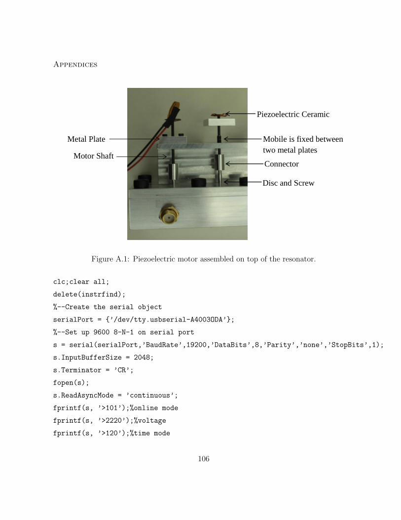
Appendices
Mobile is fixed between
two metal plates
Piezoelectric Ceramic
ceramic
Connector
Disc and Screw
Metal Plate
Motor Shaft
Figure A.1: Piezoelectric motor assembled on top of the resonator.
clc;clear all;
delete(instrfind);
%--Create the serial object
serialPort = ’/dev/tty.usbserial-A4003ODA’;
%--Set up 9600 8-N-1 on serial port
s = serial(serialPort,’BaudRate’,19200,’DataBits’,8,’Parity’,’none’,’StopBits’,1);
s.InputBufferSize = 2048;
s.Terminator = ’CR’;
fopen(s);
s.ReadAsyncMode = ’continuous’;
fprintf(s, ’>101’);%online mode
fprintf(s, ’>2220’);%voltage
fprintf(s, ’>120’);%time mode
106

Appendices
fprintf(s, ’>2059000’);%frequency (hz)
fprintf(s, ’>2128’);%duty cycle (%)
%fprintf (s, ’>3029’);
for i=1:8
fprintf (s, ’>313.2’);%move up
pause(1);
end
for i=1:1
fprintf (s, ’>323.2’);%move down
end
fprintf (s, ’>100’); %manual mode
fclose(s);
delete(s);
107


Bibliography
[1] H. Fengxi, High Q tunable filters. PhD thesis, University of Waterloo, 2012.
[2] R. Mansour, F. Huang, S. Fouladi, W. Yan, and M. Nasr, “High-q tunable filters:
Challenges and potential,” Microwave Magazine, IEEE, vol. 15, no. 5, pp. 70–82,
2014.
[3] R. J. Cameron, C. M. Kudsia, and R. R. Mansour, Microwave filters for communica-
tion systems. Wiley-Interscience, 2007.
[4] S. Fouladi, F. Huang, W. D. Yan, and R. Mansour, “Combline tunable bandpass filter
using rf-mems switched capacitor bank,” in Microwave Symposium Digest (MTT),
2012 IEEE MTT-S International, pp. 1–3, IEEE, 2012.
[5] J. Uher and W. J. Hoefer, “Tunable microwave and millimeter-wave band-pass filters,”
Microwave Theory and Techniques, IEEE Transactions on, vol. 39, no. 4, pp. 643–653,
1991.
[6] T. Shen, K. A. Zaki, and C. Wang, “Tunable dielectric resonators with dielectric
tuning disks,” Microwave Theory and Techniques, IEEE Transactions on, vol. 48,
no. 12, pp. 2439–2445, 2000.
[7] S. Fouladi, F. Huang, W. D. Yan, and R. R. Mansour, “High-narrowband tunable
combline bandpass filters using mems capacitor banks and piezomotors,” Microwave
Theory and Techniques, IEEE Transactions on, vol. 61, no. 1, pp. 393–402, 2013.
109

Bibliography
[8] M.Iskander, M. Nasr, and R. R. Mansour, “High-q tunable combline bandpass filter
using angular tuning technique,.” in Proc.European Microwave Symp. 201, to be
published.
[9] J. Krupka, A. Abramowicz, and K. Derzakowski, “Magnetically tunable filters for
cellular communication terminals,” Microwave Theory and Techniques, IEEE Trans-
actions on, vol. 54, no. 6, pp. 2329–2335, 2006.
[10] B.-W. Kim and S.-W. Yun, “Varactor-tuned combline bandpass filter using step-
impedance microstrip lines,” Microwave Theory and Techniques, IEEE Transactions
on, vol. 52, no. 4, pp. 1279–1283, 2004.
[11] L. Dussopt and G. M. Rebeiz, “Intermodulation distortion and power handling in rf
mems switches, varactors, and tunable filters,” Microwave Theory and Techniques,
IEEE Transactions on, vol. 51, no. 4, pp. 1247–1256, 2003.
[12] S.-J. Park, K.-Y. Lee, and G. M. Rebeiz, “Low-loss 5.15&# 8211; 5.70-ghz rf mems
switchable filter for wireless lan applications,” Microwave Theory and Techniques,
IEEE Transactions on, vol. 54, no. 11, pp. 3931–3939, 2006.
[13] A. Abbaspour-Tamijani, L. Dussopt, and G. M. Rebeiz, “Miniature and tunable filters
using mems capacitors,” Microwave Theory and Techniques, IEEE Transactions on,
vol. 51, no. 7, pp. 1878–1885, 2003.
[14] D. Peroulis, S. Pacheco, K. Sarabandi, and L. P. Katehi, “Tunable lumped components
with applications to reconfigurable mems filters,” in Microwave Symposium Digest,
2001 IEEE MTT-S International, vol. 1, pp. 341–344, IEEE, 2001.
[15] I. Hunter and J. D. Rhodes, “Electronically tunable microwave bandpass filters,”
Microwave Theory and Techniques, IEEE Transactions on, vol. 30, no. 9, pp. 1354–
1360, 1982.
110

References
[16] S.-J. Park and G. M. Rebeiz, “Low-loss two-pole tunable filters with three differ-
ent predefined bandwidth characteristics,” Microwave Theory and Techniques, IEEE
Transactions on, vol. 56, no. 5, pp. 1137–1148, 2008.
[17] G. L. Matthaei, “Narrow-band, fixed-tuned, and tunable bandpass filters with zig-zag
hairpin-comb resonators,” Microwave Theory and Techniques, IEEE Transactions on,
vol. 51, no. 4, pp. 1214–1219, 2003.
[18] G. Tsuzuki, M. Hernandez, E. M. Prophet, S. Jimenez, and B. A. Willemsen, “Ultra-
selective constant-bandwidth electromechanically tunable hts filters,” in 2006 IEEE
MTT-S Int. Symp. Dig., San Francisco, CA, pp. 693–696, 2006.
[19] H. Joshi, H. H. Sigmarsson, S. Moon, D. Peroulis, and W. J. Chappell, “High-fully
reconfigurable tunable bandpass filters,” Microwave Theory and Techniques, IEEE
Transactions on, vol. 57, no. 12, pp. 3525–3533, 2009.
[20] B. Yassini, M. Yu, D. Smith, and S. Kellett, “A-band high-tunable filter with stable
tuning response,” Microwave Theory and Techniques, IEEE Transactions on, vol. 57,
no. 12, pp. 2948–2957, 2009.
[21] C.-C. Cheng and G. M. Rebeiz, “High-4–6-ghz suspended stripline rf mems tunable
filter with bandwidth control,” Microwave Theory and Techniques, IEEE Transactions
on, vol. 59, no. 10, pp. 2469–2476, 2011.
[22] I. Reines, A. Brown, M. El-Tanani, A. Grichener, and G. Rebeiz, “1.6-2.4 ghz rf
mems tunable 3-pole suspended combline filter,” in Microwave Symposium Digest,
2008 IEEE MTT-S International, pp. 133–136, IEEE, 2008.
[23] A. Abunjaileh and I. Hunter, “Combline filter with tunable bandwidth and centre fre-
quency,” in Microwave Symposium Digest (MTT), 2010 IEEE MTT-S International,
pp. 1476–1479, IEEE, 2010.
111

Bibliography
[24] B. Yassini, M. Yu, and B. Keats, “A Ka-band fully tunable cavity filter,” Microwave
Theory and Techniques, IEEE Transactions on, vol. 60, no. 12, pp. 4002–4012, 2012.
[25] J. Rhodes and R. Levy, “A generalized multiplexer theory,” Microwave Theory and
Techniques, IEEE Transactions on, vol. 27, no. 2, pp. 99–111, 1979.
[26] C. Kudsia, R. Cameron, and T. WAI-CHEUNG, “Innovations in microwave filters and
multiplexing networks for communications satellite systems,” IEEE transactions on
microwave theory and techniques, vol. 40, no. 6, pp. 1133–1149, 1992.
[27] M. Guglielmi, “Simple cad procedure for microwave filters and multiplexers,” Mi-
crowave Theory and Techniques, IEEE Transactions on, vol. 42, no. 7, pp. 1347–1352,
1994.
[28] K. Saitou and K. Kageyama, “Tunable duplexer having multilayer structure using
ltcc,” in Microwave Symposium Digest, 2003 IEEE MTT-S International, vol. 3,
pp. 1763–1766, IEEE, 2003.
[29] T. Yang and G. M. Rebeiz, “Three-pole 1.3–2.4-ghz diplexer and 1.1–2.45-ghz dual-
band filter with common resonator topology and flexible tuning capabilities,” 2013.
[30] C.-F. Chen, C.-Y. Lin, B.-H. Tseng, and S.-F. Chang, “A compact tunable microstrip
diplexer using varactor-tuned dual-mode stub-loaded resonators,” in Microwave Sym-
posium (IMS), 2014 IEEE MTT-S International, pp. 1–3, IEEE, 2014.
[31] R. Kihlen, “Stripline triplexer for use in narrow-bandwidth multichannel filters,” 1972.
[32] T. Ohno, K. Wada, and O. Hashimoto, “A class of a planar triplexer by manipulating
multiple attenuation poles,” in Microwave Conference, 2004. 34th European, vol. 2,
pp. 625–628, IEEE, 2004.
[33] H. Joshi, H. H. Sigmarsson, S. Moon, D. Peroulis, and W. J. Chappell, “Tunable high
q narrow-band triplexer,” in Microwave Symposium Digest, 2009. MTT’09. IEEE
MTT-S International, pp. 1477–1480, IEEE, 2009.
112

References
[34] P. Laforge, Tunable Superconducting Microwave Filters. PhD thesis, University of
Waterloo, 2010.
[35] F. Huang, S. Fouladi, M. Nasr, and R. R. Mansour, “Three dimensional tunable filters
with absolute constant bandwidth.” Patent Pending.
[36] J. W. Bandler, R. Biernacki, S. H. Chen, R. H. Hemmers, and K. Madsen, “Electro-
magnetic optimization exploiting aggressive space mapping,” Microwave Theory and
Techniques, IEEE Transactions on, vol. 43, no. 12, pp. 2874–2882, 1995.
[37] J. W. Bandler, R. Biernacki, S. H. Chen, and Y. F. Huang, “Design optimization
of interdigital filters using aggressive space mapping and decomposition,” Microwave
Theory and Techniques, IEEE Transactions on, vol. 45, no. 5, pp. 761–769, 1997.
[38] F. C. Chen, Q. X. Chu, and J. S. Yang, “An improved group-delay approach to the
tuning of coupled-resonators fiilter,” in Microwave and Millimeter Wave Technology,
2007. ICMMT’07. International Conference on, pp. 1–4, IEEE, 2007.
[39] J. B. Ness, “A unified approach to the design, measurement, and tuning of coupled-
resonator filters,” Microwave Theory and Techniques, IEEE Transactions on, vol. 46,
no. 4, pp. 343–351, 1998.
[40] H.-P. Ko, S. Kim, S. N. Borodinas, P. E. Vasiljev, C.-Y. Kang, and S.-J. Yoon, “A
novel tiny ultrasonic linear motor using the radial mode of a bimorph,” Sensors and
Actuators A: physical, vol. 125, no. 2, pp. 477–481, 2006.
[41] H.-P. Ko, C.-Y. Kang, J.-S. Kim, S. N. Borodin, S. Kim, and S.-J. Yoon, “Con-
structions and characteristics of a tiny piezoelectric linear motor using radial mode
vibrations,” Journal of electroceramics, vol. 17, no. 2-4, pp. 603–608, 2006.
[42] R. Snyder, “Coupling probe having an adjustable tuning conductor,” Aug. 2 2005. US
Patent 6,924,718.
113

Bibliography
[43] M. Sanchez-Renedo, R. Gomez-Garcıa, J. I. Alonso, and C. Briso-Rodrıguez, “Tunable
combline filter with continuous control of center frequency and bandwidth,” Microwave
Theory and Techniques, IEEE Transactions on, vol. 53, no. 1, pp. 191–199, 2005.
[44] R. Gomez-Garcıa, M. Sanchez-Soriano, K. Tam, and Q. Xue, “Flexible filters:
Reconfigurable-bandwidth bandpass planar filters with ultralarge tuning ratio,” Mi-
crowave Magazine, IEEE, vol. 15, no. 5, pp. 43–54, 2014.
[45] G. Chaudhary, Y. Jeong, and J. Lim, “Dual-band bandpass filter with independently
tunable center frequencies and bandwidths,” Microwave Theory and Techniques, IEEE
Transactions on, vol. 61, no. 1, pp. 107–116, 2013.
[46] J. B. Thomas, “Cross-coupling in coaxial cavity filters-a tutorial overview,” Microwave
Theory and Techniques, IEEE Transactions on, vol. 51, no. 4, pp. 1368–1376, 2003.
[47] M. El Sabbagh, K. A. Zaki, H.-W. Yao, and M. Yu, “Full-wave analysis of coupling
between combline resonators and its application to combline filters with canonical
configurations,” Microwave Theory and Techniques, IEEE Transactions on, vol. 49,
no. 12, pp. 2384–2393, 2001.
[48] R. J. Cameron, A. Harish, and C. J. Radcliffe, “Synthesis of advanced microwave
filters without diagonal cross-couplings,” Microwave Theory and Techniques, IEEE
Transactions on, vol. 50, no. 12, pp. 2862–2872, 2002.
[49] R. J. Cameron and M. Yu, “Design of manifold-coupled multiplexers,” Microwave
Magazine, IEEE, vol. 8, no. 5, pp. 46–59, 2007.
114