resonant frequency and bandwidth of metamaterial emitters ... et al. 2014 jqsrt rlc.pdf · resonant...
TRANSCRIPT
Contents lists available at ScienceDirect
Journal of Quantitative Spectroscopy &Radiative Transfer
Journal of Quantitative Spectroscopy & Radiative Transfer 149 (2014) 33–40
http://d0022-40
n CorrE-m
journal homepage: www.elsevier.com/locate/jqsrt
Resonant frequency and bandwidth of metamaterial emittersand absorbers predicted by an RLC circuit model
Atsushi Sakurai a,b, Bo Zhao a, Zhuomin M. Zhang a,n
a George W. Woodruff School of Mechanical Engineering, Georgia Institute of Technology, Atlanta, GA 30332, USAb Department of Mechanical and Production Engineering, Niigata University, 8050, Ikarashi 2-no-cho, Niigata 950-2181, Japan
a r t i c l e i n f o
Article history:Received 16 April 2014Received in revised form19 July 2014Accepted 25 July 2014Available online 8 August 2014
Keywords:MetamaterialsMagnetic polaritonsRLC circuit modelSelective absorbersThermal emitters
x.doi.org/10.1016/j.jqsrt.2014.07.02473/& 2014 Elsevier Ltd. All rights reserved.
esponding author.ail address: [email protected]
a b s t r a c t
Metamaterial thermal emitters and absorbers have been widely studied for differentgeometric patterns by exciting a variety of electromagnetic resonances. A resistor–inductor–capacitor (RLC) circuit model is developed to describe the magnetic resonances(i.e. magnetic polaritons) inside the structures. The RLC circuit model allows theprediction of not only the resonance frequency, but also the full width at half maximumand quality factor for various geometric patterns. The parameters predicted by the RLCmodel are compared with the finite-difference time-domain simulation. The magneticfield distribution and the power dissipation density profile are also used to justify the RLCcircuit model. The geometric effects on the resonance characteristics are elucidated in thewire (or strip), cross, and square patterned metamaterial in the infrared region. This studywill facilitate the design of metamaterial absorbers and emitters based on magneticpolaritons.
& 2014 Elsevier Ltd. All rights reserved.
1. Introduction
Micro/nanostructured materials have drawn greatattention due to their potential applications [1–3], suchas thermophotovoltaic emitters [4,5], selective solar absor-bers [6,7], and biological sensors [8]. Most electromagneticmetamaterials consist of periodic nano/microstructuresthat exhibit exotic characteristics by excitation of reso-nances [9]. These phenomena are usually impossible torealize with naturally existing materials [10]. Metamater-ials have a great potential as perfect emitters or absorbersof thermal radiation at certain spectral bands. Landy et al.[11] experimentally demonstrated selective absorption inthe infrared region with a metallic pattern and a bottommetallic film separated by a dielectric spacer. Morerecently, various types of metamaterial structures with
(Z.M. Zhang).
different top patterns have been proposed and fabricatedas wavelength-selective emitters and absorbers. Strongconfinement of the electromagnetic energy could beachieved between the metallic pattern and the film dueto electric and magnetic resonances. Liu et al. [12] demon-strated nearly perfect absorption at the wavelength of6 μm by a cross-patterned metamaterial. Aydin et al. [13]developed an ultrathin plasmonic absorber with a nanos-tructured top silver film composed of crossed trapezoidalarrays in the visible spectrum.
Absorption and emission characteristics of metamaterials,such as the resonant frequency, strongly depend on thegeometric shape and size of the top metallic patterns. Wangand Zhang [14] numerically showed that high-performanceselective thermophotovoltaic emitter could be achieved witha metal film-coupled 1D tungsten grating structure. Theyalso experimentally studied the selective mid-infraredabsorption behavior of a film-coupled 1D gold gratingstructure [15]. Zhao et al. [16] proposed a selective thermo-photovoltaic emitter made of a film-coupled 2D tungsten

A. Sakurai et al. / Journal of Quantitative Spectroscopy & Radiative Transfer 149 (2014) 33–4034
square pattern, which exhibits strong wavelength selectivityas well as angular and polarization independence. Wang andWang [17] investigated a broadband perfect selective meta-material solar absorber made of 2D double-sized metamater-ial absorbers. Bouchon et al. [18] and Hendrickson et al. [19]experimentally demonstrated broadband absorption of meta-material absorbers with differently sized square patterns.
A simple analytical method to predict the resonanceconditions is desired for the design of single-, dual-, andmulti-band metamaterial absorbers and emitters made offilm-coupled metallic patterns. Different theories have beenproposed, such as the transmission line theory [20], inter-ference theory [21], and coupled mode theory [22]. Thepredictions of these theories show good agreement withsimulation and/or experiments for specific structures. How-ever, an easy to apply and general approach is still lacking.Since antiparallel currents can occur in the top metallicstructure and bottom metallic film under an incident time-varying magnetic field [16], magnetic polaritons (MPs) can bea plausible explanation for the resonances in those structures.An LC (inductor–capacitor) circuit model [23,24] has beensuccessfully applied to predict the resonance frequency. Inaddition to the resonance frequency, the bandwidth of theabsorption (or emission) peak is also important for the designof metamaterial absorbers (or emitters).
In the present work, an RLC (resistor–inductor–capaci-tor) circuit model is developed in order to predict theresonance characteristics, such as the frequency, full widthat half maximum (FWHM), and quality factor (Q).Although RLC circuit models have been applied to meta-materials consisting of pairs of parallel slabs and fishnetstructures [25–27], the present study focuses on theresonance conditions for metamaterial absorbers andemitters with different shapes of top metallic pattern overa bottom metallic film. The applicability of the RLC circuitmodel is explored for various geometric patterns bycomparison with the finite-difference time-domain (FDTD)simulation. Geometric effects on the resonance character-istics for metamaterials with the wire (or strip), cross, andsquare patterns are investigated in the infrared region. Thephysical mechanisms for the enhanced selective absorp-tion and emission are discussed, and the behaviors of MPsare elucidated with the magnetic field distribution, powerdissipation profile, and the RLC circuit model.
2. Geometric effects on the resonance frequency andbandwidth
Two types of patterns are considered to elucidate themechanisms for the enhanced absorption and emissionand the geometric effect. The structure contains a 2Dperiodic metal pattern over a dielectric film which isplaced atop of a metal film. The bottom metal film isopaque to infrared radiation and can easily be fabricatedon a suitable substrate. The structure without the sub-strate is illustrated in Fig. 1, with different top metallicstructures made of wire (or strip), cross, or square pat-terns. The parameters of the metamaterial structures usedin the simulations are listed in Table 1. The period of theunit cell is Λ¼3.2 μm in both the x and y directions foreach case, and the thickness of the dielectric spacer is fixed
to d¼140 nm. The patterned Au structures are located atthe center of the unit cell and Al2O3 film is used as thedielectric spacer. The geometries of the patterned struc-tures are described by the characteristic length, which isthe width w¼1.7 μm, and thickness h¼100 nm. The wirepattern can be gradually transformed to the square patternwith increasing y-directional length l. Thus, a parametersweep of l from 0.3 μm to 1.7 μm will be conducted toshow the geometric effects on the MPs in the wirepatterned structure. When the side length l of the twowires in the cross pattern are simultaneously varied from0.3 μm to 1.7 μm, the cross pattern can also be trans-formed to the square pattern. Some geometric effects onthe resonance frequency of these patterns have beeninvestigated in the previous studies [11–19,24]. Althoughthe aforementioned designs exhibit excellent absorptionand emission efficiencies, previous studies have exploredfor specific structures only without considering the effectof the y-dimensional length on the resonance frequencyand bandwidth. Therefore, how to explain the effect of l onthe resonant frequency and bandwidth quantitatively isthe interest of the present study.
The full-wave simulation based on Lumerical FDTDsoftware is used to demonstrate the geometric effects.Periodic boundary conditions are used along the x and ydirections. Perfectly-matched-layers boundary conditionsare applied along the propagation direction of electro-magnetic waves (the z direction). A broadband linearlypolarized plane wave is incident to the unit cell fromabove the structure. A frequency-domain power monitor isplaced above the plane wave source to collect the reflectedwaves. Only the transverse magnetic (TM) wave is simu-lated for which MPs can be excited by the y component ofthe magnetic field. Since the considered patterns aresymmetric, the reflectance would be the same for bothtransverse electric (TE) and TM waves. The spectral-directional emittance is equal to the spectral-directionalabsorptance according to Kirchhoff's law [10], which is oneminus the reflectance providing that the bottom metallicfilm is opaque. The normal specular reflectance is simu-lated from the FDTD, and the surface roughness effect isneglected in the simulation. The dependence of emittanceon incident angles is expected to be insignificant becausethe y component of the magnetic field, which excites themagnetic resonance, does not change when the incidenceangle changes [14,16]. All the simulations in this paper areperformed in three-dimensional computational domainusing non-uniform structured mesh with a minimummesh size of 1 nm. Alumina (Al2O3) is chosen for adielectric spacer and gold is chosen as metallic topping.The dielectric functions of alumina and gold are obtainedwith the tabulated data from Palik [28]. Here, the refrac-tive index of alumina is assumed to be constant as n¼1.57.
Fig. 2 indicates how the normal emittance changeswith the length l in the spectral region from 30 THz to60 THz (corresponding to wavelength λ from 10 μm to5 μm). When the length l changes from 0.3 μm to 1.7 μm,the normal emittance is significantly enhanced, and theresonant peak shifts to lower frequency with larger lengthl for both cases. The resonance frequencies of the crosspattern are slightly higher than that of the wire pattern

Fig. 1. Schematic of the metamaterial structure as a wavelength-selective infrared emitter or absorber. (a) The x–z plane at y¼0 nm, and top view of the x–y plane of the (b) wire, (c) cross, and (d) square pattern. Unit cells are shown that include the top metal (Au) pattern over a bottom metal film, separated bya dielectric spacer (Al2O3).
Table 1Geometric parameters for the metamaterial structure used in thepresent study.
Period Λ [μm] 3.2Thickness of top metallic pattern h [nm] 100Thickness of dielectric spacer d [nm] 140Characteristic length (width) w [μm] 1.7y-Directional length (wire) l [μm] 0.3–1.7y-Directional length (cross) l [μm] 0.3–1.7
A. Sakurai et al. / Journal of Quantitative Spectroscopy & Radiative Transfer 149 (2014) 33–40 35
when the length l is from 0.3 μm to 1.5 μm. At l¼1.7 μm,the spectra overlap because both the wire and crosspatterns transform to the square pattern. Also, the band-widths of the resonance peaks become broader withincreasing lengths l for both patterns. These resonancepeaks are originated from MPs, which are demonstratednext with a visualization of the electromagnetic fielddistribution. For this structure, surface plasmon polariton(SPP) occurs at λ¼3.2 μm (93.7 THz) at normal incidence.Moreover, higher-order MP modes and coupled modes canoccur at frequencies higher than 100 THz. Additional MPscan be excited by the strip with a length l in the x-directionfor the cross pattern and the resonance frequency is also
higher than 100 THz. The focus of the present study is thezero-order MP modes in the mid-infrared region as shownin Fig. 2.
Fig. 3 shows the electromagnetic field profile along thex–z plane at y¼0 nm at the resonant frequency ðf rÞ withdifferent geometries: (a) wire (l¼0.5 μm, f r¼47.5 THz), (b)cross (l¼0.5 μm, f r¼50.8 THz), and (c) square (l¼1.7 μm,f r¼44.3 THz) pattern, respectively. The contours show thestrength of magnetic field normalized to that of theincidence, indicating the highly localized H field enhance-ment inside the Al2O3 spacer. The arrows show the electricfield vectors, indicating the direction and strength ofinduced conduction current. A detailed analysis showsthat the full current in the structure when MPs are excitedwill always form a closed loop [16], which creates astrongly enhanced magnetic field and thus forms an MP.Fig. 4 shows the magnetic field profile when the MP isexcited of the x–y cross section at the center of dielectriclayer which is at z¼�120 nm with the same conditions asFig. 3. Clearly, there is a strong confinement of electro-magnetic energy inside the Al2O3 spacer between the topmetallic pattern and bottom film. Since the area of the linepattern is relatively small, the enhancement is stronger in

Fig. 2. Normal emittance of the metamaterial made of wire, cross, andsquare patterns with different length l. The y-axis range is from 0 to 1 inall panels.
Fig. 3. Electromagnetic field profiles at the resonant frequency along thex–z plane at y¼0 nm. The color contour shows the relative magnitude ofthe square of the y-component magnetic field. The vectors show thedirection and magnitude of the electric field: (a) wire pattern (l¼0.5 μm,f r¼47.5 THz), (b) cross pattern (l¼0.5 μm, f r¼50.8 THz), and (c) squarepattern (l¼1.7 μm, f r¼44.3 THz).
A. Sakurai et al. / Journal of Quantitative Spectroscopy & Radiative Transfer 149 (2014) 33–4036
the wire pattern metamaterial compared with the othertwo. These field patterns characterize the existence of MPs.
In previous studies, an analytical LC circuit model isemployed to explain the MPs in 1D gratings and 2Dpatches structures [16–19,29,30]. Based on the electro-magnetic field and charge distribution of the structureswhen the MPs are excited, the prediction of resonanceconditions by the LC circuit model agreed reasonably wellwith numerical simulations. In addition to the resonancewavelength, FWHMs and Q-factors are also importantdesign parameters to develop metamaterial emitters andabsorbers. The FWHM is defined as the bandwidth offrequencies on either side of a resonance curve at whichthe emission reaches half its maximum intensity. TheQ-factor equals to the resonant frequency over the band-width, and a higher Q-factor indicates stronger resonantresponse with low energy loss. An RLC circuit model isintroduced to scrutinize the resonance characteristics asdiscussed in the next section.
3. Development of the RLC circuit model
The LC circuit model has been successfully used tounderstand the physical mechanisms and the geometriceffects on MP [24]. However, the model is limited for theprediction of resonant frequency. In order to extend LCcircuit models and to explore the resonance characteris-tics, we introduce an RLC circuit model because the fieldand current configurations for the MP can be accounted forby an equivalent RLC circuit model as shown in Fig. 5. Thedifference from the parallel wire model used previously[26] is that, in the present study, the resistance and kinetic
inductance in the metal base plate are evaluated based onsheet resistance and inductance as discussed in the follow-ing. However, no distinction is given between the crosspattern and the wire pattern. The magnetic inductance ormutual inductance ðLmÞ, which is originated from themagnetic energy stored in the dielectric spacer of distanced between the two parallel wires, has the form [29]
Lm ¼ 0:5μ0wdl
ð1Þ
where μ0 is the permeability of vacuum. The (kinetic)impedance Z, which is originated from the kinetic energyof the electrons inside the metal, can be expressed as[29,30]
Z ¼ R� iωLk ð2Þwhere R and Lk are the resistance and kinetic inductance,respectively. The impedance can be evaluated by consider-ing the complex conductivity of the material and aneffective penetration depth, such that
Z ¼ wðσ0 þ iσ″ÞAeff
ð3Þ
where σ0 and σ″ are the real and imaginary parts ofcomplex conductivity, respectively, and Aeff is the effectivecross section area of the induced electric current. For thetop metallic pattern, Aeff ¼ δl and δ is an effective penetra-tion depth of the electric field. Note that the penetrationdepth of the electric field is λ=ð2πκÞ, where κ is theextinction coefficient. Although a uniform distribution of

Fig. 4. Magnetic field profiles at the resonant frequency of the x–y crosssection at the center of dielectric layer which is at z¼�120 nm. Thecontour shows the relative magnitude of the square of the y-componentmagnetic field: (a) wire pattern (l¼0.5 μm, f r¼47.5 THz), (b) crosspattern (l¼0.5 μm, f r¼50.8 THz), and (c) square pattern (l¼1.7 μm,f r¼44.3 THz).
Fig. 5. The equivalent RLC circuit model between a metal strip and thebase plate, separated by a dielectric spacer. Here, R1 and Lk1 are theresistance and kinetic inductance of the top strip, R2 and Lk2 are theresistance of the base plate, Lm is the mutual inductance, and Cm is thecapacitance between the top strip and the bottom plate.
Fig. 6. Power dissipation density profiles at the resonant frequency of thex–z cross section at y¼0 nm in the gold film: (a) wire pattern, (b) crosspattern, and (c) square pattern. The depth of x–z cross section is 30 nmbelow Al2O3/Au interface (the position of the interface is at z¼�190 nm).The geometry and resonance conditions are the same as in Fig. 4.
A. Sakurai et al. / Journal of Quantitative Spectroscopy & Radiative Transfer 149 (2014) 33–40 37
electric field is assumed in this equation, the non-uniformity of the field distribution needs to be considered.Therefore, an effective penetration depth is introduced by
using a factor c1 so that
δ¼ c1λ=ð2πκÞ ð4Þ
The distribution of power absorbed per unit volumenear the surface of metallic film is shown in Fig. 6 at theMP resonance frequency. The location at z¼�190 nmcorresponds to the Al2O3/Au interface. The power dissipa-tion density can be calculated by [31]
Pd ¼12ε0ε″ω Ej2
�� ð5Þ
The power dissipation density is related to theabsorbed power per unit volume [W/m3] or local Jouleheating. In the calculations, the magnitude of electric fieldfor the incident radiation is set to unity. The depth for the1/e decay is about 20–25 nm at resonant frequencies asshown in Figs. 6a to c. Similar distributions and decay

Fig. 7. Power dissipation density profiles at the resonant frequency of thex–y cross section at z¼�191 nm in the gold film: (a) wire pattern, (b)cross pattern, and (c) square pattern. The depth of x–y cross section is1 nm below Al2O3/Au interface. The geometry and resonance conditionsare the same as in Fig. 4.
A. Sakurai et al. / Journal of Quantitative Spectroscopy & Radiative Transfer 149 (2014) 33–4038
lengths can be obtained for the top metallic structureswhose thickness h is set to 100 nm. Note that the penetra-tion depth calculated from λ=ð2πκÞ is about 26 nm at theresonant frequency. In the present paper, c1 ¼ 2=3 is there-fore adapted in estimating the penetration depth for boththe top metal strip and the bottom metal plate. In the caseof cross, it is modeled the same as a simple strip with a y-dimensional length of l since the main interest is to studythe fundamental MP related to the width w. Using therelationship σ0 ¼ωε0ε″ and σ″¼ �ωε0ε0 [10], the resis-tance and kinetic inductance of top metallic pattern can beobtained as
R1 ¼w
ε0ωlδε″
ðε02þε″2Þ ð6Þ
Lk1 ¼ � wε0ω2lδ
ε0
ðε02þε″2Þ ð7Þ
where ε0 and ε″ are respectively the real and imaginaryparts of the complex dielectric function ε of the metalobtained from the optical constants tabulated in Palik [28].The electrons are accumulated and oscillated within thetop metallic pattern. However, the electrons are not con-fined the same way in the metallic film below thedielectric spacer. The current is allowed to flow in a widerpathway. Furthermore, the three-dimensionality of elec-tromagnetic field affects the electric charge distributionnear the surface of the metal film. Therefore, the conceptof sheet resistance or impedance is employed by assumingthat the induced electric current flow is along a squareplate. Therefore the resistance and kinetic inductance inthe metal film can be obtained by setting l¼w in Eqs. (6)and (7), resulting in
R2 ¼1
ε0ωδε″
ðε02þε″2Þ ð8Þ
Lk2 ¼ � 1ε0ω2δ
ε0
ðε02þε″2Þ ð9Þ
In order to check the square sheet approximation, thepower dissipation density is visualized at the x–y crosssection in the metal film, as shown in Fig. 7, where thedepth of cross section is 1 nm below Al2O3/Au interface(z¼�191 nm). In Fig. 7a and b, the power dissipationprofiles are broadly affected in the bottom metallic filmcompared to the top metallic patterns. For electric currentsin the wire and cross patterns, they are obviously confinedinside the top metallic strips as Fig. 4 shows. In the metalfilm, however, the electric currents may flow through amuch wider breadth than the top pattern. Therefore, thesquare sheet approximation may better describe the cur-rent flow, although it is still a simplified approximation.
The dielectric spacer separating top metal pattern andthe bottommetal film serves as a capacitor on each side, asshown in Figs. 3 and 4. The parallel-plate capacitance isexpressed as
Cm ¼ c2εdε0wld
ð10Þ
where c2 ¼ 0:2 is a numerical factor to consider the fringeeffect or non-uniform charge distribution along the sur-faces of capacitor. The capacitance between neighbor
patterns is not included since it is negligible small com-pared with Cm [14]. The total impedance of RLC circuitmodel can be obtained as follows:
ZtotðωÞ ¼ R1þR2þ2
iωCmþ iωðLk1þLk2Þþ2iωLm ð11Þ
Note that the penetration depth and dielectric functionare wavelength-dependent. The resonance conditions forthe fundamental MP mode can be obtained by zeroing thetotal impedance. The resonant frequency f r, Q-factor Q,FWHM Δf of the circuit model can be expressed as [32]
f r ¼12π
ffiffiffiffiffiffiffiffiffiffiffiffiffiffiffiffiffiffiffiffiffiffiffiffiffiffiffiffiffiffiffiffiffiffiffiffiffiffiffiffi2
Cmð2LmþLk1þLk2Þ
sð12Þ
A. Sakurai et al. / Journal of Quantitative Spectroscopy & Radiative Transfer 149 (2014) 33–40 39
Q ¼ 2R1þR2
ffiffiffiffiffiffiffiffiffiffiffiffiffiffiffiffiffiffiffiffiffiffiffiffiffiffiffiffiffiffiffi2LmþLk1þLk2
2Cm
sð13Þ
Δf ¼ 12π
R1þR2
2LmþLk1þLk2
� �ð14Þ
This RLC circuit model is able to explain the geometriceffects on the resonances in various metamaterials, whichwill be shown in the following section.
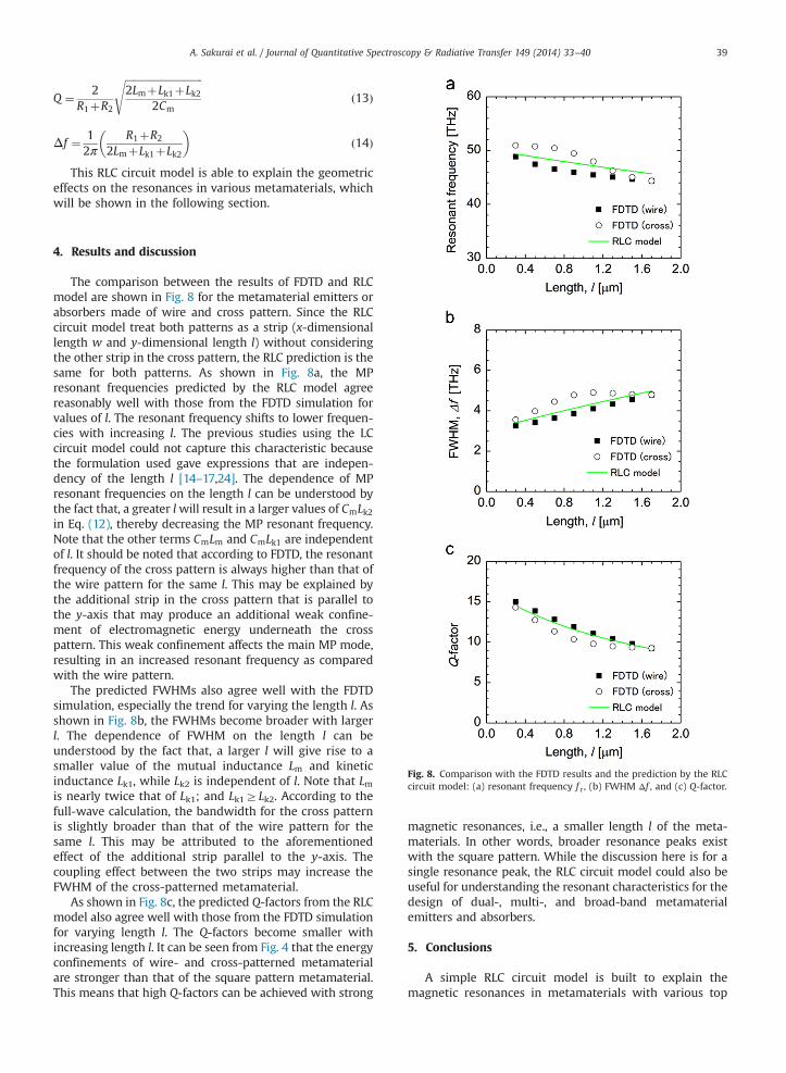
Fig. 8. Comparison with the FDTD results and the prediction by the RLCcircuit model: (a) resonant frequency f r, (b) FWHM Δf , and (c) Q-factor.
4. Results and discussion
The comparison between the results of FDTD and RLCmodel are shown in Fig. 8 for the metamaterial emitters orabsorbers made of wire and cross pattern. Since the RLCcircuit model treat both patterns as a strip (x-dimensionallength w and y-dimensional length l) without consideringthe other strip in the cross pattern, the RLC prediction is thesame for both patterns. As shown in Fig. 8a, the MPresonant frequencies predicted by the RLC model agreereasonably well with those from the FDTD simulation forvalues of l. The resonant frequency shifts to lower frequen-cies with increasing l. The previous studies using the LCcircuit model could not capture this characteristic becausethe formulation used gave expressions that are indepen-dency of the length l [14–17,24]. The dependence of MPresonant frequencies on the length l can be understood bythe fact that, a greater lwill result in a larger values of CmLk2in Eq. (12), thereby decreasing the MP resonant frequency.Note that the other terms CmLm and CmLk1 are independentof l. It should be noted that according to FDTD, the resonantfrequency of the cross pattern is always higher than that ofthe wire pattern for the same l. This may be explained bythe additional strip in the cross pattern that is parallel tothe y-axis that may produce an additional weak confine-ment of electromagnetic energy underneath the crosspattern. This weak confinement affects the main MP mode,resulting in an increased resonant frequency as comparedwith the wire pattern.
The predicted FWHMs also agree well with the FDTDsimulation, especially the trend for varying the length l. Asshown in Fig. 8b, the FWHMs become broader with largerl. The dependence of FWHM on the length l can beunderstood by the fact that, a larger l will give rise to asmaller value of the mutual inductance Lm and kineticinductance Lk1, while Lk2 is independent of l. Note that Lmis nearly twice that of Lk1; and Lk1ZLk2. According to thefull-wave calculation, the bandwidth for the cross patternis slightly broader than that of the wire pattern for thesame l. This may be attributed to the aforementionedeffect of the additional strip parallel to the y-axis. Thecoupling effect between the two strips may increase theFWHM of the cross-patterned metamaterial.
As shown in Fig. 8c, the predicted Q-factors from the RLCmodel also agree well with those from the FDTD simulationfor varying length l. The Q-factors become smaller withincreasing length l. It can be seen from Fig. 4 that the energyconfinements of wire- and cross-patterned metamaterialare stronger than that of the square pattern metamaterial.This means that high Q-factors can be achieved with strong
magnetic resonances, i.e., a smaller length l of the meta-materials. In other words, broader resonance peaks existwith the square pattern. While the discussion here is for asingle resonance peak, the RLC circuit model could also beuseful for understanding the resonant characteristics for thedesign of dual-, multi-, and broad-band metamaterialemitters and absorbers.
5. Conclusions
A simple RLC circuit model is built to explain themagnetic resonances in metamaterials with various top

A. Sakurai et al. / Journal of Quantitative Spectroscopy & Radiative Transfer 149 (2014) 33–4040
metallic pattern length in the y-dimension. The mainfeature is to treat the resistance and kinetic inductanceof the top patterned structure and the bottom filmdifferently considering the field distributions. The pre-dicted results are compared with that of FDTD simulationand good agreement in the predicted trends is obtained.As an extension of the LC circuit model, the modified RLCcircuit model can reasonably predict the resonant char-acteristics such as resonant frequency, FWHM, andQ-factor of the MP resonant peaks. This study will benefitthe understanding of magnetic resonances in metamater-ial structures and facilitate the design of metamaterialabsorbers and emitters.
Acknowledgments
This work was supported by the National ScienceFoundation (CBET-1235975). The authors would like tothank Dr. Junming Zhao of Harbin Institute of Technologyfor valuable comments.
References
[1] Fu CJ, Zhang ZM. Thermal radiative properties of metamaterials andother nanostructured materials: a review. Front Energy Power EngChina 2009;3:11–26.
[2] Zhang ZM, Wang LP. Measurements and modeling of the spectraland directional radiative properties of micro/nanostructured mate-rials. Int J Thermophys 2013;34:2209–42.
[3] Watts CM, Liu XL, Padilla WJ. Metamaterial electromagnetic waveabsorbers. Adv Mater 2012;24:OP98–120.
[4] Maruyama S, Kashiwa T, Yugami H, Esashi M. Thermal radiationfrom two-dimensionally confined modes in microcavities. Appl PhysLett 2001;79:1393–5.
[5] Bermel P, Ghebrebrhan M, Chan W, Yeng YX, Araghchini M, HamamR, et al. Design and global optimization of high-efficiency thermo-photovoltaic systems. Opt Express 2010;18:A314–34.
[6] Sergeant NP, Agrawal M, Peumans P. High performance solar-selective absorbers using coated sub-wavelength gratings. OptExpress 2010;18:5525–40.
[7] Sakurai A, Tanikawa H, Yamada M. Computational design for a wide-angle cermet-based solar selective absorber for high temperatureapplications. J Quant Spectrosc Radiat Transf 2014;132:80–9.
[8] Liu N, Mesch M, Weiss T, Hentschel M, Giessen H. Infrared perfectabsorber and its application as plasmonic sensor. Nano Lett 2010;10:2342–8.
[9] Pendry JB, Holden AJ, Robbins DJ, Stewart WJ. Magnetism fromconductors and enhanced nonlinear phenomena. IEEE Trans MicrowTheory Tech 1999;47:2075–84.
[10] Zhang ZM. Nano/microscale heat transfer. New York: McGraw-Hill;2007.
[11] Landy NI, Sajuyigbe S, Mock JJ, Smith DR, Padilla WJ. Perfectmetamaterial absorber. Phys Rev Lett 2008;100:207402.
[12] Liu XL, Tyler T, Starr T, Starr AF, Jokerst NM, Padilla WJ. Taming theblackbody with infrared metamaterials as selective thermal emit-ters. Phys Rev Lett 2011;107:045901.
[13] Aydin K, Ferry VE, Briggs RM, Atwater HA. Broadband polarization-independent resonant light absorption using ultrathin plasmonicsuper absorbers. Nat Commun 2011;2:517.
[14] Wang LP, Zhang ZM. Wavelength-selective and diffuse emitterenhanced by magnetic polaritons for thermophotovoltaics. ApplPhys Lett 2012;100:063902.
[15] Wang LP, Zhang ZM. Measurement of coherent thermal emissiondue to magnetic polaritons in subwavelength microstructures. J HeatTransf 2013;135:091505.
[16] Zhao B, Wang LP, Shuai Y, Zhang ZM. Thermophotovoltaic emittersbased on a two-dimensional grating/thin-film nanostructure. Int JHeat Mass Transf 2013;67:637–45.
[17] Wang H, Wang LP. Perfect selective metamaterial solar absorbers.Opt Express 2013;21:A1078–93.
[18] Bouchon P, Koechlin C, Pardo F, Haidar R, Pelouard JL. Widebandomnidirectional infrared absorber with a patchwork of plasmonicnanoantennas. Opt Lett 2012;37:1038–40.
[19] Hendrickson J, Guo JP, Zhang BY, Buchwald W, Soref R. Widebandperfect light absorber at midwave infrared using multiplexed metalstructures. Opt Lett 2012;37:371–3.
[20] Engheta N. Circuits with light at nanoscales: optical nanocircuitsinspired by metamaterials. Science 2007;317:1698–702.
[21] Chen H-T. Interference theory of metamaterial perfect absorbers.Opt Express 2012;20:7165–72.
[22] Zhu L, Sandhu S, Otey C, Fan SH, Sinclair MB, Luk TS. Temporalcoupled mode theory for thermal emission from a single thermalemitter supporting either a single mode or an orthogonal set ofmodes. Appl Phys Lett 2013;102:103104.
[23] Zhou J, Economon EN, Koschny T, Soukoulis CM. Unifying approachto left-handed material design. Opt Lett 2006;31:3620–2.
[24] Sakurai A, Zhao B, Zhang ZM. Prediction of the resonance conditionof metamaterial emitters and absorbers using LC circuit model. In:Proceedings of 15th international heat transfer conference, 2014,IHTC15-9012, 1-10.
[25] Fu L, Schweizer H, Guo H, Liu N, Giessen H. Synthesis of transmis-sion line models for metamaterial slabs at optical frequencies. PhysRev B 2008;78:115110.
[26] Zhou J, Koschny T, Soukoulis CM. An efficient way to reduce losses ofleft-handed metamaterials. Opt Express 2008;16:11147–52.
[27] Penciu RS, Kafesaki M, Koschny T, Economou EN, Soukoulis CM.Magnetic response of nanoscale left-handed metamaterials. PhysRev B 2010;81:235111.
[28] Palik ED. Handbook of optical constants of solids. San Diego:Academic Press; 1998.
[29] Wang LP, Zhang ZM. Phonon-mediated magnetic polaritons in theinfrared region. Opt Express 2011;19:A126–35.
[30] Zhao B, Zhang ZM. Study of magnetic polaritons in deep gratings forthermal emission control. J Quant Spectrosc Radiat Transf 2014;135:81–9.
[31] Hao J, Zhou L, Qiu M. Nearly total absorption of light and heatgeneration by plasmonic metamaterials. Phys Rev B 2011;83:165107.
[32] Solymar L, Shamonina E. Waves in metamaterials. Oxford: OxfordUniversity Press; 2009.