design multiband e-shaped fractal microstrip …eprints.utem.edu.my/18296/1/design multiband...
TRANSCRIPT

DESIGN MULTIBAND E-SHAPED FRACTAL MICROSTRIP PATCH
ANTENNA WITH DEFECT GROUND STRUCTURE (DGS) BY USING
GRAPHENE
MOHD NURUL ANUAR BIN FALELLAH
This Report Is Submitted In Fulfilment of Requirement for the Bachelor Degree of
Electronic Engineering (Wireless Communication) With Honors
Faculty of Electronic and Computer Engineering
Universiti Teknikal Malaysia Melaka
JUN 2016

ii
UNIVERSTI TEKNIKAL MALAYSIA MELAKA FAKULTI KEJURUTERAAN ELEKTRONIK DAN KEJURUTERAAN KOMPUTER
BORANG PENGESAHAN STATUS LAPORAN
PROJEK SARJANA MUDA II
Tajuk Projek : …Design Multiband E-Shaped Fractal Microstrip Patch Antenna With Defect Ground Structure By Using Grphene
Sesi Pengajian :
111 5 5 / / 1 1 6 6
Saya MOHD NURUL ANUAR BIN FALELLAH mengaku membenarkan Laporan Projek Sarjana Muda ini disimpan di Perpustakaan dengan syarat-syarat kegunaan seperti berikut:
1. Laporan adalah hakmilik Universiti Teknikal Malaysia Melaka.
2. Perpustakaan dibenarkan membuat salinan untuk tujuan pengajian sahaja.
3. Perpustakaan dibenarkan membuat salinan laporan ini sebagai bahan pertukaran antara institusi
pengajian tinggi.
4. Sila tandakan ( √ ) :
5.
SULIT*
*(Mengandungi maklumat yang berdarjah keselamatan atau
kepentingan Malaysia seperti yang termaktub di dalam AKTA RAHSIA RASMI 1972)
TERHAD**
**(Mengandungi maklumat terhad yang telah ditentukan oleh
organisasi/badan di mana penyelidikan dijalankan)
TIDAK TERHAD
Disahkan oleh:
__ ________________________ ___________________________________ (TANDATANGAN PENULIS) (COP DAN TANDATANGAN PENYELIA)
Tarikh: ……………………….. Tarikh: ………………………..

iii
“I hereby declare that the work in this project is my own except for summaries and
quotations which have been duly acknowledged.”
Signature : .......................................................
Author : MOHD NURUL ANUAR BIN FALELLAH
Date : 20 JUNE 2016

iv
“I acknowledge that I have read this report and in my opinion this report is sufficient
in term of scope and quality for the award of Bachelor of Electronic Engineering
(Industrial Electronics/ Computer Engineering/ Electronic Telecommunication/
Wireless Communication)* with Honours.”
Signature : .......................................................
Supervisor’s Name : MR. AZMAN BIN AWANG TEH
Date : 20 JUNE 2016

v
Special dedication to my loving father, Falellah Bin Othman and my mother Siti
Rukiam Binti Karmo, thank you for all support until complete my thesis.

vi
ACKNOWLEDGMENT
Firstly, I would like to express my sincere gratitude to my advisor , En Azman Bin
Awang Teh for the continuous support of my Final Year Project study and related
research, for his patience, motivation, and immense knowledge. His guidance helped
me in all the time of research and writing of this thesis. I could not have imagined
having a better advisor and mentor for my degree study.
Besides my advisor, I would like to thank the rest of my panel for FYP1 and FYP 2:
PM Dr Zahriladha Bin Zakaria and En Fauzi Bin Hj Abdul Wahab for their
insightful comments and encouragement, but also for the hard question which
incented me to widen my research from various perspectives.
Last but not the least, I would like to thank my family: my parents and to my
brothers and sister for supporting me spiritually throughout writing this thesis and
my my life in general.

vii
ABSTRACT
To have small, compatible and affordable antennas is the need of today’s mobile
devices. Microstrip antennas are the best choice for wireless devices because of
characteristics like low weight, ease of fabrication and low cost. But on the other
hand, microstrip antenna also suffers from disadvantages like they have less
bandwidth and gain. So, measure issues for consideration are a multiband and
wideband operation of the antenna. In order to obtain multiband and wideband
characteristics, different techniques can be used such as cutting a slot in the patch,
fractal geometry and DGS (Defected Ground structure). In order to increase
bandwidth, DGS can be used. It is to be noted that within a particular area of ground
different DGS can produce different resonant frequencies and different bandwidth.
In this thesis, the use of fractal geometry with three iterations has been proposed.
This results in multiband operation of the antenna with added advantage of size
reduction. Further, the wideband characteristic of the antenna is improved by
applying DGS. Nowadays, graphene has attained a great demand from the device
community. In this project, graphene is an element that preferred in replacing the
copper as patch material to improve the performance of the antenna. This is because
of its advantages for instance light weight, strong, transparent and good conductor of
heat and electricity. From this project, the best optimization design is using the third
iteration with DGS antenna. The antenna is designed and simulated by using
Computer Simulation Studio 2011 (CST) software.By applying the concept of fractal
geometry on a rectangular patch, a self-similar E-Shaped structure has been
obtained. Also, by using FR-4 epoxy (Fire Retardant-4) as substrate antenna
resonates at 5.6GHz,7.3GHz, 8.4GHz ,and 9.6GHz respectively with bandwidth
233MHz, 462MHz, 341MHz and 396MHz at corresponding frequencies. Graphene
material shows a better performance compare to copper as the patch material in term
of return loss, bandwidth and gain have also been proved in this thesis.
viii
ABSTRAK
Antena yang kecil, sesuai dan mampu milik adalah antara ciri yang diperlukan oleh
peranti mudah alih. Mikrostrip antena adalah pilihan yang terbaik untuk peranti
tanpa wayar kerana cirinya yang ringan, mudah untuk di reka dan murah.
Walaubagaimanapun, mikrostrip antena mempunyai kekurangan seperti kurang
kelebaran jalur dan rendah gandaan. Jadi, ciri yang akan dititikberatkan adalah ciri
pelbagai jalur dan jalur lebar. Untuk mendapatkan ciri pelbagai jalur dan jalur lebar,
pelbagai teknik boleh digunakan seperti memotong slot di tampalan, fraktal geometri
dan teknik DGS (Defect Ground Structure). Untuk meningkatkan kelebaran jalur,
DGS boleh digunakan. Untuk diambil perhatian, keluasan tapak DGS yang berbeza
boleh menghasilkan pelbagai frekuensi dan kelebaran jalur. Di dalam tesis ini,
sebanyak tiga pengulangan fraktal geometri telah direka. Hal ini menghasilkan
operasi pelbagai jalur di tampalan antena dengan tambahan pengurangan saiz. Selain
itu, ciri jalur lebar unutk antenna telah ditingkatkan dengan mengunakan DGS. Pada
masa kini, graphene telah mendapat permintaan yang tinggi dalam kalangan
komuniti peranti. Dalam projek ini, unsur graphene telah dipilih untuk mengantikan
tembaga unutk meningkatkan prestasi antena. Hal ini adalah kerana, kelebihannya
seperti ringan, kuat, telus dan konduktor haba dan elektrik yang baik. Dalam projek
ini, reka bentuk optimum yang terbaik adalah antena ulangan ketiga dengan ciri
DGS. Antena ini direka dan disimulasi menggunakan perisian Computer Simulation
Studio 2011 (CST). Dengan menggunakan konsep fraktal geometri di tampalan segi
empat tepat, kesamaan sendiri bentuk E telah diperolehi. Juga dengan menggunakan
FR-4 (Fire Retardant-4) sebagai substrat antenna resonansi di 5.6GHz,7.3GHz,
8.4GHz and 9.6GHz masing-masing dengan kelebaran jalur 233MHz, 462MHz,
341MHz and 396MHz di frekuensi tersebut. Di dalam tesis ini membuktikan bahawa
unsur graphene menunjukkan prestasi yang lebih baik berbanding tembaga sebagai
patch dari segi kehilangan balik, kelebaran jalur dan gandaan.

ix
TABLE OF CONTENTS
CHAPTER SUBJECT PAGE
PROJECT TITLE i
STATUS REPORT DECLARATION FORM ii
STUDENT DECLARATION iii
DECLARATION SUPERVISOR iv
DEDICATION v
ACKNOWLEDGMENT vi
ABSTRACT vii
ABSTRAK viii
CONTENT ix
LIST OF TABLE xii
LIST OF FIGURE xiii
1 INTRODUCTION
1.1 Project Background 2
1.1.1 Graphene 2
1.2 Problem Statement 3
1.3 Objectives 4
1.4 Scope of Project 4
1.5 Brief Explanation of Methodology 5
1.6 Thesis Plan 5

x
2 LITERATURE REVIEW
2.1 Antenna definition 7
2.2 Microstrip Antenna 8
2.3 Fractal Geometry 9
2.4 Feeding technique 11
2.5 Defect Ground Structure 12
2.6 Antenna Parameter 13
2.6.1 Radiation Pattern 13
2.6.2 Directivity 14
2.6.3 Bandwidth 14
2.6.4 Gain 15
2.6.5 Polarization 15
2.6.6 Antenna efficiency 16
2.7 Graphene 16
3 METHODOLOGY
3.1 Overview of Methodology 19
3.2 Substrate Material 20
3.3 Designing Antenna 21
3.3.1 Calculation of Patch dimension 21
3.3.2 E-shaped Fractal Microstrip Antenna Design 22
3.4 Introduction to CST 2011 Studio Suite Software 26
3.5 Flowchart 27
4 RESULT AND DISCUSSION
4.1 Comparison of different iterations 28
4.1.1 First Iteration 28
4.1.1.1 Return Loss 29
4.1.1.2 Bandwidth 29

xi
4.1.1.3 Gain 30
4.1.2 Second Iteration 31
4.1.2.1 Return Loss 31
4.1.2.2 Bandwidth 32
4.1.2.3 Gain 32
4.1.3 Third Iteration 35
4.1.3.1 Return Loss 35
4.1.3.2 Bandwidth 36
4.1.3.3 Gain 37
4.2 Effect on Defected Ground Structure (DGS) on Antenna 40
4.3 Comparison for Overall Result 47
5 CONCLUSION AND RECOMMENDATION
5.1 Conclusion 50
5.2 Recommendation 51
6 REFERENCES 52

xii
LIST OF TABLES
NO TITLE PAGE
2.1 Conductivity of material 17
3.1 Parameter of substrate material 21
4.1 Bandwidth for the first iteration 29
4.2 Gain for the first iteration 30
4.3 Bandwidth for the second iteration 32
4.4 Gain for the second iteration 32
4.5 Bandwidth for the third iteration 36
4.6 Gain for the third iteration 37
4.7 Comparison table of the third iteration 41
4.8 Overall result 47

xiii
LIST OF FIGURES
NO TITLE PAGE
2.1 Electric and magnetic wave produced by RF 8
2.2 Type of patch antenna 9
2.3 (a) Fractal geometry shape: Miwonski island 10
(b) Fractal geometry shape: Koch loop 11
2.4 Feeding technique: Microstrip feed and coaxial feed 12
2.5 Example of antenna with DGS 12
2.6 Radiation pattern 14
2.7 Type of polarization 15
2.8 Reflection, conduction, and dielectric losses 16
2.9 Structure of graphene 17
3.1 Basic Rectangular Geometry Microstrip Antenna 20
3.2 Miwonski Fractal Geometry 23
3.3 Basic rectangular patch 23
3.4 First iteration of rectangular geometry 24
3.5 Second iteration of rectangular geometry 24
3.6 Third iteration of rectangular geometry 25
3.7 Dumb bell-shaped DGS 25
3.8 CST Studio Suite Software 26
3.9 Flow chart 27
4.1 Return loss for the first iteration 29
4.2 Gain for the first iteration for copper 3.4 GHz 30
4.3 Gain for the first iteration for graphene 3.4 GHz 31
4.4 Return loss for the second iteration 31
4.5 Gain for the second iteration for copper at 3.7 GHz 33

xiv
4.6 Gain for the second iteration for graphene 3.7 GHz 34
4.7 Gain for the second iteration for copper at 6.4 GHz 34
4.8 Gain for the second iteration for graphene 6.4 GHz 35
4.9 Return loss for the third iteration 35
4.10 Gain for the third iteration for copper at 5.8 GHz 37
4.11 Gain for the third iteration for graphene at 5.8 GHz 38
4.12 Gain for the third iteration for copper at 7.4 GHz 38
4.13 Gain for the third iteration for graphene at 7.4 GHz 39
4.14 Gain for the third iteration for copper at 8.2 GHz 39
4.15 Gain for the third iteration for graphene at 8.2 GHz 40
4.16 Return loss with DGS and without DGS 42
4.17 Gain for the third iteration with DGS for copper at 5.6GHz 42
4.18 Gain for the third iteration with DGS for graphene at 5.6 GHz 43
4.19 Gain for the third iteration with DGS for copper at 7.3GHz 43
4.20 Gain for the third iteration with DGS for graphene at 7.3 GHz 44
4.21 Gain for the third iteration with DGS for copper at 8.4GHz 44
4.22 Gain for the third iteration with DGS for graphene at 8.4 GHz 45
4.23 Gain for the third iteration with DGS for copper at 9.6GHz 45
4.24 Gain for the third iteration with DGS for graphene at 9.6 GHz 46

CHAPTER 1
INTRODUCTION
This chapter will explain about the background of the project. Besides, this chapter
will discuss the problem statement, objective, and scope of the project that have been
chosen to design and simulate.
An antenna is defined by Webster’s Dictionary as “a usually metallic device (as a
rod or wire) for radiating or receiving radio waves.” The IEEE Standard Definitions
of Terms for Antennas (IEEE Std 145–1983) defines the antenna or aerial as “a
means for radiating or receiving radio waves.”[1]. On the other word, the antenna is
the medium of transition between free-space and guiding device. The transmission
line such as coaxial line or waveguide is used to transport electromagnetic energy
from the source to antenna or vice versa. There are numerous sorts of the antenna,
for example, wire antennas, horn antennas, microstrip antennas, array antennas, lens
antennas. Diverse sorts of the antenna have distinctive sorts of use.
With the demand for high-performance aircraft, spacecraft, satellite, and missile
application where the size, weight and performance are limited, low profile antenna
is required. As well as wireless communications, they also want similar
specification. To meet this increasing demand, microstrip antennas can be used. By
the progression of time, microstrip antenna got to be one of the quick developing

2
sections in the business of telecom and accepted to be the indispensable and favored
medium for what's to come. Nowadays, this sort of antenna has a substantial interest
by the end client and purchaser for a coordinated remote computerized application.
1.1 Project Background
This project has been proposed to design multiband E-shaped fractal microstrip
patch antenna with Defect Ground Structure (DGS) by using Graphene. The fractal
patch design with DGS at the ground plane technique will be done and simulated by
using Computer Simulation Tool (CST) software. The property of self-similarity of
fractal geometries is used to achieve multiband operations from fractal antennas and
their space-filling property is used for the antenna miniaturization[2]. Antenna
miniaturization is an important task in achieving the optimal design for wireless
communication[3]. This design will compare the performance of the antenna by
using copper and graphene as patch material. The graphene could potentially lead to
very interesting features such as miniaturization, dynamic tuning and even optical
transparency and mechanical flexibility[4][5]. The performance of the designed
antenna was also compared with three iterations of fractal geometry in term of return
loss,bandwidth and gain. There are also some aspects need to reconsider such that
selection of resonant frequency, type of substrate, feeding technique, the thickness
and dielectric constant of the substrate to meet a good result with DGS for wireless
application by using graphene[6].
1.1.1 Graphene
During the last years, the interest in graphene experienced impressive growth due to
its extraordinary mechanical, electronic and optical properties of the latter. Graphene
is a thin layer of pure carbon; it is a single, tightly packed layer of carbon atoms that
are bonded together in a hexagonal honeycomb lattice. Graphene is so special
because of it atomic thickness. Although it is very thin but it also very strong
material.

3
It was hypothetically asserted that two-dimensional substances neglected to exist in
view of the absence of warm strength when isolated. Still, after graphene was
disconnected, clearly that it appeared to be really conceivable, and it set aside
analysts a touch of time to find the right way. After suspended graphene sheets were
dissected by transmitting electron microscopy, specialists expressed that they found
a justifiable reason of slight undulating in the graphene, modifying arrangement of
the material. Indeed, even thus, later on, exploration suggests that it is entirely due to
the carbon to carbon bonds in graphene are so reduced furthermore solid that they
maintain a strategic distance from warm changes from destabilizing it.
In general, the conductivity of graphene is very frequency-dependent, and can have
completed different behavior. Though graphene is known as best conductor known
for electric and heat. By injecting energy to graphene, the Fermi level can be shift
and modify its electrical properties. Moreover, when the Fermi-level moves into the
valence or conduction band, the hole or electron conduction begins to dominate the
current transport and hence the resistance becomes low. This energy can be provided
by an external electric field . The gate-induced carriers can be seen as resulting from
an electrical doping, analogous to the chemical doping typically used for
semiconductor devices. The huge difference is that the semiconductor doping is an
irreversible process, while the graphene electrical doping is completely reversible.
Then, in graphene, the electrons and holes are electrically induced by applying a
positive or a negative voltage with respect to a reference electrode.
Tests have demonstrated that the electronic portability of graphene is high. It is said
that graphene electrons act like photons in their portability because of their absence
of mass. Graphene likewise contains versatile properties, having the capacity to hold
its beginning size after strain. [7] [8]
1.2 Problem Statement
The microstrip antenna is preferred due to some advantages for example low weight,
low cost, ease of fabrication and versatility in terms of resonant frequency,
polarization, pattern and impedance[6][9]. However, there are some limitations in

4
microstrip antenna such that low return loss, less bandwidth and low gain[9]. These
disadvantages can be overcome by constructing fractal patch antenna with
DGS.[6][9][10]. This project also is done to improve the antenna performance by
replacing patch material of the antenna from copper to graphene. Graphene is the
best conductor known, it is mono-atomic and thus, the surface resistance is very high
compared to metals[11]. The conductivity of graphene is very frequency-dependent
and can have completed different behavior[11]. Furthermore, graphene is going
through impressive growth due to the extraordinary mechanical, electronic and
optical properties [4][8]. So, the improvement needs to be simulated by CST Studio
Suite to prove that graphene is better than copper in term of performance.
1.3 Objectives
The main objective of this project is to design multiband E-shaped fractal microstrip
patch antenna with DGS by using Graphene. The design’s performance will be more
focus on return loss, bandwidth, and gain, and will be simulated and tested by CST
Studio Suite software.
1. To design and simulate multiband E-shaped fractal microstrip patch
antenna with DGS by using CST software.
2. To evaluate the performance between the three iterations of fractal
geometry with DGS microstrip antenna.
3. To identify the performance of the Graphene replaced copper as patch
material.
1.4 Scope Project
The antenna will be applying the concept of fractal geometry which is Miwonski
shape for antenna patch. Three iterations are performed and results are compared in
terms of antenna parameters. FR4 epoxy (Fire Retardant-4) is chosen as a substrate
5
for the antenna. The designed antenna will be developed for multiband operations for
radar, satellite, and long range radio telecommunication applications . Coaxial feed
has been used as the feeding method for microstrip antenna design. The proposed
antenna will be inserted with DGS to improve various parameters such as return loss,
bandwidth, and gain. Besides, two types of patch material have been used which are
graphene and copper to identify and compare the performance.
1.5 Brief Explanations on Methodology
Numerous exploration on the task should be done to guarantee that the project
will run easily. Essential stage, need to learn hypothetically the idea of microstrip
patch antenna and graphene to actualize it in the recommended antenna. Next
step, the planning and reenactment process by utilizing the CST programming.
To wrap things up, break down the outcomes in term of performance of three
iterations of fractal geometry and comparison of graphene and copper.
1.6 Thesis Plan
Chapter 1 - In this section, quickly clarify about the introduction of the project. A
brief explanation about the definition of antenna and sorts of antenna additionally
clarified. This section additionally including the project background, problem
statement, objective, and scope of projects.
Chapter 2 - In this section, a literature review is a place the clarifications of past
research and journal that related with this task. Past research incorporated the
final results, formula and calculation of the antenna and the graphene.
Chapter 3 - Methodology is a rule to finish and runs the project easily. Begin
from the research on the related antenna and graphene with the goal that it
satisfies every one of the prerequisites so as to meet sought results.

6
Chapter 4 - In this part, it will display all the organization information and
results. As the outcomes have been organized, the investigation of information
should be possible. There will likewise discussion about the results.
Chapter 5 - There will a proposal and future work in light of this project. And in
addition, the clarification of general conclusion for the entire project.

CHAPTER 2
LITERATURE REVIEW
This chapter survey hypothetically to get a thought that related with this undertaking so it can
plans and reenact the project by utilizing a fitting idea. From the gathered data, it can be a
rule in this project to enhance the proposed project with the goal that it works effectively.
2.1 Antenna definition
Antenna is an important terminal device in all type of communication and radar system. If the
antenna is well designed it can transmit signal from one place to various place on the globe. If
the antenna is not well designed the signal is impossible to send a signal even beyond the
premises. All communication and radar system require and antenna in one form or the other.
If there is no antenna, there would be no communication and radar system. The antenna acts
as both source and sensor for electromagnetic waves. The behavior of the electromagnetic
wave is between transmitter and receiver is important because receive power depends on
propagation characteristics.[12]
An antenna is basically a transducer that converts radio frequency(RF) electric current into
electromagnetic(EM) wave at the same frequency. The antenna can produce electric and
magnetic fields that eventually produce an electromagnetic field. This field will obtain the
transmission and reception of EM energy. It forms both the transmitter and receiver circuit.
The equivalent circuit features resistance, inductance, and capacitance. The currents produce

8
the magnetic field and charge produce electrostatic field. These two in turn create induction
field. When RF is applied to the antenna both electric and magnetic field produced as shown
in figure 2.1.[12]
Figure 2.1: Electric and magnetic wave produced by RF
Moreover, getting or transmitting vitality, an antenna in a propelled remote framework is
generally required to streamline or emphasize the radiation vitality in some headings and
smother it in others. Accordingly the antenna should also serve as a directional gadget and
examine gadget. It should then take different structures to meet the specific need close by,
and it might be a bit of directing wire, an opening, a patch, array (exhibit), a reflector, a lens,
et cetera[1].
2.2 Microstrip antenna
To have small, compatible and affordable antennas is the need of today’s mobile devices.
Microstrip antennas are the best choice for wireless devices because of characteristics like
low weight, ease of fabrication and low cost [6]. The major disadvantages of the microstrip
antenna are low efficiency, low gain, poor polarization, narrow bandwidth and spurious feed
radiation [9][20]. Starting from 1970, microstrip antenna receives huge attention. Microstrip
antenna consists of a very thin metallic strip or patch above the ground plane. For a
rectangular patch, the length L of the element usually λ0/3 < L < λ0/2. The patch and ground
plane is separated by dielectric known as substrate[12].
There are various substrates that can be utilized for the configuration of microstrip antenna
also, their dielectric constants are as a rule in the scope of 2.2 ≤ Ir ≤ 12. The ones that are
9
most alluring for good antenna execution are thick substrates whose dielectric consistent is at
the lower end of the extent in light of the fact that they give better proficiency, bigger data
transfer capacity, inexactly headed fields for radiation into space, however to the detriment of
bigger component size. Slim substrates with higher dielectric constants are attractive for
microwave hardware in light of the fact that they require firmly bound fields to minimize
undesired radiation and coupling, and prompt littler component sizes; on the other hand, due
to their more noteworthy misfortunes, they are less productive and have generally littler data
transmissions. Since microstrip antenna are frequently coordinated with other microwave
hardware, a trade-off must come to between great antenna execution and circuit outline.[12]
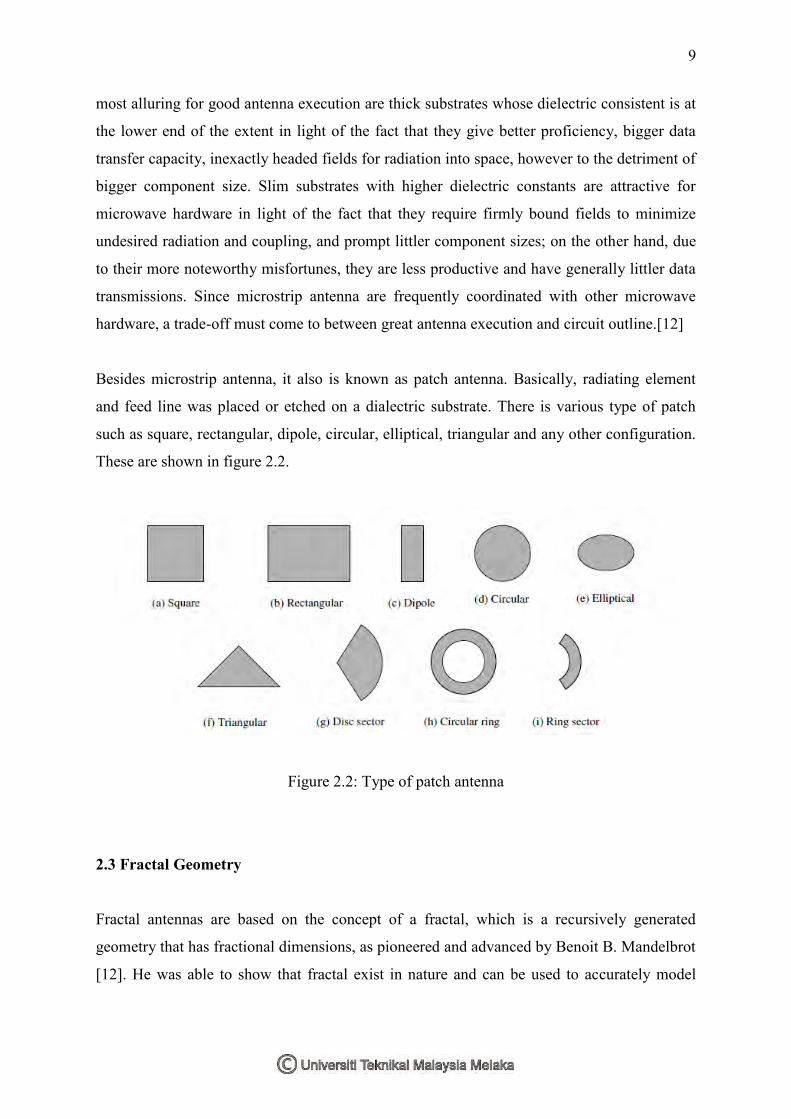
Besides microstrip antenna, it also is known as patch antenna. Basically, radiating element
and feed line was placed or etched on a dialectric substrate. There is various type of patch
such as square, rectangular, dipole, circular, elliptical, triangular and any other configuration.
These are shown in figure 2.2.
Figure 2.2: Type of patch antenna
2.3 Fractal Geometry
Fractal antennas are based on the concept of a fractal, which is a recursively generated
geometry that has fractional dimensions, as pioneered and advanced by Benoit B. Mandelbrot
[12]. He was able to show that fractal exist in nature and can be used to accurately model

10
certain phenomena. Moreover, he also introduced into a more complex structure including
trees and mountain that has self-similarity and self- affinity in their geometrical shape.
There are two categories that can describe fractal geometry which is deterministic and
random. Deterministic such as von Koch snowflake and Seiperski Gaskett are those
generated by scaled down and rotated copies. This fractal can be generated using computer
graphic by requiring particular mapping that is repeated over and over sing a recursive
algorithm. Meanwhile, random fractal can obtain through randomness over the natural
phenomenon.
Fractal geometry is used for miniaturization of the antenna which it can reduce the antenna
size[22]. There are very different from Euclidean geometry which they have two common
properties;space filling and self-similarity. The property of space filling is for size reduction
and self-similarity is to achieve multiband operation [2]. It has been shown that a limited
number of iteration of fractal geometry can make an antenna multiband. Based on their
interesting properties, there have been used in radiating systems and microwave device.
Fractal configurations iterative procedure allow them to achieve long linear dimensions and
high surface areas in limited volume.
There are a number of fractal shapes like Sipernski Gasket, Minkowski,Hilbert Curve and
Koch Curve, Fractal Arrays [6]. The example of the shape was shown in Figure 2.3(a,b).
Figure 2.3(a) exhibits what is referred to as the Minkowski island fractal, while Figure 2.3(b)
illustrates the Koch fractal loop.
Figure 2.3(a): Fractal geometry shape: Miwonski island