design of a low current leakage integrator for non ...516880/fulltext01.pdfdesign of a low current...
TRANSCRIPT

Design of a Low Current Leakage Integrator for Non-Coherent
Ultra-WideBand Receiver
By
Alper Karakuzulu
A thesis submitted to
Royal Institute of Technology for
the degree of Master Science in
System-on-Chip-Design
School of Information and Communication Technology
Royal Institute of Technology
Ipack VINN Excellence Center
February 2012
Stockholm,Sweden
TRITA-ICT-EX-2012:23
Examiner at KTH
Prof. Li-Rong Zheng
Supervisors at Ipack VINN Excellence Center and KTH
Tekn. Dr. and Vice Director of iPack VINN Excellence Center
Fredrik Jonsson
Phd. Jia Mao
MSc. Candidate
Alper Karakuzulu

i
Abstract
Non-coherent receiver architecture is preferred more than coherent receiver architecture in many
applications due to its lower complexity (hence lower cost) and lower energy consumption even
though it may have shorter communication range. Even it has a lower complexity, it is still
problem to utilize energy without sacrificing performance of the system. Integrator is a key block
of non-coherent receiver architecture, needs to be designed for minimum power consumption and
minimum distortion. Current leakage is one of the most important distortion type of integrator,
needs to be taken under control.
In this thesis work, three different Gm-C based integrator has been designed to identify effects of
different performance paremeters of OTA on the current leakage. Three different
cascode/telescopic based OTA are implemented in circuit level using a 90nm CMOS technology
and Cadence tools. Furthermore, both system level and circuit level simulations are given and
compared.
Improved Telescopic OTA and Regulated Cascode OTA are implemented which have 15.71MHz
and 2.23MHz cutoff frequencies respectively, aginst the Conventional Telescopic OTA that has
3.166 MHz cut off frequency. Both Improved and Regulated OTA has lower current leakage
%4.38 and %6.93 at 150MHz input signal than Conventional Telescopic OTA that has %7.70
current leakage during discharging.

ii
Acknowledgement
This thesis project has been done at Ipack VINN Excellence Design Center at KTH. I appreciate
this opportunity to work with real project. During this period, I have learned a lot not only in
terms of specific knowledge and technical skills of doing research but also the way that research
activities are conducted in the international environment.
I would like to thanks my supervisors Dr. Fredrik Jonsson and Jia Mao for their valuable advices
and feedbacks during project. Also, I really appreciate them for their care and patience even when
I progress slowly.
I would like to thanks my examiner Prof. Li-Rong Zheng and Dr. Fredrik Jonsson for giving me
opportunity to work in Ipack.
Furthermore, I would like thanks my project friend Tharaka Ramu Navineni for his kindly
support and helps not only during project from in the beginning of my KTH adventure.
Finally, I would like to thanks my family who is always supporting and encouraging me
unconditionally.

iii
Table of Contents
Abstract..............................................................................................................................................i
Acknowledgment..............................................................................................................................ii
Table of Contents............................................................................................................................iii
List of Figures..................................................................................................................................vi
List of Tables.................................................................................................................................viii
List of Abbreviation........................................................................................................................ix
1.INTRODUCTION
1.1 Background.................................................................................................................................1
1.2 Thesis Outline.............................................................................................................................2
2. OVERVIEW OF THE ULTRA WIDEBAND IMPULSE RADIO (UWB-IR) RECEIVER
TECHNOLOGY
2.1 Ultra-Wideband Impulse Radio Technology Overview……………………………………….3
2.2 UWB Receiver Architectures/Modes and Modulation Techniques…………………………...5
2.2.1 Receiver Architectures/Modes……………………………………………………………….5
2.2.2 Modulation Techniques……………………………………………………………………...6
2.3 UWB-IR Receiver Architecture Description…………………………………………………..7
3. OVERVIEW OF THE INTEGRATOR AND SYSTEM LEVEL
3.1.1 Passive RC Integrator………………………………………………………………………..9
3.1.2 Active Opamp-C Integrator………………………………………………………………...11
3.1.3 Gm-C Integrator……………………………………………………………………………12
iv
3.2 System Level Design of Integrator…………………………………………………………...14
3.2.1 Open Loop Gain, Cutoff Frequency and Gain Bandwidth Product………………………..16
3.2.2 Slew Rate…………………………………………………………...………………………18
3.2.3 Output Resistance…………………………………………………………………………..18
4. INTEGRATOR CURCUIT LEVEL DESIGN
4.1 Integrator Circuit Structure…………………………………………………………………...21
4.2 Conventional Telescopic (Cascode) OTA……………………………………………………23
4.2.1 Open Loop Gain (AOL)……………………………………………………………………..25
4.2.2 Bandwidth………………………………………………………………………………….26
4.2.3 Gain Bandwidth Product (GBW)………………………………………………………..…27
4.2.4 Maximum Output Current and Slew Rate………………………………………………….27
4.3 Improved Telescopic (Cascode) OTA………………………………………………………..27
4.3.1 Open Loop Gain (AOL)……………………………………………………………………..29
4.3.2 Bandwidth………………………………………………………………………………….30
4.3.3 Gain Bandwidth Product (GBW)…………………………………………………………..30
4.3.4 Maximum Output Current and Slew Rate………………………………………………….30
4.4 Regulated Telescopic (Cascode) OTA……………………………………………………….31
4.4.1 Open Loop Gain (AOL)……………………………………………………………………..33
4.4.2 Bandwidth………………………………………………………………………………….33
4.4.3 Gain Bandwidth Product (GBW)..........................................................................................34
4.4.4 Maximum Output Current and Slew Rate………………………………………………….34
v
5. SIMULATIONS AND RESULTS
5.1 AC and Transient Analyses of Designed OTAs……………………………………………...35
5.1.1 AC and Transient Analyses of Conventional Telescopic OTA…………………………….35
5.1.2 AC and Transient Analyses of Improved Conventional Telescopic OTA…………………37
5.1.3 AC and Transient Analyses of Regulated Cascode OTA…………………………………..38
5.2 Overall Results and Current Leakage (Discharging) Calculation…………………………....40
6. CONCLUSION
6.1 Summary……………………………………………………………………………………...43
6.2 Future Work…………………………………………………………………………………..43
APPENDIX……………………………………………………………………………………...44
REFERENCES…………………………………………………………………………………51
vi
List of Figures
FIGURE 2-1 The allocated UWB spectrum [4].............................................................................4
FIGURE 2-2 OOK timing in different receive modes [13]………………………………………6
FIGURE 2-3 PPM timing in semi coherent receive mode [13]……………………………….....7
FIGURE 2-4 Receiver Architecture [3]…………………………………………………………..7
FIGURE 3-1 RC Integrator………………………………………………………………………9
FIGURE 3-2 Bode Plot of RC Integrator [16]………………………………………………….10
FIGURE 3-3 Bode Plot of Ideal Integrator [17]………………………………………………...11
FIGURE 3-4 Non-Inverting Opamp-C Integrators [16]………………………………………...12
FIGURE 3-5 Gm-C Integrator [18]……………………………………………………………..12
FIGURE 3-6 Bode plot of ideal and practical (non-ideal) Integrator [17]……………………...15
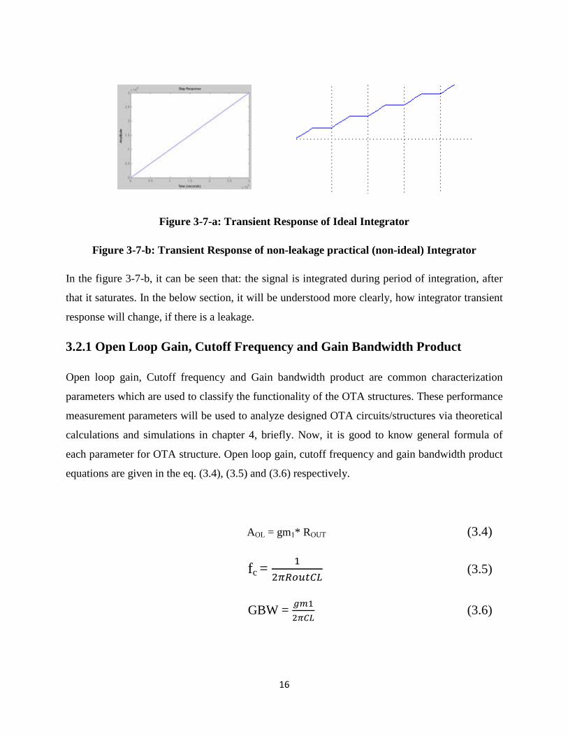
FIGURE 3-7-a Transient Response of Ideal Integrator…………………………………………..16
FIGURE 3-7-b Transient Response of non-leakage practical (non-ideal) Integrator…………….16
FIGURE 3-8 Bode and Transient Response Plots of Integrators with different gains…………17
FIGURE 3-9 Bode and Transient Response Plots of Integrators with different cutoff
frequency…………………………………………………………………………………………17
FIGURE 3-10 Transient Response of Integrator with different current leakage………………...18
FIGURE 3-11 Transient Responses of Integrator with different output resistance……………...19
FIGURE 4-1 Integrator Structure……………………………………………………………...21
FIGURE 4-2 Top Level Circuit Diagram of Integrator (Test Bench)…………………………22
FIGURE 4-3 Conventional Telescopic OTA………………………………………………….23
vii
FIGURE 4-4 Implemented Conventional Telescopic OTA schematic…..……………………24
FIGURE 4-5 High Frequency model of Cascode Stage………………………………………26
FIGURE 4-6 Schematic of Improved Telescopic Operational Transconductor Amplifier……27
FIGURE 4-7 Schematic of Improved Telescopic Operational Transconductor Amplifier……28
FIGURE 4-8 Small Signal half- equivalent circuit of the Conventional Telescopic OTA……29
FIGURE 4-9 Small Signal half- equivalent circuit of the Improved Telescopic OTA………..29
FIGURE 4-10 Schematic of Regulated Cascode Operational Transconductor Amplifier……...31
FIGURE 4-11 Performance of Regulated Cascode, Cascode and Single Transistor [20]……...32
FIGURE 4-12 Schematic of Regulated Cascode OTA in Cadence…………………………….32
FIGURE 4-13 Output Resistance as a function of the output voltage for the RGC and The OBC
OTA, respectively [22]…………………………………………………………………………..33
FIGURE 5-1 Bode Plot of the Conventional Telescopic OTA………………………………..35
FIGURE 5-2 Transient Response of the Conventional Telescopic OTA……………………..36
FIGURE 5-3 Bode Plot of the Conventional Telescopic OTA……………………………….37
FIGURE 5-4 Transient Response of the Improved Conventional Telescopic OTA………….38
FIGURE 5-5 Bode Plot of the Regulated Cascode OTA……………………………………..38
FIGURE 5-6 Transient Response of the Regulated Cascode Telescopic OTA………………39
FIGURE 5-7 Bode Plots of the designed OTAs, Conventional Telescopic (Black), Improved
Telescopic (Green) and Regulated Cascode (Red) OTA……………………………………….40
FIGURE 5-8 Transient Responses of the designed OTAs, Conventional Telescopic
(Black),Improved Telescopic (Green) and Regulated Cascode (Red) OTA……………………41
viii
List of Tables
TABLE 2.1 Features and Benefits of UWB Technology [7]……………………………………...4
TABLE 3.1 Integrator Topologies with Tradeoff [19]…………………………………………...13
TABLE 3.2 Gm (Transconductance) Topologies for Different Parameters……………………..14
TABLE 3.3 Getting Lower Current Leakages……………………………………………………20
TABLE 4.1 High Speed Designs [20]……………………………………………………………24
TABLE 5.1 Hand Calculations of OTAs………………………………………………………...42
TABLE 5.2 Simulation Results of OTAs………………………………………………………...42
ix
List of Abbreviations
BER Bit Error Rate
UWB Ultra Wideband
IR Impulse Radio
RX Receiver
WSN Wireless Sensor Networks
MB-OFDM Multi-Band Orthogonal Frequency Division Multiplexing
WLAN Wireless Local Area Network
OOK On-Off Keying
PPM Pulse Position Modulation
IC Integrated Circuit
WPAN WirelessPersonal Area Network
BER Bit Error Rate
SNR Signal to Noise Ratio
LNA Low Noise Amplifier
VGA Voltage Gain Amplifier
BPF Band Pass Filter
S-H Sample and Hold
ADC Analog to Digital Converter
BW Bandwidth
OTA Operational Transconductance Amplifier
x
Opamp Operational Amplifier
CMFB Common Mode Feedback
GBW Gain Bandwidth Product
AOL Open Loop Gain
SR Slew Rate
fc Cutoff Frequency
ROUT Output Resistance
CL Load Capacitance
Gm Transconductance
Vinp Positive Input Voltage
Vinn Negative Input Voltage
VGS Gate to Source Voltage
VT Threshold Voltage
L Channel Length
IDS Drain to Source Current
RGC Regulated Cascode
FBC Fixed Biased Cascode
OBC Optimally Biased Cascode

1
CHAPTER 1
INTRODUCTION
1.1 Background
The concept of Ultra-Wideband (UWB) was formulated in the early 1960s through research in
time-domain electromagnetics and receiver design. Through this work, the first UWB
communications patent was awarded for the short-pulse receiver [23]. After that time, UWB was
referred in broad terms as “carrierless” or impulse technology. Even though the knowledge has
been in existence for over thirty years, Ultra Wideband-Impulse Radio (UWB-IR) is an emerging
technology that has been introduced in wireless sensor networks design to reduce the power
consumption and improve the communication capabilities [1]. Nowadays, UWB receiver is
mostly used with coherent or non-coherent structure. Coherent based receiver offer long range
and better Bit Error Rate performance in noisy channel conditions. But these types of receivers
have higher complexity which causes higher cost and higher power consumption. In many
applications where cost and energy consumption are critical, non-coherent receivers are desirable
even though they may have shorter communication range and inferior performance under certain
channel conditions [24]. In this project, non-coherent energy receiver is used because it allows
simple circuit architecture that does not require a frequency synthesizer and a signal template for
integration. In non-coherent differential architecture based receiver, the integrator is the one of
the important analog block. Due to high frequency requirement, integrator is implemented using
Gm-C structure. In this structure, operational transconductance amplifier is used for Gm. The
operational amplifier is the block with the highest power consumption in analog integrated
circuits in many applications. Thanks to the low power consumption, telescopic operational
transconductance amplifier is chosen instead of two stage and folded-cascode OTA. During
integration, discharging (current leakage) is occurring on the Sample-Hold capacitors. These
current leakages can be higher or lower according to the OTA performance. This thesis project
targets to identify effects of OTA parameters on the current leakage. The most important OTA
parameters which have a contribution on the current leakage are defined in system level analysis.

2
According to this system level feedback, different Telescopic (Cascode) OTA circuits are
implement and their current leakage and parameters are compared.
1.1 Thesis Outline
This thesis project covers the theoretical analysis, system level and circuit level design of Gm-C
Integrator and OTA design for non-coherent ultra-wideband receiver.
Chapter 2 gives overview of the ultra-wideband impulse radio (UWB-IR) receiver technology
including fundamental theories and architectures for receiver.
Chapter 3 presents different type of integrators and effect of various parameter of OTA are
analyzed and the corresponding solutions for current leakage are discussed.
Chapter 4 presents the details of circuit level design of different implemented Gm-C Integrator.
Conventional Telescopic OTA, Improved Telescopic OTA and Regulated Telescopic OTA are
implemented at transistor level. Furthermore, their signal analyses are given in this chapter.
Chapter 5 offers the transistor level simulation results for both AC and Transient Analysis.
Current leakage calculations for all implemented OTA are given. Also, hand calculation and
simulation results are compared. Finally, some suggestions about chosen of OTA parameters to
decrease current leakage (discharging) are given according to the results.
3
CHAPTER 2
OVERVIEW OF THE ULTRA-WIDEBAND IMPULSE RADIO
(UWB-IR) RECEIVER TECHNOLOGY
This chapter gives an overview of the ultra-wideband impulse radio receiver technology. Firstly,
it begins with an introduction of the ultra-wideband technology. Secondly, due to importance and
relations with integrator, both UWB receiver modes and modulation techniques are discussed.
Thirdly, UWB-IR RX Architecture is described.
2.1 Ultra-Wideband Impulse Radio Technology Overview
Ultra-wideband communication (UWB) is an emerging technology and research topic; however
the knowledge of UWB has been existence for over forty years. It has been introduced in
Wireless Sensor Networks (WSN) design as a way to reduce the power consumption and improve
the communication capabilities with respect to narrow band systems [1] and Multi-Band (MB-
OFDM) [2][3]. The UWB systems can be classified into Impulse Radio (IR) and Orthogonal
Frequency Division Multiplexing (OFDM) based system. Whereas the OFDM based UWB
system is suitable to high data rate communication, the UWB-IR is appropriate solution for low
rate and low power applications. [4] Unlike classical radio systems, the UWB-IR receiver does
not require a down conversion stage. This means that a local oscillator in the receiver can be
omitted and as a result UWB-IR receiver can be implemented in low cost complementary metal
oxide-semiconductor (CMOS) [5][6]. The important features and their benefits of UWB
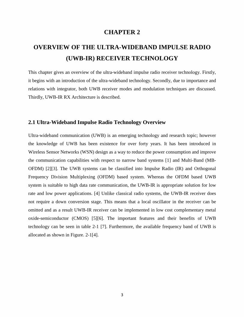
technology can be seen in table 2-1 [7]. Furthermore, the available frequency band of UWB is
allocated as shown in Figure. 2-1[4].

4
Figure 2-1: The allocated UWB spectrum [4]
As seen from Figure. 2-1, 3.1~10.6 GHz band can be used except 5-6 GHz ISM band assigned
for WLAN applications. Therefore, overall bands are composed of 3.1~5 GHz lower band and
6~10.6 GHz higher band.
Table 2-1: Features and Benefits of UWB Technology
Features Benefits High Speed Throughput in short range Fast, High Quality Transfer
Low Power Consumption Long Battery Life for Portable Devices
CMOS Technology Low Cost
Low Complexity Low Design Time
Wired Connectivity Options Convenience and Flexibility
5
2.2 UWB Receiver Architectures/Modes and Modulation Techniques
In the previous researches and literature, it is easy to find different receiver architecture such as
super regenerative architecture, coherent, semi coherent and non-coherent architectures. It is
important to decide which receiver architecture more appropriate for investigated application.
Moreover, it is needed to decide carefully which modulation techniques will be used with the
chosen receiver architecture. There is numerous modulation techniques can be used with UWB-
IR, On-Off Keying (OOK) and Pulse Position Modulation (PPM) are two of them. OOK and
PPM are popular UWB modulation techniques due to their simplicity and flexibility towards duty
cycle pulsed communication system [8]. In this project a 0.66nJ/bit non-coherent energy receiver
that works with PPM and OOK modulation a data rate up to 33Mb/s has been designed. For more
details, please check reference [3] which is written by IPack Vinn Excellence Center researches.
In the below sections, more details and explanations can be found about different receiver modes
and modulation techniques.
2.2.1 Receiver Architectures/Modes
Super-Regenerative architectures using OOK modulation use a self-oscillation induced by the
incoming signal and proportional to its power and frequency [9]. This architecture can achieve
low energy per bit but has low immunity to external interferences. Coherent architecture shows a
better sensitivity and performance but the synchronization usually requires higher circuit
complexity that can increase the power consumption [3]. The template signal generation is a kind
a disadvantage of coherent architecture. The template signal generation requires a channel
estimation which is highly complex to predict due to energy dispersion over multiple delayed
paths [3] [10]. Non-Coherent architecture allows simple circuit architecture that does not require
a frequency synthesizer and a signal template for integration. Furthermore, it can be operated
with smaller current consumption [11] [12].

6
2.2.2 Modulation Techniques
On Off Keying (OOK) is the most simple modulation technique where a pulse is transmitted to
represent/determined a binary ‘1’ and where no pulse is transmitted represent/determined a
binary ‘0’. Simplicity of physical implementation of OOK is the biggest advantage which it has.
However, there are some system drawbacks. Synchronization can be easily lost if the data
contains a steady stream of “0’s.” Also, Bit Error Rate (BER) performance of OOK is worse than
PPM. OOK can be used both for non-coherent, semi-coherent and coherent receive mode. OOK
timing in different receive modes can be seen in figure 2-2.
Figure 2-2: OOK timing in different receive modes [13]
In non-coherent mode using OOK modulation, energy is integrated over several pulses. Integrator
is not closed between pulses, giving relaxed timing requirements. On the other hand, non-
coherent detection requires a good estimation of the integrator threshold. Non-coherent detection
can be achieved by setting the pulse clock equal to the symbol clock using a long integration
window. In semi-coherent mode using OOK modulation, energy is integrated over one or several
pulses. Integrator is only active over a small window around the time where the pulse is expected
to arrive. This gives a better signal to noise ratio (SNR) compared to non-coherent detection and
allow more accurate positioning, however requires a more accurate timing circuit [13].
Pulse Position Modulation is a modulation technique where timing of the each pulse is changed
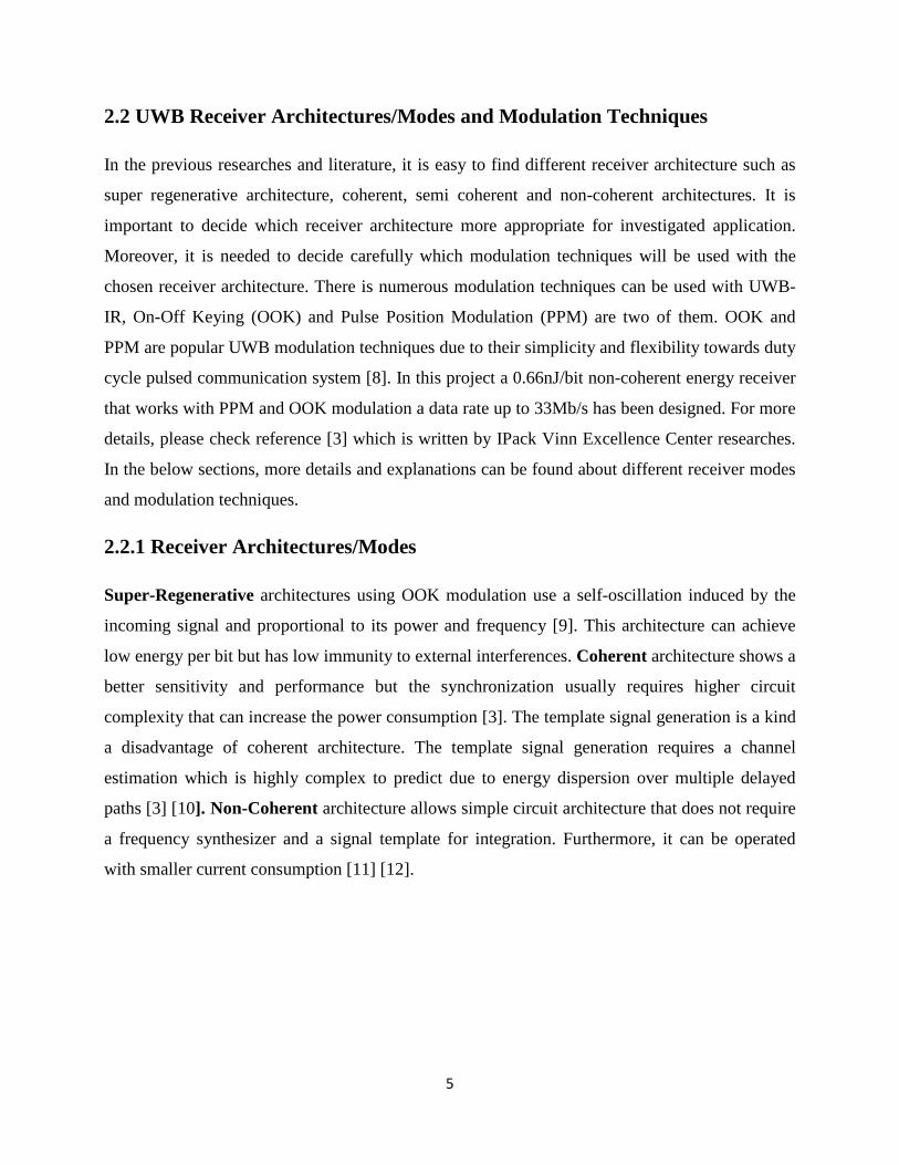
to transmit data instead of varying the amplitude. In PPM, the information in the transmitted
signal is determined by position of pulses. Figure 2-3 shows the timing for semi coherent
reception of a PPM modulated signal. In this example a logical ‘0’ is represented by one pulse
position (black curve) and logical ‘1’ is represented by another position (gray curve).
7
Figure 2-3: PPM timing in semi coherent receive mode [13]
In this project for PPM modulation, two interleaved integrators are used. Depending on which
pulse position contains the most energy, one of the integrators will have a higher final output
value. The advantage of the pulse position modulation compared to on-off keying is that no
threshold level is needed to distinguish between one and zero.
2.3 UWB-IR Receiver Architecture Description
In this project, the receiver (RX) is based on a non-coherent differential architecture. In the
receiver, the signal is amplified by the Low Noise Amplifier (LNA) and Voltage Gain Amplifier
(VGA), squared by the four quadrant multiplier and then integrated by a bank of 4 integrators.
Figure 2-4 shows the RX architecture.
Figure 2-4: Receiver Architecture [3]

8
The receiver has been designed to work with UWB-IR passive sensor tags introduced in [14],
inside the 3.1-4.8 GHz band. The incoming signal is received by antenna and a Band Pass Filter
(BPF) which is working for 3.1-4.8GHz, is used to remove out of band interferences. The
resulting signal is amplified, rectified and integrated respectively. This signal amplified by LNA
and VGA. LNA and VGA provide the required gain that compensates the analog multiplier
attenuation based on the incoming signal strength. Then, it is rectified by multiplier/square circuit
which drives the integrator. After that, signal which is an output of the multiplier integrated by
integrator. Two independent multiplier circuits have been used for each integrator to avoid circuit
over-loading which significantly reduces the bandwidth (BW) and increases the signal
attenuation. Using Sample and Hold (S-H) capacitor the final analog voltage is stored. This
voltage is then amplified and sampled by a differential Analog to Digital Converter (ADC) for bit
evaluation.
9
CHAPTER 3
OVERVIEW OF THE INTEGRATOR AND SYSTEM LEVEL
DESIGN OF INTEGRATOR
This chapter will explain integrator which is the important building block for UWB Receiver.
Firstly, the simplest passive RC integrator will be described. Secondly, Active Opamp-C
integrator will be explained. Thirdly, Gm (OTA) - C integrator which is used in this project will
be given, with brief explanation why it is more suitable for UWB applications. Finally, the
important parameters of OTA which cause a current leakage (discharging) and their affects will
be discussed.
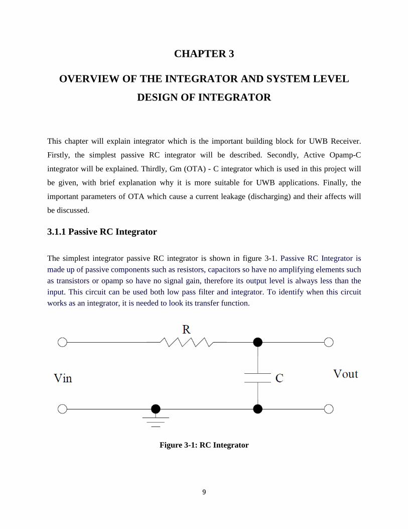
3.1.1 Passive RC Integrator
The simplest integrator passive RC integrator is shown in figure 3-1. Passive RC Integrator is made up of passive components such as resistors, capacitors so have no amplifying elements such as transistors or opamp so have no signal gain, therefore its output level is always less than the input. This circuit can be used both low pass filter and integrator. To identify when this circuit works as an integrator, it is needed to look its transfer function.
Figure 3-1: RC Integrator

10
The corresponding transfer function relating the output voltage to the input voltage is given by
Eq. (3.1).
Vo(s)Vi (s)
= 11+RCs
(3.1)
The circuits acts as an integrator if RCs ≫ 1 or equivalently for Eq. (3.2) [15]
W = 2πf ≫ 1RC
rad/s (3.2)
In other words, passive RC circuit acts as integrator only for signals with frequency 10 times higher than cutoff frequency of passive RC circuit (low pass filter). To understand when exactly this circuit works as an integrator, frequency response curve (bode plot) of RC is given in figure 3-2. After the cut off frequency point, there is a slope of -20 dB/decade where the circuit works as an integrator.
Figure 3-2: Bode Plot of RC Integrator [16]
11
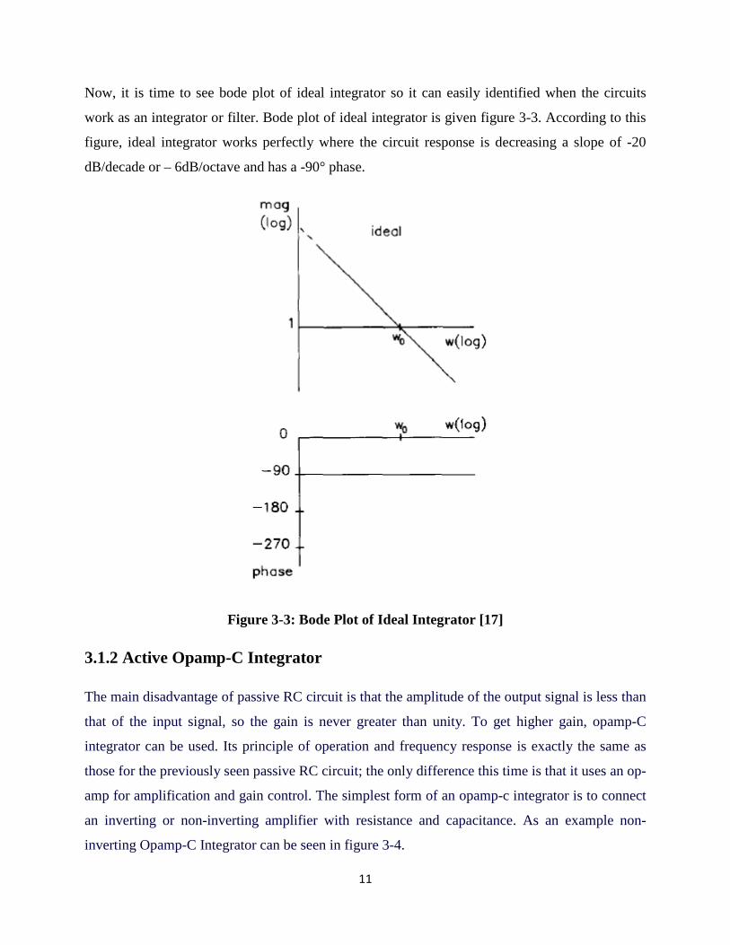
Now, it is time to see bode plot of ideal integrator so it can easily identified when the circuits
work as an integrator or filter. Bode plot of ideal integrator is given figure 3-3. According to this
figure, ideal integrator works perfectly where the circuit response is decreasing a slope of -20
dB/decade or – 6dB/octave and has a -90° phase.
Figure 3-3: Bode Plot of Ideal Integrator [17]
3.1.2 Active Opamp-C Integrator
The main disadvantage of passive RC circuit is that the amplitude of the output signal is less than
that of the input signal, so the gain is never greater than unity. To get higher gain, opamp-C
integrator can be used. Its principle of operation and frequency response is exactly the same as
those for the previously seen passive RC circuit; the only difference this time is that it uses an op-
amp for amplification and gain control. The simplest form of an opamp-c integrator is to connect
an inverting or non-inverting amplifier with resistance and capacitance. As an example non-
inverting Opamp-C Integrator can be seen in figure 3-4.
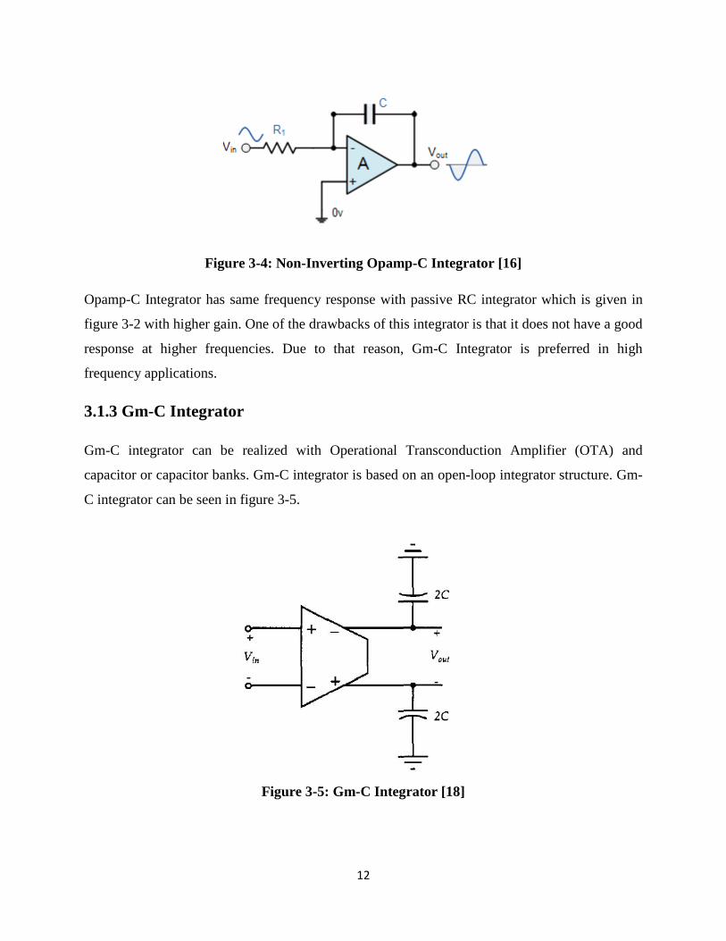
12
Figure 3-4: Non-Inverting Opamp-C Integrator [16]
Opamp-C Integrator has same frequency response with passive RC integrator which is given in
figure 3-2 with higher gain. One of the drawbacks of this integrator is that it does not have a good
response at higher frequencies. Due to that reason, Gm-C Integrator is preferred in high
frequency applications.
3.1.3 Gm-C Integrator
Gm-C integrator can be realized with Operational Transconduction Amplifier (OTA) and
capacitor or capacitor banks. Gm-C integrator is based on an open-loop integrator structure. Gm-
C integrator can be seen in figure 3-5.
Figure 3-5: Gm-C Integrator [18]
13
In this integrator structure, a transconductor produces a current proportional to the differential
input voltage and the output is taken across the integrating capacitors. If the transconductor is
ideal with a transconductance equal to Gm, the transfer function of integrator can be gives as in
the eq. (3.3).
H(s) = 𝐺𝑚𝑠𝐶
(3.3)
Since the Gm-C integrator is an open-loop integrator, it has the potential for very high speeds.
Furthermore, the transconductor has to drive only capacitive loads; however, the integrator unity
gain frequency is sensitive to parasitic capacitances. Tradeoff between different integrator
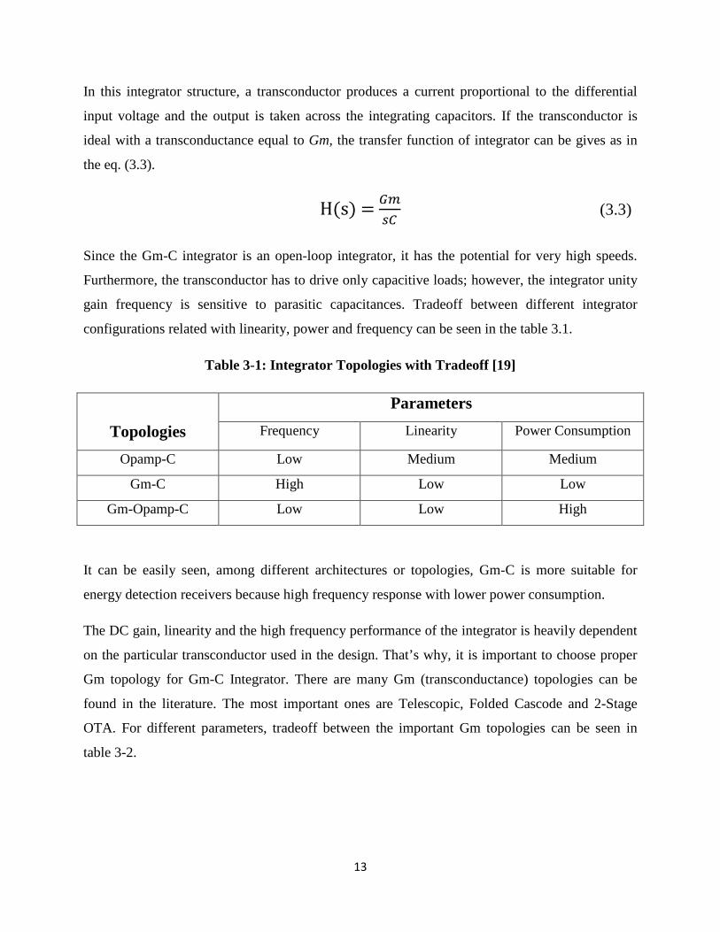
configurations related with linearity, power and frequency can be seen in the table 3.1.
Table 3-1: Integrator Topologies with Tradeoff [19]
Topologies
Parameters Frequency Linearity Power Consumption
Opamp-C Low Medium Medium
Gm-C High Low Low
Gm-Opamp-C Low Low High
It can be easily seen, among different architectures or topologies, Gm-C is more suitable for
energy detection receivers because high frequency response with lower power consumption.
The DC gain, linearity and the high frequency performance of the integrator is heavily dependent
on the particular transconductor used in the design. That’s why, it is important to choose proper
Gm topology for Gm-C Integrator. There are many Gm (transconductance) topologies can be
found in the literature. The most important ones are Telescopic, Folded Cascode and 2-Stage
OTA. For different parameters, tradeoff between the important Gm topologies can be seen in
table 3-2.

14
Table 3-2: Gm (Transconductance) Topologies for Different Parameters
Topologies Parameters
Gain Output Swing Speed Noise Distortion
Simple 2-Stage Medium High Low Medium
Folded Cascode High Medium High Medium
Telescopic High Medium High Low
The other important parameter for OTA is power consumption. There is a tradeoff between
speed, power and gain too for OTA design and these parameters are usually contradicting
parameters. The telescopic amplifier consumes the least power compared with the other two
OTA. In this project, Gm-cell is implemented with telescopic/cascode OTA to get higher speed.
Also, a Common Mode Feedback (CMFB) based on a differential continuous time topology is
added to Gm-Cell to provide enough common mode gain and maintain a steady DC operating
point. Brief explanation about OTA and CMFB design for this project is given in the chapter 4.
3.2 System Level Design of Integrator
System level analyze has been done in this project to identify which parameters of circuit has an
effect on the current leakage (discharging) in the integrator. This current leakage is occurring
during S-H capacitors are discharging. This leakage decreases the performance of the receiver.
The most important circuit parameters which create leakage and limit overall all performance of
the receiver are investigated. These parameters are Open Loop Gain (AOL), Cutoff Frequency (fc),
Gain Bandwidth Product (GBW), Output Resistance (ROUT), and Slew Rate (SR). In the below
section, how these parameters affect leakage is explained. Furthermore, to decrease leakage,
appropriate way to choose parameters is given for optimum circuit level design. Before looking
effect of these parameters, it is necessary to know ideal and practical (non-ideal) integrator
transient and frequency responses. Frequency and phase response plots of ideal and practical
integrator are given in figure 3-6.
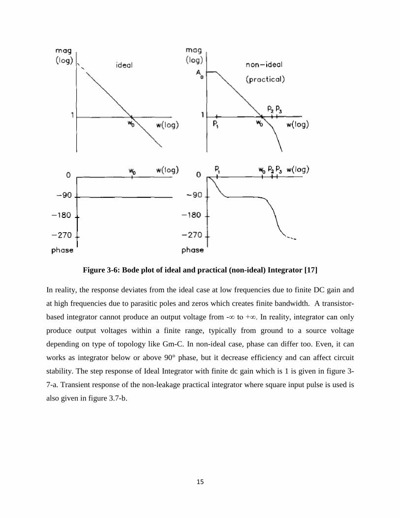
15
Figure 3-6: Bode plot of ideal and practical (non-ideal) Integrator [17]
In reality, the response deviates from the ideal case at low frequencies due to finite DC gain and
at high frequencies due to parasitic poles and zeros which creates finite bandwidth. A transistor-
based integrator cannot produce an output voltage from -∞ to +∞. In reality, integrator can only
produce output voltages within a finite range, typically from ground to a source voltage
depending on type of topology like Gm-C. In non-ideal case, phase can differ too. Even, it can
works as integrator below or above 90° phase, but it decrease efficiency and can affect circuit
stability. The step response of Ideal Integrator with finite dc gain which is 1 is given in figure 3-
7-a. Transient response of the non-leakage practical integrator where square input pulse is used is
also given in figure 3.7-b.
16
Figure 3-7-a: Transient Response of Ideal Integrator
Figure 3-7-b: Transient Response of non-leakage practical (non-ideal) Integrator
In the figure 3-7-b, it can be seen that: the signal is integrated during period of integration, after
that it saturates. In the below section, it will be understood more clearly, how integrator transient
response will change, if there is a leakage.
3.2.1 Open Loop Gain, Cutoff Frequency and Gain Bandwidth Product
Open loop gain, Cutoff frequency and Gain bandwidth product are common characterization
parameters which are used to classify the functionality of the OTA structures. These performance
measurement parameters will be used to analyze designed OTA circuits/structures via theoretical
calculations and simulations in chapter 4, briefly. Now, it is good to know general formula of
each parameter for OTA structure. Open loop gain, cutoff frequency and gain bandwidth product
equations are given in the eq. (3.4), (3.5) and (3.6) respectively.
AOL = gm1* ROUT (3.4)
fc = 12𝜋𝑅𝑜𝑢𝑡𝐶𝐿
(3.5)
GBW = 𝑔𝑚12𝜋𝐶𝐿
(3.6)

17
It is obvious; GBW is product of open loop gain and cutoff frequency. It is called unity gain
bandwidth too. Now, open loop gain response is investigated to identify its effect on leakage by
assuming each integrator has same unity gain bandwidth with variable DC gain. Both AC and
Transient response plots are given in the figure 3-8.
Figure 3-8: Bode and Transient Response Plots of Integrators with different gains
In the figure 3-8, one can see that, when DC gain is increased while GBW is kept constant, it has
a better transient response which is more closed to ideal one. As a result, having more gain will
decrease leakage (discharging). Now, cutoff frequency response is investigated to identify its
effect on leakage by tuning center frequency and keeping the DC gain constant, the unity gain
bandwidth will vary as shown in the figure 3-9.
Figure 3-9: Bode and Transient Response Plots of Integrators with different cutoff
frequency
18
In the figure 3-9, one can see that, when cutoff frequency is decreased while gain is kept
constant, it has a better transient response which is more closed to ideal one. As a result, having
lower cutoff frequency will decrease leakage (discharging).
3.2.2 Slew Rate
Slew rate is other common characterization parameter which is used to classify the functionality
of the OTA structures. Help of Simulink, with the same open loop gain and cutoff frequency with
different current leakage integrator is realized. Thanks to this architecture, changing of slew rate
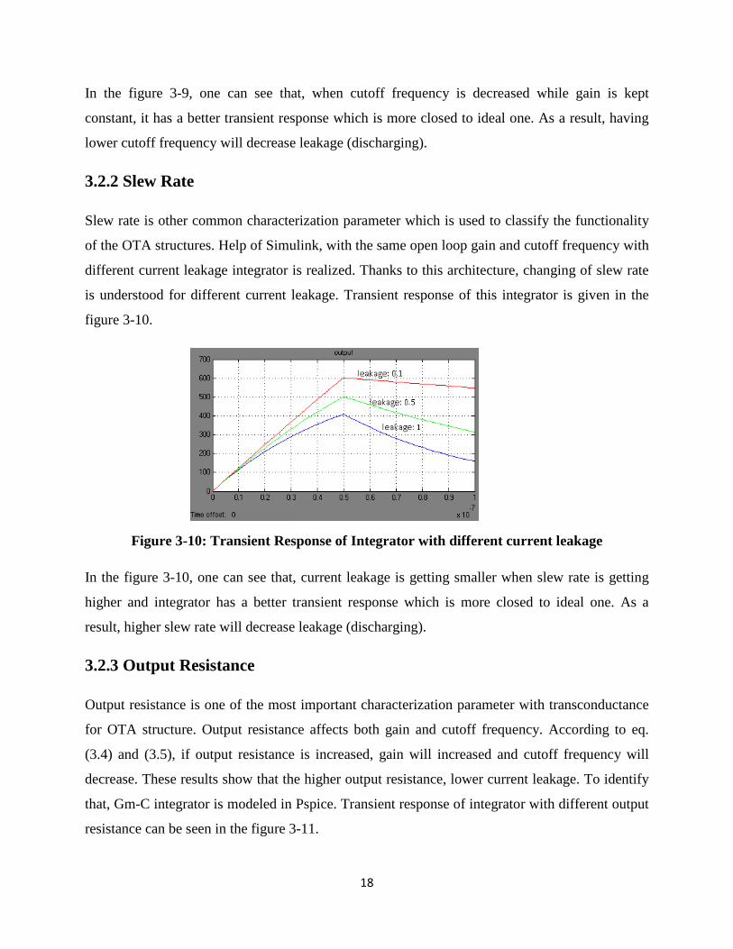
is understood for different current leakage. Transient response of this integrator is given in the
figure 3-10.
Figure 3-10: Transient Response of Integrator with different current leakage
In the figure 3-10, one can see that, current leakage is getting smaller when slew rate is getting
higher and integrator has a better transient response which is more closed to ideal one. As a
result, higher slew rate will decrease leakage (discharging).
3.2.3 Output Resistance
Output resistance is one of the most important characterization parameter with transconductance
for OTA structure. Output resistance affects both gain and cutoff frequency. According to eq.
(3.4) and (3.5), if output resistance is increased, gain will increased and cutoff frequency will
decrease. These results show that the higher output resistance, lower current leakage. To identify
that, Gm-C integrator is modeled in Pspice. Transient response of integrator with different output
resistance can be seen in the figure 3-11.
19
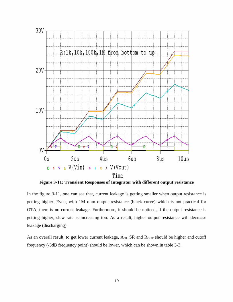
Figure 3-11: Transient Responses of Integrator with different output resistance
In the figure 3-11, one can see that, current leakage is getting smaller when output resistance is
getting higher. Even, with 1M ohm output resistance (black curve) which is not practical for
OTA, there is no current leakage. Furthermore, it should be noticed, if the output resistance is
getting higher, slew rate is increasing too. As a result, higher output resistance will decrease
leakage (discharging).
As an overall result, to get lower current leakage, AOL, SR and ROUT should be higher and cutoff
frequency (-3dB frequency point) should be lower, which can be shown in table 3-3.

20
Table 3-3: Getting Lower Current leakage
To get Lower Current Leakage (discharging)
Open Loop Gain High
Cutoff Frequency Low
Slew Rate High
Output Resistance High
It is obvious, increasing output resistance will increase both open loop gain and slew rate and
decrease cutoff frequency. So the most important parameter is Output resistance to decrease
current leakage. According to this knowledge, the new improved circuit which has a higher ROUT
is designed and compared with conventional circuit in Chapter 4.
21
CHAPTER 4
INTEGRATOR CIRCUIT LEVEL DESIGN
This chapter will explain circuit level design of integrator which is the important building block
for UWB Receiver. Firstly, integrator circuit structure will be described. But this chapter
generally will focus on the most important circuit block OTA design and its signal analysis.
There are three different OTA circuit is implemented in this project to compare and identify
current leakage in the circuit level. Secondly, first implemented Conventional Telescopic
(Cascode) OTA design will be given in details. Thirdly, second implemented Improved
Telescopic OTA design will be described. After that, last implemented Regulated Cascode OTA
will be explained. Finally, a Common Mode Feedback (CMFB) circuit will be mentioned.
4.1 Integrator Circuit Structure
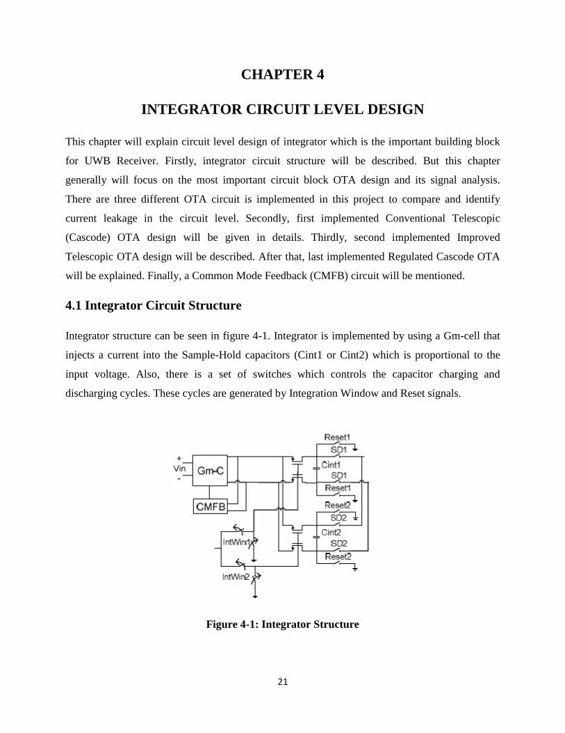
Integrator structure can be seen in figure 4-1. Integrator is implemented by using a Gm-cell that
injects a current into the Sample-Hold capacitors (Cint1 or Cint2) which is proportional to the
input voltage. Also, there is a set of switches which controls the capacitor charging and
discharging cycles. These cycles are generated by Integration Window and Reset signals.
Figure 4-1: Integrator Structure

22
There is a switch resistance between Gm-cell and the Sample-Hold capacitor, which can be used
to modify integrator RC constant. Common Mode Feedback Circuit is another circuit block
which is added to provide enough common-mode gain and maintain a steady DC operating point.
The Gm-cell is implemented with three different Operational Transconductance Amplifiers
(OTA), each of them is explained in below sections. Same top level circuit diagram of integrator
which can be seen in figure 4-2 is used in Cadence to test integrator with different OTAs.
Figure 4-2: Top Level Circuit Diagram of Integrator (Test Bench)
23
4.2 Conventional Telescopic (Cascode) OTA
A conventional, fully differential Telescopic, Operational Transconductance Amplifier (OTA)
configuration is shown in figure 4-3.
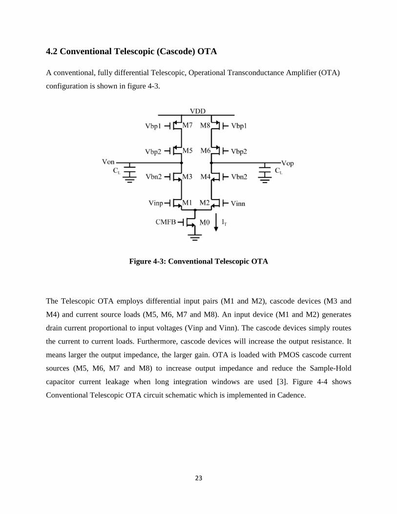
Figure 4-3: Conventional Telescopic OTA
The Telescopic OTA employs differential input pairs (M1 and M2), cascode devices (M3 and
M4) and current source loads (M5, M6, M7 and M8). An input device (M1 and M2) generates
drain current proportional to input voltages (Vinp and Vinn). The cascode devices simply routes
the current to current loads. Furthermore, cascode devices will increase the output resistance. It
means larger the output impedance, the larger gain. OTA is loaded with PMOS cascode current
sources (M5, M6, M7 and M8) to increase output impedance and reduce the Sample-Hold
capacitor current leakage when long integration windows are used [3]. Figure 4-4 shows
Conventional Telescopic OTA circuit schematic which is implemented in Cadence.

24
Figure 4-4: Implemented Conventional Telescopic OTA schematic
For UWB Receiver, high speed OTA is necessary. In this project when designing each OTA
circuit, overdrive voltage (VGS-VT) of input devices and channel length (L) of transistors values
are selected carefully according to the table 4-1.
Table 4-1: High Speed Design [20]
High Gain High Speed
VGS-VT Low (0.2V) High (0.5V)
L High Low
It is striking that for high frequency (UWB) design, a large VGS-VT is required and the lowest
possible value of channel length L. This is exactly the opposite of what is required for high gain
[20]. It is good to remember that, setting the values of VGS-VT is the same as setting ratio of
gm/IDS. Signal analysis of telescopic OTA is given below section. In this signal analysis part, the
most important and related parameters of OTA for current leakage are chosen. Hand calculation

25
of each parameter can be found in Appendix. Furthermore, results are given and compared in
simulation and result chapter 5.
4.2.1 Open Loop Gain (AOL)
Open loop gain is one of the most important parameter for OTA design. In the OTA circuit,
output current is given by equation 4.1.
iout = id1 –id2 (4.1)
where:
id1 = gm1Vi(+), id2 = gm2Vi(-), (4.2)
Assuming: gm1=gm2, and substituting (4.2) into (4.1):
iout = gm1(Vi(+) - Vi(-)) (4.3)
The output resistance is given by Eq. 4.4
ROUT = { [ [ 1 + (gm3 + gmbs3)*ro3]*ro1 + ro3 } || { [ [ 1 + (gm5 + gmbs5)*ro5]*ro7 + ro5 }
which is simplified ROUT ≈ (gm3*ro3*ro1) || (gm5*ro5*ro7) (4.4)
Combining (4.3) and (4.4), the output voltage is then given by:
vout = iout Rout = gm1(Vi(+) - Vi(-))(gm3*ro3*ro1) || (gm5*ro5*ro7) (4.5)
and the open loop gain is:
AOL = 𝑣𝑜𝑢𝑡𝑣𝑖𝑛
= gm1 (gm3*ro3*ro1) || (gm5*ro5*ro7) (4.6)

26
4.2.2 Bandwidth
High frequency of cascode stage is investigated clearly in [21]. Here, critical pole frequency
equations are given with output frequency (cutoff frequency). High frequency model of cascode
stage can be seen in figure 4-5.
Figure 4-5: High Frequency model of Cascode Stage
At node A, the implemented circuit has another input capacitance which is parallel to CGS1. So
the pole associated with node A is given by Eq. 4.7
Wp,A = 1
𝑅𝑠[(𝐶𝐺𝑆1+𝐶𝑖𝑛)+�1+ 𝑔𝑚1𝑔𝑚2+𝑔𝑚𝑏2�𝐶𝐺𝐷1]
(4.7)
At node X, the pole is calculated with Eq. 4.8
Wp,X = 𝑔𝑚2+𝑔𝑚𝑏22𝐶𝐺𝐷1+𝐶𝐷𝐵1+𝐶𝑆𝐵2+𝐶𝐺𝑆2
(4.8)
Finally output node creates a third pole which is dominant pole/bandwidth of the OTA is given
by Eq. 4.9
Wp,out = 1𝑅𝑜𝑢𝑡(𝐶𝐷𝐵2+𝐶𝐺𝐷2+𝐶𝐿+𝐶𝑠)
(4.9)

27
4.2.3 Gain Bandwidth Product (GBW)
GBW is product of open loop gain and bandwidth. Equations (4.6) and (4.9) are combined for the
gain bandwidth product (GBW) which is given Eq. 4.10
GBW = 𝑔𝑚12𝜋(𝐶𝐷𝐵2+𝐶𝐿+𝐶𝐺𝐷2)
(4.10)
4.2.4 Maximum Output Current and Slew Rate
The maximum output current of the conventional Telescopic OTA is limited by the bias current
and given by Eq. 4.11.
IOUT MAX = I BIAS /2 (4.11)
The slew rate (SR) is given by Eq. 4.12
SR = IOUT MAX 𝐶𝐿
(4.12)
4.3 Improved Telescopic (Cascode) OTA
An improved, fully differential Telescopic, Operational Transconductance Amplifier (OTA)
configuration is shown in figure 4-6.
Figure 4-6: Schematic of Improved Telescopic Operational Transconductor Amplifier
28
From figure 4-6, one can find that a PMOS differential pair is introduced as compared with the
conventional telescopic OTA. The PMOS differential pair injects current into nodes A and B,
which helps improve the gain of the amplifier. Furthermore, the PMOS differential does not
consume additional power and the power consumption of the improved design is the same as the
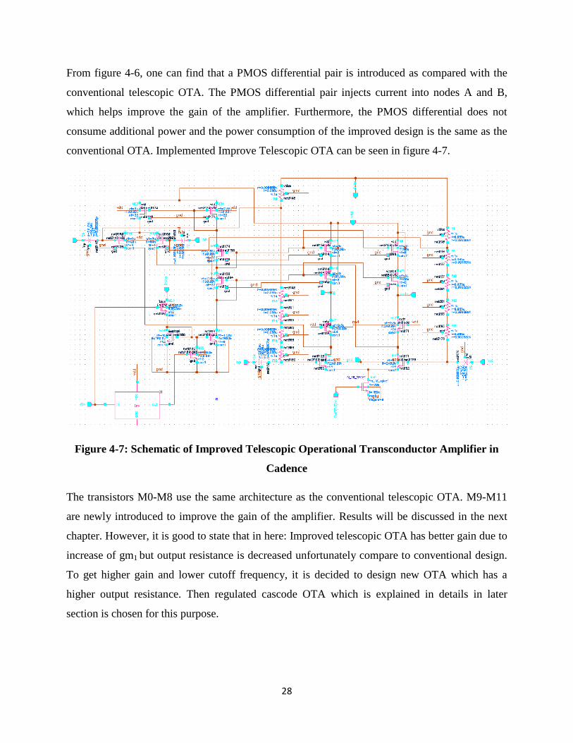
conventional OTA. Implemented Improve Telescopic OTA can be seen in figure 4-7.
Figure 4-7: Schematic of Improved Telescopic Operational Transconductor Amplifier in
Cadence
The transistors M0-M8 use the same architecture as the conventional telescopic OTA. M9-M11
are newly introduced to improve the gain of the amplifier. Results will be discussed in the next
chapter. However, it is good to state that in here: Improved telescopic OTA has better gain due to
increase of gm1 but output resistance is decreased unfortunately compare to conventional design.
To get higher gain and lower cutoff frequency, it is decided to design new OTA which has a
higher output resistance. Then regulated cascode OTA which is explained in details in later
section is chosen for this purpose.

29
4.3.1 Open Loop Gain (AOL)
Additional PMOS differential pair will contribute to Gm. To identify contribution, it is better to
look small signal equivalent of both conventional and improved OTA. Figure 4-8 shows small
signal equivalent circuits of the conventional OTA and figure 4-9 shows small signal equivalent
circuits of the improved OTA.
Figure 4-8: Small Signal half- equivalent circuit of the Conventional Telescopic OTA
Figure 4-9: Small Signal half- equivalent circuit of the Improved Telescopic OTA
Compared with Fig. 4-8, there is an additional PMOS transistor whose drain is connected to M3
transistor’s gate. So the new Gm is given by Eq. 4.13
Gm = gm1 +gm10 (4.13)
What’s more, new output resistance is given Eq. 4.14
ROUT ≈ (gm3*ro3*(ro1||ro10)) || (gm5*ro5*ro7) (4.14)
As a result, open loop gain for new improved circuit is given Eq. 4.15
AOL = GmROUT = (gm1 +gm10) (gm3*ro3*(ro1||ro10)) || (gm5*ro5*ro7) (4.15)
30
4.3.2 Bandwidth
A new additional PMOS differential pair will affect only X node which is farther from the other
two nodes. Now, X node will be moved a little bit farther from the others too. So, it will not
affect frequency response. But due to the change in output resistance, dominant pole/bandwidth
of the OTA will change and it moves to the right and get higher cutoff frequency. The new
equations for poles are given Eq. 4.16, 4.17 and 4.18 respectively.
Wp,A = 1
𝑅𝑠[(𝐶𝐺𝑆1+𝐶𝑖𝑛)+�1+𝑔𝑚1+𝑔𝑚10𝑔𝑚3+𝑔𝑚𝑏3�𝐶𝐺𝐷1]
(4.16)
Wp,X = 𝑔𝑚3+𝑔𝑚10+𝑔𝑚𝑏32𝐶𝐺𝐷1+𝐶𝐷𝐵1+𝐶𝑆𝐵3+𝐶𝐺𝑆3
(4.17)
Wp,out = 1𝑅𝑜𝑢𝑡(𝐶𝐷𝐵3+𝐶𝐺𝐷3+𝐶𝐿+𝐶𝑠)
(4.18)
4.3.3 Gain Bandwidth Product (GBW)
GBW is product of open loop gain and bandwidth. Equations (4.15) and (4.18) are combined for
the gain bandwidth product (GBW) which is given Eq. 4.19
GBW = 𝑔𝑚1+𝑔𝑚102𝜋(𝐶𝐷𝐵3+𝐶𝐿+𝐶𝐺𝐷3)
(4.19)
4.3.4 Maximum Output Current and Slew Rate
The maximum output current of the improved Telescopic OTA is limited both the bias current
and the current of M9 and given by Eq. 4.20.
IOUT MAX = (I BIAS - IM9 )/2 (4.20)
The slew rate (SR) is given by Eq. 4.21
SR = IOUT MAX 𝐶𝐿
(4.21)
31
4.4 Regulated Telescopic (Cascode) OTA
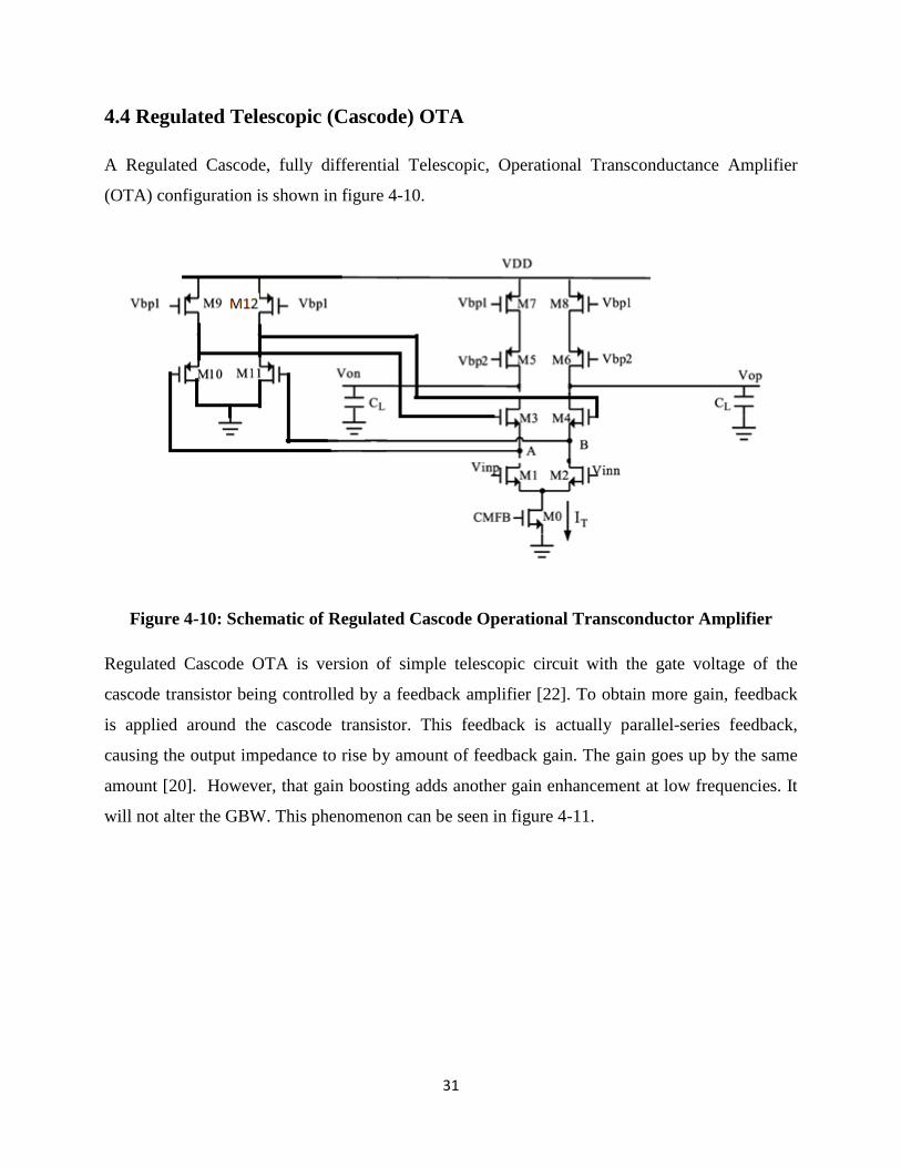
A Regulated Cascode, fully differential Telescopic, Operational Transconductance Amplifier
(OTA) configuration is shown in figure 4-10.
Figure 4-10: Schematic of Regulated Cascode Operational Transconductor Amplifier
Regulated Cascode OTA is version of simple telescopic circuit with the gate voltage of the
cascode transistor being controlled by a feedback amplifier [22]. To obtain more gain, feedback
is applied around the cascode transistor. This feedback is actually parallel-series feedback,
causing the output impedance to rise by amount of feedback gain. The gain goes up by the same
amount [20]. However, that gain boosting adds another gain enhancement at low frequencies. It
will not alter the GBW. This phenomenon can be seen in figure 4-11.
32
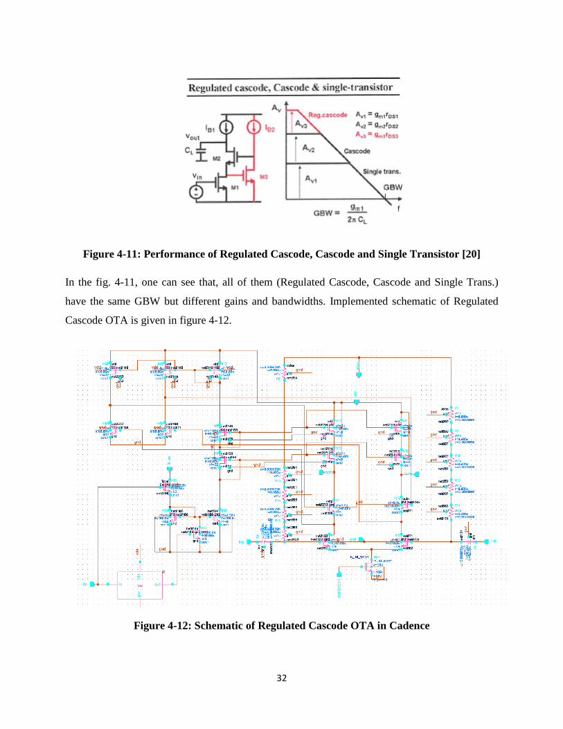
Figure 4-11: Performance of Regulated Cascode, Cascode and Single Transistor [20]
In the fig. 4-11, one can see that, all of them (Regulated Cascode, Cascode and Single Trans.)
have the same GBW but different gains and bandwidths. Implemented schematic of Regulated
Cascode OTA is given in figure 4-12.
Figure 4-12: Schematic of Regulated Cascode OTA in Cadence
33
4.4.1 Open Loop Gain (AOL)
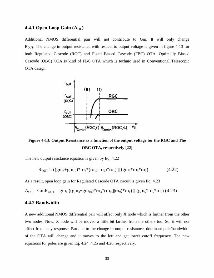
Additional NMOS differential pair will not contribute to Gm. It will only change ROUT. The change in output resistance with respect to output voltage is given in figure 4-13 for
both Regulated Cascode (RGC) and Fixed Biased Cascode (FBC) OTA. Optimally Biased
Cascode (OBC) OTA is kind of FBC OTA which is technic used in Conventional Telescopic
OTA design.
Figure 4-13: Output Resistance as a function of the output voltage for the RGC and The
OBC OTA, respectively [22]
The new output resistance equation is given by Eq. 4.22
ROUT ≈ ((gm3+gm10)*ro3*(ro10||ro9)*ro1) || (gm5*ro5*ro7) (4.22)
As a result, open loop gain for Regulated Cascode OTA circuit is given Eq. 4.23
AOL = GmROUT = gm1 ((gm3+gm10)*ro3*(ro10||ro9)*ro1) || (gm5*ro5*ro7) (4.23)
4.4.2 Bandwidth
A new additional NMOS differential pair will affect only X node which is farther from the other
two nodes. Now, X node will be moved a little bit farther from the others too. So, it will not
affect frequency response. But due to the change in output resistance, dominant pole/bandwidth
of the OTA will change and it moves to the left and get lower cutoff frequency. The new
equations for poles are given Eq. 4.24, 4.25 and 4.26 respectively.

34
Wp,A = 1
𝑅𝑠[(𝐶𝐺𝑆1+𝐶𝑖𝑛)+�1+ 𝑔𝑚1𝑔𝑚3+𝑔𝑚10+𝑔𝑚𝑏3�𝐶𝐺𝐷1]
(4.24)
Wp,X = 𝑔𝑚3+𝑔𝑚10+𝑔𝑚𝑏32𝐶𝐺𝐷1+𝐶𝐷𝐵1+𝐶𝑆𝐵3+𝐶𝐺𝑆3
(4.25)
Wp,out = 1𝑅𝑜𝑢𝑡(𝐶𝐷𝐵3+𝐶𝐺𝐷3+𝐶𝐿+𝐶𝑠)
(4.26)
4.4.3 Gain Bandwidth Product (GBW)
GBW is product of open loop gain and bandwidth. Equations (4.23) and (4.26) are combined for
the gain bandwidth product (GBW) which is given Eq. 4.19. Note that, GBW is same for
conventional Telescopic OTA and Regulated Cascode OTA due to no change in Gm.
GBW = 𝑔𝑚12𝜋(𝐶𝐷𝐵3+𝐶𝐿+𝐶𝐺𝐷3)
(4.27)
4.4.4 Maximum Output Current and Slew Rate
The maximum output current of the Regulated Cascode OTA is limited both the bias current and
the current of M9 and given by Eq. 4.28.
IOUT MAX = (I BIAS )/2 (4.28)
The slew rate (SR) is given by Eq. 4.29
SR = IOUT MAX 𝐶𝐿
(4.29)

35
CHAPTER 5
SIMULATIONS AND RESULTS
5.1 AC and Transient Analyses of Designed OTAs
Before showing analyses results, it is better to mention about input signal properties. It has 6mV
input amplitude. This value assumed to be got at the output of the squarer circuit. Furthermore,
Square pulse is used for input signal. In these analyses, 150MHz input frequency which is 10
times higher than highest cutoff frequency (15.71MHz for Improved OTA) is used. Also, to
explain importance of input signal frequency for integrator, transient responses of OTAs are
given with different input signal frequencies.
5.1.1 AC and Transient Analyses of Conventional Telescopic OTA
Figure 5-1 shows bode plot of the conventional telescopic OTA.
Figure 5-1: Bode Plot of the Conventional Telescopic OTA
Gain Margin = 31.59 dB (@-180) – 0 dB (@unity) = 31.59 dB
Phase Margin = -180° - (-287.1° (@unity gain)) = 107.1°

36
Frequency @peak= 871 KHz = 32.03 dB
Frequency @-3dBhigh= 348.2 KHz = 29.03dB
Frequency @-3dBlow= 3.166 MHz = 29.03dB
Frequency @unity gain= 1.25 GHz = 0 dB
Frequency @2GHz = 2GHz = -4.368 dB
Figure 5-2 shows Transient response of the conventional telescopic OTA
Figure 5-2: Transient Response of the Conventional Telescopic OTA

37
5.1.2 AC and Transient Analyses of Improved Conventional Telescopic OTA
Bode plot of the improved conventional telescopic OTA can be seen in figure 5-3.
Figure 5-3: Bode Plot of the Conventional Telescopic OTA
Gain Margin = 34.3 dB (@-180) – 0 dB (@unity) = 34.3 dB
Phase Margin = -180° - (-302° (@unity gain)) = 122.0°
Frequency @peak= 1.585 MHz = 34.69 dB
Frequency @-3dBhigh= 410 KHz = 29.03dB
Frequency @-3dBlow= 15.71 MHz = 29.03dB
Frequency @unity gain= 3.60 GHz = 0 dB
Frequency @2GHz = 2GHz = 5.304 dB
Transient response plot of the improved conventional telescopic OTA can be seen in figure 5-4.

38
Figure 5-4: Transient Response of the Improved Conventional Telescopic OTA
5.1.3 AC and Transient Analyses of Regulated Cascode OTA
Figure 5-5 shows bode plot of the regulated cascode OTA
Figure 5-5: Bode Plot of the Regulated Cascode OTA
Gain Margin = 35.61 dB (@-180) – 0 dB (@unity) = 35.61 dB
Phase Margin = -180° - (-295.8° (@unity gain)) = 115.8°

39
Frequency @peak= 871 KHz = 35.69 dB
Frequency @-3dBhigh= 304.1 KHz = 29.03dB
Frequency @-3dBlow= 2.23 MHz = 32.9dB
Frequency @unity gain= 1.48 GHz = 0 dB
Frequency @2GHz = 2GHz = -2.642 dB
Figure 5-6 shows Transient response of the Regulated Cascode OTA
Figure 5-6: Transient Response of the Regulated Cascode Telescopic OTA

40
5.2 Overall Results and Current Leakage (Discharging) Calculation
Figure 5-7 shows bode plots of the designed OTA together. Red one represents Regulated OTA,
Green represents Improved Telescopic OTA and finally, black curve represent Conventional
Telescopic OTA.
Figure 5-7: Bode Plots of the designed OTAs, Conventional Telescopic (Black), Improved
Telescopic (Green) and Regulated Cascode (Red) OTA
Transient response plot of the designed OTA together can be seen in figure 5-8. Again, Red one
represents Regulated OTA, Green represents Improved Telescopic OTA and finally, black curve
represent Conventional Telescopic OTA.

41
Figure 5-8: Transient Responses of the designed OTAs, Conventional Telescopic (Black),
Improved Telescopic (Green) and Regulated Cascode (Red) OTA
General formula to calculate Current Leakage (Discharging) in percentage
Current Leakage = (Discharged Voltage (Energy) at saturated cycle) / Total Integrated Voltage (Energy) until saturated cycle * %100
Note: Saturated Cycle is a cycle where total integrated energy is %10 lower than maximum total integrated energy which is calculating at transient response analysis.
Current Leakage (Discharging) Calculations for
Each Circuit where input signal is 150MHz
At Saturated Cycle: For Conventional Telescopic OTA (Black Graph)
Total Integrated voltage = 26.08mV, Discharged Voltage = 26.08mV – 24.07mV = 2.01mV
Current Leakeage = (2.01mV/26.08mV) *100% = % 7.70
At Saturated Cycle: For Regulated Cascode OTA (Red Graph)
Total Integrated voltage = 36.57 mV, Discharged Voltage = 36.57mV – 34.97mV = 1.6mV
Current Leakeage = (1.6mV/36.57mV) *100% = % 4.38
42
At Saturated Cycle: For Improved OTA (Green Graph)
Total Integrated voltage = 48.34mV, Discharged Voltage = 48.34mV – 44.99mV = 3.35mV
Current Leakeage = (3.35mV/48.34mV) *100% = % 6.93
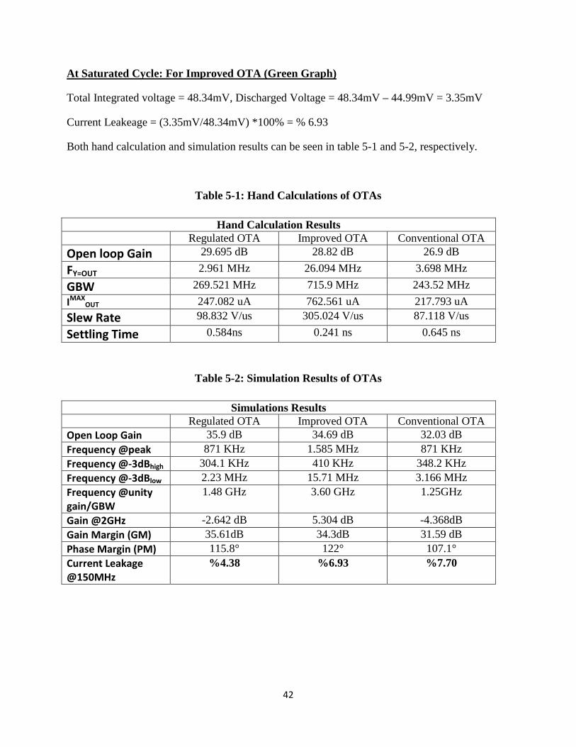
Both hand calculation and simulation results can be seen in table 5-1 and 5-2, respectively.
Table 5-1: Hand Calculations of OTAs
Hand Calculation Results Regulated OTA Improved OTA Conventional OTA Open loop Gain 29.695 dB 28.82 dB 26.9 dB
FY=OUT 2.961 MHz 26.094 MHz 3.698 MHz
GBW 269.521 MHz 715.9 MHz 243.52 MHz IMAX
OUT 247.082 uA 762.561 uA 217.793 uA Slew Rate 98.832 V/us 305.024 V/us 87.118 V/us
Settling Time 0.584ns 0.241 ns 0.645 ns
Table 5-2: Simulation Results of OTAs
Simulations Results Regulated OTA Improved OTA Conventional OTA Open Loop Gain 35.9 dB 34.69 dB 32.03 dB Frequency @peak 871 KHz 1.585 MHz 871 KHz Frequency @-3dBhigh 304.1 KHz 410 KHz 348.2 KHz Frequency @-3dBlow 2.23 MHz 15.71 MHz 3.166 MHz Frequency @unity gain/GBW
1.48 GHz 3.60 GHz 1.25GHz
Gain @2GHz -2.642 dB 5.304 dB -4.368dB Gain Margin (GM) 35.61dB 34.3dB 31.59 dB Phase Margin (PM) 115.8° 122° 107.1° Current Leakage @150MHz
%4.38 %6.93 %7.70
43
CHAPTER 6
CONCLUSION
6.1 Summary
In this thesis work, integrator block for UWB-IR Receiver has been proposed. To understand
current leakage response which occurs during integration, different Operational
Transconductance Amplifier’s characterization parameters such as slew rate, dc gain, cutoff
frequency, GBW and output resistance has been investigated both in system level and transistor
level. Three different OTAs whose names are Conventional Telescopic OTA, Improved
Telescopic OTA and Regulated Telescopic OTA are designed in transistor level with 90 nm
CMOS Technology using 1V supply voltage. Consequently, thanks to higher open loop gain 35.9
dB, lower cutoff frequency 2.3MHz and higher output resistance value Regulated OTA has % 56
improved current leakage responses at 150MHz input signal during discharging than
Conventional Telescopic OTA which has 32.03 dB open loop gain, 3.2 MHz cutoff frequency
and lower output resistance value. Improved Telescopic OTA has % 9 improved current leakage
responses than Conventional Telescopic OTA too with its 34.69 dB open loop gain and 15.71
MHz cutoff frequency.
6.2 Future Work
To obtain lower current leakage response, Operational Transconductance Amplifier should be
designed with sub-threshold transistors so lower cutoff frequencies with higher output resistance
can be gotten with higher dc gain.
Also, transistor level design should be completed for the layout of the entire integrator.
Furthermore, when it is implemented, even two CMOS transistors with the same dimension could
not be identical after fabrication. To obtain more realistic performance of integrator, Monte Carlo
and process corner simulation needs to be conducted before layout.

44
APPENDIX
DESIGN CALCULATIONS

45
Conventional Telescopic OTA
HAND CALCULATION AND SIMULATION RESULTS
Hand Calculation
OPEN LOOP GAIN
|AV | = GM*ROUT where GM = gm1 and
ROUT = { [ [ 1 + (gm3 + gmbs3)*ro3]*ro1 + ro3 } || { [ [ 1 + (gm5 + gmbs5)*ro5]*ro7 + ro5 }
ROUT ≈ (gm3*ro3*ro1) || (gm5*ro5*ro7)
|AV | = gm1 * [(gm3*ro3*ro1) || (gm5*ro5*ro7)] where
Gm1 = 3.87717 m, gm3 = 3.88647m, gm5 = 4.64024m , ro1 = 1.69599K + 50K = 51.69599K ,
Ro3 = 390.851 , ro5 = 1.26483K , ro7 = 1.04951K,
As a Result |AV | = 22.1428, 20log |AV |= 26.9 dB
AC ANALYSIS (Hand Calculation)
For 1st pole A
Wp,A = 1
𝑅𝑠[(𝐶𝐺𝑆1+𝐶𝑖𝑛)+�1+ 𝑔𝑚1𝑔𝑚3+𝑔𝑚𝑏3�𝐶𝐺𝐷1]
where
Rs = 50K, gm1 = 3.87717m, gm3 = 3.88647m, gmbs3 = 500.638u,
CGS1 = 51.6542f, CGD1 = 11.5638f, Cin = 5pF
As a result fA = 627.362 KHz
For 2nd pole X
Wp,X = 𝑔𝑚3+𝑔𝑚𝑏32𝐶𝐺𝐷1+𝐶𝐷𝐵1+𝐶𝑆𝐵3+𝐶𝐺𝑆3
where
gm3 = 3.88647m, gmbs3 = 500.638u,
CDB1 =2.37541f, CGD1 = 11.5638f, CSB3 = 5.30924f, CGS3 = 77.4536f
As a result fX = 6.448 GHz

46
For 3rd pole Y
Wp,out = 1𝑅𝑜𝑢𝑡(𝐶𝐷𝐵3+𝐶𝐺𝐷3+𝐶𝐿+𝐶𝑠)
where
ROUT = (gm3*ro3*ro1) || (gm5*ro5*ro7), CDB3 = 4.3121f, CGD3 = 29.999f, CL = 2.5p,Cs = 5pF
Gm5 = 4.64024m, ro5 = 1.26483K, ro7 = 1.04951K gm3 = 3.88647m,
Ro3 = 390.851, ro1 = 1.69599K + 50K = 51.69599K
As a result fY = 3.698 MHz
GAIN BANDWIDTH PRODUCT
GBW = 𝑔𝑚12𝜋(𝐶𝐷𝐵3+𝐶𝐿+𝐶𝐺𝐷3)
where
gm1 = 3.87717m and CL = 2.5pF, CDB3 = 4.3121f, CGD3 = 29.999f,
As a result GBW = 243.52 MHz
MAXIMUM OUTPUT CURRENT
IOUT MAX = I BIAS /2 where IBIAS = 435.586u
As a result IMAXOUT = 217.793uA
SLEW RATE AND SETTLING TIME
SR = IOUT MAX 𝐶𝐿
where
IMAXOUT = 217.793uA and CL = 2.5pf, Settling Time = CL /gm1
As a Result SR = 87.118 V /us , Settling Time = 0.645ns

47
Improved Telescopic OTA
HAND CALCULATION AND SIMULATION RESULTS
Hand Calculation
OPEN LOOP GAIN
|AV | = GM*ROUT where GM = gm1+gm10 and
ROUT ≈ (gm3*ro3*(ro1||ro10)) || (gm5*ro5*ro7)
|AV | = (gm1+gm10)(gm3*ro3*(ro1||ro10)) || (gm5*ro5*ro7) where
Gm1 = 10.38m, gm10 = 965.685u, gm3 = 11.654m, gm5 = 13.5502m , ro1 = 328.438 + 50K = 50.239K , Ro3 = 331.077 , ro5 = 293.079 , ro7 = 208.349K,
As a Result |AV | = 27.60, 20log |AV |= 28.82 dB
AC ANALYSIS (Hand Calculation)
For 1st pole A
Wp,A = 1
𝑅𝑠[(𝐶𝐺𝑆1+𝐶𝑖𝑛)+�1+𝑔𝑚1+𝑔𝑚10𝑔𝑚3+𝑔𝑚𝑏3�𝐶𝐺𝐷1]
where
Rs = 50K, gm1 = 10.38m, gm10 = 965.685u, gm3 = 11.654m, gmbs3 = 1.4758m,
CGS1 = 59.4236f, CGD1 = 11.8364f, Cin = 5pF
As a result fA = 626.410 KHz
For 2nd pole X
Wp,X = 𝑔𝑚3+𝑔𝑚𝑏32𝐶𝐺𝐷1+𝐶𝐷𝐵1+𝐶𝑆𝐵3+𝐶𝐺𝑆3
where
gm3 = 11.654m, , gmbs3 = 1.4758m,
CDB1 =2.78277f, CGD1 = 11.8364f, CSB3 = 5.57967f, CGS3 = 91.9886f
As a result fX = 16.849 GHz
48
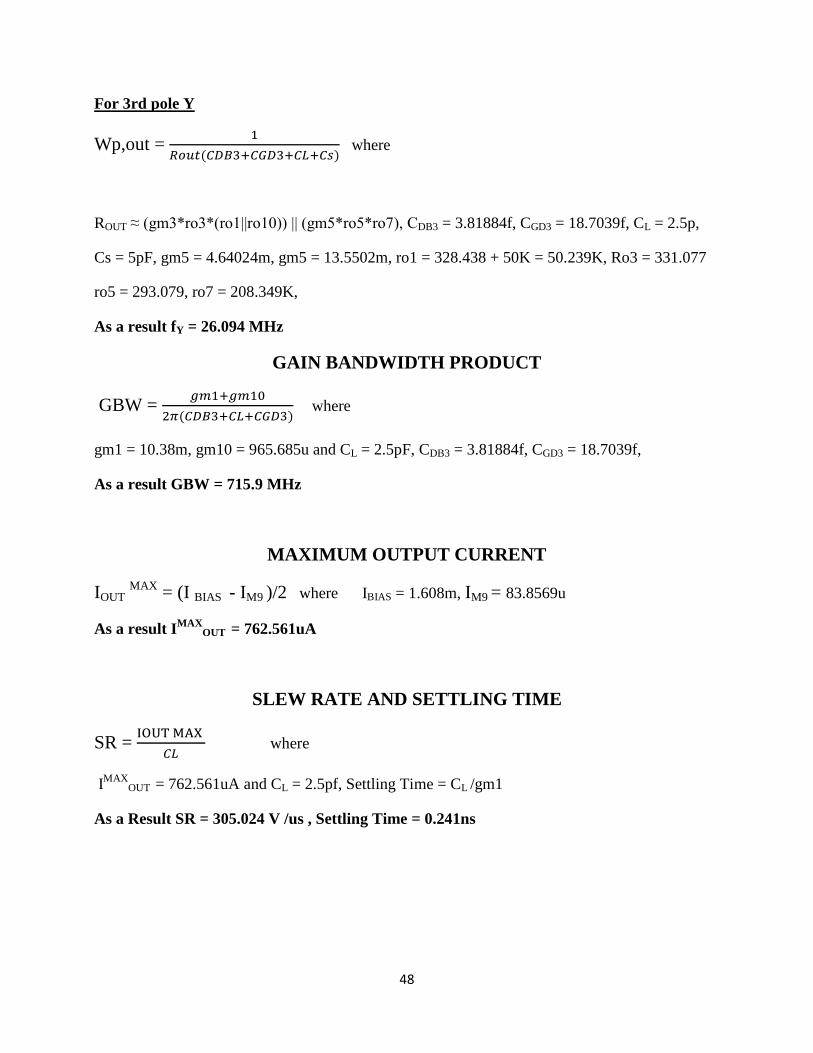
For 3rd pole Y
Wp,out = 1𝑅𝑜𝑢𝑡(𝐶𝐷𝐵3+𝐶𝐺𝐷3+𝐶𝐿+𝐶𝑠)
where
ROUT ≈ (gm3*ro3*(ro1||ro10)) || (gm5*ro5*ro7), CDB3 = 3.81884f, CGD3 = 18.7039f, CL = 2.5p,
Cs = 5pF, gm5 = 4.64024m, gm5 = 13.5502m, ro1 = 328.438 + 50K = 50.239K, Ro3 = 331.077
ro5 = 293.079, ro7 = 208.349K,
As a result fY = 26.094 MHz
GAIN BANDWIDTH PRODUCT
GBW = 𝑔𝑚1+𝑔𝑚102𝜋(𝐶𝐷𝐵3+𝐶𝐿+𝐶𝐺𝐷3)
where
gm1 = 10.38m, gm10 = 965.685u and CL = 2.5pF, CDB3 = 3.81884f, CGD3 = 18.7039f,
As a result GBW = 715.9 MHz
MAXIMUM OUTPUT CURRENT
IOUT MAX = (I BIAS - IM9 )/2 where IBIAS = 1.608m, IM9 = 83.8569u
As a result IMAXOUT = 762.561uA
SLEW RATE AND SETTLING TIME
SR = IOUT MAX 𝐶𝐿
where
IMAXOUT = 762.561uA and CL = 2.5pf, Settling Time = CL /gm1
As a Result SR = 305.024 V /us , Settling Time = 0.241ns

49
Regulated Cascode OTA
HAND CALCULATION AND SIMULATION RESULTS
Hand Calculation
OPEN LOOP GAIN
|AV | = GM*ROUT where GM = gm1 and
ROUT ≈ ((gm3+gm10)*ro3*(ro10||ro9)*ro1) || (gm5*ro5*ro7)
|AV | = gm1((gm3+gm10)*ro3*(ro10||ro9)*ro1) || (gm5*ro5*ro7)
Gm1 = 4.27427m, gm10 = 1.171m, gm3 = 4.5512m, gm5 = 5.20223m, ro1 = 949.328 + 50K = 50.949K, Ro3 = 700.928, ro5 = 1.68978K, ro7 = 587.081, ro9 = 3.12956K, ro10 = 15.055K
As a result |AV | = 30.53, 20log |AV |= 29.695 dB
AC ANALYSIS (Hand Calculation)
For 1st pole A
Wp,A = 1
𝑅𝑠[(𝐶𝐺𝑆1+𝐶𝑖𝑛)+�1+ 𝑔𝑚1𝑔𝑚3+𝑔𝑚10+𝑔𝑚𝑏3�𝐶𝐺𝐷1]
Rs = 50K, gm1 = 4.27427m, gm10 = 1.171m, gm3 = 4.5512m, gmbs3 =605.101u,
CGS1 = 59.4236f, CGD1 = 11.8364f, Cin = 5pF
As a result fA = 627.51 KHz
For 2nd pole X
Wp,X = 𝑔𝑚3+𝑔𝑚𝑏32𝐶𝐺𝐷1+𝐶𝐷𝐵1+𝐶𝑆𝐵3+𝐶𝐺𝑆3
where
gm3 = 4.5512m, gmbs3 =605.101u,
CDB1 =2.52967f, CGD1 = 11.8364f, CSB3 = 5.15759f, CGS3 = 81.5152f
As a result fX = 7.27 GHz
50
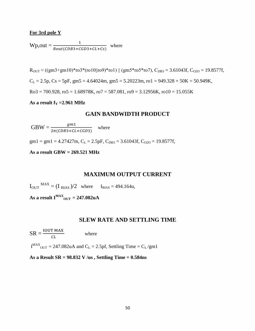
For 3rd pole Y
Wp,out = 1𝑅𝑜𝑢𝑡(𝐶𝐷𝐵3+𝐶𝐺𝐷3+𝐶𝐿+𝐶𝑠)
where
ROUT ≈ ((gm3+gm10)*ro3*(ro10||ro9)*ro1) || (gm5*ro5*ro7), CDB3 = 3.61043f, CGD3 = 19.8577f,
CL = 2.5p, Cs = 5pF, gm5 = 4.64024m, gm5 = 5.20223m, ro1 = 949.328 + 50K = 50.949K,
Ro3 = 700.928, ro5 = 1.68978K, ro7 = 587.081, ro9 = 3.12956K, ro10 = 15.055K
As a result fY =2.961 MHz
GAIN BANDWIDTH PRODUCT
GBW = 𝑔𝑚12𝜋(𝐶𝐷𝐵3+𝐶𝐿+𝐶𝐺𝐷3)
where
gm1 = gm1 = 4.27427m, CL = 2.5pF, CDB3 = 3.61043f, CGD3 = 19.8577f,
As a result GBW = 269.521 MHz
MAXIMUM OUTPUT CURRENT
IOUT MAX = (I BIAS )/2 where IBIAS = 494.164u,
As a result IMAXOUT = 247.082uA
SLEW RATE AND SETTLING TIME
SR = IOUT MAX 𝐶𝐿
where
IMAXOUT = 247.082uA and CL = 2.5pf, Settling Time = CL /gm1
As a Result SR = 98.832 V /us , Settling Time = 0.584ns
51
REFERENCES
[1] M. Camus, B. Butaye, L. Garcia, M. Sie, B. Pellat, and T. Parra, “A 5.4mW/0.07mm2
2.4GHz front-end receiver in 90nm CMOS for IEEE 802.15.4 WPAN standard”, IEEE J.
Solid-State Circuits, vol. 43, no. 6, pp. 1372-1383, Jun. 2008.
[2] Mahim Ranjan, Lawrance Larson, “A low-cost and low-power CMOS receiver front-end
for MB-OFMD ultra-wideband systems”, IEEE J. Solid-State Circuits, vol. 42, no. 3, pp.
592-601, Mar. 2007.
[3] David Sarmiento M., Zhuo Zou, Qin Zhou, Jia Mao, Peng Wang, Fredrik Jonsson, Li-
Rong Zheng, “Analog Front-End RX Design for UWB Impulse Radio in 90nm CMOS”,
IEEE,pp.1552, 2011.
[4] M. Cheol Ha, Y. Jin Park, and Y. Seong Eo, “ A 3-5GHz Non-Coherent IR-UWB
Receiver”, Journal of Semiconductor Technology and Science, Vol. 8, No. 4, December
2008.
[5] H. Arslan, Z.Chen, and M. Benedetto,” Ultra-wideband Wireless Communication”, Wiley
Interscience, Hoboken, New Jersey, 2006.
[6] Stoica Lucian, “Non-Coherent Energy Detection Transceivers for Ultra Wideband
Impulse Radio Systems”, Universitatis Ouluensis, Oulu, 2008.
[7] S. Vitavasiri, “A Non Coherent Ultra-Wideband Receiver: Algorithms and Digital
Implementation”, Massachusetts Institute of Technology, May 2007.
[8] A. Michael Orndorff, “Transceiver Design for Ultra Wideband Communications”,
Virginia Polytechnic Institute and State University, May 20, 2004.
[9] A.Vouilloz, M.Declercq, and C.Dehollain, and P. Deval, “A 2V 600uA, 1 GHz, BiCMOS,
super-regenerative receiver at 1 GHz”, IEEE J. Solid-State Circuits. Vol. 36 no. 3, pp.
452-466, March 2011.
52
[10] Y. Tong, Y.Zheng, Yong-Ping Xu, ”A coherent ultra-wideband receiver IC system for
WPAN application”, in IEEE International Conference on Ultra-wideband, pp. 60-64,
2005.
[11] Tiuraniemi, S., Stoica, L.; Rabbachin, A., and Oppermann, I., “Front-end receiver for low
power, low complexity non-coherent UWB communication system,” IEEE International
Conference on Ultra- Wideband, pp. 339-343, Sept. 2005.
[12] Yuanjin Zheng, Yan Tong, Jiangnan Yan; Yong- Ping Xu, Wooi Gan Yeoh, and Fujiang
Lin, “A low power non-coherent CMOS UWB transceiver ICs,” IEEE Radio Frequency
Integrated Circuits (RFIC) Symposium, Digest of Papers, pp. 347-350, June 2005.
[13] Fredrik Johnson, Jia Mao, “UWB Receiver System Design Specification”, Ipack Vinn
Excellence Center, KTH, pp.5, August 2009.
[14] Majid Baghaei-Nejad, D.Sarmiento Mendoza, Zhuo Zou, Soheil Radiom, Georges Gielen,
Li-Rong Zheng, Hannu Tenhunen, “A Remote-Powered RFID Tag with 10Mb/s UWB
Uplink and -18.5dBm-Sensitivity UHF Downlink in 0.18um CMOS”, IEEE International
Solid-State Circuit Conference ISSCC, 2009.
[15] M. Adnan Al-Alaoui, “A Novel Approach to Designing a Noninverting Integrator with
Built-in low Frequency Stability High Frequency Compensation and High Q” , IEEE
Transactions on Instrumentation and Measurement, Vol. 38. No. 6, December 1989.
[16] Electronics Tutorials, “Passive Low Pass Filter”, http://www.electronics-
tutorials.ws/filter/filter_2.html, 12-30-2011.
[17] W.J.A Heij, E. Seevinck, and K. Hoen, “Practical Formulation of the Relation Between
Filter Specification and The Requirements for the Integrator Circuits”, IEEE Transaction
on Circuits and Systems, Vol. 36, No.8, August 1989.
[18] S.Pavan and Y.Tsividis, “High Frequency Continuous Time Filter in Digital CMOC
Processes”, Springer Link, DOI: 10.1007/0-300-6-47014-4_3, pp. 33-69, 2002
[19] S.Rehman, “ Survey of Analog Design Challenges in Gm-C Integrator for Continous
Time Low Pass Modulator”, National Science and Technology, Islamabad, Pakistan
53
[20] Willy M.C. Sansen, “Analog Design Essentials”, Catholic University, Leuven, Belgium,
Springer Publisher, Netherland, pp. 33, 2006.
[21] Behzad Razavi, “Design of Analog CMOS Integrated Circuits”, University of California,
Los Angeles, Mc GRAW-Hill Intenational Edition, pp. 185.
[22] E.Säckinger and W.Guggenbuhl, “A High Swing, High Impedance MOS Cascode
Circuit”, IEEE Journal of Solid-State Circuits, Vol. 25, No.1, February 1990.
[23] G. F. Ross, “Transmission and reception system for generating and receiving base-band
duration pulse signals without distortion for short base-band pulse communication system,”
US Patent 3,728,632, April 17, 1973.
[24] C.Duan, P.Orlik, Z.Sahinoglu, and F.Molisch,” A Non-Coherent 802.15.4a UWB Impulse
Radio” Mutsubishi Electric Research Laboratories, September, 2007.