design of a multiband microstrip differential phase ... · 2-6 phase shifter designs ......
TRANSCRIPT
Design of a Multiband Microstrip
Differential Phase Shifter for Wireless Systems
Ali Reza Aboofazeli
A thesis presented to Ottawa-Carleton Institute for
Electrical and Computer Engineering
in partial fulfillment to the thesis requirement for the degree of
MASTER OF APPLIED SCIENCE
in
ELECTRICAL ENGINEERING
University of Ottawa
Ottawa, Ontario, Canada
October 2016
© Ali Reza Aboofazeli, Ottawa, Canada, 2016

ii
Abstract
This thesis investigated the design of a compact multiband differential reflective phase
shifter based on slot-coupled coupler layout. Such phase shifter configuration is formed
of a hybrid coupler with the coupled and transmission ports ended with elliptically
shaped microstrip loads. By optimizing the ending ports of the coupler, we achieved a
1.2-6.0 GHz differential phase from - 90o to + 90o, a frequency range that covers most
commercial, satellite and personal mobile communication bands.
Furthermore, we can obtain different phase ranges by terminating the coupler with
suitable reactance loads. Indeed, the simulations showed that the proposed design can
achieve ± 30o, ± 45o, and ± 90o differential phase shifts with deviation less than 3o, as
well as return loss and insertion loss better than 10 dB and 1 dB, respectively. The total
size of the designed phase shifter is 25 x 60 mm2. Measurements results agreed well
with the simulations, thus demonstrating the proposed design approach.

iii
Acknowledgments
I would first like to thank my supervisor Professor Mustapha C.E. Yagoub who has
supported me throughout my thesis with his patience and knowledge.
I attribute the level of my Master’s degree to his encouragement and effort and without
him this thesis, too, would not have been completed or written. One simply could not
wish for a better or friendlier supervisor.
Last but the most I would like to thank my family and my friends for their support and
encouragements during this thesis work.
iv
Abstract ......................................................................................................... ii
List of variables ........................................................................................... ix
List of Acronyms .......................................................................................... x
Chapter One ................................................................................................. 1
Introduction .................................................................................................. 11-1 Motivations .............................................................................................................. 11-2 Thesis contributions ............................................................................................... 31-3 Thesis Organization ............................................................................................... 3
Chapter Two ................................................................................................. 4
Phase Shifters Review .................................................................................. 42-1 Definitions ...................................................................................................................... 42-2 Design Parameters ........................................................................................................ 52-3 Different Types of Phase Shifters ................................................................................ 62-4 Phase Shifters Design Topologies ................................................................................ 9
2-4-1 switched line phase shifters ..................................................................................... 92-4-2 Hybrid-coupled phase shifter ................................................................................ 102-4-3 Loaded-line phase shifters ..................................................................................... 102-4-4 High-pass-low-pass phase shifters ........................................................................ 112-4-5 Discussion .............................................................................................................. 12
2-5 Planar Couplers ........................................................................................................... 132-5-1 Edge coupling configuration ................................................................................. 142-5-2 Broadside slot coupling configuration ................................................................... 14
2-6 Phase Shifter Designs .................................................................................................. 152-6-1 Schifman’s phase shifter ........................................................................................ 162-6-2 Mosko-Shelton’s constant phase shifter and directional coupler .......................... 172-6-3 Abbosh wideband phase shifter ............................................................................. 20
2-7 Conclusions .................................................................................................................. 22
Chapter Three ............................................................................................ 24
Coupler Design ........................................................................................... 243-1 Design Approach ......................................................................................................... 24
3-1-1 Odd and even mode analysis ................................................................................. 26

v
3-1-2 Coupler analytical formulation .............................................................................. 273-2 Designing the hybrid coupler ..................................................................................... 323-3 Manufactured coupler ................................................................................................ 353-3 Conclusion .................................................................................................................... 37
Chapter Four .............................................................................................. 38
Differential Phase Shifter Design ............................................................. 384-1 Designing the differential reflective phase shifter .................................................... 38
4-1-1 Theoretical approach ............................................................................................. 384-1-2 Differential reflective phase shifter’s formulation ................................................ 41
4-2 Design Results with Elliptical-Shaped Microstrip Load ......................................... 424-3 Parametric Analysis .................................................................................................... 464-4 Manufacture and Test Results of the 45o Differential Phase Shifter ...................... 484-5 comparison of the designed phase shifter with others ............................................. 514-6 Conclusion .................................................................................................................... 54
Chapter 5 .................................................................................................... 55
Conclusions and future works .................................................................. 555.1 Conclusions .................................................................................................................. 555.2 Future works ................................................................................................................ 56
References ................................................................................................... 57

vi
Table of Figures
Figure 2 - 1. Different electronically phase shifters [14]. ............................................. 7Figure 2 - 2 PIN diode I-V characteristics [15] ............................................................ 8Figure 2 - 3. PIN diode phase shifters can shift the phase with switching signal between
two paths with two different lengths l0, l0 + l . [15] ............................................ 8Figure 2 - 4. Switched line phase shifters [14]. .......................................................... 10Figure 2 - 5. Hybrid-coupled phase shifters [14] ........................................................ 11Figure 2 - 6. High-pass-low-pass phase shifter [21] ................................................... 12Figure 2 - 7. an edge-coupled configuration [26] ....................................................... 14Figure 2 - 8. Slot coupling configuration [28] ............................................................ 15Figure 2 - 9. Error-correcting network and its two possible differential phase responses
[38]. ..................................................................................................................... 18Figure 2 - 10. Type-B network and its differential phase response. ........................... 19Figure 2 - 11. Configuration of multi-section directional coupler. a) required coupling
response of multi-section coupler. b) decomposition of coupling response ....... 20Figure 2 - 12. Phase shifter a) upper layer b) middle layer c) lower layer d) whole
structure [40] ....................................................................................................... 21Figure 2 - 13 Phase shifter as a four-port device with two open-circuit ports [40] .... 21
Figure 3 - 1. General structure of Tanaka coupler with plane coupling a) transmission
lines, gap and sub layers’ arrangement b) upper view of coupler c) odd and even
modes equivalent circuit [42] .............................................................................. 25Figure 3 - 2. Offered coupler structure’s layers with plane coupling ........................ 26Figure 3 - 3. The coupler model for semi-static analysis [42] ................................... 28Figure 3 - 4. Conversions to find unit capacitor of coupler’s even mode ................. 29Figure 3 - 5. the offered wideband structure layers in 1.2-6 GHz frequency band with
plane coupling ..................................................................................................... 33Figure 3 - 6.Simulation results of the hybrid coupler in 1.2-6 GHz frequency band a)
reflective coefficients b) transmission coefficients c) phase shift d) phase and
amplitude unbalance. .......................................................................................... 35
vii
Figure 3 - 7. the manufactured coupler measurement results. ................................... 35
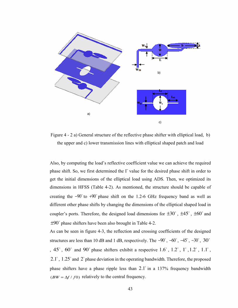
Figure 4 - 1 Schematic version of offered reflective phase shifter by using the loaded
symmetric directional coupler ............................................................................. 42Figure 4 - 2 a) General structure of the reflective phase shifter with elliptical load, b)
the upper and c) lower transmission lines with elliptical shaped patch and load 43Figure 4 - 3 a) phase shift, b) phase ripple, c) return loss, d) insertion loss of the ±30!
, ±45! , ±60! and ±90! differential phase shifters with elliptical shaped
microstrip load in 1.2-6 GHz frequency band. ................................................... 46Figure 4 - 4 Simulation results of the 45o differential reflective phase shifter for
parametric analysis a) the effect of changing the load’s dimensions on phase shift
b) the effect of changing the length of the reference line on the phase shift c) the
effect of changing the load’s dimensions on the return loss d) the effect of
changing the load’s dimensions on the insertion loss ......................................... 48Figure 4 - 5 a) Measurement system, b) the manufactured 45o phase shifter (top, bottom
and middle views). .............................................................................................. 50Figure 4 - 6 Measurement results of the 45o phase shifter, Return and insertion loss 50Figure 4 - 7 Comparing measurement and simulation results for S11 ......................... 51Figure 4 - 8. Comparing measured and simulated phase shift .................................... 51
viii
Table of Tables
Table 2 - 1 comparison between slot-coupled and edge-coupled configurations [29] 15Table 2 - 2. Comparison between different topologies of phase shifters .................... 23
Table 3 - 1 Dimensions of the designed coupler in 1.2-6 GHz frequency band. ........ 33Table 3 - 2 Comparison of the designed coupler characteristics vs. existing published
works. .................................................................................................................. 36
Table 4- 1 Designed coupler dimensions for reflective phase shifter ......................... 42Table 4- 2 Dimensions of the designed elliptical shaped load to get the ±30! , ±45! ,
±60! and ±90! phase shifts ................................................................................ 44Table 4- 3 Comparison of the designed phase shifter’s specification with other phase
shifters with different structures ......................................................................... 52

ix
List of variables
% Phase constant
βef Effective phase constant
Γ Reflection coefficient
&'(( Effective permittivity
) Electrical length of a uniform line
* Wavelength
+ Phase
, Angular frequency
b Reflective waves
CTe Total unit capacitor of even mode
CTo Total unit capacitor of odd mode
IL Insertion loss
- Length
lref Reference line length
L Length of patch
LS Length of gap
RL Return loss
S Scattering parameters
W Width of patch
Ws Width of gap
./ Characteristic impedance
Z0e Characteristic impedance in even-mode
Z0o Characteristic impedance in odd-mode

x
List of Acronyms
ADS Advanced Design Systems Software
BW Bandwidth
DCS Digital Communication systems
DGS Defected Ground Structure
GPS Global Positioning System
MEMS Micro-electromechanical systems
MMIC Monolithic Microwave Integrated Circuit
PCS Personal Communication Systems
S-DMB Satellite-Digital Multimedia Broadcasting
SIW Substrates Integrated Waveguide
UMTS Universal Mobile Telecommunications Systems
WiMax Worldwide Interoperability for Microwave Access
WLAN Wireless Local Area Network

1
Chapter One
Introduction
1-1 Motivations In modern communication systems, there is a need to control the direction of signal
radiation in order to improve its properties in a particular direction. This is called beam
steering [1].
To this aim, phase shifters introduce a configured amount of time delay (or phase at a
certain frequency) in the signal passing through it; the amplitude of the radiated signal
in each lobe is being controlled by a Variable Gain Amplifier. The radiated waves
interact with each other either destructively or constructively. Therefore, by adjusting
the phases and amplitudes of the transmitted signals, it is possible to reduce the
radiation in all unwanted directions (by destructive interaction) while increasing it in a
particular direction (by constructive interaction) [1]- [3].
Phase shifters are then a critical component in many RF and microwave systems.
Applications include controlling the relative phase of each element in a phase array
antenna in a radar or a steerable communication link, and in cancelation loops used in
high linearity amplifiers.
Because of their importance in communication systems, a quite impressive number of
researches have been already published regarding their design while many others are
still ongoing to enhance the phase shifter characteristics such as increasing bandwidth,
decreasing ripple phase, reducing size, and/or decreasing losses, to name a few.
Depending on how to control the phase shift, phase shifters can be categorized into two
main groups: mechanical and electronical, the latter being much popular, especially in

2
phase array antennas [1]. Because of the ever-increased need for efficient integrated
communication systems with wider bandwidth, the objective of the present work was
to design integrated phase shifters with wide bandwidth and minimum attenuation.
In this optic, features such as flexibility, availability, and ease to use, have made
wireless communication systems unavoidable components in our professional as well
as personnel life.
We have then focused in this work on the design of a multiband 1.2-6.0 GHz phase
shifter, i.e., a frequency range that covers most commercial, satellite and personal
mobile communication bands such as Global Positioning System (GPS, 1.575 GHz),
Digital Cellular System (DCS, 1710 - 1880 GHz), Personal Communications Service
(PCS, 1850- 1990 MHz), Universal Mobile Telecommunications System (UMTS,
1900-2200 MHz), Wireless Broadband (WiBro, 2300 - 2390 MHz), Bluetooth (2.4
GHz), Wireless Local Area Network (WLAN, 5.1–5.9 GHz), and Worldwide
Interoperability for Microwave Access (WiMAX, 2.5 and 5.8 GHz).
Slot-coupled structures are a good candidate for wideband applications because of their
tight coupling, low phase deviation and reduced size [4]. In addition, among integrated
phase shifters, microstrip differential phase shifter are widely used in modern
communication systems [4]-[10]. In fact, such phase shifters have broad applications
in microwave circuits such as butler matrices, monopulse networks, beam-scanning
phased arrays, microwave instrumentation and measurement systems, modulators and
many other industrial applications. They can provide suitable phase difference between
two different paths with minimum effect on each other.
Wideband differential phase shifters are mainly based on the design proposed by
Schiffman [6], an edge-coupled stripline transmission configuration. This structure
consists of a reference line and two edge-coupled striplines integrated together at their
bottom. By choosing the proper length of these lines and the coupling, the phase
difference between them can be made constant over one octave frequency band.
However, a very narrow gap between the edge-coupled lines is needed for a broadband
performance and when this circuit is fabricated in microstrip technology, its operation
decreased. So, Abbosh [4] proposed a microstrip-slot-microstrip coupler with an
elliptical-shaped broadside coupled structure that shows good wideband properties.

3
1-2 Thesis contributions
In this thesis, the main contribution has been to propose a modified configuration of
Abbosh’s phase shifter [4] that can operate over a quite wideband range, covering the
1.2-6.0 GHz band. The proposed enhancements allowed to successfully complete the
design of a coupler with suitable characteristic such as 3 dB coupling with minimum
return loss, phase imbalance and amplitude imbalance and also the design of a phase
shifter with high performance in the targeted frequency range, i.e., 137% bandwidth,
((f2-f1)/fc) maximum of 3o phase deviation, as well as return and insertion loss better
than 10 dB and 1 dB, respectively.
1-3 Thesis Organization
This thesis is divided into four chapters. After this introductory chapter, the following
chapter presents an overview of the existing phase shifters types, designs and
requirements.
In the third chapter, the design process of a wideband directional hybrid coupler is
described including the odd and even modes analysis and related simulations.
Chapter Four provides the design, implementation and results of the multiband
differential reflective phase shifter. Simulations were performed using both a circuit
simulator (Advanced Design System - ADS, from Keysight Technologies) and a full-
wave electromagnetic solver (High-Frequency-Simulation-Software – HFSS, from
ANSYS). The results for phase ripple, phase shift are shown and compared to other
works. The manufactured test results for this phase shifter have been brought in this
chapter as well.

4
Chapter Two
Phase Shifters Review
In this chapter, we will first review the different topologies of phase shifters, depicting
the advantages and disadvantages of each structure. This step will allow us selecting
the most suitable for the targeted application.
2-1 Definitions
Phase shifters are used to change the transmission phase angle (i.e., the phase of the
S21 parameter) of a network. Ideal phase shifters provide low insertion loss and equal
amplitude (loss) in all phase states. Most phase shifters are passive reciprocal networks,
meaning that they work effectively on signals passing in either direction [11].
While the applications of microwave phase shifters are numerous, perhaps the most
important is within a phased array antenna system (as known as Electrically Steerable
Array, or ESA), in which the phase of a large number of radiating elements are
controlled to force the electro-magnetic (EM) wave to add up at a particular angle to
the array. For this very purpose, phase shifters are often embedded in TR modules [11].
The total phase variation of a phase shifter needs only be 360o to control an ESA of
moderate bandwidth. Networks that stretch phase more than 360o are often called time
delay bits or true time delays (part of a time delay unit or TDU), and are built similar
to the switched line phase shifters that will be described below [11].
5
2-2 Design Parameters
In recent decades, one of the most important applications of phase shifters is in phase
array structures. In antenna theory, a phased array is an array of antennas in which the
relative phases of the respective signals feeding the antennas are set in such a way that
the effective radiation pattern of the array is reinforced in a desired direction and
suppressed in undesired directions. The phase relationships among the antennas may
be fixed, as in a tower array, or may be adjustable, as for beam steering.
Common phase arrays can have up to thousands radiation elements. In these structures,
phase shifters are in the form of constant time delay or phase delay devices [12].
Because of this, phase array structures are in the form of phase scanning and time-delay
scan. Phase shifters with small loss, low handling power, continuous adjusting
capability and low production costs are among the most fundamental phase array
antennas part that direct EM waves with electronically controlling the signal’s phase
while antenna is not physically moving.
In designing a phase shifter, beside cost and tolerances (which we did not consider in
this work), different design parameters have to be considered:
• Insertion Loss: The insertion loss of a phase shifter is largely driven by the
number of stages needed and the operating frequency. 4-6dB is a typical range
for a design with 360o of control. The variation with frequency at a given phase
is also critical and performance of +/-1dB over an octave bandwidth is often
required [13].
• Amplitude Imbalance: The magnitude of the RF signal should not be affected by
the phase shifter in ideal conditions. In practice, variations are expected in the
amplitude of the RF signal over frequency, resulting in unequal distribution of
amplitude during the beam steering of the antenna [13].
• Return Loss: Return loss is a measure of the input impedance matching of the
phase shifter. A typical number for a broadband device would be –10dB to –15dB
[13].

6
• Transmission coefficient: In telecommunications, the transmission coefficient is
the ratio of the amplitude of the complex transmitted wave to that of the incident
wave at a given point in a transmission chain.
• Phase deviation: In phase modulation, the phase deviation is stated as the
maximum difference between the instantaneous phase angle of the modulated
wave and the phase angle of the unmodulated carrier.
• Size: Size could be an important issue depending on the application as well as
other requirements. However, covering a smaller place is always desired to make
room for other components in a system.
• Power Handling Capability: Although power-handling capability of the phase
shifter depends on the application, it can be a very important property in
designing the system. Especially in transmitter mode of phased array radars,
phase shifters must be capable of handling much power. However, generally each
phase shifter in the array is required to handle some portion of the total power
since transmitter power is distributed among all the phase shifters [12].
2-3 Different Types of Phase Shifters
In general, phase shifters can be categorized into three groups: Ferrite, Semiconductors
and Bulk Semiconductors. Figure 2.1 shows different common categories of
electronically phase shifters, in which semiconductor-based ones are the most
important [13].
In fact, although Ferrites phase shifters have less input loss, they are complex and
expensive. Also they require manual adjusting and have high consumption power [14].
Bulk semiconductor phase shifters are cheaper and smaller but they have limited
applications because of high input loss in high frequencies. Also they cannot exhibit
continuous phase shift [14].

7
Figure 2 - 1. Different electronically phase shifters [14].
Semiconductor-based phase shifters can be classified as analog or digital. Analog phase
shifters provide a continuously variable phase, usually controlled by a voltage [13],
while digital phase shifters provide a discrete set of phase states that are controlled by
two-state "phase bits." The highest order bit is 180o, the next highest is 90o, then 45o,
etc., as 360o is divided into smaller and smaller binary steps. A three-bit phase shifter
would have a 45o Least Significant Bit (LSB), while a six-bit phase shifter would have
a 5.6o least significant bit. Most phase shifters are of the digital variety, as they are
more immune to noise on their voltage control lines.
Considering a semiconductor controlling element as a switch, phase shifters are usually
based on PIN diodes or FETs. A PIN diode is a P-N junction with a large depletion
region rather than normal diode (Figure 2-2 [15]). Adding this intrinsic region will help
controlling the conductance capability in forward bias and also decreasing capacitor in

8
reverse bias. In fact, in forward bias, resistance in signal path will become negligible
while decreasing capacitor in reverse bias will lead to higher impedance in this track.
Figure 2 - 2 PIN diode I-V characteristics [15]
Therefore, PIN diode phase shifters can shift the phase with switching signal between
two paths with two different lengths -/, -/01 (Figure 2.3 [15]).
Figure 2 - 3. PIN diode phase shifters can shift the phase with switching signal
between two paths with two different lengths -/, -/01 . [15]
Phase shift is proportional to extra path delay %-, where % is the mean propagation
constant and l the difference between lengths.
FET phase shifter is used as a two-terminal switch controlled by the gate voltage and
has many advantages compared to PIN diode [15]. It has higher switching speed and
9
less consumption power. While PIN diode is known as a digital shifter, FET can operate
in both analog and digital modes. Note that since semiconductor phase shifters are
expensive and have high input loss in microwave frequencies, new technologies are
using narrowband linear dielectrics and Micro-Electro-Mechanical Systems (MEMS)
to obtain phase shifts with very low input loss (< 2dB).
2-4 Phase Shifters Design Topologies
2-4-1 switched line phase shifters
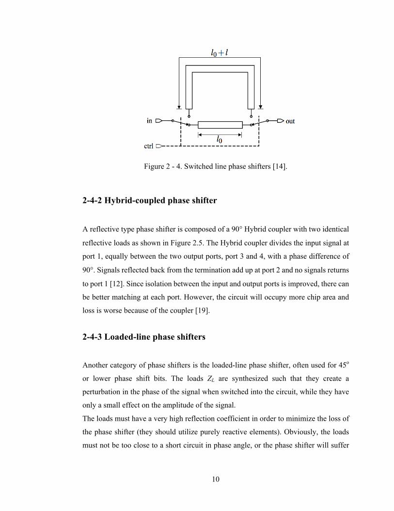
The primary kind of phase shifters is the switched-line phase shifter. With this kind of
phase shifter, it is conceivable to switch between two (or more) delay lines as shown
in Figure 2-4. The phase shift given by this circuit is the distinction between electrical
lengths between two transmission lines.
There are certain disadvantages for this type. First, an advanced CMOS technology is
expected to realize this phase shifter at high frequencies with low insertion loss.
Second, the two lines have unequal lengths and different attenuations. This implies that
the two lines that the two-time delay states will have different attenuations, resulting in
amplitude imbalance between the two states. Third, to realize large time delays, long
line lengths are needed which is impractical for integrated circuit realization for most
frequency ranges and increases loss for larger time delays [17].
10
Figure 2 - 4. Switched line phase shifters [14].
2-4-2 Hybrid-coupled phase shifter
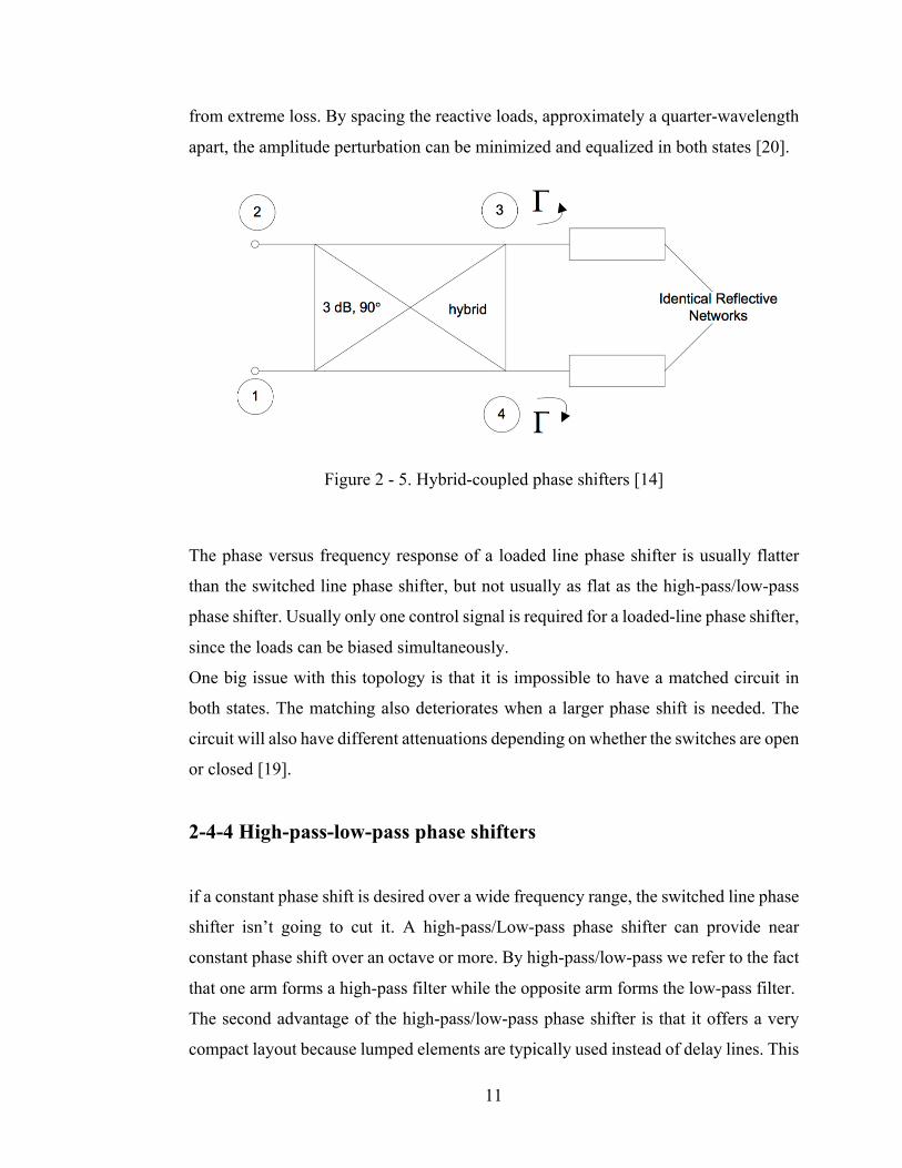
A reflective type phase shifter is composed of a 90° Hybrid coupler with two identical
reflective loads as shown in Figure 2.5. The Hybrid coupler divides the input signal at
port 1, equally between the two output ports, port 3 and 4, with a phase difference of
90°. Signals reflected back from the termination add up at port 2 and no signals returns
to port 1 [12]. Since isolation between the input and output ports is improved, there can
be better matching at each port. However, the circuit will occupy more chip area and
loss is worse because of the coupler [19].
2-4-3 Loaded-line phase shifters
Another category of phase shifters is the loaded-line phase shifter, often used for 45o
or lower phase shift bits. The loads ZL are synthesized such that they create a
perturbation in the phase of the signal when switched into the circuit, while they have
only a small effect on the amplitude of the signal.
The loads must have a very high reflection coefficient in order to minimize the loss of
the phase shifter (they should utilize purely reactive elements). Obviously, the loads
must not be too close to a short circuit in phase angle, or the phase shifter will suffer
11
from extreme loss. By spacing the reactive loads, approximately a quarter-wavelength
apart, the amplitude perturbation can be minimized and equalized in both states [20].
Figure 2 - 5. Hybrid-coupled phase shifters [14]
The phase versus frequency response of a loaded line phase shifter is usually flatter
than the switched line phase shifter, but not usually as flat as the high-pass/low-pass
phase shifter. Usually only one control signal is required for a loaded-line phase shifter,
since the loads can be biased simultaneously.
One big issue with this topology is that it is impossible to have a matched circuit in
both states. The matching also deteriorates when a larger phase shift is needed. The
circuit will also have different attenuations depending on whether the switches are open
or closed [19].
2-4-4 High-pass-low-pass phase shifters
if a constant phase shift is desired over a wide frequency range, the switched line phase
shifter isn’t going to cut it. A high-pass/Low-pass phase shifter can provide near
constant phase shift over an octave or more. By high-pass/low-pass we refer to the fact
that one arm forms a high-pass filter while the opposite arm forms the low-pass filter.
The second advantage of the high-pass/low-pass phase shifter is that it offers a very
compact layout because lumped elements are typically used instead of delay lines. This
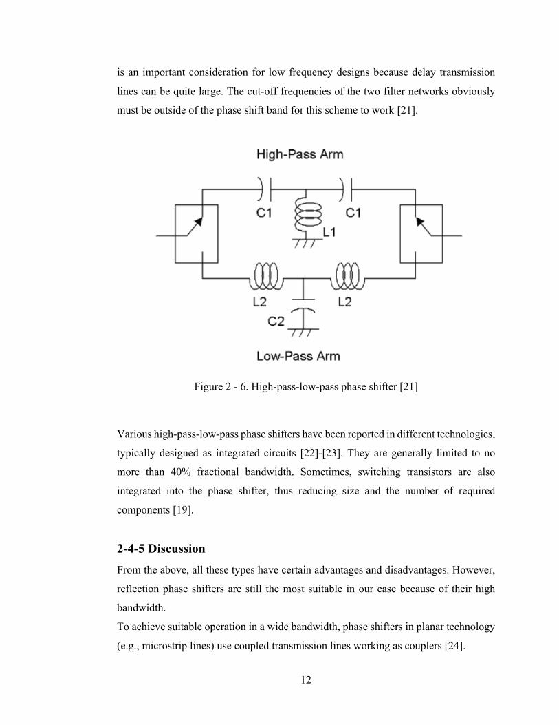
12
is an important consideration for low frequency designs because delay transmission
lines can be quite large. The cut-off frequencies of the two filter networks obviously
must be outside of the phase shift band for this scheme to work [21].
Figure 2 - 6. High-pass-low-pass phase shifter [21]
Various high-pass-low-pass phase shifters have been reported in different technologies,
typically designed as integrated circuits [22]-[23]. They are generally limited to no
more than 40% fractional bandwidth. Sometimes, switching transistors are also
integrated into the phase shifter, thus reducing size and the number of required
components [19].
2-4-5 Discussion From the above, all these types have certain advantages and disadvantages. However,
reflection phase shifters are still the most suitable in our case because of their high
bandwidth.
To achieve suitable operation in a wide bandwidth, phase shifters in planar technology
(e.g., microstrip lines) use coupled transmission lines working as couplers [24].

13
2-5 Planar Couplers
As mentioned, since we chose the reflection type, we need directional hybrid couplers.
A simple directional coupler is just two transmission lines put close together, such that
the secondary line can absorb energy from the field created around the primary. The
resulting structure can have many properties, some of which are desirable and others
are not. Coupled line couplers are not "DC connected", as opposed to "direct coupled"
couplers such as the Wilkinson and the branch-line. Coupled lines occur when two
transmission lines are close enough in proximity so that energy from one line passes to
the other. The Through Line, or Main Line, needs to be designed for the best possible
match and must be capable of handling whatever the maximum input power level is
specified to be. The quality of match for the Coupled Line will affect the directivity of
the coupler. Directivity is a measure of “how well the coupler isolates two opposite-
travelling (forward and reverse) signals” [25].
However, some types of couplers will show a greater sensitivity to this than others. For
example, if by using both ends of a single coupled line to provide Forward and Reverse
coupled output, then the match of this line and also the match of the external
components is absolutely critical to directivity. However, if the coupled line will have
a termination at one end, then this may be tuned to optimize directivity. It is perfectly
feasible to create a dual directional coupler using two separate coupled lines each of
which is terminated at one end.
Usually we are talking about lines that are coupled over a quarter-wave section, or
multiple sections. Bandwidth is greater than in interconnected transmission line
(uncoupled line) circuits like the branch-line coupler. Lines can be coupled in at least
two ways.
Hybrid couplers are the special case of a four-port directional coupler that is designed
for a 3-dB (equal) power split. Hybrids come in two types, 90 degree or quadrature
hybrids, and 180 degree hybrids. Hybrid couplers are often used in creating reflection
phase shifters.
14
2-5-1 Edge coupling configuration
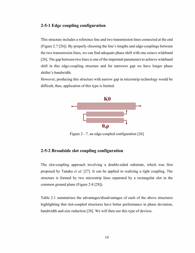
This structure includes a reference line and two transmission lines connected at the end
(Figure 2.7 [26]). By properly choosing the line’s lengths and edge-couplings between
the two transmission lines, we can find adequate phase shift with one octave wideband
[26]. The gap between two lines is one of the important parameters to achieve wideband
shift in this edge-coupling structure and for narrower gap we have longer phase
shifter’s bandwidth.
However, producing this structure with narrow gap in microstrip technology would be
difficult, thus, application of this type is limited.
Figure 2 - 7. an edge-coupled configuration [26]
2-5-2 Broadside slot coupling configuration
The slot-coupling approach involving a double-sided substrate, which was first
proposed by Tanaka et al. [27]. It can be applied to realizing a tight coupling. The
structure is formed by two microstrip lines separated by a rectangular slot in the
common ground plane (Figure 2-8 [28]).
Table 2.1 summarizes the advantages/disadvantages of each of the above structures
highlighting that slot-coupled structures have better performance in phase deviation,
bandwidth and size reduction [28]. We will then use this type of devices.

15
Figure 2 - 8. Slot coupling configuration [28]
Table 2 - 1 comparison between slot-coupled and edge-coupled configurations [29]
Edge-coupled Slot-coupled
Operating bandwidth High Very high
Characteristics
Return loss High High
Insertion loss Low Relatively low
Phase ripple Normal Very low
Design issues very narrow gap between transmission lines
Complexity due to double layers circuit
2-6 Phase Shifter Designs
The first published wideband phase shifter based on a Slot-coupled structure was the
Schiffman phase shifter [26]. After that, several structures have been proposed [30]-
[35]. For instance, in [31], different structures based on Schiffman structure have been

16
discussed. In addition to common Schiffman’s structures, others configurations such
as SIW [36] and loaded transmission line phase shifters [37] have be proposed.
Slot coupled transmission signal’s structures consist generally on two sub layers. For
analyzing these structures, odd and even mode analysis are used. This part will be
covered in the next chapter.
2-6-1 Schifman’s phase shifter
As mentioned earlier, the Schiffman’s phase shifter has been the first published
wideband phase shifter design with 90o’ difference phase [38]. This differential phase
shifter consisted of two transmission lines, a reference transmission line and an edge
coupling due to two beside lines. By properly choosing the lines length and coupling
rate, the phase difference in the whole bandwidth can be maintained relatively constant,
i.e., 90o. Notice that Schiffman’s work was on strip line structure, which scattered odd
and even modes in the coupled line have identical phase speed. Therefore, when this
type is designed with microstrip lines, unequal speed of odd and even modes will lead
to weak phase shifter operation.
In [38], two identical parallel-coupled lines were connected at their end and the
frequency behavior of the rippled lines network has been evaluated and the image
impedance equations and constant phase defined as
(2-1)
and
(2-2)
Zr ϕ
ZI = Z0oZ0e
cos(ϕ ) =
Z0eZ0o
− tan2θ
Z0eZ0o
+ tan2θ

17
where Z0e is the characteristic impedance in even-mode (when equal in-phase currents
flow in both lines) and Z0o represents the characteristic impedance in odd-mode (when
equal out-of-phase currents flow in both lines). Also ) = %3 is the electrical length of
a uniform line of length - and phase constant %.
The most elementary form of such a network is termed Type-A network. The
Schiffman’s method for reducing the maximum phase error of type-A was to connect
another differential phase shifter network to the system, which has symmetric to
neutralize each other’s. This structure, called error-correcting network, consists of two
separate structures (Figure 2-9 [38]), a transmission line with the length of 2ml and a
coupled-line’s part with the length of 2ml, with 4 = ./'/./6.
According to the parameters 4 and , we can minimize the bandwidth’s error [38].
Therefore a type-B structure was designed to reduce the error by taking m = 3,
and , leading to a maximum 0.7o phase error in about one octave bandwidth
(Figure 2-10 [38]). In practice, the structure can be simplified by removing equal
lengths of uniform transmission line from each branch, without affecting differential-
phase response. Such a reduction is illustrated in figure for the Type-B network.
2-6-2 Mosko-Shelton’s constant phase shifter and directional coupler
To gain more bandwidth with an acceptable phase ripple by using the edge-coupling
method, Mosko and Shelton have proposed an approximate method for making
constant phase shifting, which includes different parts of a quarter of parallel coupled
wavelength [39]. The main problem with this method, which is generally for edge-
coupling phase shifters, is the need of high coupling for gaining large bandwidth.
Therefore, it may be impractical. Mosko and Shelton proposed to use series connection
to minimize this effect. Another problem of these structures is the large size of these
multi-part structures.
Δϕ
m
ρ1 = 4.1
ρ2 = 2.4

18
Figure 2 - 9. Error-correcting network and its two possible differential phase responses
[38].

19
Figure 2 - 10. Type-B network and its differential phase response.

20
Figure 2 - 11. Configuration of multi-section directional coupler. a) required coupling
response of multi-section coupler. b) decomposition of coupling response
2-6-3 Abbosh wideband phase shifter
In [40], Abbosh proposed a new approach in designing a phase shifter that exhibits
good properties in UWB (which is appropriate to our work). This method was used to
design 30 and 45o UWB phase shifters with size of 2.5cm x 2cm (Figure 2-12, [40]).
This structure is formed by two ellipsoid microstrip patch connected to input and output
microstrip lines. Upper and lower layers have been placed in front of each other. The
coupling between these patches takes place in the ellipsoid gap (ground level, middle
layer). Note that the ellipsoid form can provide a constant coupling coefficient in UWB.
Results showed a differential deviation and ripple less than 1 dB as well as a return
loss better than 10 dB. ±3!

21
Figure 2 - 12. Phase shifter a) upper layer b) middle layer c) lower layer d) whole
structure [40]
Figure 2 - 13 Phase shifter as a four-port device with two open-circuit ports [40]
The analysis starts by assuming the phase shifter as a four-port device. Like figure 2-
13 two ports are considered open circuit (with this assumption the reflection coefficient
at ports 3 and 4 will be 1). Considering that the designed phase shifter has coupling C
22
between upper and lower patches, the scattering parameters of the above structure
would be:
(2-3)
(2-4)
where βef represents the effective phase constant in the medium of the coupled
structure.
As mentioned before, edge coupling in single layers’ structures and the slot-coupled
method are two important procedures for band widening [39]. From that, enhanced
structures have been proposed [28]-[33]. For instance, in [40], an improved
Schiffman’s structure with modifying ground plane underneath coupled lines has been
proposed. This 1.5-3.1 GHz structure has phase ripple and 0.5 dB amplitude ripple.
In [31], Sorn has improved the Abbosh’s structure by adding a gap in slot-coupled
output and gained 90o phase difference. This structure works in 3-7 GHz bandwidth. A
0.75-2.4 GHz and 90o phase shifter with stepped impedance open stub and coupled line
with 1.1 dB amplitude ripple and phase deviation has been proposed in [34]. Also
in [35], a 90o phase shifter, with loaded transmission line and T form open stub, and
operating in the 2.3-5.5 GHz frequency range, has been presented. This structure has
phase deviation and less than 0.6 dB loss. In [36], 45o, 90o, and 135o phase shifters
with referenced line and coupled lines have been described. Working in the range of
2.24-3.55 GHz, they show phase ripple and loss less than 0.9 dB.
2-7 Conclusions
In this chapter, we analyzed different wideband differential phase shifters. We
reviewed the advantages and disadvantages of conventional methods for phase shifter’s
S11 =1−C 2 (1+ sin2(βef l))
1−C 2 cos(βef l)+ j sin(βef l)⎡⎣
⎤⎦2
S21 =j2C 1−C 2 sin(βef l)
1−C 2 cos(βef l)+ j sin(βef l)⎡⎣
⎤⎦2
5!
5!
6.4!
5!

23
design (Table 2-2). By comparing different structures, the operating frequency band of
slot-coupling structures is higher compared to other structures. The other benefit of this
structure is its smaller structure size and lower ripple. We, therefore, opted for a
wideband reflective phase shifter based on double layer slot-coupled coupler
configuration. From that, we first designed the required coupler as detailed in the next
chapter.
Table 2 - 2. Comparison between different topologies of phase shifters
type advantages disadvantages
Switched-line Perfect for true time delay Variable insertion loss
Reflection-type Better matching at each
port
Occupy more chip area
and more loss because of
coupler
Loaded-line The phase vs frequency is
more flatter
Impossible to have a
matched circuit in both
states
High-pass-low-pass Provide near constant
phase shift over an octave
or more
Limited to no more than
40% fractional bandwidth

24
Chapter Three
Coupler Design
In the previous chapter, we discussed about the different kinds of phase shifters and
retained the reflective phase shifter with slot-coupling configuration. To achieve our
design, we will start with the Abbosh’s structure, enhancing it to uniform the
coupling between transmissions lines on upper and lower sub layers at the minimum
and maximum frequencies of the UWB band (3.1-10.6 GHz). Then, we will vary the
sub layer dimensions to decrease the return loss and insertion loss. To do so, we have
to start by designing a wideband hybrid coupler with two loaded ports.
3-1 Design Approach
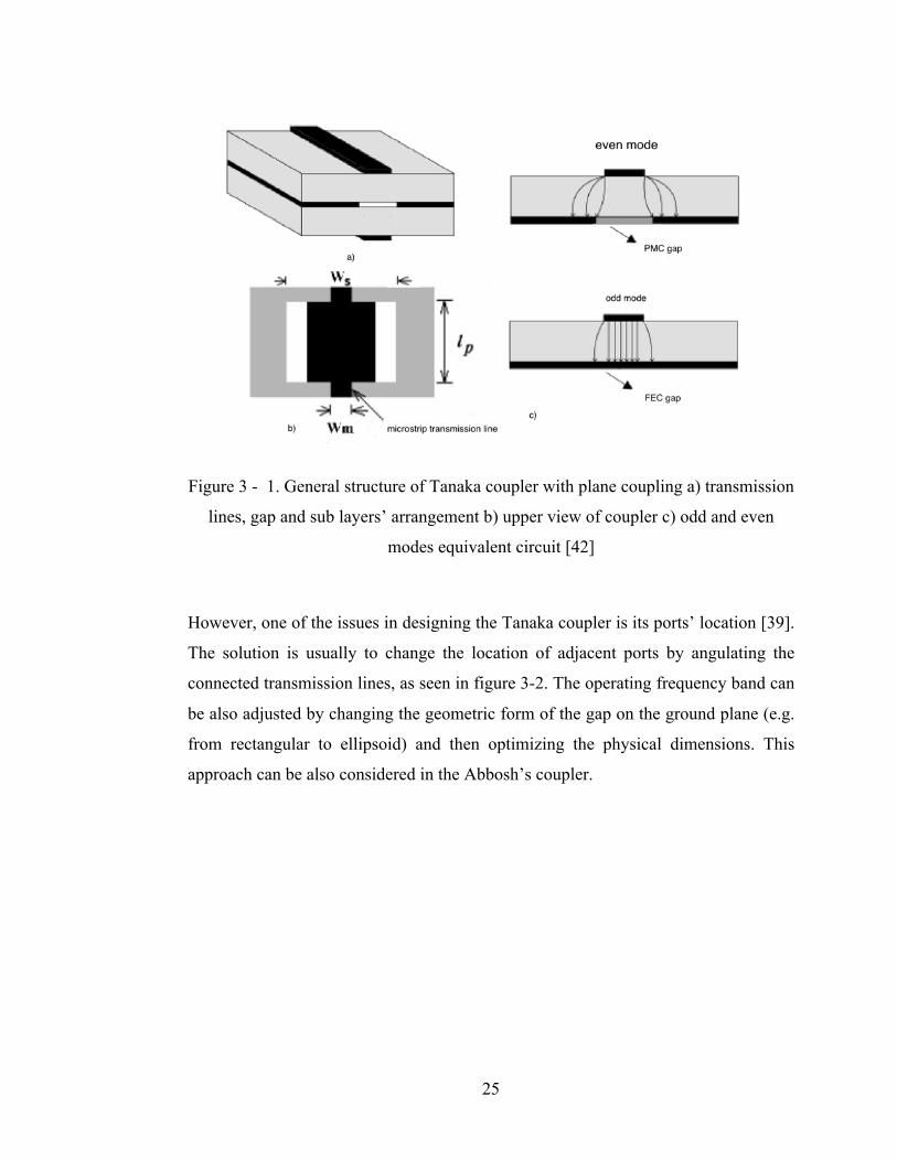
To design a coupler with tight coupling in a so wide frequency range, we retained the
plane coupling structure introduced by Tanaka (Figure 3-1, [41]). Its smaller size and
wideband operating frequency are the main reasons we selected it.
Its smaller size (e.g. compared to Schiffman’s structure) is due to the use of a plane
coupling between the two transmission lines that are placed on upper and lower sub
layers (via the gap on the ground plane). This plane coupling is substituted to the edge
coupling in the Schiffman’s structure. Also, its phase ripple in the operating band is
relatively less compared to other microstrip structures [39].
Figure 3-1-a shows the general form of this structure. Figure 3-1-b depicts the
rectangular Tanaka coupler structure. Figure 3-1-c shows the electric field lines for odd
and even modes excitation.
45!
25
Figure 3 - 1. General structure of Tanaka coupler with plane coupling a) transmission
lines, gap and sub layers’ arrangement b) upper view of coupler c) odd and even
modes equivalent circuit [42]
However, one of the issues in designing the Tanaka coupler is its ports’ location [39].
The solution is usually to change the location of adjacent ports by angulating the
connected transmission lines, as seen in figure 3-2. The operating frequency band can
be also adjusted by changing the geometric form of the gap on the ground plane (e.g.
from rectangular to ellipsoid) and then optimizing the physical dimensions. This
approach can be also considered in the Abbosh’s coupler.

26
Figure 3 - 2. Offered coupler structure’s layers with plane coupling
3-1-1 Odd and even mode analysis
We designed the hybrid coupler on Rogers RO4003C substrate with 20 mil thickness
with dielectric constant εr=3.38 mainly because of its availability.
The first step was to compute the odd and even impedances for a 3 dB coupling and
50Ω characteristic impedance Z0 using the following relations [42]
kc(dB) = 20 logZ0e − Z0oZ0e + Z0o
⎛⎝⎜
⎞⎠⎟
(3-1)
Z0 = Z0eZ0o (3-2)
27
leading to Z0e = 120.5Ω and Z0o = 20.7Ω . Then, it is necessary to analyze the coupler
operation in dual modes.
When the odd mode is excited, the gap on ground plane can be replaced by a perfect
electric conductor (PEC). The upper part of the resulting equivalent coupler converted
to a microstrip line with Z0o characteristic impedance. The related line width, wp , can
be then obtained using the standard designing equations for microstrip lines.
As for the even mode signal’s excitation, the perfect magnetic conductor (PMC) is
substituted to the gap on the ground. The magnetic plane will push the electric field
from the microstrip ports to the outside area of the parallel planes because the magnetic
conductor in the lower plane will not let the electric field to be perpendicular on its
surface. Therefore, the even mode signal moves outside the area of parallel planes as
shown in figure 3-1-c. To allow the even mode signal moving smoothly from the port
to the lines, it is recommended to modify the shape of the upper and lower transmission
lines as well as the ground gap from rectangular to ellipsoid (figure 3-2) [42].
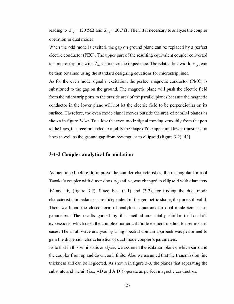
3-1-2 Coupler analytical formulation
As mentioned before, to improve the coupler characteristics, the rectangular form of
Tanaka’s coupler with dimensions wp and ws was changed to ellipsoid with diameters
W and Ws (figure 3-2). Since Eqs. (3-1) and (3-2), for finding the dual mode
characteristic impedances, are independent of the geometric shape, they are still valid.
Then, we found the closed form of analytical equations for dual mode semi static
parameters. The results gained by this method are totally similar to Tanaka’s
expressions, which used the complex numerical Finite element method for semi-static
cases. Then, full wave analysis by using spectral domain approach was performed to
gain the dispersion characteristics of dual mode coupler’s parameters.
Note that in this semi static analysis, we assumed the isolation planes, which surround
the coupler from up and down, as infinite. Also we assumed that the transmission line
thickness and can be neglected. As shown in figure 3-3, the planes that separating the
substrate and the air (i.e., AD and A’D’) operate as perfect magnetic conductors.
28
Figure 3 - 3. The coupler model for semi-static analysis [42]
So the existence of the gap in the mutual ground plane does not affect the coupler’s
odd mode characteristics.
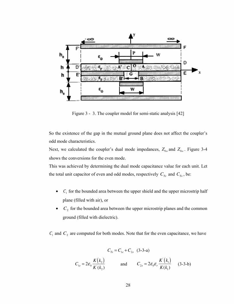
Next, we calculated the coupler’s dual mode impedances, Z0o and Z0o . Figure 3-4
shows the conversions for the even mode.
This was achieved by determining the dual mode capacitance value for each unit. Let
the total unit capacitor of even and odd modes, respectively CTe and CTo , be:
• C1 for the bounded area between the upper shield and the upper microstrip half
plane (filled with air), or
• C2 for the bounded area between the upper microstrip planes and the common
ground (filled with dielectric).
C1 and C2 are computed for both modes. Note that for the even capacitance, we have
CTe = C1e +C2e (3-3-a)
C1e = 2ε0K k2( )K ' (k2 )
and C2e = 2ε0ε rK ' k1( )K(k1)
(3-3-b)

29
where K(k) is the type one elliptical integral K '(k) = K(k ') as k ' = 1− k2 and
K(k)K '(k)
=
2πln 2 1+ k
1− k⎛⎝⎜
⎞⎠⎟
0.707 ≤ k ≤1
π
2 ln 1+ 1− k2
1− 1− k2⎛
⎝⎜⎜
⎞
⎠⎟⎟
0 ≤ k ≤ 0.707
⎧
⎨
⎪⎪⎪⎪
⎩
⎪⎪⎪⎪
(3-4)
Figure 3 - 4. Conversions to find unit capacitor of coupler’s even mode

30
k1 and k2 are determined from
k1 =sinh2 πws
4h⎛⎝⎜
⎞⎠⎟
sinh2 πws
4h⎛⎝⎜
⎞⎠⎟ + cosh
2 πws
4h⎛⎝⎜
⎞⎠⎟
and k2 = tanhπwp
4h⎛⎝⎜
⎞⎠⎟
(3-5)
Then, going back to the original design of Tanaka (figure 3-1), it is possible to deduce
the length lp and width wp of the middle transmission line, as well as the length ls
and width ws of the gap.
Finally, the effective dielectric constant εeffe( ) and the characteristic impedance (Zoe )
for the even mode can be obtained by
εeffe =CTe
CTe(ε r →1)= ε r
K '(k1)K(k1)
+ K(k2 )K '(k2 )
⎡
⎣⎢
⎤
⎦⎥ /
K '(k1)K k1( ) +
K(k2 )K '(k2 )
⎡
⎣⎢
⎤
⎦⎥ (3-6)
Zoe =60πεeffe
K '(k1)K(k1)
+ K(k2 )K '(k2 )
⎡
⎣⎢
⎤
⎦⎥
−1
(3-7)
Note that, similarly, the BB’ plane in figure 3-3 works as a perfect magnetic conductor,
leading to the total capacitor in the odd mode as:
CTo = C1o +C2o (3-8)
C1o = 2ε0K k4( )K ' k4( ) and C2o = 2ε0ε r
K ' k3( )K k3( ) (3-9)
with
k3 = tanhπwp
4h⎛⎝⎜
⎞⎠⎟
and k4 = tanhπwp
4ho
⎛⎝⎜
⎞⎠⎟
(3-10)
31
The effective dielectric constant εeffe( ) and the characteristic impedance (Zoe ) of the
odd mode can be then deduced as
εeffe =CTo
CTo(ε r →1)= ε r
K '(k3)K(k3)
+ K(k4 )K '(k4 )
⎡
⎣⎢
⎤
⎦⎥ /
K '(k3)K k3( ) +
K(k4 )K '(k4 )
⎡
⎣⎢
⎤
⎦⎥ (3-11)
Zoo =60πεeffo
K '(k3)K(k3)
+ K(k4 )K '(k4 )
⎡
⎣⎢
⎤
⎦⎥
−1
(3-12)
The next step was to determine the coupler’s characteristics using MATLAB. The Zoo
and Zoe are linked with the values of ws ,wp , and the substrate thickness. So, with a
coupling kc( ) of 3 dB and a line characteristic impedance Z0( ) of 50Ω , Zoo and Zoe
can be achieved by equation (3-1).
Now we have two unknown variablesws and wp and two equations. The system was
solved after 50 iterations using the newton method in MATLAB. The final results give
78 = 6.5<< and 7= = 4.2<<. Once the transverse dimensions obtained, we had to
compute the longitudinal dimensions.
Now we use an approach, which consists to start from the design method described by
Schiffman, i.e., to use the concept of two coupled quarter-wavelength transmission
lines. Note that the geometric shapes of the transmission lines and the gap on the ground
plane were not taken into account during simulations. In fact, the above equations were
general and independent of the shapes. We therefore included such information by
starting the simulations with the initial design of Tanaka shown in figure 3-1.
Then, by considering the operating frequency range, 1.2-6.0 GHz, the central frequency
will be 3.6 GHz. For the design, we selected the cost-effective Rogers’ substrate
RO4003C with a relative permittivity &A = 3.38 and 20 mil thickness (equals to 0.508
mm). The quarter-wavelength length of the transmission line will be:
-= = -8 =D
E FG= H
E( FG= 11.33<< (3-13)

32
However, the above results are for a rectangular coupler shape. Thus, after determining
the equations for the rectangular coupler, we can use the equivalence principle to find
the equations for an elliptical coupler, assuming that the length of the rectangular
coupler is equal to the elliptical coupler.
Let L and LS be the respective lengths of the patch and the gap, and W and Ws the
corresponding widths (figure 2-2). With the above assumption, converting the gained
dimensions from rectangular to ellipsoid can be achieved as: (geometric equivalence)
L = lp + lp2 +wp
2( ) / 2 LS = ls + ls
2 +ws2( ) / 2 (3-14)
J ≈ 1.273(7=×-=)/P J8 ≈ 1.273(78×-8)/P8 (3-15)
3-2 Designing the hybrid coupler
The above equations can be used to design a hybrid coupler for different frequencies.
As for the operating bandwidth, it is determined based on the application specifications.
In this thesis, the purpose is to design a hybrid coupler with suitable characteristics in
the 1.2-6 GHz operating bandwidth with minimum return loss, phase and magnitude
ripple.
Designed at a central frequency of 3.6 GHz, the optimized dimensions of the designed
coupler (Figure 3-5) are summarized in Table 3-1.
The simulated coupler’s characteristics, shown in figure 3-6, are a return loss greater
than 23 dB in the whole 1.2-6 GHz frequency bandwidth with 137% frequency
bandwidth (BW = Δf / f 0) relatively to the central frequency, as well as a magnitude
and phase unbalanced less than 0.75! and 0.4 dB, respectively. This design has been
also successfully compared to existing designs as summarized in Table 3-2.

33
Figure 3 - 5. the offered wideband structure layers in 1.2-6 GHz frequency band with
plane coupling
Table 3 - 1 Dimensions of the designed coupler in 1.2-6 GHz frequency band.
Parameters (mm)
Wm50 Ws1 W1 Ws W Ls1 L1 LS L
1.1 1.05 1.4 11 7 4.5 5.2 10.8 11

34
(a)
(b)
(c)

35
(d)
Figure 3 - 6.Simulation results of the hybrid coupler in 1.2-6 GHz frequency band
a) reflective coefficients b) transmission coefficients c) phase shift d) phase and
amplitude unbalance.
3-3 Manufactured coupler
in this section we compared the results of manufactured coupler with the simulated
ones (Figure 3-7). In the simulation the wave ports are used and the connectors are not
included. Also we didn’t simulate the holes and screws on the board. We used the
Vector Network Analyzer with matched load as our test equipment.
Figure 3 - 7. The manufactured coupler measurement results.

36
Table 3 - 2 Comparison of the designed coupler characteristics vs. existing published
works.
Couplers’ characteristics
Structure
Ref. Fractional
Bandwidth
(%)
Frequency
band
(GHz)
Transmission
coefficient
(dB)
Phase
ripple
( ! )
137 1.2-6 3± 0.4dB ±0.75!
Elliptical shaped slot-
coupled microstrip coupler
our
work
42 3.6-5.5
3± 0.5dB ±1! N-section microstrip
tandem structure coupler [43]
180 1-9
3± 0.65dB
±5!
Vertically installed planar
multi section quadrature
hybrid coupler
[44]
111 0.8-2.8
1dB
±1.5!
Rat-race couplers with
coupled-line section and
impedance transformers
[45]
109 3.1-10.6
3±1dB
6 ±1.4dB
10 ±1.5dB
±1!
Elliptical shaped slot-
coupled microstrip coupler [46]
120 2-8
3±1.5dB
±7!
CPW slot-coupled
directional coupler [47]
109 3.1-10.6
3± 0.75dB
±2!
Rectangular shaped slot-
coupled microstrip coupler [48]
161 1.2-12
10 ± 0.6dB
±0.7!
Multi section corrugated
slot-coupled directional
coupler
[49]

37
Note that, to the best of the authors’ knowledge, there is no microstrip phase shifter in
this frequency range with this large bandwidth (137%). Furthermore, the designed
phase shifter’s characteristics are better than those mentioned articles.
3-3 Conclusion
In this chapter, we discussed about the hybrid coupler design approach and analytical
formulation. The simulations are performed in HFSS and ADS. The simulated coupler
exhibits a return loss greater than 23 dB in the whole desired 1.2-6 GHz frequency
bandwidth (137%) as well as a magnitude and phase unbalanced less than 0.75! and 1
dB, respectively for the measured results.

38
Chapter Four
Differential Phase Shifter Design
As already mentioned, the purpose of this thesis is to design a wideband differential
phase shifter operating in the 1.2-6 GHz frequency band. For this purpose, we used the
concept of reflective phase shifters.
For building a reflective phase shifter, we used the wideband hybrid coupler we
designed in previous chapter, while focusing on the load. In a first step, we designed
the required reactance load as a lumped inductor or capacitor.
After obtaining its value, the load was connected between the two output ports of the
designed coupler while the two other ports were used as input and output of the phase
shifter. Thus, the desired differential phase can be obtained by comparison with a
reference line.
In a second step, we modeled the lumped load as an equivalent microstrip line in order
to obtain a planar structure.
4-1 Designing the differential reflective phase shifter
4-1-1 Theoretical approach
As stated, the purpose was to obtain a reflective differential phase shifter. To start, the
analytic expression of the load should be found. Let port 1 and port 2 of the designed
4-ports dual mode coupler be the respective input and output port of the phase shifter

39
(Figure 4-1). In order to create a certain coupling kc between the upper and lower
patches, the corresponding reflective waves b1 and b2 can be computed as:
b1 =jkc sinθa3 + 1− kc
2a41− kc
2 cosθ + j sinθ
b2 =jkc sinθa4 + 1− kc
2a31− kc
2 cosθ + j sinθ (4-1)
with θ the electrical length of the coupled structure, which can be related to the
physical length l and the effective physical constant βef by:
θ = βef l (4-2)
leading to
βef =
βe + βo
2= 360!
ε rλ
(4-3)
In the above equation, βe and βo are the dual mode constants, λ is the free space
wavelength and ε r the substrate dielectric constant.
By assuming that port 2 (output port) is matched, the reflective signal in ports 3 and 4
will be as follows:
b3 =jkc sinθa1
1− kc2 cosθ + j sinθ
b4 =1− kc
2a11− kc
2 cosθ + j sinθ (4-4)
40
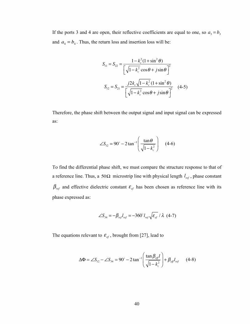
If the ports 3 and 4 are open, their reflective coefficients are equal to one, so a3 = b3
and a4 = b4 . Thus, the return loss and insertion loss will be:
S11 = S22 =1− kc
2 (1+ sin2θ )
1− kc2 cosθ + j sinθ⎡
⎣⎤⎦2
S12 = S21 =j2kc 1− kc
2 (1+ sin2θ )
1− kc2 cosθ + j sinθ⎡
⎣⎤⎦2 (4-5)
Therefore, the phase shift between the output signal and input signal can be expressed
as:
∠S12 = 90! − 2 tan−1 tanθ
1− kc2
⎛
⎝⎜
⎞
⎠⎟ (4-6)
To find the differential phase shift, we must compare the structure response to that of
a reference line. Thus, a 50Ω microstrip line with physical length lref , phase constant
βref and effective dielectric constant εef has been chosen as reference line with its
phase expressed as:
∠S34 = −βref lref = −360!lref εef / λ (4-7)
The equations relevant to εef , brought from [27], lead to
ΔΦ = ∠S12 −∠S34 = 90! − 2 tan−1 tanβeff l
1− kc2
⎛
⎝⎜
⎞
⎠⎟ + βeff lref (4-8)

41
4-1-2 Differential reflective phase shifter’s formulation
Following the above equations, we loaded the coupler’s ports to determine the phase
shift coming from it. Let Γ be the reflection coefficient. The new scattering matrix
parameters S’ (S matrix with loads), will be as follows:
S11' = S22
' = Γ 1− kc2 (1+ sin2θ )
1− kc2 cosθ + j sinθ⎡
⎣⎤⎦2
S12' = S21' = Γ
j2kc 1− kc2 (1+ sin2θ )
1− kc2 cosθ + j sinθ⎡
⎣⎤⎦2 (4-10)
The phase of S12' can be computed by summing the load phase and the phase of S12 .
∠ ′S12 = ∠S12 +∠Γ = 90! − 2 tan−1 tanθ1− kc
2
⎛
⎝⎜
⎞
⎠⎟ +∠Γ (4-11)
Then we needed to compare the phase with a reference line with suitable length lref as
its phase is given (equation (3-32)) as
∠ ′S12 = ∠S12 +∠ ′S34 = −βref lref (4-12)
and the final phase shift of reflective phase shifter will be as follows:
∠ ′Φ = ∠ ′S12 −∠ ′S34 = 90! − 2 tan−1 tanβeff l
1− kc2
⎛
⎝⎜
⎞
⎠⎟ +∠Γ + βref lref (4-13)

42
Figure 4 - 1 Schematic version of offered reflective phase shifter by using the loaded
symmetric directional coupler
As can be seen, we can design different phase shifters only by changing the load.
Although loading has most effects on changing the phase, the load also has an impact
on the magnitude or phase of other scattering parameters (according to (4-10)). In this
case, we had to change the dimensions of the coupler, as it will be discussed later.
4-2 Design Results with Elliptical-Shaped Microstrip Load
Following the coupler’s design process and formulation described in parts 3-3 and 3-
2-2, respectively, its geometrical dimensions were obtained (Figure 4-2 and Table 4-
1). As mentioned, the circuit has been designed on a Rogers RO4003C two-layer board
with 20 mil thickness, dielectric permittivity ε r = 3.38 and central frequency 3.6 GHz.
Table 4- 1 Designed coupler dimensions for reflective phase shifter
Parameters (mm) Coupler’s
characteristics Wm50 W1 W1 Ws W Ls1 L1 LS L
1.1 1.05 1.4 11 7 4.5 5.2 10.8 11 Values
43
Figure 4 - 2 a) General structure of the reflective phase shifter with elliptical load, b)
the upper and c) lower transmission lines with elliptical shaped patch and load
Also, by computing the load’s reflective coefficient value we can achieve the required
phase shift. So, we first determined the Γ value for the desired phase shift in order to
get the initial dimensions of the elliptical load using ADS. Then, we optimized its
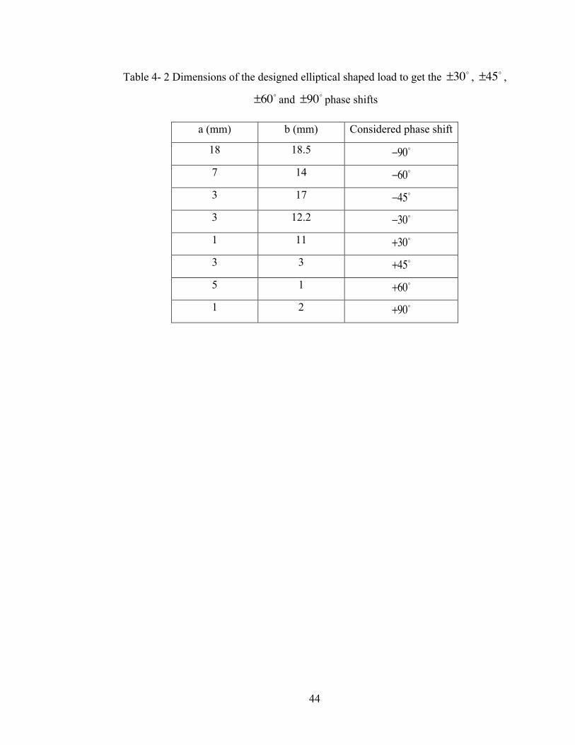
dimensions in HFSS (Table 4-2). As mentioned, the structure should be capable of
creating the −90! to +90! phase shift on the 1.2-6 GHz frequency band as well as
different other phase shifts by changing the dimensions of the elliptical shaped load in
coupler’s ports. Therefore, the designed load dimensions for ±30! , ±45! , ±60! and
±90! phase shifters have been also brought in Table 4-2.
As can be seen in figure 4-3, the reflection and crossing coefficients of the designed
structures are less than 10 dB and 1 dB, respectively. The −90! , −60! , −45! , −30! , 30!
, 45! , 60! and 90! phase shifters exhibit a respective 1.6! , 1.2! , 1! , 1.2! , 1.1! ,
2.1! , 1.25! and 2! phase deviation in the operating bandwidth. Therefore, the proposed
phase shifters have a phase ripple less than 2.1! in a 137% frequency bandwidth
(BW = Δf / f 0) relatively to the central frequency.
44
Table 4- 2 Dimensions of the designed elliptical shaped load to get the ±30! , ±45! ,
±60! and ±90! phase shifts
a (mm) b (mm) Considered phase shift
18 18.5 −90! 7 14 −60! 3 17 −45! 3 12.2 −30! 1 11 +30! 3 3 +45! 5 1 +60! 1 2 +90!

45
(a)
(b)
(c)

46
(d)
Figure 4 - 3 a) phase shift, b) phase ripple, c) return loss, d) insertion loss of the
±30! , ±45! , ±60! and ±90! differential phase shifters with elliptical shaped
microstrip load in 1.2-6 GHz frequency band.
4-3 Parametric Analysis
In this part, our purpose is to analyze the effects on coupler’s characteristics caused by
changing the phase shifter parameters. Let us take the 45o phase shifter as illustration.
Figures 4-4 show the effect of changing a) the load’s dimensions on the phase shift, b)
the effect of changing the length of the reference line on the phase shift, c) the effect
of changing the load’s dimensions on the return loss, and d) the effect of changing the
load’s dimensions on the insertion loss. For all the simulations, the wave ports are used
and connectors not included.

47
(a)
(b)
(c)

48
(d)
Figure 4 - 4 Simulation results of the 45o differential reflective phase shifter for
parametric analysis a) the effect of changing the load’s dimensions on phase shift b)
the effect of changing the length of the reference line on the phase shift c) the effect
of changing the load’s dimensions on the return loss d) the effect of changing the
load’s dimensions on the insertion loss
From these figures, we can note that changing the length and the width of the elliptical
load, i.e., the load’s reactance, have a significantly impact on the phase shift but much
less effect on the return and insertion loss. So, we can control the phase shift by
changing the load in the ports. On the other hand, the length of the transmission line
has an important role in adjusting the required differential phase shift and choosing the
suitable length for the transmission line that would give the desired phase shift for the
considered load.
4-4 Manufacture and Test Results of the 45o Differential Phase Shifter
To demonstrate our design, we manufactured the 45o phase shifter using the parameter
values got from simulations (figure 4-5). The dimensions of the designed circuit with
the length of the reference line is 24<<×63<< which is equal 0.14*'((×0.3*'((
based on effective wavelength. The test results of the fabricated phase shifter are shown

49
in figure 4-6. From this figure, we can conclude that there is a little difference between
measured and simulated results. The return loss and insertion loss are better than 10 dB
and 1.5 dB, respectively, and the maximum phase ripple is 3°. For the measurement,
we used the Keysight (Agilent/HP) 8720ES Vector Network Analyzer as in figure 4-5.
The simulation is carried out considering the holes in where screws are located. We
had done simulation by considering the screws as some rod metals. And we have used
the wave ports and connectors are not included. It also might be a mismatch between
load and connectors. The simulations are performed in HFSS and ADS. The screws
can cause resonances. It also might be a mismatch between load and connectors.
a)

50
b)
Figure 4 - 5 a) Measurement system, b) the manufactured 45o phase shifter (top,
bottom and middle views).
Figure 4 - 6 Measurement results of the 45o phase shifter, Return and insertion loss

51
Figure 4 - 7 Comparing measurement and simulation results for S11
Figure 4 - 8. Comparing measured and simulated phase shift
4-5 comparison of the designed phase shifter with others
Because of its better response in terms of bandwidth, the elliptical load was used and
its dimensions varied to improve the phase shifter characteristics. Therefore, different
1.2-6 GHz phase shifters were designed with ±30! , ±45! , ±60! and ±90!
differential phase. The simulation and computation results show a maximum of 3! phase deviation in the 1.2-6 GHz frequency operating range. The return and insertion
loss are less than 10 dB and 1 dB, respectively. Such results can be successfully
compared to existing designs (Table 4-3), thus demonstrating the contributions made
in this area.
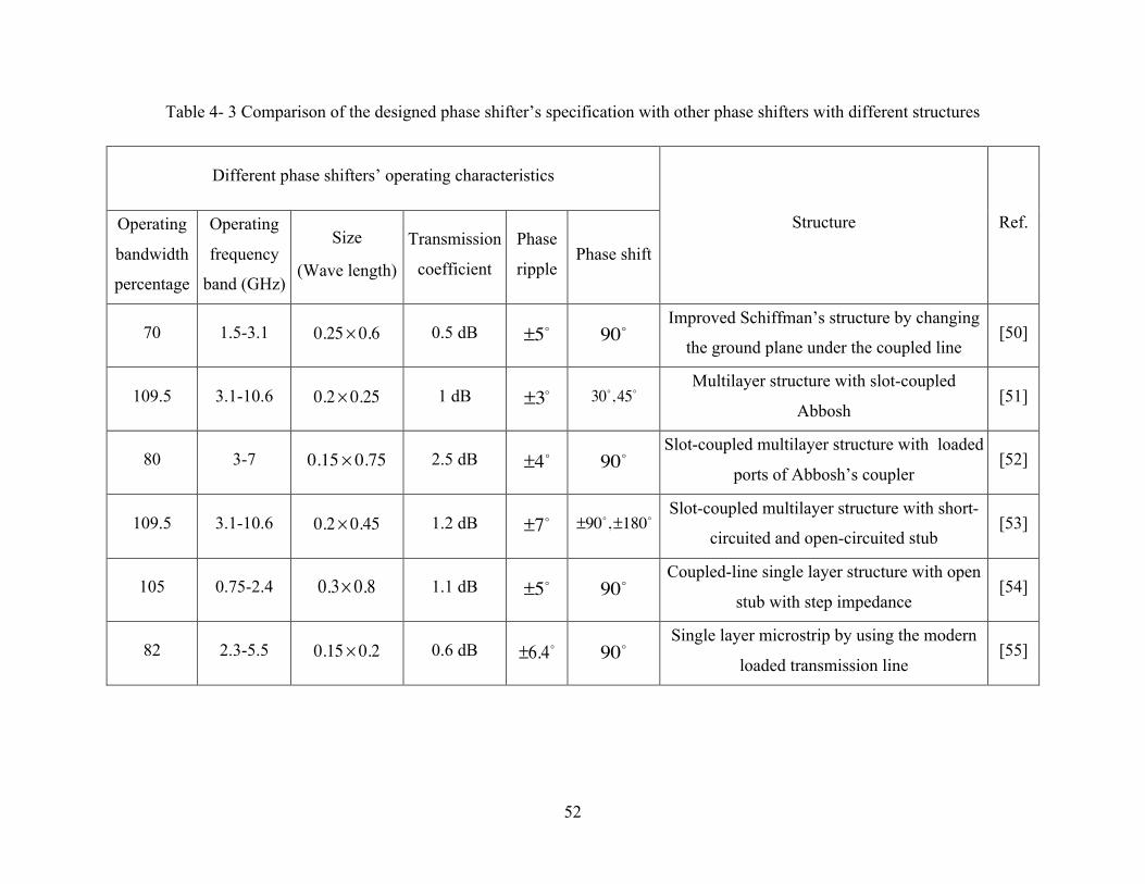
52
Table 4- 3 Comparison of the designed phase shifter’s specification with other phase shifters with different structures
Different phase shifters’ operating characteristics
Structure Ref. Operating
bandwidth
percentage
Operating
frequency
band (GHz)
Size
(Wave length)
Transmission
coefficient
Phase
ripple Phase shift
70 1.5-3.1 0.25 × 0.6 0.5 dB ±5! 90! Improved Schiffman’s structure by changing
the ground plane under the coupled line [50]
109.5 3.1-10.6 0.2 × 0.25 1 dB ±3! 30!, 45!
Multilayer structure with slot-coupled
Abbosh [51]
80 3-7 0.15 × 0.75 2.5 dB ±4! 90! Slot-coupled multilayer structure with loaded
ports of Abbosh’s coupler [52]
109.5 3.1-10.6 0.2 × 0.45 1.2 dB ±7! ±90!,±180!
Slot-coupled multilayer structure with short-
circuited and open-circuited stub [53]
105 0.75-2.4 0.3× 0.8 1.1 dB ±5! 90! Coupled-line single layer structure with open
stub with step impedance [54]
82 2.3-5.5 0.15 × 0.2 0.6 dB ±6.4! 90! Single layer microstrip by using the modern
loaded transmission line [55]
53
Different phase shifters’ operating characteristics
Structure Ref. Operating
bandwidth
percentage
Operating
frequency
band (GHz)
Size
(Wave length)
Transmission
coefficient
Phase
ripple Phase shift
105 3.1-10.6 0.5 × 0.8 1 dB ±9! 90! Single layer microstrip structure by using the
transmission line and electromagnetic model [56]
45 2.24-3.55 0.1× 0.5 0.9 dB ±5! 45
!,90!
135!
Multi-path single layer microstrip structure
with monolithic transmission line by using
the coupled line structure
[57]
137 1.2-6
0.2 × 0.43
(with
reference line)
1 dB ±2.1! ±30
!,±45!
±60!,±90!
Slot-coupled multilayer structure with
placing the elliptical-shaped load on
coupler’s port (we haven’t done process
variation)
our
work

54
4-6 Conclusion
In this chapter we designed reflective phase shifters in 1.2-6 GHz band. The
simulations are performed in HFSS and ADS. After the theoretical approach,
formulation and simulations, we compared the results with previous works. Also we
compared the measured and simulated results of the 45° differential phase shifter. The
simulation and computation results show a maximum of 3! phase deviation in the
operating frequency range. The return and insertion loss are less than 10 dB and 1 dB,
respectively.
55
Chapter 5
Conclusions and future works
5.1 Conclusions
In this thesis, we discussed about the design process of slot-couple wideband reflective
phase shifters. First, we detailed the concepts behind couplers and phase shifters. Then,
for each of them, we presented the related formulation to theoretically approximating
their geometrical dimensions in terms of the considered design parameters such as
coupling coefficient and required phase shift.
For band widening the phase shifter, the reflective phase shifter has been retained.
Therefore, a wideband coupler has been designed first using a modified Abbosh’s
structure. Such modification includes variation in the gap created on ground. This
change uniforms the coupling between transmissions lines on upper and lower sub
layers at, respectively, the minimum and maximum frequencies of the operating band.
To design the reflective phase shifter, we used the above coupler as its two ports are
loaded. Loading in ports has been achieved by placing a required reactance load (as
either lumped element or planar microstrip line).
The microstrip load first was simulated as an open circuit stub. Then we placed an
elliptical load, which was the best form in terms of operating bandwidth. All
simulations were performed in the full-wave HFSS software beside ADS. Our purpose
was to design a coupler with suitable characteristics such as providing the 3 dB
coupling in targeted 1.2 – 6 GHz frequency band with minimum return loss, phase and
amplitude imbalance while maximizing the operating bandwidth. This frequency
interval includes important frequency bands such as such as GPS, DCS, PCS, UMTS,
WiBro, Bluetooth, S-DMB, WiMax and WLAN. These frequencies have application

56
in satellite telecommunication, marine communication and mobile communication and
etc.
Once measured, the performance of the designed device was compared to recent works,
and, to the best of the author’s knowledge, there is no microstrip phase shifter in this
frequency range with the obtained bandwidth (137%). Furthermore, the designed phase
shifter’s characteristics are better than those mentioned in existing publications.
Furthermore, the designed phase shifter with elliptical load is capable of creating a
−90! to +90! phase shift on 1.2-6 GHz frequency range. Also, by changing the elliptical
shaped load dimensions, different phase shifts can be obtained.
Therefore, design and simulation of ±30! , ±45! , ±60! and ±90! differential phase
shifters were presented. The simulation and computation results show a maximum of
3° phase deviation, as well as return and insertion loss less than 10 dB and 1 dB
respectively.
5.2 Future works
As future direction to enhance this work, we can first use the stripline technology
instead of microstrip, since it has lower loss.
Also depending on the application needed, we can change our priorities. Here our main
priority was bandwidth.
Another option is changing the geometrical shapes of patch and slot based on
simulation’s feedbacks.
57
References
[1] Vijay K. Varadan, K. J. Vinoy, K. A. Jose, RF MEMS and their applications,
(Wiley, 2002) [2] Ian Robertson and Jim Turner, “MMIC Design”, Institution of Electrical
Engineers, Micheal Faraday House, London, 1995.
[3] Sunil Kansal, “4-Bit MMIC Digital Phase Shifter”, B.Eng thesis, Department of
Electrical Engineering, National University of Singapore, 1998/1999.
[4] A. M. Abbosh, "Ultra-Wideband Phase Shifters," in IEEE Transactions on
Microwave Theory and Techniques, vol. 55, no. 9, pp. 1935-1941, Sept. 2007.
[5] B. M. Schiffman, "A New Class of Broad-Band Microwave 90-Degree Phase
Shifters," in IRE Transactions on Microwave Theory and Techniques, vol. 6, no.
2, pp. 232-237, April 1958.
[6] J. P. Shelton and J. A. Mosko, "Synthesis and Design of Wide-Band Equal-
Ripple TEM Directional Couplers and Fixed Phase Shifters," in IEEE
Transactions on Microwave Theory and Techniques, vol. 14, no. 10, pp. 462-
473, Oct 1966.
[7] J. L. R. Quirarte and J. P. Starski, "Novel Schiffman phase shifters," in IEEE
Transactions on Microwave Theory and Techniques, vol. 41, no. 1, pp. 9-14, Jan
1993.
[8] Yong-Xin Guo, Zhen-Yu Zhang and Ling Chuen Ong, "Improved wide-band
Schiffman phase shifter," in IEEE Transactions on Microwave Theory and
Techniques, vol. 54, no. 3, pp. 1196-1200, March 2006.
[9] M. Sorn, R. Lech and J. Mazur, "Simulation and Experiment of a Compact
Wideband 90 Differential Phase Shifter," in IEEE Transactions on Microwave
Theory and Techniques, vol. 60, no. 3, pp. 494-501, March 2012.
[10] L. Guo and A. Abbosh, "Phase Shifters with Wide Range of Phase and Ultra-
Wideband Performance Using Stub-Loaded Coupled Structure," in IEEE
[11] A. Lüker, "Ferroelectric Phase Shifters," 2006. [Online]. Available:
http://microwaves101.com. Accessed: Aug. 15, 2016.
58
[12] E. Erkek, "S-Band Hybrid 4 Bit Phase Shifter Using Cots Components," MSC
Thesis, METU, Ankara, Turkey, 2009.
[13] Sunil Kansal, “4-Bit MMIC Digital Phase Shifter”, B.Eng thesis, Department of
Electrical Engineering, National University of Singapore, 1998/1999.
[14] S. K. Koul and B. Bhat, Microwave and Millimeter Wave Phase Shifters: Vol. I
Dielectric and Ferrite Phase Shifters, (Boston: Artech House, 1991).
[15] Vijay K. Varadan, K. J. Vinoy, K. A. Jose, RF MEMS and their applications, (Wiley, 2002)
[16] "Phase Shifter Fundamentals," 2013. [Online]. Available: http://www.rfmw.com.
Accessed: Aug. 15, 2016.
[17] I. Sarkas, “Analysis and Design of W-band Phase Shifters,” MSC Thesis,
University of Toronto, Toronto, Canada, 2010.
[18] S.Sasikumar and B. S. Narayanan, “Analysis of reflective type phase shifter for
millimeter wave application,” Signal Processing, Communication, Computing
and Networking Technologies (ICSCCN), 2011 International Conference on,
Thuckafay, 2011, pp. 342-346.
[19] T. Neil Ross, "Gallium Nitride Phase Shifters," PHD Thesis, Carleton University,
Ottawa, ON, Canada, 2015.
[20] "Loaded-Line Phase Shifters,”. [Online]. Available: http://microwaves101.com.
Accessed: Aug. 15, 2016.
[21] "High-pass/Low-pass Phase Shifters,”. [Online]. Available:
http://microwaves101.com. Accessed: Aug. 15, 2016.
[22] R. V. Garver, “Broad-Band Diode Phase Shifters,” in IEEE Transactions on
Microwave Theory and Techniques, vol.20, no. 5, pp.314-323, May 1972.
[23] C. Moye, G. Sakamoto and M. Brand, “A compact broadband, six-bit MMIC
phasor with integrated digital drivers,” Microwave Symposium Digest, 1990,
IEEE MTT-S International, Dallas, TX, 1990, pp. 457-460 vol.1.
[24] A. M. Abbosh, "Ultra-Wideband Phase Shifters," in IEEE Transactions on
Microwave Theory and Techniques, vol. 55, no. 9, pp. 1935-1941, Sept. 2007.
[25] "Directional Couplers and Bridges,". [Online]. Available:
http://www.keysight.com/. Accessed: Aug. 15, 2016.

59
[26] B. M. Schiffman, "A New Class of Broad-Band Microwave 90-Degree Phase
Shifters," in IRE Transactions on Microwave Theory and Techniques, vol. 6, no.
2, pp. 232-237, April 1958.
[27] T. Tanaka, K. Tsunoda and M. Aikawa, "Slot-coupled directional couplers on a
both-sided substrate MIC and their applications, "in Electronics and
Communications, vol. 72, no. 3, Japan 1989.
[28] A. M. Abbosh and M. E. Bialkowski, "Design of Compact Directional Couplers
for UWB Applications," in IEEE Transactions on Microwave Theory and
Techniques, vol. 55, no. 2, pp. 189-194, Feb. 2007.
[29] A. M. Abbosh, "Ultra-Wideband Phase Shifters," in IEEE Transactions on
Microwave Theory and Techniques, vol. 55, no. 9, pp. 1935-1941, Sept. 2007.
[30] J. P. Shelton and J. A. Mosko, "Synthesis and Design of Wide-Band Equal-
Ripple TEM Directional Couplers and Fixed Phase Shifters," in IEEE
Transactions on Microwave Theory and Techniques, vol. 14, no. 10, pp. 462-
473, Oct 1966.
[31] J. L. R. Quirarte and J. P. Starski, "Novel Schiffman phase shifters," in IEEE
Transactions on Microwave Theory and Techniques, vol. 41, no. 1, pp. 9-14, Jan
1993.
[32] Yong-Xin Guo, Zhen-Yu Zhang and Ling Chuen Ong, "Improved wide-band
Schiffman phase shifter," in IEEE Transactions on Microwave Theory and
Techniques, vol. 54, no. 3, pp. 1196-1200, March 2006.
[33] M. Sorn, R. Lech and J. Mazur, "Simulation and Experiment of a Compact
Wideband 90 Differential Phase Shifter," in IEEE Transactions on Microwave
Theory and Techniques, vol. 60, no. 3, pp. 494-501, March 2012.
[34] L. Guo and A. Abbosh, "Phase Shifters with Wide Range of Phase and Ultra-
Wideband Performance Using Stub-Loaded Coupled Structure," in IEEE
Microwave and Wireless Components Letters, vol. 24, no. 3, pp. 167-169, March
2014.
[35] S. H. Yeung, T. K. Sarkar, M. Salazar-Palma and A. Garcia-Lamperez, "A
Multisection Phase Correcting Network for Broadband Quadrature Power
Splitter Design," in IEEE Microwave and Wireless Components Letters, vol. 23,
60
no. 9, pp. 468-470, Sept. 2013.
[36] Y. J. Cheng, W. Hong and K. Wu, "Broadband Self-Compensating Phase Shifter
Combining Delay Line and Equal-Length Unequal-Width Phaser," in IEEE
Transactions on Microwave Theory and Techniques, vol. 58, no. 1, pp. 203-210,
Jan. 2010.
[37] S. Y. Zheng, W. S. Chan and K. F. Man, "Broadband Phase Shifter Using Loaded
Transmission Line," in IEEE Microwave and Wireless Components Letters, vol.
20, no. 9, pp. 498-500, Sept. 2010.
[38] B. M. Schiffman, "A New Class of Broad-Band Microwave 90-Degree Phase
Shifters," in IRE Transactions on Microwave Theory and Techniques, vol. 6, no.
2, pp. 232-237, April 1958.
[39] J. P. Shelton and J. A. Mosko, "Synthesis and Design of Wide-Band Equal-
Ripple TEM Directional Couplers and Fixed Phase Shifters," in IEEE
Transactions on Microwave Theory and Techniques, vol. 14, no. 10, pp. 462-
473, Oct 1966.
[40] A. M. Abbosh, "Ultra-Wideband Phase Shifters," in IEEE Transactions on
Microwave Theory and Techniques, vol. 55, no. 9, pp. 1935-1941, Sept. 2007.
[41] T. Tanaka, K. Tsunoda and M. Aikawa, "Slot-coupled directional couplers on a
both-sided substrate MIC and their applications, "in Electronics and
Communications, vol. 72, no. 3, Japan 1989.
[42] M. F. Wong, V. F. Hanna, O. Picon and H. Baudrand, "Analysis and design of
slot-coupled directional couplers between double-sided substrate microstrip
lines," in IEEE Transactions on Microwave Theory and Techniques, vol. 39, no.
12, pp. 2123-2129, Dec 1991.
[43] Jeong-Hoon Cho, Hee-Yong Hwang and Sang-Won Yun, "A design of wideband
3-dB coupler with N-section microstrip tandem structure," in IEEE Microwave
and Wireless Components Letters, vol. 15, no. 2, pp. 113-115, Feb. 2005.
[44] H. C. Chen and C. Y. Chang, “Modified Vertically Installed Planar Couplers for
Ultrabroadband Multisection Quadrature Hybrid,” in IEEE Microwave and
Wireless Components Letters, vol. 16, no. 8, pp. 446-448, Aug. 2006.
[45] S. Gruszczynski and K. Wincza. “Broadband Rat-Race Couplers With Coupled-
61
Line Section and Impedance Transformers,” in IEEE Microwave and Wireless
Components Letters, vol. 22, no. 1, pp. 22-24, jan. 2012.
[46] A. M. Abbosh and M. E. Bialkowski, "Design of Compact Directional Couplers
for UWB Applications," in IEEE Transactions on Microwave Theory and
Techniques, vol. 55, no. 2, pp. 189-194, Feb. 2007.
[47] Nedil, M. and T. A. Denidni, "Analysis and design of an ultra wideband
directional coupler," Progress in Electromagnetics Research B, Vol. 1, 291-305,
2008.
[48] A. Moscoso-Martir, J. G. Wanguemert-Perez, I. Molina-Fernandez and E.
Marquez-Segura, "Slot-Coupled Multisection Quadrature Hybrid for UWB
Applications," in IEEE Microwave and Wireless Components Letters, vol. 19,
no. 3, pp. 143-145, March 2009.
[49] A. Moscoso-Martir, I. Molina-Fernandez, and A. Ortega-Monux, "High
performance multi-section corrugated slot-coupled directional couplers,"
Progress in Electromagnetics Research, Vol. 134, 437-454, 2013.
[50] Yong-Xin Guo, Zhen-Yu Zhang and Ling Chuen Ong, "Improved wide-band
Schiffman phase shifter," in IEEE Transactions on Microwave Theory and
Techniques, vol. 54, no. 3, pp. 1196-1200, March 2006.
[51] A. M. Abbosh, "Ultra-Wideband Phase Shifters," in IEEE Transactions on
Microwave Theory and Techniques, vol. 55, no. 9, pp. 1935-1941, Sept. 2007.
[52] M. Sorn, R. Lech and J. Mazur, "Simulation and Experiment of a Compact
Wideband 90 Differential Phase Shifter," in IEEE Transactions on Microwave
Theory and Techniques, vol. 60, no. 3, pp. 494-501, March 2012.
[53] L. Guo and A. Abbosh, "Phase Shifters with Wide Range of Phase and Ultra-
Wideband Performance Using Stub-Loaded Coupled Structure," in IEEE
Microwave and Wireless Components Letters, vol. 24, no. 3, pp. 167-169, March
2014.
[54] Y. J. Cheng, W. Hong and K. Wu, "Broadband Self-Compensating Phase Shifter
Combining Delay Line and Equal-Length Unequal-Width Phaser," in IEEE
Transactions on Microwave Theory and Techniques, vol. 58, no. 1, pp. 203-210,
Jan. 2010.

62
[55] S. Y. Zheng, W. S. Chan and K. F. Man, "Broadband Phase Shifter Using Loaded
Transmission Line," in IEEE Microwave and Wireless Components Letters, vol.
20, no. 9, pp. 498-500, Sept. 2010.
[56] Q. Liu, Y. Liu, J. Shen, S. Li, C. Yu and Y. Lu, "Wideband Single-Layer 90
Phase Shifter Using Stepped Impedance Open Stub and Coupled-Line With
Weak Coupling," in IEEE Microwave and Wireless Components Letters, vol. 24,
no. 3, pp. 176-178, March 2014.
[57] S. H. Yeung, Z. Mei, T. K. Sarkar and M. Salazar-Palma, "Design and Testing
of a Single-Layer Microstrip Ultrawideband 90° Differential Phase Shifter," in
IEEE Microwave and Wireless Components Letters, vol. 23, no. 3, pp. 122-124,
March 2013.
[58] X. Y. Pu, S. Y. Zheng, J. Liu, Y. Li and Y. Long, "Novel Multi-way Broadband
Differential Phase Shifter With Uniform Reference Line Using Coupled Line
Structure," in IEEE Microwave and Wireless Components Letters, vol. 25, no. 3,
pp. 166-168, March 2015.
[59] C. R. Boyd, "A Dual-Mode Latching Reciprocal Ferrite Phase Shifter," in IEEE
Transactions on Microwave Theory and Techniques, vol. 18, no. 12, pp. 1119-
1124, Dec 1970.
[60] B. Pillans, S. Eshelman, A. Malczewski, J. Ehmke and C. Goldsmith, "Ka-band
RF MEMS phase shifters," in IEEE Microwave and Guided Wave Letters, vol.
9, no. 12, pp. 520-522, Dec 1999.
[61] J. P. Shelton and J. A. Mosko, "Synthesis and Design of Wide-Band Equal-
Ripple TEM Directional Couplers and Fixed Phase Shifters," in IEEE
Transactions on Microwave Theory and Techniques, vol. 14, no. 10, pp. 462-
473, Oct 1966.
[62] R. V. Garver, “Broad-Band Diode Phase Shifters,” in IEEE Transactions on
Microwave Theory and Techniques, vol.20, no. 5, pp.314-323, May 1972.
[63] A. Clavin, "Reciprocal Ferrite Phase Shifters in Rectangular Waveguide
(Correspondence), " in IRE Transactions on Microwave Theory and Techniques,
vol. 6, no. 3, pp. 334-334, July 1958.
63
[64] R. R. Jones, "A Slow Wave Digital Ferrite Strip Transmission Line Phase
Shifter," in IEEE Transactions on Microwave Theory and Techniques, vol. 14,
no. 12, pp. 684-688, Dec 1966.
[65] M. Abbosh, "Broadband Fixed Phase Shifters," in IEEE Microwave and Wireless
Components Letters, vol. 21, no. 1, pp. 22-24, Jan. 2011.
[66] Y. Wang, M. E. Bialkowski and A. M. Abbosh, "Double Microstrip-Slot
Transitions for Broadband Microstrip Phase Shifters," in IEEE
Microwave and Wireless Components Letters, vol. 22, no. 2, pp. 58-60, Feb.
2012.
[67] F. V. Minnaar, J. C. Coetzee and J. Joubert, "A novel ultrawideband microwave
differential phase shifter," in IEEE Transactions on Microwave Theory and
Techniques, vol. 45, no. 8, pp. 1249-1252, Aug 1997.
[68] X. Tang and K. Mouthaan, "Design Considerations for Octave-Band Phase
Shifters Using Discrete Components," in IEEE Transactions on Microwave
Theory and Techniques, vol. 58, no. 12, pp. 3459-3466, Dec. 2010.
[69] M. A. Morton, J. P. Comeau, J. D. Cressler, M. Mitchell and J. Papapolymerou,
"Sources of Phase Error and Design Considerations for Silicon-Based Monolithic
High-Pass/Low-Pass Microwave Phase Shifters," in IEEE Transactions on
Microwave Theory and Techniques, vol. 54, no. 12, pp. 4032-4040, Dec. 2006.
[70] R. V. Garver, "Broad-Band Diode Phase Shifters," in IEEE Transactions on
Microwave Theory and Techniques, vol. 20, no. 5, pp. 314-323, May 1972.
[71] T. Itoh and R. Mittra, “Spectral-Domain Approach for Calculating the Dispersion
Characteristics of Microstrip Lines (Short Papers),” in IEEE Transactions on
Microwave Theory and Techniques, vol. 21, no. 7, pp. 496-499, July. 1973.
[72] Q. Xiao, "A compact L-band broadband 6-bit MMIC phase shifter with low phase
error," Microwave Integrated Circuits Conference (EuMIC), 2011 European,
Manchester, 2011, pp. 410-413.
[73] X. Tang and K. Mouthaan, "Phase-Shifter Design Using Phase-Slope Alignment
With Grounded Shunt Stubs," in IEEE Transactions on Microwave Theory
and Techniques, vol. 58, no. 6, pp. 1573-1583, June 2010.

64
[74] S. Sim, L. Jeon and J. G. Kim, "A Compact X-Band Bi-Directional Phased-Array
T/R Chipset in 0.13 CMOS Technology," in IEEE Transactions on
Microwave Theory and Techniques, vol. 61, no. 1, pp. 562-569, Jan. 2013.
[75] K. Gharibdoust, N. Mousavi, M. Kalantari, M. Moezzi and A. Medi, "A Fully
Integrated 0.18- CMOS Transceiver Chip for -Band Phased-Array
Systems," in IEEE Transactions on Microwave Theory and Techniques, vol. 60,
no. 7, pp. 2192-2202, July 2012.
[76] M. Hangai, M. Hieda, N. Yunoue, Y. Sasaki and M. Miyazaki, " - and -
Band Ultra-Compact Phase Shifters Based on All-Pass Networks," in IEEE
Transactions on Microwave Theory and Techniques, vol. 58, no. 1, pp. 41-47,
Jan. 2010.
[77] Microwave and Wireless Components Letters, vol. 24, no. 3, pp. 167-169, March
2014.
[78] Y. J. Cheng, W. Hong and K. Wu, "Broadband Self-Compensating Phase Shifter
Combining Delay Line and Equal-Length Unequal-Width Phaser," in IEEE
Transactions on Microwave Theory and Techniques, vol. 58, no. 1, pp. 203-210,
Jan. 2010.
[79] S. Y. Zheng, W. S. Chan and K. F. Man, "Broadband Phase Shifter Using Loaded
Transmission Line," in IEEE Microwave and Wireless Components Letters, vol.
20, no. 9, pp. 498-500, Sept. 2010.
[80] Q. Liu, Y. Liu, J. Shen, S. Li, C. Yu and Y. Lu, "Wideband Single-Layer 90
Phase Shifter Using Stepped Impedance Open Stub and Coupled-Line With
Weak Coupling," in IEEE Microwave and Wireless Components Letters, vol. 24,
no. 3, pp. 176-178, March 2014.
[81] S. H. Yeung, Z. Mei, T. K. Sarkar and M. Salazar-Palma, "Design and Testing
of a Single-Layer Microstrip Ultrawideband 90° Differential Phase Shifter," in
IEEE Microwave and Wireless Components Letters, vol. 23, no. 3, pp. 122-124,
March 2013.
[82] X. Y. Pu, S. Y. Zheng, J. Liu, Y. Li and Y. Long, "Novel Multi-way Broadband
Differential Phase Shifter With Uniform Reference Line Using Coupled Line
65
Structure," in IEEE Microwave and Wireless Components Letters, vol. 25, no. 3,
pp. 166-168, March 2015.
[83] T. Tanaka, K. Tsunoda and M. Aikawa, "Slot-coupled directional couplers on a
both-sided substrate MIC and their applications, "in Electronics and
Communications, vol. 72, no. 3, Japan 1989.
[84] R.C. Johnson, Antenna Engineering Handbook, third edition, McGraw-Hill,
New York, 1993.
[85] DR. John and L.Volakis, Antenna Engineering Handbook, forth edition,
McGraw-Hill, 2007.
[86] M. Vahdani, Low- profile, Ultra Wideband and Dual Polarized Antenna and
Feeding Systems, Télécom ParisTech, 2008.
[87] R. G. Corzine and J.A. Morkel, Four-Arm Spiral Antenna, Artech House,
Norwood, MA, 1990.
[88] C. Free and C. Aitchson, "Improved analysis and design of coupled—Line phase
shifters", IEEE Trans. Microw. Theory Tech., vol. 43, no. 9, pp. 2126-2131, 1995.
[89] T. Ozdemir, J. L. Volakis and M. W. Nurnberger, "Analysis of thin multioctave
cavity-backed slot spiral antennas," in IEE Proceedings - Microwaves, Antennas
and Propagation, vol. 146, no. 6, pp. 447-454, Dec 1999.
[90] V. Rumsey, "Frequency independent antennas," 1958 IRE International
Convention Record, New York, NY, USA, 1957, pp. 114-118.
[91] D. M. Pozar, Microwave Engineering, 3rd ed. New York: Wiley, 2005.
[92] M. F. Wong, V. F. Hanna, O. Picon and H. Baudrand, "Analysis and design of
slot-coupled directional couplers between double-sided substrate microstrip
lines," in IEEE Transactions on Microwave Theory and Techniques, vol. 39, no.
12, pp. 2123-2129, Dec 1991.
[93] H. C. Chen and C. Y. Chang, "Modified Vertically Installed Planar Couplers for
Ultrabroadband Multisection Quadrature Hybrid," in IEEE Microwave and
Wireless Components Letters, vol. 16, no. 8, pp. 446-448, Aug. 2006.
[94] S. Gruszczynski and K. Wincza, "Broadband Rat-Race Couplers with Coupled-
Line Section and Impedance Transformers," in IEEE Microwave and Wireless
Components Letters, vol. 22, no. 1, pp. 22-24, Jan. 2012.

66
[95] S. M. Sherman, Monopulse Principles and Techniques. Dedham, Artech House,
Dedham, MA, 1984.
[96] G. M. Kirkpatrick, "Development of A Monopulse Radar System," in IEEE
Transactions on Aerospace and Electronic Systems, vol. 45, no. 2, pp. 803-818,
April 2009.
[97] S. Gruszczynski and K. Wincza, "Broadband Rat-Race Couplers with Coupled-
Line Section and Impedance Transformers," in IEEE Microwave and Wireless
Components Letters, vol. 22, no. 1, pp. 22-24, Jan. 2012.
[98] N. S. Barker and G. M. Rebeiz, "An octave bandwidth monopulse processor,"
Microwave Symposium Digest, 1997., IEEE MTT-S International, Denver, CO,
USA, 1997, pp. 405-407 vol.2.
[99] J. G. Kim, S. Raman and G. M. Rebeiz, "A 24 GHz Amplitude Monopulse
Comparator in 0.13 m CMOS," in IEEE Microwave and Wireless Components
Letters, vol. 18, no. 9, pp. 632-634, Sept. 2008.
[100] S. M. Sherman, Monopulse Principles and Techniques. Dedham, Artech House,
Dedham, MA, 1984.
[101] R. G. Corzine and J.A. Morkel, Four-Arm Spiral Antenna, Artech House,
Norwood, MA, 1990.
[102] Y. W. Wang, G. M. Wang, Z. W. Yu, J. G. Liang and X. J. Gao, "Ultra-Wideband
-Plane Monopulse Antenna Using Vivaldi Antenna," in IEEE Transactions
on Antennas and Propagation, vol. 62, no. 10, pp. 4961-4969, Oct. 2014.
[103] A. S. Abdellatif et al., "Wide-band phase shifter for mmWave phased array
applications," Millimeter Waves (GSMM), 2015 Global Symposium On,
Montreal, QC, 2015, pp. 1-3.
[104] Y. Wu, L. Yao, W. Wang and Y. Liu, "A wide-band 180-degree phase shifter
using a pair of coupled-line stubs," 2015 IEEE International Symposium on
Antennas and Propagation & USNC/URSI National Radio Science Meeting,
Vancouver, BC, 2015, pp. 240-241.
[105] S. Navin Andrew Prince, P. Muthukumaran and N. Jagatheesh, "Design and
implementation of two 1-bit switched line phase shifter," Advanced
Communication Control and Computing Technologies (ICACCCT), 2014
67
International Conference on, Ramanathapuram, 2014, pp. 497-501.
[106] Y. M. Yang, C. W. Yuan and B. L. Qian, "A Novel Phase Shifter for Ku-Band
High-Power Microwave Applications," in IEEE Transactions on Plasma
Science, vol. 42, no. 1, pp. 51-54, Jan. 2014.
[107] E. Atasoy, F. Piri and B. S. Yarman, "Symmetric lattice 45°, 90° and 180° digital
phase shifter at 3–6 GHz for LTE, WIFI, Radar applications," Signals, Circuits
and Systems (ISSCS), 2015 International Symposium on, Iasi, 2015, pp. 1-4.
[108] A. J. Abumunshar, W. G. Yeo, N. K. Nahar, D. J. Hyman and K. Sertel, "Tightly
coupled Ka-band phased array antenna with integrated MEMS phase shifters,"
Radio Science Meeting (Joint with AP-S Symposium), 2014 USNC-URSI,
Memphis, TN, 2014, pp. 104-104.
[109] S. Y. Zheng and W. S. Chan, "Differential RF Phase Shifter with Harmonic
Suppression," in IEEE Transactions on Industrial Electronics, vol. 61, no. 6, pp.
2891-2899, June 2014.
[110] B. Muneer, Z. Qi and X. Shanjia, "A Broadband Tunable Multilayer Substrate
Integrated Waveguide Phase Shifter," in IEEE Microwave and Wireless
Components Letters, vol. 25, no. 4, pp. 220-222, April 2015.
[111] S. Wen, Q. Wang, Tao Wu and Y. Tan, "Design of a compact 3dB Ka-band
directional coupler," Microwave and Millimeter Wave Circuits and System
Technology (MMWCST), 2012 International Workshop on, Chengdu, 2012, pp.
1-4.
[112] M. Gillick, I. D. Robertson and J. S. Joshi, "A 12-36 GHz MMIC 3dB Coplanar
Waveguide Directional Coupler," Microwave Conference, 1992. 22nd European,
Helsinki, Finland, 1992, pp. 724-728.
[113] Z. Wei, E. Li, G. Guo and J. Wu, "Design of 3dB wideband multisection
quadrature directional coupler," Consumer Electronics, Communications and
Networks (CECNet), 2012 2nd International Conference on, Yichang, 2012, pp.
2518-2520.
[114] M. Moosazadeh, A. M. Abbosh and Z. Esmati, "Design of compact planar
ultrawideband antenna with dual-notched bands using slotted square patch and
pi-shaped conductor-backed plane," in IET Microwaves, Antennas &

68
Propagation, vol. 6, no. 3, pp. 290-294, February 21 2012.
[115] Rashid Ahmad Bhatti, Hyung-Sik Yoon and Seong Ook Park, "Design of a novel
multiband internal antenna for personal communication handsets," TENCON
2007 - 2007 IEEE Region 10 Conference, Taipei, 2007, pp. 1-3.
[116] B. Yu, J. Byun, and B. Lee, "T-shaped compact mobile handset antenna for
wideband applications, " Microw. Opt. Technol. Lett., 2008
[117] J. Jung, H. Lee and Y. Lim, "Modified meander line monopole antenna for
broadband operation," in Electronics Letters, vol. 43, no. 22, pp., Oct. 25 2007.