design of cmos analog integrated circuits -...
TRANSCRIPT

F. Maloberti : Design of CMOS Analog Integrated Circuits - “The MOS Transistor”
Design of CMOS AnalogIntegrated Circuits
Franco Maloberti
THE MOS TRANSISTOR

F. Maloberti : Design of CMOS Analog Integrated Circuits - “The MOS Transistor” 21/
ELECTRICAL CONDUCTION IN SOLIDSThe allowed energy levels for electron in solids are described by theband diagram.The lower filled band is named Valence Band, the upper vacant band isnamed conduction band.The distance between valence and Conduction band is the energy gap

F. Maloberti : Design of CMOS Analog Integrated Circuits - “The MOS Transistor” 31/
Energy Gap in solids
Fermi Dirac Statistics
Gives the probability of occupations of energy levels :
Material Energy gap
Metal none
Semiconductor 0.5 - 3 eV
Insulator > 3 eV
( ) ( ) kT/EE Fe1
1EF
−+=
Where EF is the Fermi Level

F. Maloberti : Design of CMOS Analog Integrated Circuits - “The MOS Transistor” 41/
Fermi-Dirac distribution function for three different values of temperature.
At the Fermi level F(EF) = 1/2.
Let Z(E) be the energy level distribution; the number of electrons in theenergy interval E, E + dE is given by :
N(E)dE = Z(E)F(E)dE

F. Maloberti : Design of CMOS Analog Integrated Circuits - “The MOS Transistor” 51/
The number of electrons in the conduction band is :
similarly the number of holes, p, in the valence band :
If the Fermi level is in the middle of the energy gap, the material is referredto as intrinsic, and we have :
n = p = ni
( ) ( ) ( ) ( )∫∫∫∞
−
∞
+===
cF
c
t
c EkT/EE
Ee
E
Ee
1e
dEEZdEENdEENn
( ) ( )( )
( ) ( )∫∫∫∞−
−
−
∞− +===
v
F
Fvv
b
E
kT/EE
kT/EEE
h
E
Eh dEEZ
1e
edEENdEENp

F. Maloberti : Design of CMOS Analog Integrated Circuits - “The MOS Transistor” 61/
Ni is strongly dependent on the temperature. For the silicon (empiricalrelationship) :
at room temperature ni = 1.42 x 1010 cm-3
If donor or acceptor impurities are added to the semiconductor, localizedenergy levels are set in the forbidden gap. The activation energy are :
kT2/q21.12/316i eT10954.3n −⋅=
III Group
B
Al
Ga
In
ActivationEnergy
0.045 eV
0.067 eV
0.072 eV
0.160 eV
V Group
P
As
Sb
ActivationEnergy
0.045 eV
0.054 eV
0.039 eV

F. Maloberti : Design of CMOS Analog Integrated Circuits - “The MOS Transistor” 71/
[ ] [ ];Vdopingnforn
Nln
q
kT;Vdopingpfor
N
nln
q
kT
i
DF
A
iF −−=φ−−=φ
Because of extremely low activation energy, even a low temperature isenough to ionize the donor or the acceptor atoms (kT = 0.025 eV at 300 K).The electrons (or holes) concentration increases in the conduction orvalence band.
At room temperature :
n = ND for n-type
p = NA for p-type
n x p = ni2
The Fermi level is shifted with respect to the intrinsic level of the amount :
~
~

F. Maloberti : Design of CMOS Analog Integrated Circuits - “The MOS Transistor” 81/
PROPERTIES OF THE MATERIALS
SILICON :
<100> or <111> oriented slides
Property
Atomic density
Density
Atomic Weight
Reticular constant
Thermal Conductivity
Intrinsic resistivity (@ 300 oK
Relative dielectric constant, ε r
Absolute dielectric constant, εo
Value
5 1022
2.330
28.1
.543
1.41
2.5 105
11.9
8.858 10-14
Dimension
atoms/cm3
g/cm3
g/mole
nm
Ω /cm oC
Ω cm
-
F/cm

F. Maloberti : Design of CMOS Analog Integrated Circuits - “The MOS Transistor” 91/
Conductivity :
σ = σ n + σ p = q(nµ n + pµ p)
At room temperature :
n = ND for n-doping
p = NA for p-doping
n x p = ni2
hence :
σ = qNDµ n for n-doping
σ = qNAµ p for p-doping
~
~

F. Maloberti : Design of CMOS Analog Integrated Circuits - “The MOS Transistor” 101/
The following figures depict the mobility of electrons and holes as a functionof the doping (at room temperature) and a resistivity as a function of thedoping (at room temperature).

F. Maloberti : Design of CMOS Analog Integrated Circuits - “The MOS Transistor” 111/
Sheet resistance :
Considering a thin layer of resistive material; its resistance isa)
h
W
L
b)
h
W
L
( )[ ] ( )∫
σ⋅==σ=σ=
ρ=
h
0
dzzL
W
R
1Gz ;
W
LR
hW
LR with non homogeneous layers

F. Maloberti : Design of CMOS Analog Integrated Circuits - “The MOS Transistor” 121/
POLYSILICONGrow from pyrolytic decomposition of silane (SiH4) at about 600 oC.
The polycrystalline structure is made of monocrystal grains size in therange of 0.1 - 1 µm.
The typical layer are 200 - 600 nm thick with long term standarddeviation in the 2% range.
The mobility is low because of the grain border resistance (30 - 40cm2/Vsec).
In order to have a low sheet resistance the polysilicon must be stronglydoped (1020 - 1021 at./cm3). Part of the doping saturates the localizedlevels due to the grain border. The sheet resistance is in the range 20 -40 Ω /
The sheet resistance can be reduced by using sandwich layers(polysilicide) made of 200 nm of polysilicon covered with a film ofrefractory metal silicide (WSi2, MoSi2). The sheet resistance is reducedto 1 - 5 Ω /

F. Maloberti : Design of CMOS Analog Integrated Circuits - “The MOS Transistor” 131/
SILICON DIOXIDEThermally grown from silicon in dry or wet conditions at 800 - 1100 oC
The silicon dioxide frown determine a silicon consumption : if d is thethickness of grown oxide, 0.44d of silicon is consumed.
Property
Density
Dielectric strength
Resistivity (@ 300 oK)
Relative dielectric constant
Value
2.22
2 - 8 106
1015 - 1017
2.7 - 4.2
Dimension
g/cm3
V/cm
Ω cm

F. Maloberti : Design of CMOS Analog Integrated Circuits - “The MOS Transistor” 141/
Grow speed :
Silicon dioxide can also be grown from chemical vapox depositation
(CVD) :SiH4 + 2O2 --> SiO2 + 2H2O
by pyrolytic decomposition of silane in the presence of oxygen.
At atmospheric pressure (AP-CVD)
At low pressure (LP-CVD)

F. Maloberti : Design of CMOS Analog Integrated Circuits - “The MOS Transistor” 151/
The temperature ranges from 300 to 500 oC
Growth speed, about one order of magnitude larger than the one oftermal dioxide.
Charge voltage hysteresis effect when deposited on silicon (not suitablefor capacitors).
For surface protection p-doped to compensate the sodium ions action.
Long standard deviation 5 - 6%
Property
Density
Dielectric strength
Resistivity (@ 300 oK)
Relative dielectric constant
Value
2.22
2 - 8 106
1015 - 1017
2.7 - 4.2
Dimension
g/cm3
V/cm
Ω cm

F. Maloberti : Design of CMOS Analog Integrated Circuits - “The MOS Transistor” 161/
SILICON NITRIDEIts major use is to protect surface.
By decomposition of silane or dichlorosilane and ammonia at 700 - 800oC.
3SiH4 + 4NH3 --> Si3H4 + 12H2
3SiH2Cl2 + 4NH3 --> Si3N4 + 6HCl + 6H2
Speed growth : 10 - 20 nm/min
Resistivity : 104 - 106 Ω /cm
Dielectric strength : 5 - 10 MV.cm
Long term standard deviation : 3 - 4%

F. Maloberti : Design of CMOS Analog Integrated Circuits - “The MOS Transistor” 171/
THE CMOS TECHNOLOGY
Symbols of the MOS transistors

F. Maloberti : Design of CMOS Analog Integrated Circuits - “The MOS Transistor” 181/
TYPICAL CMOS PROCESS
MOS technology integrates both n-channel and p-channel transistors on thesame chip.
If the substrate of the circuit is n-doped,the p-channel transistors sit directly onthe substrate, whereas the n-channeldevices need a well.
Modern technologies use twin-well tomake the two type of transistors insidewells regardless of substrate doping.
This approach optimize the electricalbehavior at the expense of additionalstep.

F. Maloberti : Design of CMOS Analog Integrated Circuits - “The MOS Transistor” 191/

F. Maloberti : Design of CMOS Analog Integrated Circuits - “The MOS Transistor” 201/
THE MOS THRESHOLDVOLTAGE
The threshold voltage is the
voltage required at the gate to
generate a conductive channel
between source and drain.
A conductive channel is
generated when the oxide-
semiconductor interface is in
strong inversion (bandbending =
2Φ F)
In order to evaluate Vth, the
following points must be taken
into account :

F. Maloberti : Design of CMOS Analog Integrated Circuits - “The MOS Transistor” 211/
• Contact potential of the MOS structure.
• The energy gap Eg.
• Fixed charge trapped at the oxide-semiconductor interface.
• For an ideal MOS structure (without interface charge) the contactpotential is neutralized by the so called flat band voltage VFB (the banddiagram in the semiconductor is flat).
• In a real MOS structure, within a thin oxide layer at the semiconductoroxide interface, a charge QSS is trapped
FSg
FSFGFB q2
EV φ+≅φ+φ=
><⋅≅ − 111forcm/coul102Q 28SS
><⋅≅ − 100forcm/coul104Q 29SS
F. Maloberti : Design of CMOS Analog Integrated Circuits - “The MOS Transistor” 221/
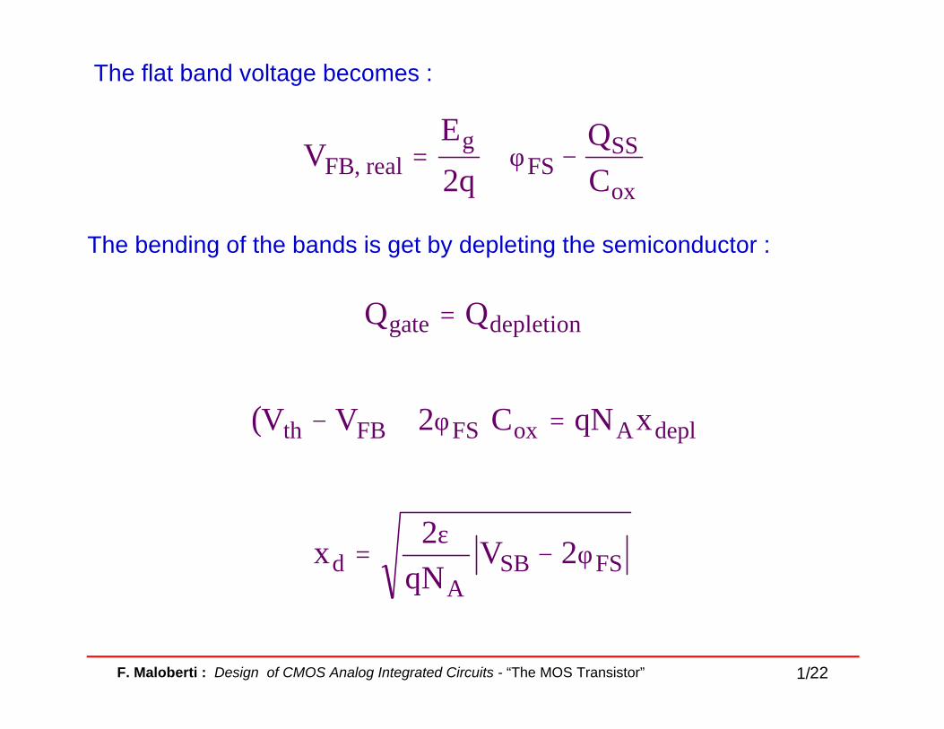
The flat band voltage becomes :
The bending of the bands is get by depleting the semiconductor :
ox
SSFS
greal,FB C
Q
q2
EV −φ+=
depletiongate QQ =
( ) deplAoxFSFBth xqNC2VV =φ+−
FSSBA
d 2VqN
2x φ−
ε=

F. Maloberti : Design of CMOS Analog Integrated Circuits - “The MOS Transistor” 231/
where γ is the body coefficient. If VSB = 0
The Threshold voltage can be expressed as :
( )FSSB
ox
impSSFS
gTh 2V
C
q2
EV φ−γ+
+−φ−=
ox
A
C
Nq2 ε=γ
FSFSreal,FB0,Th 22VV φγ+φ−=
FSFSSB0,ThTh 22VVV φ−φ−γ+=

F. Maloberti : Design of CMOS Analog Integrated Circuits - “The MOS Transistor” 241/
I-V CHARACTERISTICS
– Weak inversion region VGS < VTh
– Linear (or Triode) VTh < VGS > VDS + VTh
– Saturation region VTh < VGS < VDS + VTh

F. Maloberti : Design of CMOS Analog Integrated Circuits - “The MOS Transistor” 251/
Weak inversion region :
The band diagram indicates that the structure in equivalent to two back toback p-n diodes where the saturation current depends on the barrier height.
nkT/qVnkT/qV0DS
BG eeII −=
[ ]kT/qVnkT/qVnkT/qV0DD
DSBG e1eeII −− −=

F. Maloberti : Design of CMOS Analog Integrated Circuits - “The MOS Transistor” 261/
Linear (or Triode) region :
The voltage exceeding thethreshold determines anaccumulation of mobile charge onthe channel (inversion region)
V(x) is the drop voltage from source to x.
The resistance of an incremental element x, x + dx in the channel is :
The drop voltage across the element is :
)x(V)x(VVC)x(Q ThGSoxinv −−=
W)x(Q
dx
A
dxdR
inv µ=
σ=
W)x(Q
dxIdRIdV
inv
DD µ
==

F. Maloberti : Design of CMOS Analog Integrated Circuits - “The MOS Transistor” 271/
VTh changes along the channel due to the body effect :
We get :
if the second term can be neglected
FSSBFS0,ThTh 2)x(VV2VV φ−−+φ−γ+=
dxVVL
0DS ∫ ∆=
( ) [ ]
φ−−φ−+−φγ−−µ= 2/3
FDB2/3
FSB2DSDSF0,ThGSoxD 2V2V
3
2V
2
1V2VV
L
WCI
( )
−−
µ= 2
DSDSThGSoxD V2
1VVV
L
WCI

F. Maloberti : Design of CMOS Analog Integrated Circuits - “The MOS Transistor” 281/
Saturation region :
As V(x) increases Qinv(x) decreases. Its minimum is at the drain
Qinv(L) = Cox [ VGS - VTh - VDS ]
if
VDS = Vsat = VGS - VTh
Qinv(L) = 0
the drain is in the pinch-off condition.If VDS > Vsat, the pinch-off point moves toward the source; the part of the VDS
voltage exceeding Vsat drops along the depleted region, ∆L, extending fromthe pinch-off to the drain.
( )satDSA
VVqN
2L −
ε=∆

F. Maloberti : Design of CMOS Analog Integrated Circuits - “The MOS Transistor” 291/
The structure can be assumed equivalent to a transistor with the pinch-off at the drain but with length reduced of ∆L. It results :
having neglected Vsat with respect of VDS
λ = channel length modulation parameter 12 V105 −−⋅≈
A
7
A2 NL
10
NqL≅
ε=λ
( )( ) DSsatDS2
AsatDS2
A
V1VVLqN
1
VVLqN
21
1
LL
Lλ+≅−
ε+=
−ε
−=
∆−
( ) ( )LL
LVV
L
WC
2
1VV
LL
WC
2
1I 2
ThGSox2
ThGSoxD ∆−−µ=−
∆−µ=
F. Maloberti : Design of CMOS Analog Integrated Circuits - “The MOS Transistor” 301/
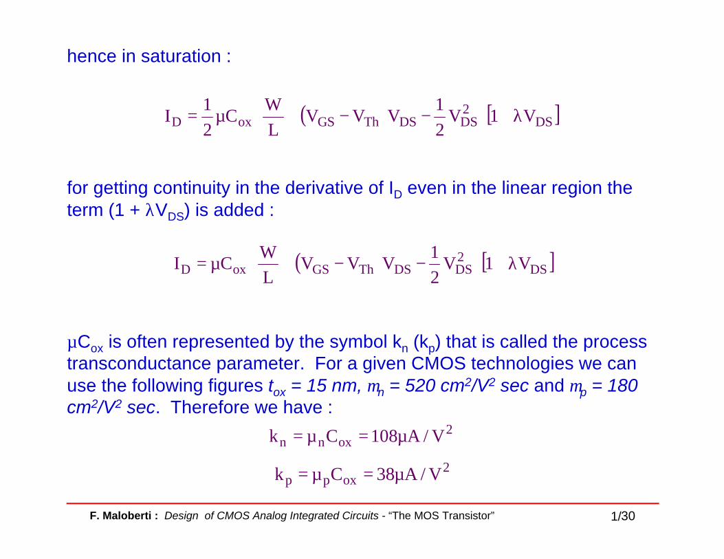
hence in saturation :
for getting continuity in the derivative of ID even in the linear region theterm (1 + λVDS) is added :
µCox is often represented by the symbol kn (kp) that is called the processtransconductance parameter. For a given CMOS technologies we canuse the following figures tox = 15 nm, µn = 520 cm2/V2 sec and µp = 180cm2/V2 sec. Therefore we have :
2oxnn V/A108Ck µ=µ=
( ) [ ]DS2DSDSThGSoxD V1V
2
1VVV
L
WCI λ+
−−
µ=
( ) [ ]DS2DSDSThGSoxD V1V
2
1VVV
L
WC
2
1I λ+
−−
µ=
2oxpp V/A38Ck µ=µ=

F. Maloberti : Design of CMOS Analog Integrated Circuits - “The MOS Transistor” 311/
LARGE SIGNAL EQUIVALENT CIRCUIT
Non linear Linear (1st approximation)
- Current source - Resistors
- Diodes - CGS, ov ; CGD, ov
- CGS, CBG, CGD, CBS, CBD

F. Maloberti : Design of CMOS Analog Integrated Circuits - “The MOS Transistor” 321/
• Typically :
•
• Diodes reversely biased; the reverse current is dominated by generation recombination term
A : area of the junction
xj : depletion region width
τo : mean lfetime for minority carriers
IGR doubles for an increase of 10
K typically at room temperature
IGR/A = 10-15 A/µm2.
0
jiGR 2
xqnAI
τ=
Ω−≈≈ 5010RR SD
oxovov,GDov,GS CWxCC ==

F. Maloberti : Design of CMOS Analog Integrated Circuits - “The MOS Transistor” 331/
SMALL SIGNAL EQUIVALENT CIRCUIT
Obtained by a linearization of the large signal equivalent circuit.
The linearization of the current source ID = ID (VGS, VDS, VBS)
generate three voltage controlled
current sources :
gm = δID/δVGS
transconductance
gds = δID/δVDS
drain output conductance
gmb = δID/δVBS
substrate transconductance

F. Maloberti : Design of CMOS Analog Integrated Circuits - “The MOS Transistor” 341/
Transconductance :
• In the subthreshold region (like a bipolar transistor) :
• In the linear region :
• In the saturation region :
qkT
n
Igg D
mbm ==
DSoxm VL
WCg
µ=
( ) ( ) DoxThGS
DThGSoxm I
L
WC2
VV
I2VV
L
WCg
µ=
−=−
µ=

F. Maloberti : Design of CMOS Analog Integrated Circuits - “The MOS Transistor” 351/
In the real situation gm is smallerthan the value predicted by thegiving simple equation. Moreovergm changes because of thedependence of µ from thetemperature, the trasversal and themean lateral electric field.
SPICE uses a fitting equation :
+
+
µ=µ
−−
sat
DS
m
crit
y23
00
LEV
1
1
E
E1
T
T
( )expu
DStraonGSox
sicrit0 VuVVC
u
−−−
ε⋅µ=µ

F. Maloberti : Design of CMOS Analog Integrated Circuits - “The MOS Transistor” 361/
Drain output conductance (gds) :
• In the linear region
• In the saturation region (first order)
•Second order effects
• The channel length reduction has been calculated taking into account only the lateral drop voltage. A more accurate analysis gives :
( )DSThGSoxds VVVL
WCg −−
µ=
Dds Ig λ=
( )( ) ( )
−
−β+−αε
+∆
≅∆ satDS
satGSGSDS
S
oxst VV
VVVVC
order1L
1
L
1

F. Maloberti : Design of CMOS Analog Integrated Circuits - “The MOS Transistor” 371/
• The threshold voltage depends on the VDS (short channel)
• The mobility depends on the lateral mean field VDS/L
• The avalanche effect increases ID.
Avalanche current :
Mobile charges, accelerated by electric field in the drain depleted region,creates, by impact ionization, electron-holes pair.

F. Maloberti : Design of CMOS Analog Integrated Circuits - “The MOS Transistor” 381/
• It appears an increase of the drain current ID and a substrate current IB
• The substrate current may contribute to latch-up
• The device noise increases
• The output impedance decreases
• Carriers can be trapped on the oxide and the VTh changes (hot electron effect)

F. Maloberti : Design of CMOS Analog Integrated Circuits - “The MOS Transistor” 391/
• Avalanche current worse in n-channel
More accurate expression of the output conductance :
(first order) (short channel) (velocity saturation) (avalanching)
DS
S
DS
D
DS
ThmDds V
I
V
I
V
VgIg
δδ
+δ
δµ⋅
µ+
δδ
⋅−λ=
F. Maloberti : Design of CMOS Analog Integrated Circuits - “The MOS Transistor” 401/
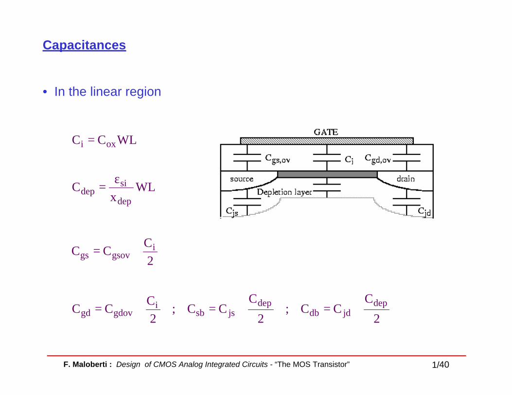
Capacitances
• In the linear region
WLCC oxi =
WLx
Cdep
sidep
ε=
2
CCC i
gsovgs +=
2
CCC;
2
CCC;
2
CCC dep
jddbdep
jssbi
gdovgd +=+=+=

F. Maloberti : Design of CMOS Analog Integrated Circuits - “The MOS Transistor” 411/
• In the saturation region
gdovgd CC ≅
3
C2CC dep
jssb +=
igbjddb C10
1C;CC ≅=
=φ
φ−
≅2i
DT
T
0jj
n
NANln
q
KT;
V1
CC
3
C2CC i
gsovgs +=

F. Maloberti : Design of CMOS Analog Integrated Circuits - “The MOS Transistor” 421/
m
2nTh
g
1kT4
3
2
f
V=
∆
∫ =δ
∆=
2
1
f
f m
2nTh2
n BWg
kT4
3
2f
f
VV
Thermal noise :
Due to the finite output resistance ifreffered to the input, as shown infigure
for ID = 50 µA, (VGS - VTh) = 300 mV,VnTh = 5.6 nV/ Hz
If the bandwidth BW of the systemis f2 - f1 the input referred noisevoltage is :

F. Maloberti : Design of CMOS Analog Integrated Circuits - “The MOS Transistor” 431/
Flicker noise :
Due to the trapping and detrapping of carriers by surface states at differentenergy levels.
Modeled as :
Typically : @ 1 kHz with WL = 1000 µ2
αα=
∆ kox
2fD
2nf
CLf
KI
f
V
WL
1
Cf2
k
gCLf
kI
fg
i
f
V1kc
ox
f2m
kcox
2fD
2m
2nf
2nf ⋅
µ==
∆=
∆ +αα
1fSSf kN toalproportion k1 ≈≈α
znf
H
nV40V =

F. Maloberti : Design of CMOS Analog Integrated Circuits - “The MOS Transistor” 441/
The power of the flicker noise is concentrated at low frequency
Noise spectra for n-channel Boron implanted p-MOS hal and p-channel transistor low 1/f noise (buried channel)
µ=
∆= +∫
1
21kc
ox
ff
f
2nf2
n f
fln
WLC2
kdf
f
VV
1
2

F. Maloberti : Design of CMOS Analog Integrated Circuits - “The MOS Transistor” 451/
Avalanche noise :
Due to the statistical fluctuation in the number of carriers of the avalanchecurrent (shot noise)
If referred to the input :
if we compare thermal noise with avalanche noise, we have
AV
2nAV ql2
f
i=
∆
Dox
AV2m
2nAV
2nAV
ILW
C
ql
fg
i
f
V
µ
=∆
=∆

F. Maloberti : Design of CMOS Analog Integrated Circuits - “The MOS Transistor” 461/
we get comparable boise if ID/IAV is of the same order of (VGS - VTh)/(kT/q).
The avalanche current at VDS = 5 V can be of the order of 0.5 - 1 µA.
To minimize the Noise
Thermal noise :
• Use large gm (large W/L)
• Use low series resistance (connection and gate resistance)
( ) AV
D
ThGSAV
m
2nAV
2nTh
I
I
VVq
kT
3
8
ql2
kTg432
V
V⋅
−⋅==

F. Maloberti : Design of CMOS Analog Integrated Circuits - “The MOS Transistor” 471/
Flicker noise :
• Use large device area (WL)
• Use thin oxide (high Cox)
• Use “clean” technology (low NSS)
• Try to get burried channel
• Use p-channel devices
Avalanche noise :
• Reduce VDS
• Use of p-channel devices

F. Maloberti : Design of CMOS Analog Integrated Circuits - “The MOS Transistor” 481/
LAYOUTRules :
• Use poly connection only for signal, never for current because the
offset RI = 15 mV.
• Minimize the line length, especially for lines connecting high
impedance nodes (if they are not the dominant node).
• Use matched structure. If necessary common centroid arrangement.
• Respect symmetries (even respect power devices).
• Only straight-line transistors.
• Separate (or shield) the input from the output line, to avoid feedback.
• Shielding of high impedance nodes to avoid noise injection from the
• power supply and the substrate.
• Regular shape

F. Maloberti : Design of CMOS Analog Integrated Circuits - “The MOS Transistor” 491/
LAYOUT OF TRANSISTORSMOS transistor is a overlap of two rectangles : active area (not
protected, to originate the source and the drain) and polysilicon gate.
The key point to consider :
• parasitic resistance at source and
drain must kept as low as possible
• parasitic capacitances must be
minimized
• matching between paired elements
is very imporant

F. Maloberti : Design of CMOS Analog Integrated Circuits - “The MOS Transistor” 501/
• Use multiple contact. Many contacts placed close to one another
make the surface of metal connection smoother than when we use
only one contact; this prevents microcraks in metal;
• Splitting the transistor in a number of equal part connected in parallel
permits to reduce the area of each transistor and so reduces parasitic
capacitances by two; the one on the right reduces the parasitic
capacitances by four.

F. Maloberti : Design of CMOS Analog Integrated Circuits - “The MOS Transistor” 511/
Matching is very important when we design current mirrors and
differential pairs. Bad matching produces high offset.
Transistors with different orientation match badly (fig. A); moreover we
can suffer mismatch if the current in transistors flowing in opposite
direction (fig. b). In addition, we can effect a change in physical and
technological parameters in points of the chip that are relatively far away

F. Maloberti : Design of CMOS Analog Integrated Circuits - “The MOS Transistor” 521/
The best method of achieving good matching is shown in the following
figure :
• Each transistor is split in four equal parts interleaved in two by two’s.
So that for one pair of pieces of the same transistor we have currents
flowing in opposite direction.
• Any noisy signal affecting the substrate or the well should be sunk by
the biasing and should not affect the circuit itself.