design of energy efficicent cmos current comparator · keywords: analog cmos circuit design,...
TRANSCRIPT

International Research Journal of Engineering and Technology (IRJET) e-ISSN: 2395 -0056
Volume: 03 Issue: 12 | Dec -2016 www.irjet.net p-ISSN: 2395-0072
© 2016, IRJET | Impact Factor value: 4.45 | ISO 9001:2008 Certified Journal | Page 1149
Design of Energy Efficicent CMOS Current Comparator
Rajesh Kumar1, Prof. Sanjay Tembhurne2
1Electronics & Communication Engineering, G.H.Raisoni Academy of Engineering &Technology,
RTM Nagpur University, Nagpur, India.
Email:[email protected] 2 Professor, Dept. of Electronics & Communication Engineering, G.H.Raisoni Academy of Engineering &Technology,
RTM Nagpur University, Nagpur, India.
Email:[email protected]
---------------------------------------------------------------------***-------------------------------------------------------------------- Abstract- In high-speed high-resolution analog to digital
converters, comparators have a key role in quality of performance. High power consumption and delay is one of the drawbacks of these circuits which can be reduced by using suitable architectures. Many versions of comparator are proposed to achieve desirable output in sub-micron and deep sub-micron design technologies. Back to back inverter in the latch stage is replaced with dual-input single output differential amplifier. This topology completely removes the noise that is present in the input. The structure shows lower power dissipation and higher speed than the conventional comparator. In this paper, a new low-voltage continuous-time current comparator is presented. The main idea is to use the voltage follower as a key element for the comparator input stage. This configuration delivers a very low input resistance, which is mandatory for current-mode applications. Previous reported current comparators present a high-speed response; nevertheless, only few are suitable for low-voltage applications. Simulations and experimental results using the complementary MOS 0.18-µm technology are presented to demonstrate the circuit feasibility.
Keywords: analog cmos circuit design, current comparator, positive feedback, low power, high speed.
1. INTRODUCTION
Analog current-mode techniques are drawing strong
attention today due to their potential application in the
design of high-speed mixed-signal processing circuits in
low-voltage standard VLSI CMOS technologies.
Industrial interest in the field has been propelled by the
proposal of innovative ideas for filters [1] and data
converter design, demonstrated by IC prototypes in the
video frequency range. Also current-mode circuits are
natural candidates for image sensory information
processing using novel neural and fuzzy signal
processing architectures [2].
A current comparator is intended to detect the
capability of a high impedance node to either source or
sink a current. Current sensing and comparison is
necessary for different applications. Current comparators
are basic building blocks for nonlinear current mode
signal processing and analog to digital converters. The
availability of large current ranges is an appealing feature
for both fields. Also, efficient small current level detection
is fundamental for high operation speed in high
resolution applications. Low level, high speed current
detection is also required in different light and radiation
sensing applications: for instance, γ-detectors using wide
band gap semiconductors, or controllability and re-
configurability issues in E-beam testing of integrated
circuits. For instance, in the latter the need arises to detect
current levels as low as 1nA in a few µs. Sub threshold
CMOS current mode massive computation architectures
also require efficient detection of low current levels for
fast discriminating function evaluation. To highlight
another application, current detection is also required in
IDDQ VLSI testing approaches [3].
The most common current comparator structure
follows the proposal of Freitas and Current in 1983,
where the input current is first sensed at a low-
impedance node and then amplified using a single-pole
voltage gain mechanism. We will call this architecture the
resistive-input comparator; it yields proper speed figures
for large current levels, but is somewhat inaccurate. An
alternative structure uses a high-impedance node at the
sensing front-end -capacitive-input comparator. This
obtains enlarged resolution, at the cost of increasing
voltage excursions at the input node and consequently,
decreasing the operation speed [4]. Recently, an
advanced current comparator architecture which uses
nonlinear feedback to combine advantages of the
capacitive and the resistive input architectures has been
proposed quasi-simultaneously by the authors, and Traff,
and demonstrated with CMOS circuits by the authors [5].
However, clear justifications of the merits of the different
architectures or criteria for optimum design still lack.
This paper aims to provide these justifications and
International Journal Of Advancements In Research & Technology, Volume 2, Issue 9, December-2016
ISSN 2278-7763
© 2016, IRJET | Impact Factor value: 4.45 | ISO 9001:2008 Certified Journal | Page 1150
criteria by focusing on the topic of CMOS current
comparator design from a fundamental point of view,
based on the use of simplified, conceptual models [6].
This fundamentalist development evolves into two
practical CMOS circuit structures which obtain resolution
and offset of pmos in the comparison function about
three orders of magnitude better than that attained with
conventional methods. One of these structures relies on
current switching, similar to the proposal in, [7], and
obtains a linear transient evolution dominated by a Miller
capacitance. The other, called current steering
comparator, uses a different principle to reduce Miller
effect and thus obtains better transient response
(quadratic instead of linear) while preserving the high-
resolution feature. However, the former structure is
simple to modify to route rectified versions of the input
current to a high-impedance output node -this cannot be
achieved using the current steering comparator [8].
Consequently, each structure yields specific advantages
over the other, depending on the application context.
Current steering structure is advantageous for pure
comparison, i.e., to codify the sign of the input current in
binary form, as is required for analog-to-digital
conversion. The other is advantageous for applications
where both the sign of the input current and the input
current itself are significant to the circuits operation -as in
function generation [9].
2. CURRENT COMPARATORS
Current comparators are very important for analog
circuit design because of their low power consumption,
minimum size transistors, high speed, small chip area
and many signal sources of sensors are current based.
Comparators are widely used in many analog to digital
converters and sensor circuit as well, particularly for
front-end signal processing applications and increasingly
within electronic systems [10]. Over past years, several
design approaches had been reported to reduce input
impedance. A simple current comparator has low
impedance input stage, high output impedance to
amplify small current difference. Operating frequency is
limited by high output impedance [11]. Current
comparator does not compensation for charge-injection
and offset voltage. Advanced current comparators may
preferably be used for portable wireless communication.
Fig. 1 shows the basic block diagram of the comparator.
Figure 1. Block diagram of three stage comparator[3]
The first high-speed, low input impedance current
comparator with common-drain input stage and positive
feedback loop of CMOS inverter allows low input
impedance was reported by Traff [12]. The circuit,
however, has a dead-band region in which the input
impedance is very large while lower input current and
thus increasing the response time. In order to shorten the
response time increased by dead-band problem, an
improved approach had been proposed as shown in Fig.
2. In Fig. 2, to shorten the response time, two CMOS
inverters are inserted in the feedback loop with a shunt
loop consists of a resistor and a capacitor which
compensates frequency response. Although the response
time and input impedance are improved, the added
inverters do not have rail-to-rail voltage swing during
low input current region and thus increasing power
consumption. That is, these current comparators are fit
for small current detection such as in photo-sensor
applications.
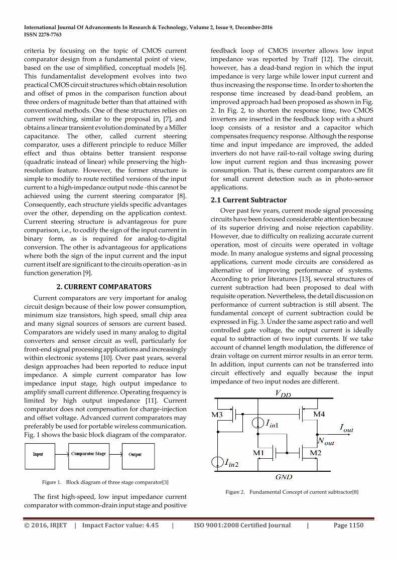
2.1 Current Subtractor
Over past few years, current mode signal processing
circuits have been focused considerable attention because
of its superior driving and noise rejection capability.
However, due to difficulty on realizing accurate current
operation, most of circuits were operated in voltage
mode. In many analogue systems and signal processing
applications, current mode circuits are considered as
alternative of improving performance of systems.
According to prior literatures [13], several structures of
current subtraction had been proposed to deal with
requisite operation. Nevertheless, the detail discussion on
performance of current subtraction is still absent. The
fundamental concept of current subtraction could be
expressed in Fig. 3. Under the same aspect ratio and well
controlled gate voltage, the output current is ideally
equal to subtraction of two input currents. If we take
account of channel length modulation, the difference of
drain voltage on current mirror results in an error term.
In addition, input currents can not be transferred into
circuit effectively and equally because the input
impedance of two input nodes are different.
Figure 2. Fundamental Concept of current subtractor[8]

International Journal Of Advancements In Research & Technology, Volume 2, Issue 9, December-2016
ISSN 2278-7763
© 2016, IRJET | Impact Factor value: 4.45 | ISO 9001:2008 Certified Journal | Page 1151
To deal with error terms of current subtraction [14], a
current subtractor with balanced input stages was
proposed for the application of nonlinear switched-
current circuit. With balanced low input impedance, the
input currents are transferred into circuit equally which
effectively reduce subtraction error. However, the
mismatching drain-source voltage of current mirror
originated from channel length modulation is still
evident that degenerates the accuracy of subtraction [8]. If
the subtraction error is out of tolerance of application, the
faulty occurrence may affect the performance and bring
the system into collapse the worst. We thus require a
precise current subtractor to enhance the reliability of its
application
2.2 Current Comparator Specification
The current comparator function is to detect the sign
of an input current, to provide an output signal (voltage
or current) which codifies this sign in binary form. This
paper focuses on trans impedance structures [15].
Current transfer structures are obtained by cascading the
former with voltage-controlled current switches, which
can be built using for instance a differential amplifier.
Figure 3. Ideal current comparator operation[11]
Fig.4 shows the ideal current comparator transfer
characteristics for voltage codification. EOL and EOH in
this figure denote the boundary values for the output
logical states; Fig.4 shows the ideal comparator transient
response. These figures illustrate the ideal current
comparator features: a) infinite trans impedance in the
transition region; b) zero offset; and c) zero delay [16].
Also, to reduce loading errors due to finite output
resistance of the driving source, the input voltage of an
ideal current comparator should be kept constant for the
full range of input current. Finally, all these
characteristics should hold true for the largest possible
input current range. Practical circuit performance
deviates from these ideal features, and is characterized by
a set of static and dynamic specification parameters,
among which the most significant for design are: l offset
(Ios), defined as the input current required to annul the
output voltage, l gain error, (∆), or static resolution,
defined as the input increase needed to drive the output
voltage from EOL to EOH; any input level larger than
static resolution is called an overdrive, l resolution time
(TR), defined as the time required for the output to
change from 0 up to EOH (or down to EOL), following
the application of an overdrive input step, and l response
time (TD), defined as the time required for the output to
change between the two logical states, following an input
edge between two opposite-sign overdrive levels.
Figure 4. High resolution CMOS current comparator[9]
A. High-Resolution CMOS Current Comparators:
Current-Switch vs. Resistive-Input [17] Fig.5 shows the
schematics of a CMOS prototype of the resistive-input
comparator of Fig.5, for a single-poly n-well 2µm
technology. Cascode transistors are used to increase the
amplifier voltage gain. Also, a CMOS inverter has been
added to drive pad load and regenerate output voltage
logic levels. The schematics for a current switching
prototype, according to the concept of Fig.5, is shown in
Fig.5. The amplifier of this circuit is built by using a
simple CMOS inverter; an inverter is also used for
buffering.

International Journal Of Advancements In Research & Technology, Volume 2, Issue 9, December-2016
ISSN 2278-7763
© 2016, IRJET | Impact Factor value: 4.45 | ISO 9001:2008 Certified Journal | Page 1152
Figure 5. Resistive input current comparator[5]
High resolution CMOS current comparators [18] can
be implemented using very simple circuits, based on a
fundamental knowledge of the mechanisms underlying
the operation of this block. It requires using nonlinear
characteristics with well-controlled breakpoints and
sharp transitions, which are better realized using
feedback structures. Also, the self-tracking provided by
these feedback structures guarantees robust high
resolution (<1pA) and low offset (<1pA) operation in a
standard VLSI CMOS technology.
The core current switch comparator circuit is extended
in a simple manner to define a family of high resolution
nonlinear current-mode circuits with applications in
sensor signal conditioning, artificial neural networks, and
fuzzy interpolation systems. The proposed circuit also
shows potential use as the second stage in voltage
comparators, to reduce the propagation time required to
remove the charge accumulated in this stage input
capacitor [19].
3. PROPOSED DESIGN
Figure 6. Proposed High Speed Low Power Current Comparator
Fig 7 above shows the novel current comparator
structure. The input resistance of the new structure,
shown in Fig. 7, is approximately l/gm. The purpose of
using a source follower input stage is, in addition to low
resistance, the ability of applying feedback to the gates.
To achieve sufficient gain for amplifying small voltage
variations at the input stage node, positive voltage
feedback from a CMOS inverter is used. As for the
current mirror comparator, short transition times and
clocked rail-to-rail slewing is achieved by connecting
additional cascaded CMOS inverters to the output (Fig.
7). By introducing a simple MOS switch between the
CMOS inverters and the output of the comparator, a
clocked differential output is also obtained. This output
stage has desirable properties and should preferably he
used for better performance. One consequence of the low
input resistance is that simpler current mirrors can he
used to provide current subtraction to the input node. In
Fig. 4a the potentials at the input and output nodes are
shown. Obviously one of the input transistors is always
non conducting owing to the positive feedback biasing
from the inverter stage.
One disadvantage of the novel approach concerns the
input voltage to the positive feedback inverter. It does not
slew from rail to rail, making neither M3 nor M4 totally
shutoff. Thereby a quiescent current will flow, giving rise
to a nonzero DC power dissipation. However, there is no
quiescent current in the input stage.

International Journal Of Advancements In Research & Technology, Volume 2, Issue 9, December-2016
ISSN 2278-7763
© 2016, IRJET | Impact Factor value: 4.45 | ISO 9001:2008 Certified Journal | Page 1153
4. RESULTS
Simulation results of the proposed design show that
power consumption is approximately 4.67mW when
implemented using a 180nm CMOS process. The gain of
the comparator is found to be approximately 4.5e6. The
input impedance is 15.8e3 and the output impedance is
18.1e3 ohms respectively.
Figure 7. Transient analysis simulation waveforms
The DC analysis of the proposed design shows that
the proposed design allows for almost rail to rail output
swing ranging from 0.5V to 4.5V. The comparator delay
improves steadily as we move from 250nm process to
180nm and down to 130nm.
Figure 8. DC analysis waveform
Results of analysis of the proposed design are
compared with previous designs found in the literature.
This comparison is tabulated below in table 1.
Table1 Comparative Results
Design Power(W) Delay(s) Process(nm)
[10] 2015 6.9m 9.5n 180
[9] 2015 1.8m 16n 180
[15] 2009 5.3m 12n 180
Proposed 4.6m 10n 180
The results above show that we are able to achieve
low delay despite using a 180nm process while the other
reference designs were based on the 180nm process.
Also, power consumption is very low, again despite
using an 180nm technology process. Thus, our 180nm
based design achieves the best power-delay product
when compared to similar state of the art designs in the
literature.
5. CONCLUSION
A CMOS current comparator circuit, realizable in any
standard CMOS process, has been presented and its
performance discussed. Propagation delays through the
loaded comparator circuit were simulated to be about 10
ns for threshold current levels between 5 and 25 uA. The
high comparator gains were shown through simulation
to provide high levels of logical discrimination. Current
comparators of this type may allow the designers of
CMOS VLSI circuits with both analogue and digital
functions greater design flexibility through the use of
analogue current summing and threshold detection.
6.FUTURE SCOPE
The proposed design may be further refined in terms of power dissipation, gain, input impendance, and delay. Many of
these parameters can be improved simply by moving to a
smaller feature size technology, such as 130nm and
lower. Moving to a smaller technology causes
deterioration in gain as the MOSFET transimpedance is
lower for smaller devices. In order to overcome the loss
in gain, additional gain stages may be added to the
comparator.
References [1] Freitas, D.A., Current, K.W., CMOS Current
Comparator Circuit, IEEE Electronics Letters, Vol. 19, No. 17, August 18, 1993.
[2] Traff, H., Novel Approach to High Speed CMOS Current Comparators, IEEE Electronics Letters, Vol. 28, No. 3, 30 January 1992.
[3] Tang, A.T.K., Toumazou, C., High Performance CMOS Current Comparator, IEEE Electronics Letters, Vol. 30, No. 1, 6 January 1994.
[4] Palmisano, G., Palumbo, G., High Performance CMOS Current Comparator Design, IEEE

International Journal Of Advancements In Research & Technology, Volume 2, Issue 9, December-2016
ISSN 2278-7763
© 2016, IRJET | Impact Factor value: 4.45 | ISO 9001:2008 Certified Journal | Page 1154
Transactions on Circuits and Systems-II: Analog and Digital Signal Processing, Vol. 43, No. 12, December 1996.
[5] Linan-Cembrano, G.,Del Rio-Fernandez, R., Dominguez-Castro, R., Rodriguez-Vazquez, A., Robust High Accuracy High Speed Continuous Time CMOS Current Comparator, IEEE Electronics Letters, Vol. 33, No. 25, 4 December 1997.
[6] Ravezzi, L., Stoppa, D., Dalla Betta, G.F., Simple High Speed CMOS Current Comparator, IEEE Electronics Letters, Vol. 33, No. 22, 23 October 1997.
[7] Jankatkit, T., Kasemsuwan, V., Low Voltage Current Mode Preamplifier Based Latch Comparator, IEEE Conference on Analog Design, 2016.
[8] Solis, J.E.M., Navarro, M.G., Mejia, I., Low Input Resistance CMOS Current Comparator, IEEE Canadian Journal of Electrical and Computer Engineering, Vol. 39, No.2 Spring 2016.
[9] Saxena, S., Akashe, S., Design of Low Leakage Current Average Power CMOS Current Comparator, IEEE Fifth International Conference on Advanced Computing and Communication Technologies, 2015.
[10] Vanitha, R., Thenmozhi, S., Low Power CMOS Comparator using BiCMOS, IEEE International Conference on Electronics and Communication Systems, 2015.
[11] Sarkar, S., Banerjee, S., 500 MHz Differential Latched Current Comparator, Proceedings of the IEEE Students Technology Symposium 2014.
[12] Chasta, N., Very High Speed High Resolution Current Comparator, World Academy of Science, Engineering, and Technology (WASET), International Journal of ECE Engineering, Vol. 7, No. 11, 2013.
[13] Thrivikramaru, V., Baghel, R.K., High Speed Low Power CMOS Current Comparator, IEEE International Conference on Communication Systems, 2012.
[14] Choudhary, R., Bhardwaj, M., Design of Low Power Low Input Impedance CMOS Current Comparator, IEEE Second International Conference on Advanced Computing and Communication Technologies, 2012.
[15] Tang, X., Pun, K.P., High Performance CMOS Current Comparator, IEEE Electronics Letters, Vol. 45, No. 20, 24 September 2009.
[16] Banks, D., Toumazou, C., Low Power High Speed CMOS Current Comparator, IEEE Electronics Letters, Vol. 44, No. 3, 31 January 2008.
[17] Weng, R.M., Chiang, C.W., Low Power High Speed Current Latched Comparator, IEEE Asia Pacific Conference on Circuits and Systems, December 6-9, 2004.