design of modular power management and attitude control
TRANSCRIPT

Research ArticleDesign of Modular Power Management and Attitude ControlSubsystems for a Microsatellite
Anwar Ali ,1 Shoaib Ahmed Khan,2 M. Usman Khan,2 Haider Ali ,1 M. Rizwan Mughal,3,4
and Jaan Praks4
1Electrical Technology Department, University of Technology (UoT), Nowshera, Pakistan2National University of Computer & Emerging Sciences Peshawar Campus, Pakistan3Department of Electrical Engineering, Institute of Space Technology, Islamabad, Pakistan4Department of Electronics and Nanoengineering, School of Electrical Engineering, Aalto University, FI-00076 AALTO,02150 Espoo, Finland
Correspondence should be addressed to Anwar Ali; [email protected]
Received 16 February 2018; Accepted 29 August 2018; Published 17 December 2018
Academic Editor: Jeremy Straub
Copyright © 2018 Anwar Ali et al. This is an open access article distributed under the Creative Commons Attribution License,which permits unrestricted use, distribution, and reproduction in any medium, provided the original work is properly cited.
The Electric Power System (EPS) and attitude control system (ACS) are the essential components of any satellite. EPS and ACSefficiency and compactness are substantial for the proper operation and performance of the satellite’s entire mission life. So,realizing the significance of EPS and ACS subsystems for any satellite, they have been assimilated and developed in modularforms focusing on efficiency and compactness. The EPS is comprised of three modules called the solar panel module (SPM),power conditioning module (PCM), and power distribution module (PDM) while the ACS has an embedded magnetorquer coil.For compactness and miniaturization purposes, the magnetorquer coil is embedded inside the SPM. The components used arecommercial off-the-shelf (COTS) components emphasizing on their power efficiency, small dimensions, and weight. Latch-upprotection systems have been designed and analyzed for CMOS-based COTS components, in order to make them suitable forspace radioactive environment. The main design features are modularity, redundancy, power efficiency, and to avoid singlecomponent failure. The modular development of the EPS and ACS helps to reuse them for future missions, and as a result, theoverall budget, development, and testing time and cost are reduced. A specific satellite mission can be achieved by reassemblingthe required subsystems.
1. Introduction
Many universities around the world are working on variousprojects of small satellites [1–6]. These satellites are classifiedinto various categories on the basis of their mass and dimen-sions, i.e., pico, nano, and micro. The main driving forcefor the development of small satellites is their low budgetrequirement, short development time, low mass and size,new technology, and because they provide more cost-effective and reliable access to space [7]. Small satellites aredesigned for low earth orbit (LEO); therefore, launching costis also comparatively low. Small satellites can provide an idealtestbed to innovative technologies (e.g., hardware and soft-ware) which can be further used in large and expensive spacemissions. University satellite programs teach students the
whole lifecycle of a satellite on a real situation and developtheir capabilities in the space sector. Due to mentioned facts,small satellites have been considered a vital technology bymany space mission experts.
The number of student-built small satellites is rapidlygrowing, specifically in Europe and in North America. Thelist of the number of universities working on satellite projectsis too long, and it is impossible to mention all of them here.But some of the universities that are particularly movingthe small satellite industry forward and working on very niceprojects are mentioned here. From the United States ofAmerica, the significant contribution is from Cal Poly andStanford University, University of Michigan, University ofTexas, Air Force Academy, Massachusetts Institute of Tech-nology, Colorado University Boulder, Santa Clara University,
HindawiInternational Journal of Aerospace EngineeringVolume 2018, Article ID 2515036, 13 pageshttps://doi.org/10.1155/2018/2515036

Arizona State University, and many more [8, 9]. FromEurope, the contribution worth mentioning is from theSwedish Institute of Space Physics, Aalborg University,Technical University of Denmark, Norwegian Universityof Technology and Science (NTNU), University of Wurz-burg, Aachen University of Applied Sciences, Delft Univer-sity of Technology, Swiss Federal Institute of Technology(EPFL), Budapest University of Technology and Economics,University of Montpellier II, Warsaw University of Technol-ogy, Sapienza University of Technology, University of Vigo,Polytechnic University of Turin, Berlin Technical University,the Space Research Centre of Polish Academy of Sciences,and a lot of other institutions. In Asia, the main contributinguniversities are from Japan, China, South Korea, Singapore,and India [9].
Keeping in view the significance of small satellites, thePakistan National Space and Upper Atmospheric ResearchCorporation (SUPARCO) has framed the Pakistan NationalStudent Satellite (PNSS) program [10]. This program willinvolve the local universities and industry in collaborationwith SUPARCO for the development and launching of smallsatellites into space. In this program, PNSS-1 is the first smallsatellite that will be deployed into space. Universities are partof the designing process of the satellite. The main aim of thiswork is to design and analyze modular EPS and ACS for thePNSS-1 satellite which has a size of 50 cm3 with 50 kg massand one-year service life [11].
The EPS is responsible for fulfilling the power needs ofthe entire satellite. The paper proposes a novel approachto design and elegantly interconnect the EPS subsystemsof a modular small satellite [12]. In the proposed modulardesign technique, the EPS is divided into small modulesthat are designed and developed independently and areattached together to attain the intended results. The majorsubsystems of the EPS are the solar panel subsystem, con-version of the solar panel power to the power distributionbus (PDB) level subsystem, and conversion of the unregu-lated PDB voltage level into various low voltage levelsrequired for operation of the satellite subsystem compo-nents. The EPS also has a subsystem to store the excessgenerated power into onboard batteries and extract powerfrom them during satellite night and solar eclipses. Differ-ent housekeeping sensors are embedded in the EPS sub-systems to monitor and ensure the proper operation ofthe complete satellite. To perform all the abovementioned
tasks, the whole EPS is subdivided into three modulescalled the solar panel module (SPM), power conditioningmodule (PCM), and power distribution module (PDM).This modular design approach is not only cost effectivebecause the design, development, and testing costs areshared among these modules but also time saving becauseof the parallel development approach rather than the clas-sical serial one [13–16]. In addition, the modular designextensively results in overall cost reduction because the costis shared among many modules that can be used severaltimes in other missions.
Each module offers standardized power and data inter-faces. A block diagram of the EPS subsystems is depictedin Figure 1.
The SPM is responsible for the power generation ofPNSS-1. Four solar panels are attached on the outsideperiphery of the satellite accountable for power generation.One solar panel generates sufficient power to meet the powerneeds of the complete satellite. The SPM output power is notconstant and has variable voltage and current levels depend-ing on solar power density and environment factors. Thepower conditioning module (PCM) converts this unstableSPM output voltage to a stable PDB voltage level. The PCMoperates the solar panels at its maximum power point(MPP) to harvest maximum power. For this purpose, thePCM has four Maximum Power Point Tracking- (MPPT-)based converters. Each converter is connected to four solarpanels on the input side and regulates the battery chargeand discharge on the MPPT scheme on the output side.The functional requirements of the PCM are to generatethe PDB for the spacecraft at 28V± 6V from raw poweravailable from four body-mounted solar panels. The inputvoltage of the PCM may vary from 40V to 80V. The PCMis connected with the satellite onboard computer (OBC)through redundant CAN buses. It has an interface with allof the power sources (i.e., solar panels and battery) and out-puts the PDB to the power distribution module (PDM). ThePDM converts the PDB voltage level into lower specific volt-age levels and distributes them to loads as per their require-ments [17]. The PDM also has the EMI filtration as well asdifferent protections on each distribution line in order tolimit the electromagnetic noise on the main bus and preventfault propagation. The ON/OFF switching of all switchableloads is also implemented inside the PDM. These switchesare controllable through telecommands. The complete design
Power conditioningmodule(PCM)
Solar panelmodule(SPM)
Power distributionmodule(PDM)
Sate
ttlite
subs
yste
ms
Power bus Data bus
CANbus
CANbus
CANbus
CANbus
Satelliteon-boardcomputer
(OBC)
Figure 1: Block diagram of EPS subsystems.
2 International Journal of Aerospace Engineering

of the specific module is discussed in the respective section ofthis paper, in detail.
The ACS of the PNSS-1 is responsible for attitude controlas is obvious from its name. The ACS is responsible fororienting the satellite solar panels for harvesting maximumsolar power and the satellite antenna toward ground stationantennas. For the attitude control of small satellites, threetypes of systems are normally used, i.e., permanent magnet,reaction wheel, and magnetic rods. All the three systems havetheir pros and cons. For example, the permanent magnet isinexpensive, but its weight and pointing accuracy makes itincompatible with small satellites. Reaction wheels and mag-netic rods are more precise, but their high price, greaterweight, and large size are unacceptable for small satellites.In this paper, an innovative concept of an embedded magne-torquer coil is presented for the attitude control of small sat-ellites. The magnetorquer coil comprises four subcoilsembedded inside the four internal layers of an eight-layerPCB of the SPM module. This innovative design not onlyreduces cost and size of the magnetorquer unit but alsoresults in an almost weightless system.
The paper is organized according to the followingsequence. Section 1 provides the EPS introduction and Sec-tion 2 describes the design and analysis of the SPM subsys-tem. Section 3 discusses the design description of PCMsubsystems according to general constraints and explains indetail the design and simulations of a wide range inputMPPT-based buck converter. Section 4 describes the designdetails of the PDM, while the last, Section 5, discusses theresults and conclusions.
2. Solar Panel Module
Selecting the correct power ratings for the SPM is the mostimportant aspect of the photovoltaic (PV) system design fora microsatellite. The inappropriate string size will result inmany problems. Choosing a small string size will result insmall efficiency. Selecting a large string size will damage theconverter and the associated equipment [18]. Solar cells canbe connected in any fashion, i.e., series or parallel. Series con-nections increase the voltage with the current kept constantwhile parallel connections increase the current of the stringwith the voltage remaining constant. Calculating the stringsize, the relationship between ambient temperature andstring voltage must be taken into consideration. Ambienttemperature has adverse effect on PV array voltage output.Low temperatures result in increases to output voltage whilehigh temperatures decrease string voltage. Proper and accu-rate power analysis is essential to compute the power ratingsfor efficient SPM design [19].
Triple-junction GaAs solar cells are selected for thesolar panel design of PNSS-1. The single cell has a maxi-mum power point voltage (Vmp) of 2396mV and short cir-cuit current density (JSC) of 17.67mA/cm2 which gives0.42A current. According to the PNSS-1 solar panel designrequirement, a single solar panel should generate at least50W with maximum output voltage of 80V and minimumvoltage should not be less than 40V under normal sunlightconditions at sun incidence angle of 5°. It means that multiple
string arrays will be used for the solar panel design. The effi-ciency of the solar cell array is always less than the sum ofindividual cells because of the manufacturing issues andenvironmental factors, collectively called as the degradationfactor [20]. For the solar panel design calculations, it is essen-tial to take into account the degradation factor. The data ofthe required triple-junction GaAs solar cell for this designis given in Table 1.
For calculation of the minimum voltage limit of a singlesolar cell, the maximum temperature limit is applied, becauseas the temperature increases above the standard test condi-tions (STC), i.e., 25°C, the voltage reduces per degree rise intemperature. Let us assume that the maximum temperatureis 85°C. Difference between maximum temperature andSTC is 60°C which will reduce the single cell minimum volt-age to Vmin = 2 396 + 60 × −5 94 × 10−3 = 2 038V where−5.94× 10⁻³ is the change in open circuit voltage per degreechange in temperature ΔVoc/ΔT as given in Table 1. Afterapplying the degradation factor of 0.85, the resultant mini-mum voltage for the single cell becomes 1.732V.
For upper voltage limit calculation, minimum operat-ing temperature is considered. Let us assume that the mini-mum temperature is −45°C. Difference between minimumtemperature and STC is −70°C which will increase the singlecell maximum voltage to Vmax = 2 396 + −70 × −5 589 ×10−3 = 3 09V where −5.589× 10⁻³ is the change in MPPvoltage per degree change in temperature ΔVmp/ΔT asgiven in Table 1. After applying the degradation factor of0.85, the resultant maximum voltage becomes 2.63V.
From the degradation analysis given above, we can findthe minimum and maximum number of cells required toachieve the upper and lower voltage limits. The maximumnumber of the solar cell limit is found by dividing theupper voltage limit with the single cell maximum voltage,i.e., 80V/2 63V = 31, while the minimum number of therequired cell limit is found by dividing the lower voltage limitwith the single cell minimum voltage, i.e., 40V/1 73V = 23.
After applying the degradation factor, the single cell out-put current is 0.36A.
Table 1: GaAs triple-junction solar cell characteristics.
Type GalnP2/GaAs/GeCell dimension 39.8mm× 60.4mm
Short circuit current density Jsc,mA/cm2 17.67
Open circuit voltage Voc,mV 2700
Maximum power point current densityJmp,mA/cm2
17.13
Maximum power point voltage vmp,mV 2396
Fill factor (FF) 0.86
Efficiency (η) 30%
Change in open circuit voltage per degreechange in temperature ΔVoc/ΔT −5.589mV/°C
Change in maximum power point voltage perdegree change in temperature ΔVmp/ΔT −5.964mV/°C
3International Journal of Aerospace Engineering

According to the design requirements, the average outputpower from the solar panel should not be less than 50W.The power analysis shows that minimum required poweris 40W and maximum required power is 60W. Single cellaverage output power is 0.78W. The solar panel has dimen-sions of 470mm× 450mm, and single cell dimensions are39.8mm× 60.4mm. It means that a maximum of 87 solarcells can be accommodated on the solar panel. Excludingthe area required for the sun sensor, temperature sensor,and bypass diodes, the total number of cells that can beaccommodated on the solar panel is 64. These cells aredivided into two strings; each has 32 solar cells connectedin series. The average voltage of the single cell is 2.18V andmaximum numbers of solar cells are 32 which result in aver-age output voltage and current of 69V and 0.72A, respec-tively. The resultant output power after applying all thedegradation factors is 50W. A bypass diode is connected inparallel to each solar cell which ensures proper operation ofthe single cell if one of them is damaged. A protection diodeis added at the end of each string of 32 solar cells to protect itfrom reverse current flow.
For the SPM to operate within its temperature limits, aglass-protected NTC (negative temperature coefficient)thermistor is mounted onto the solar panel for protectionagainst transient voltage spikes. Output voltage of the sensoris linearly proportional to temperature. Its resistance rangevaries between 2.2 k and 100 k, which is highly accurate with1% of tolerance.
3. Power Conditioning Module (PCM)
The PCM is responsible for converting solar panels’ unstablevoltage (40V~80V) into a stable voltage level delivered to thePDB (28± 6V). It is also responsible for voltage regulation,
battery charging, and health monitoring of different PCMsubsystems. A MPPT-based buck converter is designed andsimulated to operate the solar panel at its MPP. To achievemaximum power point, the MPPT buck converter can bedesigned using different MPPT algorithms. Most commonalgorithms for recognition of MPP are the constant voltagemethod [21], short-current pulse method [22], open voltagemethod [23], perturb and observe method [24], and incre-mental conductance method [25]. These seven MPPT algo-rithms are examined and evaluated on the basis ofefficiency [26]. The perturb and observe method shows thebest result and better efficiency as compared to others [27,28]; therefore, this algorithm is chosen for the PCM MPPTdesign. Batteries are charged and discharged from the PDBthrough a battery charging system. The PCM controller isused to perform the power management and control opera-tions of the entire unit. It communicates with the OBC ofthe satellite using redundant CAN buses. PCM casing dimen-sions and input/output power/signal have standardized con-nectors which result in a fully modular system that can beattached and detached as a separate unit to the rest of the sat-ellite subsystems. Figure 2(a) shows the conceptual-levelblock diagram of the PCM subsystem while Figure 2(b)shows the PCB dimensions of the PCM. Casing dimensionsof the PCM are shown in Figure 3.
3.1. PCMDesign Description. The PCM consists of four mod-ular and redundant MPPT units and CAN controller. EachMPPT unit has a local microcontroller (MSP430) to whichdifferent subsystems like MPPT switching converter, current,voltage, and temperature sensors are connected. These con-trollers are CMOS-based COTS components which areprone to radiation. In order to protect them from radiationdamage, a latch-up protection system is designed for the
Batteries
Powerdistribution
unit
Loadswitch
Currentsensor
Voltagesensor
BiDirectional
currentsensor
Anti-latch-upprotection PCU
controller
Voltagesensor
Currentsensor
MPPTswitchingconverter
Solar panel
Solar panel
Solar panel
Solar panel
Primary power bus PCU2,PCU3,PUC4Power distribution
bus (PDB)
PCU-1 PCU-2 PCU-3 PCU-4
Temperaturesensor
CAN-1 CAN-2
+
−
(a)
(0,0)
100 mm
150
mm
3.2
3.2
10.8 Ø3.8
Ø3.8
Ø3.8
Ø3.8
4 SolarPanel _DB15
CAN_DB9Batteries_Charger_DB9 connector
MPPTboost converter,
over voltageprotection,
temperature,current & voltage
sensors
PCUcontroller,latch-up
protection andauxiliary
components
PCU_OutPut_DB9connector
1.66.46.69.0
9.15
8.3
Ground planes
0.4 mm
1.6 mm
Components
Layer-1
Layer-3Layer-4
Layer-2
(b)
Figure 2: (a) PCM block diagram and (b) PCB dimensions.
4 International Journal of Aerospace Engineering

PCM unit. The four MPPT controllers (MSP430) and CANcontroller (PIC24HJ256GP10) are communicating with eachother through SPI protocol while the CANmicrocontroller iscommunicating with the OBC of the satellite through anembedded CAN transceiver system having redundant CANbuses. A schematic of the PCM is shown in Figure 4.
In the PCM design, the perturb and observe algorithm isopted to continuously locate the maximum power point andextract maximum power from the solar panels connectedwith it. The P&O algorithm works by continuously calculat-ing the power (current and voltage) from PV arrays and com-paring it with preceding calculated power values. If there is adifference and the power calculated from the current cycle isgreater than the previous cycle, the controller moves the
MPP in that direction by increasing the duty cycle; otherwise,if the power levels are same, it is the maximum power point[27]. Current, voltage, and temperature sensors ensureproper voltage, current, and temperature limits of the solarpanel output and on the PDB level. One set of voltage andcurrent sensors is connected at the output of the solar panel(input of the buck converter) in all four redundant MPPTunits, and a second set of current and voltage sensors is con-nected at the output of the buck converter. A bidirectionalcurrent sensor is employed at the input of batteries to moni-tor the battery charging and discharging currents. Latch-upprotection and watchdog timer blocks protect the MPPTlocal controller of each unit from single-event latch-ups. Asingle MPPT buck converter unit is shown in Figure 5.
Inlet for the solar panelconnector
50 m
m
160 mm 110 mm
Outlet for the powerdistribution bus (PDB)
connector
Outlet for the CANconnector-1
Outlet for the CANconnector-1
Figure 3: Casing dimensions of the PCM.
MPPT based buckconverter unit-1
MPPT based buckconverter unit-2 MPPT based buck
converter unit-3
MPPT based buckconverter unit-4
PCM maincontroller
PCM input from SPM
PCM output toPD
M
Output tobatteries
Figure 4: PCM complete schematic.
5International Journal of Aerospace Engineering
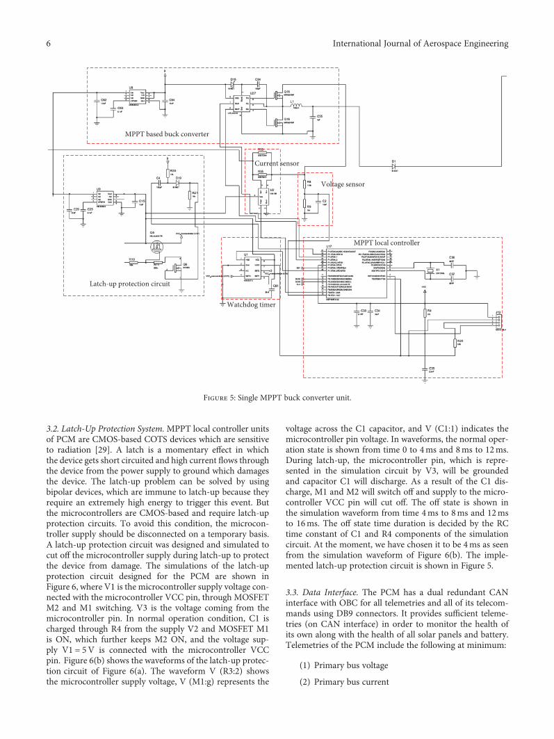
3.2. Latch-Up Protection System.MPPT local controller unitsof PCM are CMOS-based COTS devices which are sensitiveto radiation [29]. A latch is a momentary effect in whichthe device gets short circuited and high current flows throughthe device from the power supply to ground which damagesthe device. The latch-up problem can be solved by usingbipolar devices, which are immune to latch-up because theyrequire an extremely high energy to trigger this event. Butthe microcontrollers are CMOS-based and require latch-upprotection circuits. To avoid this condition, the microcon-troller supply should be disconnected on a temporary basis.A latch-up protection circuit was designed and simulated tocut off the microcontroller supply during latch-up to protectthe device from damage. The simulations of the latch-upprotection circuit designed for the PCM are shown inFigure 6, where V1 is the microcontroller supply voltage con-nected with the microcontroller VCC pin, through MOSFETM2 and M1 switching. V3 is the voltage coming from themicrocontroller pin. In normal operation condition, C1 ischarged through R4 from the supply V2 and MOSFET M1is ON, which further keeps M2 ON, and the voltage sup-ply V1 = 5V is connected with the microcontroller VCCpin. Figure 6(b) shows the waveforms of the latch-up protec-tion circuit of Figure 6(a). The waveform V (R3:2) showsthe microcontroller supply voltage, V (M1:g) represents the
voltage across the C1 capacitor, and V (C1:1) indicates themicrocontroller pin voltage. In waveforms, the normal oper-ation state is shown from time 0 to 4ms and 8ms to 12ms.During latch-up, the microcontroller pin, which is repre-sented in the simulation circuit by V3, will be groundedand capacitor C1 will discharge. As a result of the C1 dis-charge, M1 and M2 will switch off and supply to the micro-controller VCC pin will cut off. The off state is shown inthe simulation waveform from time 4ms to 8ms and 12msto 16ms. The off state time duration is decided by the RCtime constant of C1 and R4 components of the simulationcircuit. At the moment, we have chosen it to be 4ms as seenfrom the simulation waveform of Figure 6(b). The imple-mented latch-up protection circuit is shown in Figure 5.
3.3. Data Interface. The PCM has a dual redundant CANinterface with OBC for all telemetries and all of its telecom-mands using DB9 connectors. It provides sufficient teleme-tries (on CAN interface) in order to monitor the health ofits own along with the health of all solar panels and battery.Telemetries of the PCM include the following at minimum:
(1) Primary bus voltage
(2) Primary bus current
MPPT based buck converter
Latch-up protection circuit
Watchdog timer
Current sensor
Voltage sensor
MPPT local controller
Figure 5: Single MPPT buck converter unit.
6 International Journal of Aerospace Engineering

(3) Battery charge and discharge current
(4) Battery temperature
(5) Output current of each solar panel
(6) Voltage of each solar panel
(7) Temperature of each solar panel
The PCM collects analog temperature telemetries fromeach solar panel and battery, and it provides these teleme-tries (along with all other telemetries) to the OBC on theCAN interface.
3.4. Power Interface. PCM receives 2 : 1 redundant inputpower lines separately from four independent solar panelsthrough the DB9 connector and provides 2 : 1 redundant out-put lines for battery charging as well as to PDM at bus voltagelevel using DB9 connectors. A gap of at least one unused pinis kept between positive power lines and their returns in allpower interface connectors (for both input and output). Toensure modularity, all output connectors are female typeand input connectors are male type.
3.5. Simulations of MPPT Buck Converter. The output rangeof the solar panel is 40V~80V as mentioned earlier. To coverthis wide range input voltage to a stable output voltage, anMPPT buck converter is designed with wide range input.First, design considerations are made to select the appropri-ate values of filter components, i.e., inductor, capacitor, andresistor for an efficient and robust MPPT buck converter.The values selected according to the design considerationare assigned to all devices shown in Figure 7. The standardequations (1) and (2) are used for inductor (L) and capacitor(C) value selection [30], respectively.
L = V s −Vo ×DΔIL × f
, 1
C = 1 −D
8L × ΔVo/Vo × f 22
The LTspice simulation schematic of the buck converterwith its driver circuitry is shown in Figure 7. The four MPPTbuck converters are mounted on two PCBs, i.e., each PCB hastwo buck converter units. In order to avoid synchronizationproblem, 10 kHz frequency gap is kept between all fourconverters. The designed frequency for the 1st MPPT con-verter unit is 180 kHz, while the 2nd, 3rd, and 4th convertershave 190 kHz, 200 kHz, and 210 kHz switching frequencies,respectively. All the components are selected on the basis ofpower loss analysis and small dimensions.
The two pulses V2 and V4 in Figure 7 represent thePWM signals coming from the microcontroller to increaseor decrease the duty cycle according to the perturb andobserve algorithm. The converter is simulated for a wideinput voltage range, i.e., 80V, 70V, 61V, 50V, and 41V,and the respective output voltage is measured which is thePDB voltage level (28± 6V). The output current, input andoutput powers, and resultant efficiency are measured forthe four designed buck converter units. The simulations oftheMPPT buck converter are given in Figures 8–17, and sim-ulation results are summarized in Table 2.
V
C1
4u
D1
V
V15Vdc V
R52k
V25VdcM1
IRF150R4
1k
V3TD = 0TF = 1nPW = 4mPER = 8m
V1 = 0
TR = 1nV2 = 5
R3 1M2
IRF9140
R22k
R1
50k
D1N4148
+−
+
+
−
−
(a)
V (R3:2) V (R4:1)V (C1:1)
0 s 2 ms 4 ms 6 ms 8 ms 10 ms 12 ms 14 ms 16 ms−5V
10V
5V
0V
(b)
Figure 6: Latch-up protection simulation (a) circuit and (b) waveforms.
.param D = 0.46
.tran 4ms startup
.param Ts = 5u
Vin
615+−
+−
+−
+−
Q1
Q2
L1
V2
V4
IRF7468
IRF7468
C1
C2 RL10
D1
1N5819 1𝜇
100𝜇4𝜇
VCC
PULSE (0 5 0 1n 1n {D⁎Ts} {Ts})
PULSE (0 5 0 1n 1n {D⁎Ts} {Ts})
BoostVcc TG
U1
Tinp
Binp
TSLTC4444-5
BGGND
Figure 7: Simulation schematic of MPPT buck converter.
7International Journal of Aerospace Engineering

Simulation results shown in Table 2 clearly demonstratethat the designed MPPT buck converter has a wide inputrange and possesses high efficiency (95.30% to 96.75%).
4. Power Distribution Module (PDM)
PDM is the submodule of the Electric Power System (EPS),responsible for the conversion of the PDB voltage level into
the lower voltage levels and for distributing it to loads. EMIfiltration is done by the PDM. There are certain protectionsystems installed on each distribution line. The main purposeof these protection systems is to limit the electromagneticnoise produced on the main bus and also to overcome thefault propagation. Inside the PDM, there is implementationof ON/OFF switching of all the switchable loads. With thehelp of telecommands, these switches are controlled fromthe OBC. To overcome failure and to improve the reliability,
100908070605040302010
00 0.5 1 1.5 2 2.5 3 3.5 4
Volta
ge (V
)
Time (ms)
Output from solar panelBuck converter output
Figure 8: Input and output voltage waveforms of the MPPT buckconverter for 80V input.
86420
−2
−4
−6
−80 0.05 0.1 0.15 0.2 0.25 0.3 0.35 0.4 0.45 0.5
Curr
ent (
A)
Time (ms)
Output current of buck converterBuck converter switching current
Figure 9: Input and output current waveforms for 80V input.
100908070605040302010
00 0.5 1 1.5 2 2.5 3 3.5 4
Volta
ge (V
)
Time (ms)
Output from solar panelBuck converter output
Figure 10: Input and output voltage waveforms for 70V input.
86420
−2
−4
−6
−80 0.05 0.1 0.15 0.2 0.25 0.3 0.35 0.4 0.45 0.5
Curr
ent (
A)
Time (ms)
Output current from buck converterBuck converter switching current
Figure 11: Input and output current waveforms for 70V input.
8070605040302010
00 0.5 1 1.5 2 2.5 3 3.5 4
Volta
ge (V
)
Time (ms)
Output from solar panelBuck converter output
Figure 12: Waveforms of input and output voltage for 61V input.
86420
−2
−4
−6
−80 0.05 0.1 0.15 0.2 0.25 0.3 0.35 0.4 0.45 0.5
Curr
ent (
A)
Time (ms)
Output current of buck converterBuck converter switching current
Figure 13: Input and output current waveforms for 61V input.
8 International Journal of Aerospace Engineering

redundancy is provided at all levels. No single electrical com-ponent failure in the PDU disables or degrades its requiredfunctions in a way that may lead to mission failure.
The power distribution unit receives primary power fromthe PCM at bus voltage 28V± 6V (unregulated) and gener-ates regulated secondary voltage levels at 12V and 5V. Cur-rent, voltage, and temperature sensors are mounted in thePDM unit to monitor and ensure proper operation of themodule. The function of these sensors is to check current,
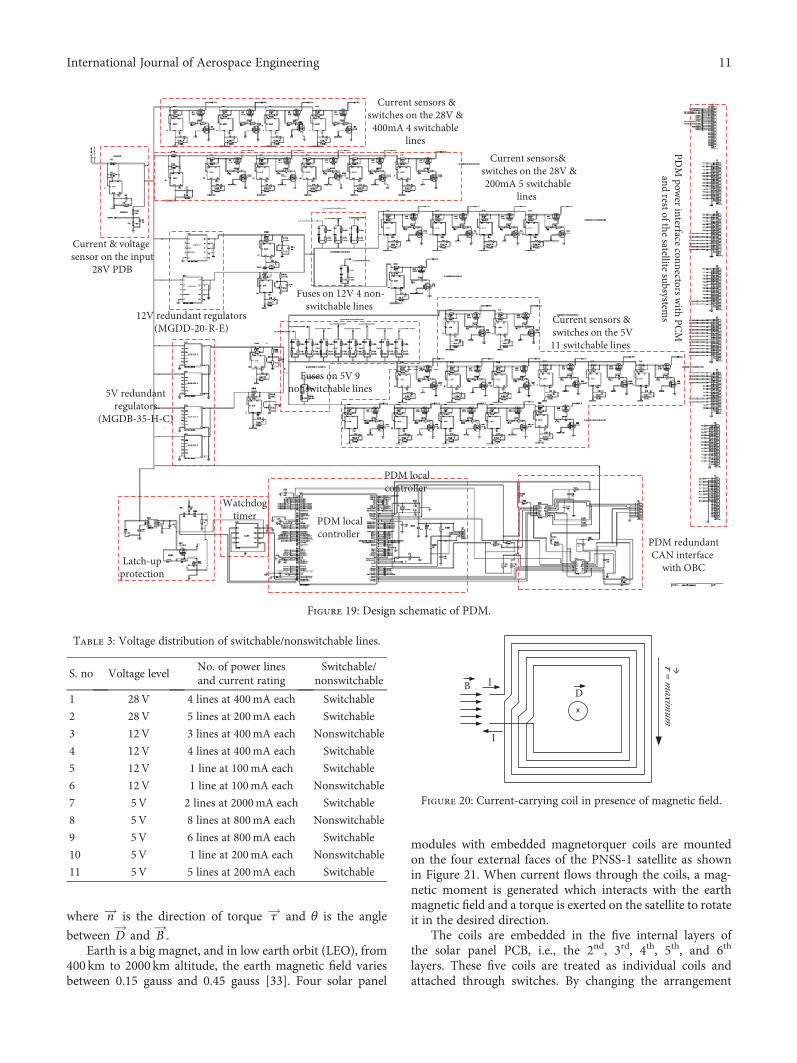
voltage, and temperature limitations. The PDM controllerfurther communicates with the OBC of the microsatellitethrough redundant CAN buses. The block diagram of thePDM is shown in Figure 18, and the design schematic isshown in Figure 19.
4.1. Power Regulators. The power regulators convert the PDBvoltage level to low voltage levels (i.e., 5V and 12V) used bydifferent subsystem components. For this purpose, the PDMunit requires two switching regulators. To meet the powerand redundancy requirement for 12V regulated output, thePDM has two redundant 12V regulators with part numberMGDD-20-R-E. For 5V, four regulators with part numberMGDB-35-H-C are connected in parallel to meet the powerand redundancy requirements.
4.2. Power Interface. The PDM receives unregulated powerthrough the PDB from the PCM and regulates it accordingto the requirement. For redundancy, the PDM receives 2 : 1power lines from the PCM at 28V± 6V. The PDM has a totalof 40 output lines of different voltage and current levels.Some of these lines are pair switchable and some are non-switchable as shown in Table 3.
All output distribution lines of the PDM are protectedagainst short circuit current and transient voltage spikes. Aprotection concept is implemented in the PDM to avoidfault and failure propagation between the loads. All PDMsubsystems are connected and intercommunicate with thePDM controller (PIC24HJ256GP10) for monitoring andcontrolling purposes.
4.3. Data Interface. The PDM has a dual redundant CANinterface with the OBC for all telemetries and all of its tele-commands. With the help of the CAN interface, the OBCreceives certain telemetries from the PDM in order to checkall the switchable distribution lines as well as to monitorthe health of the primary and secondary voltages. In orderto control the ON/OFF operation of switchable lines, thePDM has the capability of receiving telecommands throughthe CAN interface. Standard D-type connectors are usedfor CAN buses.
8070605040302010
00 0.5 1 1.5 2 2.5 3 3.5 4
Volta
ge (V
)
Time (ms)
Output from solar panelBuck converter output
Figure 14: Input and output voltage waveforms for 50V input.
86420
−2
−4
−6
−80 0.05 0.1 0.15 0.2 0.25 0.3 0.35 0.4 0.45 0.5
Curr
ent (
A)
Time (ms)
Output current of Buck converterBuck converter switching current
Figure 15: Input and output current waveforms for 50V input.
60
50
40
30
20
10
00 0.5 1 1.5 2 2.5 3 3.5 4
Volta
ge (V
)
Time (ms)
Output from solar panelBuck converter output
Figure 16: Input and output voltage waveforms for 41V input.
86420
−2
−4
−6
−80 0.05 0.1 0.15 0.2 0.25 0.3 0.35 0.4 0.45 0.5
Curr
ent (
A)
Time (ms)
Output current of Buck converterBuck converter switching current
Figure 17: Input and output current waveforms for 41V input.
9International Journal of Aerospace Engineering

5. Attitude Control System (ACS)
Due to dimension and weight constraints of small satellites,designers are focusing on the miniaturization of subsystemssuch as power, attitude determination and control, telecom-munication, and payload. In the PNSS-1 attitude controlsubsystem design, the major aim was to achieve a systemwith small dimensions and weight. The available optionsfor the attitude control were permanent magnets, reactionwheels, and magnetic rods [31, 32]. Permanent magnetsare cheaper, simpler, and lightweight, but they have inade-quate pointing accuracy. The other options were magneticrods and reaction wheels which have better pointing accu-racy, but the problem is their price, weight, and size whichmake them unsuitable for small satellites. To achieve thegoal of a miniaturized compatible system with PNSS-1, aninnovative concept of an embedded magnetorquer is intro-duced. The magnetorquer coil is copper traces embeddedinside the internal layers of the solar panel PCB. Solar panelPCB is an eight-layer PCB with copper traces in five inter-nal layers. These copper traces are just like the magnetor-quer rod producing a magnetic field when current flowsthrough it.
5.1. PNSS-1 Embedded Magnetorquer Coil. The magnetor-quer coil works on the motor action concept that when a cur-rent carrying the coil is placed in a magnetic field, a torque isexerted on the coil. The current-carrying coil generates amagnetic moment which interacts with the already existingmagnetic field and produces torque. According to Fleming’sleft-hand rule, the middle finger gives the direction of themagnetic moment, the index finger shows the direction ofthe existing magnetic field, and the thumb indicates thedirection of exerted torque. Let us suppose the current-carrying coil shown in Figure 20 with the magnetic moment(D) generated is toward the page and is given by
D =N ⋅ S ⋅ I, 3
where N is the number of turns of the coil, S is the area of thecoil, and I is the current flowing through the coil.
If the magnetic field ( B ) direction is toward the right sideof the paper, then the torque generated is toward the bottomof the paper and can be found by
τ = D × B =DB sin θ n , 4
Table 2: Simulation results of MPPT buck converter designed for PCM.
S. noInput voltage
(Vin)Output voltage
(Vo)Duty cycle
(D)Input current
(Iin)Output current
(Io)Input power
(Pin)Output power
(Po)Efficiency
(η)
1 80V 27.33V 0.35 0.981A 2.73A 78.28W 74.61W 95.30
2 70V 27.36V 0.40 1.11A 2.73A 77.50W 74.69W 96.37
3 61V 27.45V 0.46 1.28A 2.74A 77.87W 75.21W 96.58
4 50V 27.45V 0.56 1.56A 2.74A 77.79W 75.21W 96.68
5 41V 27.39V 0.68 1.89A 2.73A 77.28W 74.77W 96.75
Satellitesubsystems
5V/12Vload switch
12V outputload switch
5V outputload switch
3.3V outputload switch
PDB(28±6V)load switch
3.3Vregulator
5Vregulator
12Vregulator
3.3V inputload switch
5V inputload switch
12V input load switch
Latch-upprotection
PDUcontroller
CAN-1 CAN-2
Voltagesensor
Currentsensor
Currentsensor
Output ofPCU (PDB-1)
Output ofPCU (PDB-2)
(a)
Ground planes
0.4 mm
1.6 mm
Components
Layer-1
Layer-3Layer-4
Layer-2
1.66.46.69.0
9.15
8.3
(0,0)
90 mm
120
mm
3.2
3.2
10.8 Ø3.8
Ø3.8
Ø3.8
Ø3.8
PDB-1 from PCU
DB9 connector
1
Regulators,load switches,housekeeping
sensors(current,voltage &
temperature)
PCU controller,latch-up
protection and auxiliary components
DB9connector
2
DB9connector
3
DB9connector
4
DB9connector
5
DB9connector
6
CAN
/RS232Connector-2
CAN
/RS232Connector-1
PDB-2 fromPCU
(b)
Figure 18: (a) PDM block diagram and (b) PCB dimensions.
10 International Journal of Aerospace Engineering
where n is the direction of torque τ and θ is the angle
between D and B .Earth is a big magnet, and in low earth orbit (LEO), from
400 km to 2000 km altitude, the earth magnetic field variesbetween 0.15 gauss and 0.45 gauss [33]. Four solar panel
modules with embedded magnetorquer coils are mountedon the four external faces of the PNSS-1 satellite as shownin Figure 21. When current flows through the coils, a mag-netic moment is generated which interacts with the earthmagnetic field and a torque is exerted on the satellite to rotateit in the desired direction.
The coils are embedded in the five internal layers ofthe solar panel PCB, i.e., the 2nd, 3rd, 4th, 5th, and 6th
layers. These five coils are treated as individual coils andattached through switches. By changing the arrangement
Current & voltage sensor on the input
28V PDB
Current sensors &switches on the 28V & 400mA 4 switchable
lines Current sensors&
switches on the 28V &200mA 5 switchable
lines
Fuses on 12V 4 non-switchable lines
12V redundant regulators(MGDD-20-R-E)
5V redundantregulators
(MGDB-35-H-C)
Fuses on 5V 9 nonswitchable lines
Current sensors & switches on the 5V11 switchable lines
PDM localcontroller
PDM localcontroller
PDM redundantCAN interface
with OBCLatch-upprotection
Watchdogtimer
PDM
power interface connectors w
ith PCM
and rest of the satellite subsystems
Figure 19: Design schematic of PDM.
Table 3: Voltage distribution of switchable/nonswitchable lines.
S. no Voltage levelNo. of power linesand current rating
Switchable/nonswitchable
1 28V 4 lines at 400mA each Switchable
2 28V 5 lines at 200mA each Switchable
3 12V 3 lines at 400mA each Nonswitchable
4 12V 4 lines at 400mA each Switchable
5 12V 1 line at 100mA each Switchable
6 12V 1 line at 100mA each Nonswitchable
7 5V 2 lines at 2000mA each Switchable
8 5V 8 lines at 800mA each Nonswitchable
9 5V 6 lines at 800mA each Switchable
10 5V 1 line at 200mA each Nonswitchable
11 5V 5 lines at 200mA each Switchable
I
I
DB
→𝜏 = maxim
um
Figure 20: Current-carrying coil in presence of magnetic field.
11International Journal of Aerospace Engineering

of these switches, the five coils can be attached/detached indifferent configurations such as a single coil, five in series,and five coils in parallel. According to the satellite torquerequirements, the magnetorquer coil should be able to gener-ate a specific magnetic field. To generate the required mag-netic moment of PNSS-1, the magnetorquer coil composedof copper traces with 60 turns in each layer and a total of300 turns is embedded in five internal layers. Each coil tracehas 1.8mm width and 18μm thickness. Space between twoadjacent traces is 0.2mm.
Current, magnetic moment, and power dissipated areplotted against voltage in Figure 22, for four coils connectedin series and parallel. At a particular voltage, one can observeand compare all the other parameters.
6. Conclusion
The paper proposed a modular design for the EPS and ACSof a microsatellite. The complete EPS is divided into threesubmodules, i.e., the SPM, PCM, and PDM. Every modulehas data and power interfaces which are standardized with
specific number of input/output lines that meet the powerand data requirement of microsatellite subsystems. COTScomponents were used for the subsystem implementation.The COTS components were selected on the basis of smalldimension, minimum weight, and low power consumption.To avoid single component failure and increase the reliabil-ity, certain subsystems and components were made redun-dant in the design. To operate the solar panels at MPP andextract maximum power from them, a wide range highly effi-cient MPPT-based buck converter is designed and analyzed.Each solar panel has a separate MPPT unit with a 10 kHz fre-quency gap to avoid synchronization between them. To pro-tect the CMOS-based controllers from radiation, a latch-upprotection system is designed and simulated. Different sen-sors such as current, temperature, and voltage are mountedat different locations on the respective modules to monitorand ensure proper operation of these units. For miniaturiza-tion purposes, an embedded magnetorquer is designed forthe microsatellite which consumes reasonable power andgenerates the required magnetic moment. In the end, anEPS for the microsatellite is achieved which is fully modular,compact, redundant, and power efficient.
Data Availability
The data used to support the findings of this study areincluded within the article.
Conflicts of Interest
The authors announce that there is no conflict of interestconcerning the publication of this article.
References
[1] C. Passerone, M. Tranchero, S. Speretta, L. Reyneri, C. Sansoe,and D. Del Corso, “Design solutions for a university nano-sat-ellite,” in 2008 IEEE Aerospace Conference, pp. 1–13, Big Sky,MT, USA, March 2008.
[2] J. C. de los Rios, D. Roascio, L. Reyneri et al., “ARAMIS: afine-grained modular architecture for reconfigurable spacemissions,” in 1st Conference on University Satellite Missions,Rome, January 2011.
[3] A. Ali, L. M. Reyneri, and M. Rizwan Mughal, InnovativeElectric Power Supply System for Nano-Satellites, 64THIAC, Beijing China, 2013.
1.6
mm
0.2 mm
Magnetorquer coil traces
18 𝜇mLayer-1Layer-2Layer-3
Layer-8
0.2 mm
Ground plane
1.8 mm
Solar cells
450 mm 450 mm
Figure 21: Solar panel module (PNSS-1) cross-sectional view with embedded magnetorquer.
0 2 4 6 8 10Voltage (V)
0.1×
I(A
), Pd
(W),
D(A
m2)
12 14 16 18
4.5
4
3.5
3
2.5
2
1.5
1
0.5
0
Current I in seriesPower dissipated Pd in seriesMagnetic moment D in series
3× magnetic moment D in parallel
6× current I in parallel10× power dissipated Pd in parallel
Figure 22: Voltage versus current, magnetic moment, and powerdissipated for four-coil combination (series/parallel).
12 International Journal of Aerospace Engineering

[4] D. Del Corso, C. Passerone, L. M. Reyneri et al., “Architectureof a small low-cost satellite,” in 10th Euromicro Conference onDigital System Design Architectures, Methods and Tools (DSD2007), Lubeck, Germany, August 2007.
[5] D. De Bruyn, “Power distribution and conditioning for a smallstudent satellite, design of the NUTS backplane & EPS mod-ule,” in Master of Science in Engineering Cybernetics, Norwe-gian University of Science and Technology (NTNU), 2011.
[6] “Satellite mass categories,” http://www.daviddarling.info/encyclopedia/S/satellite_mass_categories.html.
[7] S. Dahbi, A. Aziz, S. Zouggar et al., “Power budget analysis fora LEO polar orbiting nano-satellite,” in 2017 InternationalConference on Advanced Technologies for Signal and ImageProcessing (ATSIP), pp. 1–6, Fez, Morocco, May 2017.
[8] “Universities in space: seriously higher education,” http://spaceflight.com/universities-in-space-seriously-higher-education/.
[9] “World’s largest database of nanosatellites, over 2150 nanosatsand Cube Sats,” https://www.nanosats.eu/.
[10] “Introduction to PNSS-P (1),” January 2014, http://suparco.gov.pk/pages/intro.asp,suparco.gov.pk/pages/presentations-pdf/day-1/session-1/12B-III/4.pdf.
[11] C.-S. Sun and J.-C. Juang, “Design and implementation ofa microsatellite electric power subsystem,” Journal of Aero-nautics, Astronautics and Aviation Series A, vol. 44, no. 2,pp. 67–74, 2012.
[12] S. Greenland, P. Mendham, M. Macdonald, C. McInnes, andC. Clark, “Implementation of a product-centric space systemapproach to nanosatellite systems design and deployment,”in The 4S Symposium 2016, Valletta, Malta, May-June 2016.
[13] M. R. Mughal, J. C. De Los Rios, L. M. Reyneri, and A. Ali,“Scalable plug and play tiles for modular nano satellites,” in63rd International Astronautical Congress, Naples, Italy, Octo-ber 2012.
[14] J. Esper, “Modular, adaptive, reconfigurable systems: technol-ogy for sustainable, reliable, effective, and affordable spaceexploration,” AIP Conference Proceedings, vol. 746, pp. 1033–1043, 2005.
[15] K. B. Clark and C. Y. Baldwin, Design Rules. Vol. 1: The Powerof Modularity, MIT Press, Cambridge, Massachusetts, 2000.
[16] P. M. Wegner, P. Blower, and J. Wilkenfeld, “Standard buses,modular buses, and plug-and-play buses; what is the differenceand why does it matter?,” Report No. A553345, 2008.
[17] J. S. O. Alvarado, J. S. R. Mora, and L. E. A. Pico, “Designs andimplementations for CubeSat Colombia 1 satellite power mod-ule,” International Journal of Applied Engineering Research,vol. 12, no. 18, pp. 7360–7371, 2017.
[18] B. Burger and R. Rüther, “Inverter sizing of grid-connectedphotovoltaic systems in the light of local solar resource distri-bution characteristics and temperature,” Solar Energy, vol. 80,no. 1, pp. 32–45, 2006.
[19] M. Green, General Temperature Dependence of Solar CellPerformance and Implications for Device Modeling, JohnWiley & Sons, Ltd., 2003.
[20] W. J. Larson, Space Mission Analysis and Design, ThirdEdition, p. 217, 1999.
[21] P. C. M. De Carvalho, R. S. T. Pontes, D. S. Oliveira, D. B.Riffel, R. G. V. de Oliveira, and S. B. Mesquita, “Controlmethod of a photovoltaic powered reverse osmosis plantwithout batteries based on maximum power point tracking,”in 2004 IEEE/PES Transmision and Distribution Conference
and Exposition: Latin America (IEEE Cat. No. 04EX956),pp. 137–142, Sao Paulo, Brazil, November 2004.
[22] M. Park and I. K. Yu, “A study on optimal voltage for MPPTobtained by surface temperature of solar cell,” in 30th AnnualConference of IEEE Industrial Electronics Society, 2004. IECON2004, pp. 2040–2045, Busan, South Korea, November 2004.
[23] T. Takashima, T. Tanaka, M. Amano, and Y. Ando, “Maximumoutput control of photovoltaic (PV) array,” in Collection ofTechnical Papers. 35th Intersociety Energy Conversion Engineer-ing Conference and Exhibit (IECEC) (Cat. No.00CH37022),pp. 380–383, Las Vegas, NV, USA, July 2000.
[24] N. Femia, D. Granozio, G. Petrone, G. Spagnuolo, andM. Vitelli, “Optimized one-cycle control in photovoltaic gridconnected applications,” IEEE Transactions on Aerospaceand Electronic Systems, vol. 42, no. 3, pp. 954–972, 2006.
[25] W. Wu, N. Pongratananukul, W. Qiu, K. Rustom, T. Kasparis,and I. Batarseh, “DSP-based multiple peak power tracking forexpandable power system,” in Eighteenth Annual IEEE AppliedPower Electronics Conference and Exposition, 2003. APEC '03,pp. 525–530, Miami Beach, FL, USA, February 2003.
[26] C. Hua and C. Shen, “Comparative study of peak power track-ing techniques for solar storage system,” in APEC '98 Thir-teenth Annual Applied Power Electronics Conference andExposition, pp. 679–685, Anaheim, CA, USA, February 1998.
[27] D. P. Hohm andM. E. Ropp, “Comparative study of maximumpower point tracking algorithms using an experimental, pro-grammable, maximum power point tracking test bed,” Confer-ence Record of the Twenty-Eighth IEEE Photovoltaic SpecialistsConference - 2000 (Cat. No.00CH37036), 1699–1702, Anchor-age, AK, USA, September 2000, 1699–1702.
[28] A. Dolara, R. Faranda, and S. Leva, “Energy comparison ofseven MPPT techniques for PV systems,” Journal of Electro-magnetic Analysis and Applications, vol. 1, no. 3, pp. 152–162, 2009.
[29] P. Ehrenfreund, B. H. Foing, and F. Salama, “Organics inspace: results from space exposure platforms and nanosatel-lites,” in IAU General Assembly, Meeting #29, id. 2257551,American Astronomical Society, 2015.
[30] D. W. Hart, Power Electronics, mcgraw-Hill, New York, NY,USA, 2011, Print.
[31] N. Shams, F. Tanveer, and S. Ahmad, “Design and develop-ment of attitude control system (ACS) using COTS basedcomponents for small satellites,” in 2008 2nd InternationalConference on Advances in Space Technologies, pp. 6–11,Islamabad, Pakistan, November 2008.
[32] V. Francois-Lavet, Study of Passive and Active Attitude ControlSystems for the OUFTI Nanosatellites, University of Liege Fac-ulty of Applied Sciences, 2009–2010.
[33] “SPENVIS: The Space Environment Information System,”http://www.spenvis.oma.be.
13International Journal of Aerospace Engineering

International Journal of
AerospaceEngineeringHindawiwww.hindawi.com Volume 2018
RoboticsJournal of
Hindawiwww.hindawi.com Volume 2018
Hindawiwww.hindawi.com Volume 2018
Active and Passive Electronic Components
VLSI Design
Hindawiwww.hindawi.com Volume 2018
Hindawiwww.hindawi.com Volume 2018
Shock and Vibration
Hindawiwww.hindawi.com Volume 2018
Civil EngineeringAdvances in
Acoustics and VibrationAdvances in
Hindawiwww.hindawi.com Volume 2018
Hindawiwww.hindawi.com Volume 2018
Electrical and Computer Engineering
Journal of
Advances inOptoElectronics
Hindawiwww.hindawi.com
Volume 2018
Hindawi Publishing Corporation http://www.hindawi.com Volume 2013Hindawiwww.hindawi.com
The Scientific World Journal
Volume 2018
Control Scienceand Engineering
Journal of
Hindawiwww.hindawi.com Volume 2018
Hindawiwww.hindawi.com
Journal ofEngineeringVolume 2018
SensorsJournal of
Hindawiwww.hindawi.com Volume 2018
International Journal of
RotatingMachinery
Hindawiwww.hindawi.com Volume 2018
Modelling &Simulationin EngineeringHindawiwww.hindawi.com Volume 2018
Hindawiwww.hindawi.com Volume 2018
Chemical EngineeringInternational Journal of Antennas and
Propagation
International Journal of
Hindawiwww.hindawi.com Volume 2018
Hindawiwww.hindawi.com Volume 2018
Navigation and Observation
International Journal of
Hindawi
www.hindawi.com Volume 2018
Advances in
Multimedia
Submit your manuscripts atwww.hindawi.com