design of photonic crystal waveguides for evanescent...
TRANSCRIPT
2274 J. Opt. Soc. Am. B/Vol. 20, No. 11 /November 2003 Barclay et al.
Design of photonic crystal waveguides forevanescent coupling to optical fiber
tapers and integration with high-Q cavities
Paul E. Barclay, Kartik Srinivasan, and Oskar Painter
Department of Applied Physics, California Institute of Technology, Pasadena, California 91125
Received November 15, 2002; revised manuscript received July 2, 2003; accepted July 31, 2003
We describe a novel scheme based on evanescent guided-wave coupling for optically interfacing between con-ventional fiber-optic and planar photonic crystal devices such as waveguides and resonant cavities. By con-sidering the band structure of bulk photonic crystal slabs, we analyze the k space properties of a linear defectwaveguide and establish a set of design rules to ensure efficient evanescent coupling with optical fiber tapers.These rules are used to design a waveguide in a square-lattice photonic crystal. The coupling efficiency iscalculated with a coupled-mode theory incorporating the finite-difference time-domain-calculated uncoupledmodes of the fiber taper and photonic crystal waveguide. On the basis of this coupled-mode theory, 95% powertransfer from the fiber taper to the photonic crystal waveguide is possible over a coupling length of 80 latticeperiods and with a bandwidth of 1.5% of the center wavelength. The integration of this waveguide with aphotonic crystal defect resonant cavity is also presented, thus showing the usefulness of the combined fibertaper and photonic crystal waveguide system for efficient, optical fiber-based probing of optical elements basedon planar photonic crystal technologies. © 2003 Optical Society of America
OCIS codes: 130.2790, 230.7370.
1. INTRODUCTIONSince the first proposal of photonic bandgap (PBG) mate-rials and their use for spontaneous emission control,1
high-index-contrast periodic dielectric structures, photo-nic crystals (PCs), have promised novel control of thepropagation and dispersion of light. Two-dimensional(2-D) PC slab waveguide structures2–5 offer a practical ge-ometry for the implementation of PC devices by means ofconventional planar lithography and semiconductor pro-cessing techniques. Planar PC technologies in a varietyof material systems, such as silicon-on-insulator, GaAs,and InP, have been used to realize such devices aswaveguides,6,7 lasers,8 coupled-resonator waveguidesystems,9–11 and add–drop filters,12,13 to name just a few.Resonant cavities formed in planar PC slabs, with modevolumes approaching a cubic half-wavelength, have alsoattracted some interest for use in cavity QEDexperiments14–16 and in single-photon sources.17–19 Theutility of these types of device relies heavily on one’s abil-ity to efficiently couple light into and out of the planar PC.
Because of the large refractive index of current planarPC-based materials (required for high-index-contraststructures), the spatial mismatch between optical fibermodes, or diffraction-limited free-space beams, andsingle-mode PC devices is severe. Recent progress in thedesign of adiabatic and tapered transitions20–22 betweenstandard index-guided waveguides and PC waveguideshas improved the theoretical efficiency of end-fire cou-pling schemes. However, because many of the applica-tions and advantages of planar PCs are seen in the inte-gration and miniaturization of components, the longadiabatic transitions from high-index index-guidedwaveguides with relatively small mode sizes to weakly
0740-3224/2003/112274-11$15.00 ©
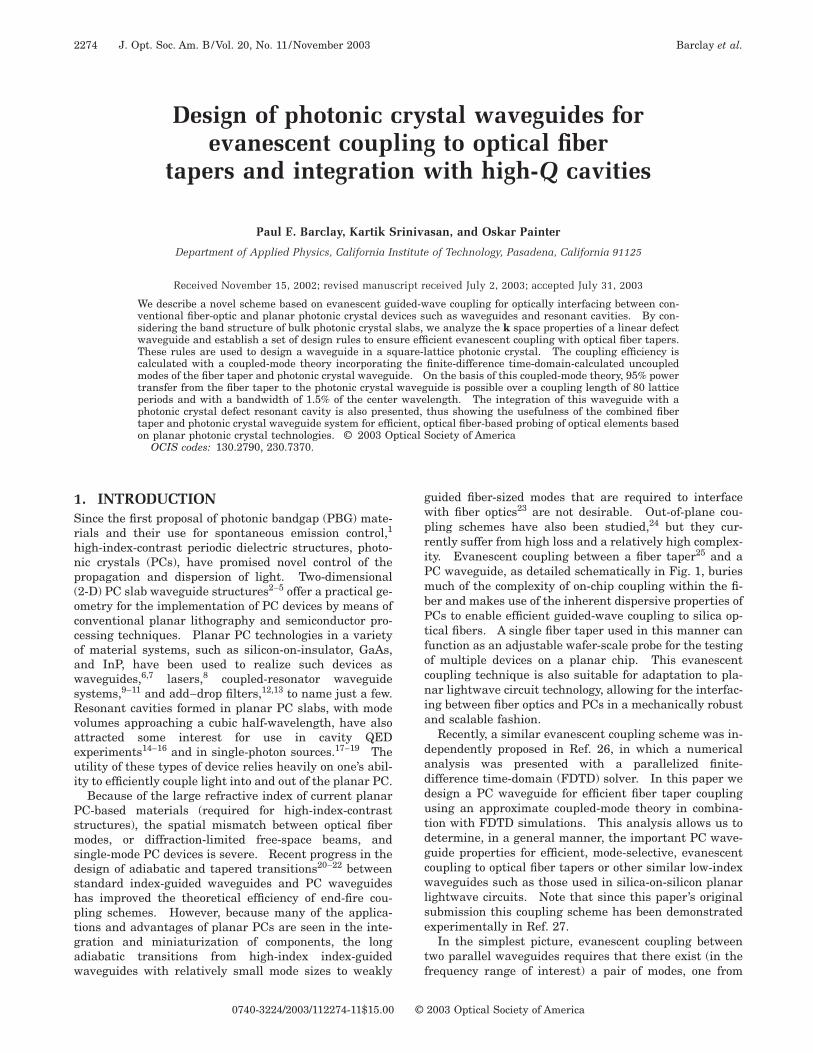
guided fiber-sized modes that are required to interfacewith fiber optics23 are not desirable. Out-of-plane cou-pling schemes have also been studied,24 but they cur-rently suffer from high loss and a relatively high complex-ity. Evanescent coupling between a fiber taper25 and aPC waveguide, as detailed schematically in Fig. 1, buriesmuch of the complexity of on-chip coupling within the fi-ber and makes use of the inherent dispersive properties ofPCs to enable efficient guided-wave coupling to silica op-tical fibers. A single fiber taper used in this manner canfunction as an adjustable wafer-scale probe for the testingof multiple devices on a planar chip. This evanescentcoupling technique is also suitable for adaptation to pla-nar lightwave circuit technology, allowing for the interfac-ing between fiber optics and PCs in a mechanically robustand scalable fashion.
Recently, a similar evanescent coupling scheme was in-dependently proposed in Ref. 26, in which a numericalanalysis was presented with a parallelized finite-difference time-domain (FDTD) solver. In this paper wedesign a PC waveguide for efficient fiber taper couplingusing an approximate coupled-mode theory in combina-tion with FDTD simulations. This analysis allows us todetermine, in a general manner, the important PC wave-guide properties for efficient, mode-selective, evanescentcoupling to optical fiber tapers or other similar low-indexwaveguides such as those used in silica-on-silicon planarlightwave circuits. Note that since this paper’s originalsubmission this coupling scheme has been demonstratedexperimentally in Ref. 27.
In the simplest picture, evanescent coupling betweentwo parallel waveguides requires that there exist (in thefrequency range of interest) a pair of modes, one from
2003 Optical Society of America
Barclay et al. Vol. 20, No. 11 /November 2003 /J. Opt. Soc. Am. B 2275
each waveguide, that share a common momentum compo-nent down the waveguide (phase matching) and for whichtheir transverse profiles and electric field polarizationsare similar. A weak spatial overlap of the evanescenttails of each mode can then result in significant powertransfer between the waveguides. Full power transferrequires that, in addition, no other radiation or guidedmodes of either waveguide participate in the coupling, ei-ther due to a large phase mismatch or weak transverseoverlap. Fiber taper coupling has been shown to be ex-tremely valuable in this regard (compared with simpleprism coupling that involves a continuum of modes), pro-viding near-perfect single-mode to single-mode couplingbetween tapers and dielectric microsphere28 and toroid29
resonators for ultrasensitive measurement of high-Qwhispering-gallery modes. In a similar manner fibertaper probes can be used to couple to 2-D PC membranewaveguides thanks to their undercut air-bridge structurethat suppresses radiation from the fiber into the sub-strate and their zone-folded dispersion that enables phasematching between the dissimilar fiber and the PC modes.Thus, by designing a PC waveguide whose defect modehas a transverse field profile that sufficiently overlaps thefiber taper’s fundamental mode field profile, we canachieve efficient power transfer between the waveguides.Furthermore, the flexibility in lattice engineering af-forded by PCs allows this waveguide to simultaneously bedesigned to couple efficiently to PC defect cavities, provid-ing a fiber–PC waveguide–PC cavity optical probe. Inthis paper we discuss the design of a PC waveguide thatsatisfies the requirements outlined above. In Section 2 asimple coupled-mode theory that models coupling be-tween a fiber taper and a PC is presented, and the desiredwaveguide properties are illuminated mathematicallyand discussed in more detail. In Section 3 a generalk space analysis of bulk PC band structures is used to de-
Fig. 1. (a) Schematic of the coupling scheme showing the four-mode basis used in the coupled-mode theory. (b) Coupling ge-ometry. In the case considered here the coupling is contradirec-tional. WG, waveguide. (c) Grading of the hole radius used toform the waveguide and a top view of the graded-defectcompressed-lattice (Lx /Lz 5 0.8) waveguide unit cell.
termine which types of defect mode have the desired prop-erties. The results from these sections are then appliedto the design and analysis of a PC waveguide in a squarelattice in Section 4 and are further illustrated with FDTDsupermode calculations in Section 5. Finally in Section 6we show how this waveguide can be used to probe high-QPC resonant cavities.
2. COUPLED-MODE THEORYIt has long been realized that modes in translationally in-variant waveguides with differing dielectric constants canbe phase matched with the aid of a grating, so it is notsurprising that the intrinsic discrete translational sym-metry of PC waveguides and the resulting zone-foldeddispersion of their modes allows PCs to be phase matchedwith a large class of dissimilar waveguides including ta-pered fibers. Grating-mediated phase-matching schemeshave been studied extensively beginning with the re-search of microwave traveling-wave tubes30 and more re-cently of optical devices such as filters, directional cou-plers, and distributed feedback lasers (Ref. 31 andreferences therein). However, because the dielectric con-trast of a PC grating is large, fiber–PC coupling differsfrom that of a traditional (weak) grating-assisted coupler;rather than analyze coupling between plane waves of theuntextured waveguides, the Bloch eigenmodes of the PCmust be considered. Although rigorous coupled-modetheories for Bloch modes have been developed in the con-text of nonlinear perturbations to Bragg fibers,32 photoniccrystals,33 and coupled-resonator optical waveguides,34
none of these formalisms consider coupling between par-allel waveguides. To evaluate the properties of evanes-cent coupling between a fiber and a PC defect waveguide,we present a coupled-mode theory that allows us to ap-proximately predict the power transfer between the PCBloch modes and the fiber plane-wave modes as a func-tion of propagation distance, transverse couplingstrength, and phase mismatch.
The physical system that we model is specified by thedielectric constants of the interacting waveguides em(r),each of which individually supports a set of modes En
m(r),where m labels the waveguides and n labels the eigen-modes of each waveguide. For exp(2ivt) time depen-dence, Maxwell’s equations require that each of thesemodes satisfies the eigenvalue equation
¹ 3 ¹ 3 Enm~r! 5 v2em~r!En
m~r!, (1)
where v 5 v/c is the free-space wave number.The fundamental approximation of waveguide coupled-
mode theories is that, after some propagation distance,the field of the composite system represented by e(r)5 e1 ù e2 ... ù en can be approximated by some linearcombination of the modes of the constituent systems rep-resented by em(r):
E~r! 5 (mn
Cnm~z !En
m~r!, (2)
where we assumed that the modes are propagating in the6z direction, or more precisely that the power flux of theindividual modes in the z direction is constant. When we
2276 J. Opt. Soc. Am. B/Vol. 20, No. 11 /November 2003 Barclay et al.
consider continuums of delocalized modes, an integral re-places the discrete sum. If em(r) is periodic in z so thatem(x, y, z 1 Lz) 5 em(x, y, z), by Bloch’s theorem35 theeigenmodes have z dependence of the form En
m(x, y,z 1 Lz) 5 exp(ibnLz)En
m(x, y, z) and Eq. (1) becomes
Hbnebn
m~r! 5 v2em~r!ebn
m~r!, (3)
where
Hbn5 @2bn
2z 3 z 1 ibn~ z 3 ¹ 1 ¹ 3 z ! 1 ¹ 3 ¹# 3 ,(4)
ebn
m(x, y, z 1 Lz) 5 ebn
m(x, y, z), and 2p/Lz , bn
< p/Lz (i.e., bn is restricted to the first Brillouin zone) sothat the eigenmodes are not overcounted. Equation (3) isoften solved as an eigenvalue problem for vn parameter-ized by the wave number b, giving a dispersion relationvn 5 vn(b). In linear media, only modes degenerate inv have nonzero time-averaged coupling over typical labo-ratory time scales, and it is convenient to label the modesat fixed v by their wave number bn(v). Both conven-tions are equivalent and interchangeable. Typically (asdiscussed below) for weak coupling, only modes nearlyresonant in b (modulo a reciprocal lattice vector 2p/Lz) tothe exciting field need to be included in Eq. (2); this is thebasic assumption of the coupled-mode theory. For weakcoupling this assumption that only nearly resonant modesinteract is reasonable; however, the question of complete-ness is less clear. In general Eq. (2) cannot satisfy Max-well’s equations because the eigenmodes of waveguide m1do not satisfy the boundary conditions of waveguide m2and vice versa. This issue was debated vigorously in thelate 1980s but was not resolved, it is well summarized inRef. 36. In Ref. 37 Haus and Snyder showed that insome cases the ansatz Eq. (2) can be improved when themodes used in the expansion are modified so that theysatisfy the boundary conditions of the composite system.This improvement is nontrivial in the case of a PC slab,however, and is not used here. This deficiency is mini-mized for TE-like modes but exists nonetheless if thewaveguides lack translational invariance or planar geom-etry as is the case in PC waveguides and fiber tapers, re-spectively. Despite this limitation we proceed under theassumption that, in the limit of weak coupling, the result-ing model is a useful design tool that correctly describesthe dependence of the coupling on the physical param-eters but whose absolute results may deviate from the ex-act values.
To formulate coupled-mode equations we assume thatansatz Eq. (2) is a solution to Maxwell’s equations for thehybrid system and we employ the Lorentz reciprocityrelationship38 that must hold for any two solutions toMaxwell’s equations in nonmagnetic materials:
]
]zE
z~E1 3 H2* 1 E2* 3 H1! • zdxdy
5 ivEzE1–E2* ~e1 2 e2* !dxdy, (5)
where (E, H)1,2 satisfy Maxwell’s equations for e1,2 . Set-ting
E1 5 (j
Cj~z !Ej~r!,
E2 5 Ei , (6)
and correspondingly
e1 5 e,
e2 5 e i , (7)
where the single index i 5 (m i , n i), labeling both thewaveguide and the mode is adopted for clarity, and sub-stituting Eqs. (6) and (7) into Eq. (5) we obtain the follow-ing power-conserving coupled-mode equations:
Pij
dCj
dz5 ivKijCj , (8)
where
Pij~z ! 5 Ez~Ei* 3Hj 1 Ej3Hi* ! • zdxdy, (9)
Kij~z ! 5 EzEi* –Ej~e 2 e j!dxdy, (10)
and it was assumed that all dielectric constants are real.Equation (8) is similar to the coupled-mode equationsgiven in Ref. 39, with the only differences arising from thefact that no specific form of z dependence of the eigen-modes was assumed. When the mode amplitudes arefixed at some z 5 z0 , Eq. (8) can easily be solved numeri-cally, giving a transfer matrix that maps the amplitudesat z0 to z0 1 L. To correctly model an experimentalsetup, the amplitude of the modes propagating in the 1zdirection should be fixed at z0 , and the amplitude of themodes propagating in the 2z direction should be fixed atz0 1 L. Equation (8) can be solved with these mixedboundary conditions by first calculating the transfer ma-trix [which maps Ci
6(z0) → Ci6(z0 1 L) where the su-
perscript represents the propagating direction of mode j]and then transforming it to the appropriate scatteringmatrix [which maps Ci
1(z0) → Ci1(z0 1 L) and Ci
2(z01 L) → Ci
2(z0)]. Alternately, we can solve Eq. (8) di-rectly using a boundary-value problem algorithm.
From Eq. (5) the diagonal terms Pii of the power matrixare constant and are typically normalized to plus or mi-nus unity depending on the sign of the group velocity ofmode i. In addition, it can be shown that Bloch modesof the same waveguide are power orthogonal so thatPij 5 0 if e i 5 e j and Ei Þ Ej . However, modes fromneighboring waveguides are not power orthogonal, result-ing in nonzero off-diagonal z-dependent components in Pijthat must be retained for Eq. (8) to be power conserving.In the fiber–PC system, the z dependence of the PC fieldsis the product of a plane-wave part and a periodic partwhereas fiber fields have a plane-wave-like z dependence.Expanding the periodic part of the PC field as well the PCdielectric constant in a Fourier series, the z dependence ofPij and Kij can be written in terms of superpositions ofexp@i(bi 2 bj 2 2pm/Lz)z# where m is an integer. Forweak coupling (dCj /dz ! 1/l), only the slowly varyingcomponent (compared with l) of Kij significantly couplesthe amplitude coefficients Ci and Cj over laboratory
Barclay et al. Vol. 20, No. 11 /November 2003 /J. Opt. Soc. Am. B 2277
length scales of interest. This reasoning is analogous to(for example) that used in the time-domain rotating-waveapproximation in quantum mechanics and is often used toderive approximate analytic solutions to coupled-modeequations describing two-mode electromagnetic systemsin the presence of weak gratings.40 Because of the strongdielectric contrast of the PC, the problem here is morecomplex; however, the fundamental results from thesimple cases hold: To observe significant power exchangebetween modes, their wave numbers b must differ by ap-proximately a reciprocal lattice vector 2pm/Lz . Also,the larger the phase-matched driving terms, the strongerthe coupling. The mixing of the Fourier components ofthe PC Bloch mode and the dielectric constant is the mostsignificant effect captured by this coupled-mode theorycompared with standard weak grating theories. Physi-cally this allows coupling between PC and fiber modesthat is mediated either directly by a Fourier coefficient ofthe PC Bloch mode (the dominant effect here) or indi-rectly by the PC dielectric acting like a grating (a higher-order effect). Optimizing the magnitude of these coeffi-cients and, as a result, the coupling from the fiber mode tothe desired PC waveguide mode is discussed in Section 3.
3. k SPACE DESIGNPC defect waveguides are formed when a line of defects isintroduced into an otherwise two- or three-dimensionallyperiodic PC. Here we consider pseudo-2-D membranestructures whose typical geometry is shown in Fig. 1. Inabsence of the defects, the eigenmodes of the bulk 2-Dslab are Bloch modes whose in-plane wave number k is agood mode label and that are bound to the slab if v(k) isbelow the cladding and substrate light lines, i.e., v(k), ck/nc,s where ns and nc are the indices of refraction ofthe substrate and cladding, respectively (we do not con-sider bound modes that exist at special points in v–kspace above the light line, as shown in Ref. 41). The air-bridge membrane structures considered here have nc5 ns 5 1, maximizing the area in v–k space wherebound modes exist and also ensuring that the boundmodes of a fiber taper (nf ' 1.45) do not leak into the PCsubstrate.
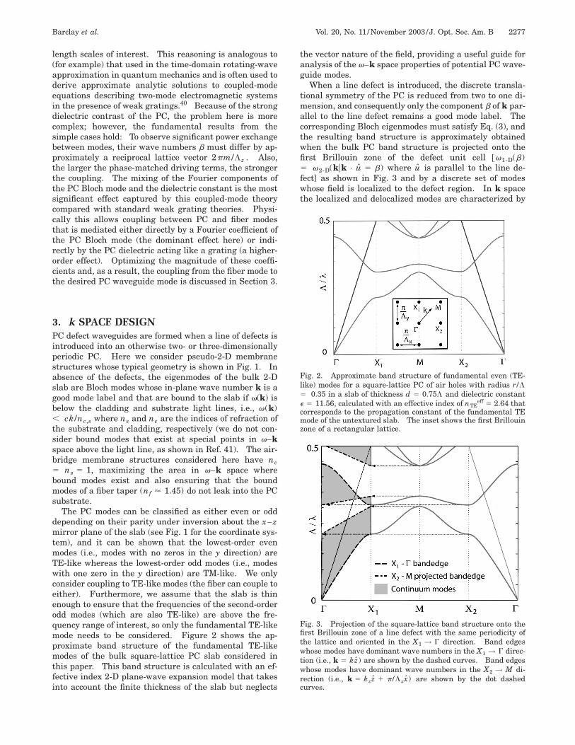
The PC modes can be classified as either even or odddepending on their parity under inversion about the x –zmirror plane of the slab (see Fig. 1 for the coordinate sys-tem), and it can be shown that the lowest-order evenmodes (i.e., modes with no zeros in the y direction) areTE-like whereas the lowest-order odd modes (i.e., modeswith one zero in the y direction) are TM-like. We onlyconsider coupling to TE-like modes (the fiber can couple toeither). Furthermore, we assume that the slab is thinenough to ensure that the frequencies of the second-orderodd modes (which are also TE-like) are above the fre-quency range of interest, so only the fundamental TE-likemode needs to be considered. Figure 2 shows the ap-proximate band structure of the fundamental TE-likemodes of the bulk square-lattice PC slab considered inthis paper. This band structure is calculated with an ef-fective index 2-D plane-wave expansion model that takesinto account the finite thickness of the slab but neglects
the vector nature of the field, providing a useful guide foranalysis of the v–k space properties of potential PC wave-guide modes.
When a line defect is introduced, the discrete transla-tional symmetry of the PC is reduced from two to one di-mension, and consequently only the component b of k par-allel to the line defect remains a good mode label. Thecorresponding Bloch eigenmodes must satisfy Eq. (3), andthe resulting band structure is approximately obtainedwhen the bulk PC band structure is projected onto thefirst Brillouin zone of the defect unit cell @v1-D(b)5 v2-D(kuk • u 5 b) where u is parallel to the line de-fect] as shown in Fig. 3 and by a discrete set of modeswhose field is localized to the defect region. In k spacethe localized and delocalized modes are characterized by
Fig. 2. Approximate band structure of fundamental even (TE-like) modes for a square-lattice PC of air holes with radius r/L5 0.35 in a slab of thickness d 5 0.75L and dielectric constante 5 11.56, calculated with an effective index of nTE
eff 5 2.64 thatcorresponds to the propagation constant of the fundamental TEmode of the untextured slab. The inset shows the first Brillouinzone of a rectangular lattice.
Fig. 3. Projection of the square-lattice band structure onto thefirst Brillouin zone of a line defect with the same periodicity ofthe lattice and oriented in the X1 → G direction. Band edgeswhose modes have dominant wave numbers in the X1 → G direc-tion (i.e., k 5 kz) are shown by the dashed curves. Band edgeswhose modes have dominant wave numbers in the X2 → M di-rection (i.e., k 5 kzz 1 p/Lxx) are shown by the dot dashedcurves.
2278 J. Opt. Soc. Am. B/Vol. 20, No. 11 /November 2003 Barclay et al.
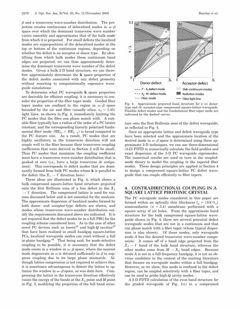
b and a transverse wave-number distribution. The pro-jection creates continuums of delocalized modes in v–bspace over which the dominant transverse wave numbervaries smoothly and approximates that of the bulk modefrom which it is projected. For small defects the localizedmodes are superpositions of the delocalized modes at thetop or bottom of the continuum regions, depending onwhether the defect is an acceptor or donor type. By iden-tifying from which bulk modes these continuum bandedges are projected, we can thus approximately deter-mine the dominant transverse wave number of the defectmodes. Given a bulk 2-D band structure, we can there-fore approximately determine the k space properties ofthe defect modes associated with any defect geometrywithout resorting to computationally expensive wave-guide simulations.
To determine what PC waveguide k space propertiesare desirable for efficient coupling, it is necessary to con-sider the properties of the fiber taper mode. Guided fibertaper modes are confined to the region in v–b spacebounded by the air and fiber (usually silica, nf ' 1.45)light lines, as shown in Fig. 4, immediately limiting thePC modes that the fiber can phase match with. A suit-able fiber typically has a radius of the order of a PC latticeconstant, and the corresponding linearly polarized funda-mental fiber mode (HE11 6 HE121) is broad compared tothe PC feature size. As a result, PC modes that arehighly oscillatory in the transverse direction will notcouple well to the fiber because their transverse couplingcoefficients that were derived in Section 2 will be small.Thus PC modes that maximize the coupling coefficientmust have a transverse wave-number distribution that ispeaked at zero (i.e., have a large transverse dc compo-nent). This corresponds to defect modes that are domi-nantly formed from bulk PC modes whose k is parallel tothe defect (the X1 → G direction here).
These ideas are illustrated in Fig. 4, which shows abulk compressed square-lattice band structure projectedonto the first Brillouin zone of a line defect in the X1→ G direction. The compressed lattice is used for rea-
sons discussed below and is not essential for the analysis.The approximate dispersion of localized modes formed byboth donor- and acceptor-type defects are shown, andmodes whose transverse wave-number distribution sat-isfy the requirements discussed above are indicated. It isnot required that the defect modes be in a full PBG for thecoupling scheme considered here. As in the case of othernovel PC devices such as lasers42 and high-Q cavities43
that have been realized in small bandgap square-latticePCs, localized waveguide modes can exist without a fullin-plane bandgap.44 That being said, for mode-selectivecoupling to be possible, it is necessary that the defectmode exists in a window in v–b space, where the nearestmode degenerate in v is detuned sufficiently in b to sup-press coupling due to its large phase mismatch. Al-though lattice compression is not required to achieve this,it is sometimes advantageous to distort the lattice to op-timize the window in v–b space, as was done here. Com-pressing the lattice in the transverse direction effectivelyraises the energy of the bands at the X2 point and M pointin Fig. 3, modifying the projection of the full band struc-
ture onto the first Brillouin zone of the defect waveguide,as reflected in Fig. 4.
Once an appropriate lattice and defect waveguide typehave been selected and the approximate location of thedesired mode in v–b space is determined using these ap-proximate 2-D techniques, we can use three-dimensional(3-D) FDTD to numerically calculate the field profiles andexact dispersion of the 3-D PC waveguide eigenmodes.The numerical results are used in turn in the coupled-mode theory to model the coupling to the tapered fibermodes. These design principles are applied in Section 4to design a compressed square-lattice PC defect wave-guide that can couple efficiently to fiber tapers.
4. CONTRADIRECTIONAL COUPLING IN ASQUARE LATTICE PHOTONIC CRYSTALThe PC waveguide modes considered in this paper areformed within an optically thin [thickness tg 5 (3/4)Lx]semiconductor (n 5 3.4) membrane perforated with asquare array of air holes. From the approximate bandstructure for the bulk compressed square-lattice wave-guide shown in Fig. 4, there are several potential defectwaveguide modes that are not in a continuum and thatcan phase match with a fiber taper (whose typical disper-sion is also shown). Of these modes, only waveguidemode A has the desired transverse wave-number compo-nents: It comes off of a band edge projected from theX1 → G band of the bulk band structure, whereas theother modes come from M → X2 band edges. Becausemode A is not in a full-frequency bandgap, it is not an ob-vious candidate in the context of the existing literaturethat focuses on waveguide modes within a full bandgap.However, as we show, this mode is confined to the defectregion, can be coupled selectively with a fiber taper, andcan be used to probe high-Q cavity modes.
A 3-D FDTD calculation of the even band structure forthe graded waveguide of Fig. 1(c) in a compressed
Fig. 4. Approximate projected band structure for a (a) donor-type and (b) acceptor-type compressed square-lattice waveguide.Possible defect modes and the fundamental fiber taper mode areindicated by the dashed curves.
Barclay et al. Vol. 20, No. 11 /November 2003 /J. Opt. Soc. Am. B 2279
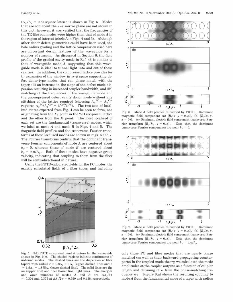
(Lx /Lz 5 0.8) square lattice is shown in Fig. 5. Modesthat are odd about the x –z mirror plane are not shown inthis plot; however, it was verified that the frequencies ofthe TE-like odd modes were higher than that of mode A inthe region of interest (circle A in Figs. 4 and 5). Althoughother donor defect geometries could have been used, thehole radius grading and the lattice compression used hereare important design features of the waveguide for anumber of reasons. As discussed in Section 6, the fieldprofile of the graded cavity mode in Ref. 43 is similar tothat of waveguide mode A, suggesting that this wave-guide mode is ideal to tunnel light into and out of thesecavities. In addition, the compressed lattice provides for(i) expansion of the window in v–b space supporting de-fect donor-type modes that can phase match with thetaper, (ii) an increase in the slope of the defect mode dis-persion resulting in increased coupler bandwidth, and (iii)matching of the frequencies of the waveguide mode andthe uncompressed defect cavity donor mode without anystitching of the lattice required (choosing Lx
PC 5 LxCav
requires LzPC/Lz
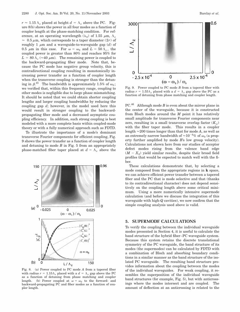
Cav 5 vCav/vPC). The two sets of local-ized states expected from Fig. 4 can be seen to form, oneoriginating from the X1 point in the 2-D reciprocal latticeand the other from the M point. The most localized ofeach set are the fundamental (transverse) modes, whichwe label as mode A and mode B in Figs. 4 and 5. Themagnetic field profiles and the transverse Fourier trans-forms of these localized modes are shown in Figs. 6 and 7.The Fourier transforms confirm that the dominant trans-verse Fourier components of mode A are centered aboutkx 5 0, whereas those of mode B are centered aboutkx 5 6p/Lx . Both of these modes have negative groupvelocity, indicating that coupling to them from the fiberwill be contradirectional in nature.
Using the FDTD-calculated fields for the PC modes, theexactly calculated fields of a fiber taper, and including
Fig. 5. 3-D FDTD calculated band structure for the waveguideshown in Fig. 1(c). The shaded regions indicate continuums ofunbound modes. The dashed lines are the dispersion of fibertapers with radius r 5 0.8Lz 5 1Lx (upper dashed line) and r5 1.5Lz 5 1.875Lx (lower dashed line). The solid lines are the
air (upper line) and fiber (lower line) light lines. The energiesand wave numbers of modes A and B are vLz/2p5 0.304 and 0.373 at bLz/2p 5 0.350 and 0.438, respectively.
only those PC and fiber modes that are nearly phasematched (as well as their backward-propagating counter-parts) in the coupled-mode theory, we calculated the modeamplitudes at the coupler outputs as a function of couplerlength and detuning of v from the phase-matching fre-quency v0 . Figure 8(a) shows the resulting coupling tomode A from the fundamental mode of a taper with radius
Fig. 6. Mode A field profiles calculated by FDTD. Dominantmagnetic field component (a) uBy(x, y 5 0, z)u, (b) uBy(x, y,z 5 0)u. (c) Dominant electric field component transverse Fou-rier transform uEx(kx , y 5 0, z)u. Note that the dominanttransverse Fourier components are near kx 5 0.
Fig. 7. Mode B field profiles calculated by FDTD. Dominantmagnetic field component (a) uBy(x, y 5 0, z)u, (b) uBy(x, y,z 5 0)u. (c) Dominant electric field component transverse Fou-rier transform uEx(kx , y 5 0, z)u. Note that the dominanttransverse Fourier components are near kx 5 6p/Lx .
2280 J. Opt. Soc. Am. B/Vol. 20, No. 11 /November 2003 Barclay et al.
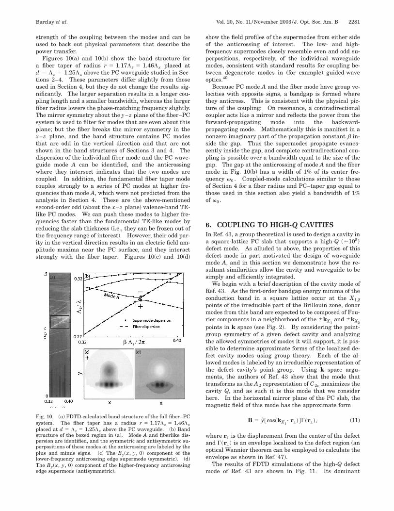
r ' 1.15 Lx placed at height d 5 Lx above the PC. Fig-ure 8(b) shows the power in all four modes as a function ofcoupler length at the phase-matching condition. For ref-erence, at an operating wavelength (l0) of 1.55 mm, Lx' 0.5 mm, which corresponds to a taper diameter (2r) ofroughly 1 mm and a waveguide-to-waveguide gap (d) of0.5 mm in this case. For v 5 v0 and L 5 50 Lz , thecoupled power is greater than 80% and reaches 95% forL 5 80 Lz ('40 mm). The remaining power is coupled tothe backward-propagating fiber mode. Note that, be-cause the PC mode has negative group velocity, this iscontradirectional coupling resulting in monotonically in-creasing power transfer as a function of coupler lengthwhen the transverse coupling is stronger than the detun-ing in b.45 The bandwidth is approximately 1.5% of v0 ;we verified that, within this frequency range, coupling toother modes is negligible due to large phase mismatching.It should be noted that we could obtain shorter couplinglengths and larger coupling bandwidths by reducing thecoupling gap d; however, in the model used here thiswould result in stronger coupling to the backward-propagating fiber mode and a decreased asymptotic cou-pling efficiency. In addition, such strong coupling is bestmodeled with a more complete basis within coupled-modetheory or with a fully numerical approach such as FDTD.
To illustrate the importance of a mode’s dominanttransverse Fourier components for efficient coupling, Fig.9 shows the power transfer as a function of coupler lengthand detuning to mode B in Fig. 5 from an appropriatelyphase-matched fiber taper placed at d 5 Lx above the
Fig. 8. (a) Power coupled to PC mode A from a tapered fiberwith radius r 5 1.15Lx placed with a d 5 Lx gap above the PCas a function of detuning from phase matching and couplerlength. (b) Power coupled at v 5 v0 to the forward- andbackward-propagating PC and fiber modes as a function of cou-pler length.
PC.46 Although mode B is even about the mirror plane inthe center of the waveguide, because it is constructedfrom Bloch modes around the M point it has relativelysmall amplitude for transverse Fourier components nearzero, resulting in a small transverse overlap factor (Kij)with the fiber taper mode. This results in a couplerlength '200 times longer than that for mode A, as well asan extremely narrow bandwidth of '1024% of v0 (a prop-erty further amplified by mode B’s low group velocity).Calculations not shown here from our studies of acceptordefect modes rising from the valence band edge(M 2 X2) yield similar results, despite their broad fieldprofiles that would be expected to match well with the fi-ber.
These calculations demonstrate that, by selecting amode composed from the appropriate regions in k space,we can achieve efficient power transfer between a taperedfiber and the PC that is mode selective and that (thanksto its contradirectional character) does not depend sensi-tively on the coupling length above some critical mini-mum. Using a more numerically intensive supermodecalculation (and before we discuss the integration of thiswaveguide with high-Q cavities), we now confirm that thesimple coupling analysis used above is valid.
5. SUPERMODE CALCULATIONSTo verify the coupling between the individual waveguidemodes presented in Section 4, it is useful to calculate theband structure of the hybrid fiber–PC waveguide system.Because this system retains the discrete translationalsymmetry of the PC waveguide, the band structure of itsmodes (the supermodes) can be calculated by FDTD witha combination of Bloch and absorbing boundary condi-tions in a similar manner as the band structure of the iso-lated PC waveguide. The resulting band structure pro-vides information about the coupling between the modesof the individual waveguides. For weak coupling, it re-sembles the superposition of the individual waveguideband structures (for example, Fig. 5), but with anticross-ings where the modes intersect and are coupled. Theamount of deflection at an anticrossing is related to the
Fig. 9. Power coupled to PC mode B from a tapered fiber withradius r 5 1.55Lx placed with a d 5 Lx gap above the PC as afunction of detuning from phase matching and coupler length.
Barclay et al. Vol. 20, No. 11 /November 2003 /J. Opt. Soc. Am. B 2281
strength of the coupling between the modes and can beused to back out physical parameters that describe thepower transfer.
Figures 10(a) and 10(b) show the band structure fora fiber taper of radius r 5 1.17Lz 5 1.46Lx placed atd 5 Lz 5 1.25Lx above the PC waveguide studied in Sec-tions 2–4. These parameters differ slightly from thoseused in Section 4, but they do not change the results sig-nificantly. The larger separation results in a longer cou-pling length and a smaller bandwidth, whereas the largerfiber radius lowers the phase-matching frequency slightly.The mirror symmetry about the y –z plane of the fiber–PCsystem is used to filter for modes that are even about thisplane; but the fiber breaks the mirror symmetry in thex –z plane, and the band structure contains PC modesthat are odd in the vertical direction and that are notshown in the band structures of Sections 3 and 4. Thedispersion of the individual fiber mode and the PC wave-guide mode A can be identified, and the anticrossingwhere they intersect indicates that the two modes arecoupled. In addition, the fundamental fiber taper modecouples strongly to a series of PC modes at higher fre-quencies than mode A, which were not predicted from theanalysis in Section 4. These are the above-mentionedsecond-order odd (about the x –z plane) valence-band TE-like PC modes. We can push these modes to higher fre-quencies faster than the fundamental TE-like modes byreducing the slab thickness (i.e., they can be frozen out ofthe frequency range of interest). However, their odd par-ity in the vertical direction results in an electric field am-plitude maxima near the PC surface, and they interactstrongly with the fiber taper. Figures 10(c) and 10(d)
Fig. 10. (a) FDTD-calculated band structure of the full fiber–PCsystem. The fiber taper has a radius r 5 1.17Lz 5 1.46Lxplaced at d 5 Lz 5 1.25Lx above the PC waveguide. (b) Bandstructure of the boxed region in (a). Mode A and fiberlike dis-persion are identified, and the symmetric and antisymmetric su-perpositions of these modes at the anticrossing are labeled by theplus and minus signs. (c) The By(x, y, 0) component of thelower-frequency anticrossing edge supermode (symmetric). (d)The By(x, y, 0) component of the higher-frequency anticrossingedge supermode (antisymmetric).
show the field profiles of the supermodes from either sideof the anticrossing of interest. The low- and high-frequency supermodes closely resemble even and odd su-perpositions, respectively, of the individual waveguidemodes, consistent with standard results for coupling be-tween degenerate modes in (for example) guided-waveoptics.40
Because PC mode A and the fiber mode have group ve-locities with opposite signs, a bandgap is formed wherethey anticross. This is consistent with the physical pic-ture of the coupling: On resonance, a contradirectionalcoupler acts like a mirror and reflects the power from theforward-propagating mode into the backward-propagating mode. Mathematically this is manifest in anonzero imaginary part of the propagation constant b in-side the gap. Thus the supermodes propagate evanes-cently inside the gap, and complete contradirectional cou-pling is possible over a bandwidth equal to the size of thegap. The gap at the anticrossing of mode A and the fibermode in Fig. 10(b) has a width of 1% of its center fre-quency v0 . Coupled-mode calculations similar to thoseof Section 4 for a fiber radius and PC–taper gap equal tothose used in this section also yield a bandwidth of 1%of v0 .
6. COUPLING TO HIGH-Q CAVITIESIn Ref. 43, a group theoretical is used to design a cavity ina square-lattice PC slab that supports a high-Q ('105)defect mode. As alluded to above, the properties of thisdefect mode in part motivated the design of waveguidemode A, and in this section we demonstrate how the re-sultant similarities allow the cavity and waveguide to besimply and efficiently integrated.
We begin with a brief description of the cavity mode ofRef. 43. As the first-order bandgap energy minima of theconduction band in a square lattice occur at the X1,2points of the irreducible part of the Brillouin zone, donormodes from this band are expected to be composed of Fou-rier components in a neighborhood of the 6kX1
and 6kX2
points in k space (see Fig. 2). By considering the point-group symmetry of a given defect cavity and analyzingthe allowed symmetries of modes it will support, it is pos-sible to determine approximate forms of the localized de-fect cavity modes using group theory. Each of the al-lowed modes is labeled by an irreducible representation ofthe defect cavity’s point group. Using k space argu-ments, the authors of Ref. 43 show that the mode thattransforms as the A2 representation of C2v maximizes thecavity Q, and as such it is this mode that we considerhere. In the horizontal mirror plane of the PC slab, themagnetic field of this mode has the approximate form
B 5 y@cos~kX1– r'!#G~r'!, (11)
where r' is the displacement from the center of the defectand G(r') is an envelope localized to the defect region (anoptical Wannier theorem can be employed to calculate theenvelope as shown in Ref. 47).
The results of FDTD simulations of the high-Q defectmode of Ref. 43 are shown in Fig. 11. Its dominant
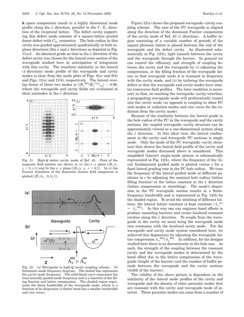
2282 J. Opt. Soc. Am. B/Vol. 20, No. 11 /November 2003 Barclay et al.
k space components result in a highly directional modeprofile along the z direction, parallel to the G –X1 direc-tion of the reciprocal lattice. The defect cavity support-ing this defect mode consists of a square-lattice gradeddonor defect with C2v symmetry. The hole radius in thiscavity was graded approximately quadratically in both in-plane directions [the x and z directions as depicted in Fig.11(a)]. An identical grade as that in the x direction of thedefect cavity was chosen for the lateral cross section of thewaveguide studied here in anticipation of integrationwith this cavity. The resultant similarity in the lateral( x-direction) mode profile of the waveguide and cavitymodes is clear from the mode plots of Figs. 6(a) and 6(b)and Figs. 11(a) and 11(b), respectively. The lateral over-lap factor of these two modes is u^By
WGuByCav&xyu ; 0.98,
where the waveguide and cavity fields are evaluated attheir antinodes in the z direction.
Fig. 11. High-Q defect cavity mode of Ref. 43. Plots of themagnetic field pattern are shown in (a) the x –z plane @ uBy(x,y 5 0, z)u# and (b) the x –y plane @ uBy(x, y, z 5 0)u#. In (c) theFourier transform of the dominant electric field component isplotted @ uEx(kx , 0, kz)u#.
Fig. 12. (a) Waveguide to high-Q cavity coupling scheme. (b)Schematic mode frequency diagram. The dotted line representsthe cavity mode frequency. The solid black curve represents thelocal laterally guided-mode frequency and is a function of the fill-ing fraction and lattice compression. The shaded region repre-sents the finite bandwidth of the waveguide mode, which is afunction of its dispersion (a flatter band has a smaller bandwidthand vice versa).
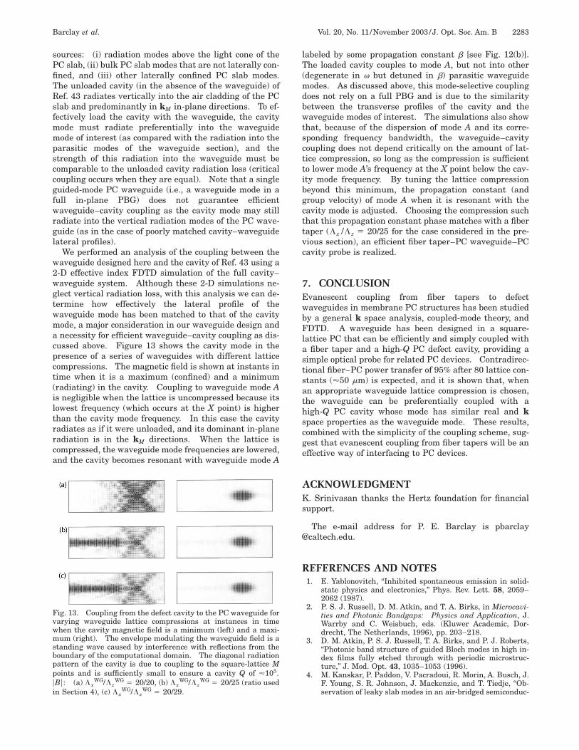
Figure 12(a) shows the proposed waveguide–cavity cou-pling scheme. The axis of the PC waveguide is alignedalong the direction of the dominant Fourier componentsof the cavity mode of Ref. 43 ( z direction). A buffer re-gion consisting of a variable number of periods of thesquare photonic lattice is placed between the end of thewaveguide and the defect cavity. As illustrated sche-matically in Fig. 12(b), light tunnels between the cavityand the waveguide through the barrier. In general wecan control the efficiency and strength of coupling be-tween the cavity and the waveguide by (i) adjusting thecompression, or the filling fraction of the waveguide lat-tice so that waveguide mode A is resonant in frequencywith the cavity mode, and (ii) by tailoring the waveguidedefect so that the waveguide and cavity modes have simi-lar transverse field profiles. The later condition is neces-sary so that, on reaching the waveguide–cavity interface,a propagating waveguide mode will preferentially tunnelinto the cavity mode (as opposed to coupling to other PCslab modes or radiation modes and vice versa for the ra-diation from the cavity mode).
Because of the similarity between the lateral grade inthe hole radius of the PC in the waveguide and the cavitysections, the coupled waveguide–cavity structure can beapproximately viewed as a one-dimensional system alongthe z direction. In this ideal view, the lateral confine-ment in the cavity and waveguide PC sections is singlemode. Only the mode of the PC waveguide–cavity struc-ture that shares the lateral field profile of the cavity andwaveguide modes discussed above is considered. Thissimplified (lateral) single-mode picture is schematicallyrepresented in Fig. 12(b), where the frequency of the (lo-cal) fundamental guided mode is plotted versus z for afixed lateral grading rate in the PC hole radius. We tunethe frequency of the lateral guided mode at different po-sitions in z by adjusting the nominal hole radius (latticefilling fraction) or the lattice constant in the z direction(lattice compression or stretching). The mode’s disper-sion in the PC waveguide section results in a finite-frequency bandwidth and is represented in Fig. 12(b) bythe shaded region. To avoid the stitching of different lat-tices, the lateral lattice constant is kept constant (Lx
cav
5 LxWG). In this way one can engineer band offsets to
produce tunneling barriers and create localized resonantcavities along the z direction. To couple from the wave-guide to the cavity we must bring the waveguide modeinto resonance with the localized cavity mode. For thewaveguide and cavity mode system considered here, weachieved this degeneracy by adjusting the waveguide lat-tice compression Lx
WG/LzWG. In addition, for the designs
studied here there is no discontinuity in the hole size. Assuch, the strength of the coupling between the resonantcavity and the waveguide modes is determined by theband offset due to the lattice compression of the wave-guide (height of the barrier) and the number of buffer pe-riods between the waveguide and the cavity sections(width of the barrier).
The validity of the above picture is dependent on thesimilarity of the lateral mode profiles of the cavity andwaveguide and the density of other parasitic modes thatare resonant with the cavity and waveguide mode of in-terest. These parasitic modes can come from a number of
Barclay et al. Vol. 20, No. 11 /November 2003 /J. Opt. Soc. Am. B 2283
sources: (i) radiation modes above the light cone of thePC slab, (ii) bulk PC slab modes that are not laterally con-fined, and (iii) other laterally confined PC slab modes.The unloaded cavity (in the absence of the waveguide) ofRef. 43 radiates vertically into the air cladding of the PCslab and predominantly in kM in-plane directions. To ef-fectively load the cavity with the waveguide, the cavitymode must radiate preferentially into the waveguidemode of interest (as compared with the radiation into theparasitic modes of the waveguide section), and thestrength of this radiation into the waveguide must becomparable to the unloaded cavity radiation loss (criticalcoupling occurs when they are equal). Note that a singleguided-mode PC waveguide (i.e., a waveguide mode in afull in-plane PBG) does not guarantee efficientwaveguide–cavity coupling as the cavity mode may stillradiate into the vertical radiation modes of the PC wave-guide (as in the case of poorly matched cavity–waveguidelateral profiles).
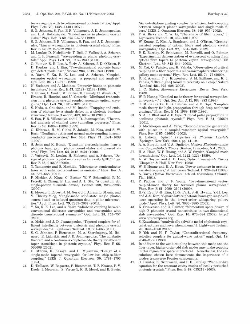
We performed an analysis of the coupling between thewaveguide designed here and the cavity of Ref. 43 using a2-D effective index FDTD simulation of the full cavity–waveguide system. Although these 2-D simulations ne-glect vertical radiation loss, with this analysis we can de-termine how effectively the lateral profile of thewaveguide mode has been matched to that of the cavitymode, a major consideration in our waveguide design anda necessity for efficient waveguide–cavity coupling as dis-cussed above. Figure 13 shows the cavity mode in thepresence of a series of waveguides with different latticecompressions. The magnetic field is shown at instants intime when it is a maximum (confined) and a minimum(radiating) in the cavity. Coupling to waveguide mode Ais negligible when the lattice is uncompressed because itslowest frequency (which occurs at the X point) is higherthan the cavity mode frequency. In this case the cavityradiates as if it were unloaded, and its dominant in-planeradiation is in the kM directions. When the lattice iscompressed, the waveguide mode frequencies are lowered,and the cavity becomes resonant with waveguide mode A
Fig. 13. Coupling from the defect cavity to the PC waveguide forvarying waveguide lattice compressions at instances in timewhen the cavity magnetic field is a minimum (left) and a maxi-mum (right). The envelope modulating the waveguide field is astanding wave caused by interference with reflections from theboundary of the computational domain. The diagonal radiationpattern of the cavity is due to coupling to the square-lattice Mpoints and is sufficiently small to ensure a cavity Q of '105.uBu: (a) Lx
WG/LzWG 5 20/20, (b) Lx
WG/LzWG 5 20/25 (ratio used
in Section 4), (c) LxWG/Lz
WG 5 20/29.
labeled by some propagation constant b [see Fig. 12(b)].The loaded cavity couples to mode A, but not into other(degenerate in v but detuned in b) parasitic waveguidemodes. As discussed above, this mode-selective couplingdoes not rely on a full PBG and is due to the similaritybetween the transverse profiles of the cavity and thewaveguide modes of interest. The simulations also showthat, because of the dispersion of mode A and its corre-sponding frequency bandwidth, the waveguide–cavitycoupling does not depend critically on the amount of lat-tice compression, so long as the compression is sufficientto lower mode A’s frequency at the X point below the cav-ity mode frequency. By tuning the lattice compressionbeyond this minimum, the propagation constant (andgroup velocity) of mode A when it is resonant with thecavity mode is adjusted. Choosing the compression suchthat this propagation constant phase matches with a fibertaper (Lx /Lz 5 20/25 for the case considered in the pre-vious section), an efficient fiber taper–PC waveguide–PCcavity probe is realized.
7. CONCLUSIONEvanescent coupling from fiber tapers to defectwaveguides in membrane PC structures has been studiedby a general k space analysis, coupled-mode theory, andFDTD. A waveguide has been designed in a square-lattice PC that can be efficiently and simply coupled witha fiber taper and a high-Q PC defect cavity, providing asimple optical probe for related PC devices. Contradirec-tional fiber–PC power transfer of 95% after 80 lattice con-stants ('50 mm) is expected, and it is shown that, whenan appropriate waveguide lattice compression is chosen,the waveguide can be preferentially coupled with ahigh-Q PC cavity whose mode has similar real and kspace properties as the waveguide mode. These results,combined with the simplicity of the coupling scheme, sug-gest that evanescent coupling from fiber tapers will be aneffective way of interfacing to PC devices.
ACKNOWLEDGMENTK. Srinivasan thanks the Hertz foundation for financialsupport.
The e-mail address for P. E. Barclay is [email protected].
REFERENCES AND NOTES1. E. Yablonovitch, ‘‘Inhibited spontaneous emission in solid-
state physics and electronics,’’ Phys. Rev. Lett. 58, 2059–2062 (1987).
2. P. S. J. Russell, D. M. Atkin, and T. A. Birks, in Microcavi-ties and Photonic Bandgaps: Physics and Application, J.Warrby and C. Weisbuch, eds. (Kluwer Academic, Dor-drecht, The Netherlands, 1996), pp. 203–218.
3. D. M. Atkin, P. S. J. Russell, T. A. Birks, and P. J. Roberts,‘‘Photonic band structure of guided Bloch modes in high in-dex films fully etched through with periodic microstruc-ture,’’ J. Mod. Opt. 43, 1035–1053 (1996).
4. M. Kanskar, P. Paddon, V. Pacradoui, R. Morin, A. Busch, J.F. Young, S. R. Johnson, J. Mackenzie, and T. Tiedje, ‘‘Ob-servation of leaky slab modes in an air-bridged semiconduc-
2284 J. Opt. Soc. Am. B/Vol. 20, No. 11 /November 2003 Barclay et al.
tor waveguide with two-dimensional photonic lattice,’’ Appl.Phys. Lett. 70, 1438–1440 (1997).
5. S. G. Johnson, S. Fan, P. R. Villeneuve, J. D. Joannopoulos,and L. A. Kolodziejaki, ‘‘Guided modes in photonic crystalslabs,’’ Phys. Rev. B 60, 5751–5758 (1999).
6. S. G. Johnson, P. R. Villeneuve, S. Fan, and J. D. Joannopo-ulos, ‘‘Linear waveguides in photonic-crystal slabs,’’ Phys.Rev. B 62, 8212–8222 (2000).
7. M. Loncar, D. Nedeljkovic, T. Doll, J. Vuckovic, A. Scherer,and T. P. Pearsall, ‘‘Waveguiding in planar photonic crys-tals,’’ Appl. Phys. Lett. 77, 1937–1939 (2000).
8. O. Painter, R. K. Lee, A. Yariv, A. Scherer, J. D. O’Brien, P.D. Dapkus, and I. Kim, ‘‘Two-dimensional photonic band-gap defect mode laser,’’ Science 284, 1819–1824 (1999).
9. A. Yariv, Y. Xu, R. K. Lee, and A. Scherer, ‘‘Coupled-resonator optical waveguide: a proposal and analysis,’’Opt. Lett. 24, 711–713 (1999).
10. N. Stefanou and A. Modinos, ‘‘Impurity bands in photonicinsulators,’’ Phys. Rev. B 57, 12127–12133 (1998).
11. S. Olivier, C. Smith, M. Rattier, H. Benisty, C. Weisbuch, T.Krauss, R. Houdre, and U. Oesterle, ‘‘Miniband transmis-sion in a photonic crystal coupled-resonator optical wave-guide,’’ Opt. Lett. 26, 1019–1021 (2001).
12. S. Noda, A. Chutinan, and M. Imada, ‘‘Trapping and emis-sion of photons by a single defect in a photonic bandgapstructure,’’ Nature (London) 407, 608–610 (2000).
13. S. Fan, P. R. Villeneuve, and J. D. Joannopoulos, ‘‘Theoret-ical analysis of channel drop tunneling processes,’’ Phys.Rev. B 59, 15882–15892 (1999).
14. G. Khitrova, H. M. Gibbs, F. Jahnke, M. Kira, and S. W.Koch, ‘‘Nonlinear optics and normal-mode-coupling in semi-conductor microcavities,’’ Rev. Mod. Phys. 71, 1591–1639(1999).
15. S. John and K. Busch, ‘‘Quantum electrodynamics near aphotonic band gap: photon bound states and dressed at-oms,’’ Phys. Rev. Lett. 64, 2418–2421 (1990).
16. J. Vuckovic, M. Loncar, H. Mabuchi, and A. Scherer, ‘‘De-sign of photonic crystal microcavites for cavity QED,’’ Phys.Rev. E 65, 016608 (2002).
17. Y. Yamamoto and S. Machida, ‘‘Microcavity semiconductorlaser with enhanced spontaneous emission,’’ Phys. Rev. A44, 657–668 (1991).
18. P. Michler, A. Kiraz, C. Becher, W. V. Schoenfeld, P. M.Petroff, L. Zhang, E. Hu, and A. I. Glu, ‘‘A quantum dotsingle-photon turnstile device,’’ Science 290, 2282–2285(2000).
19. E. Moreau, I. Robert, J. M. Gerard, I. Abram, L. Manin, andV. Thierry-Mieg, ‘‘Single-mode solid-state single photonsource based on isolated quantum dots in pillar microcavi-ties,’’ Appl. Phys. Lett. 79, 2865–2867 (2001).
20. Y. Xu, R. K. Lee, and A. Yariv, ‘‘Adiabatic coupling betweenconventional dielectric waveguides and waveguides withdiscrete translational symmetry,’’ Opt. Lett. 25, 755–757(2000).
21. A. Mekis and J. D. Joannopoulos, ‘‘Tapered couplers for ef-ficient interfacing between dielectric and photonic crystalwaveguides,’’ J. Lightwave Technol. 19, 861–865 (2001).
22. S. G. Johnson, P. Bienstman, M. A. Skorobogatiy, M. Iba-nescu, E. Lidorikis, and J. D. Joannopoulos, ‘‘The adiabatictheorem and a continuous coupled-mode theory for efficienttaper transitions in photonic crystals,’’ Phys. Rev. E 66,066608 (2002).
23. O. Mitomi, K. Kasaya, and H. Miyazawa, ‘‘Design of asingle-mode tapered waveguide for low-loss chip-to-fibercoupling,’’ IEEE J. Quantum Electron. 30, 1787–1793(1994).
24. D. Taillaert, W. Bogaerts, P. Bienstman, T. F. Krauss, P. V.Daele, I. Moerman, S. Vertuyft, K. D. Mesel, and R. Baets,
‘‘An out-of-plane grating coupler for efficient butt-couplingbetween compact planar waveguides and single-mode fi-bers,’’ IEEE J. Quantum Electron. 38, 949–955 (2002).
25. T. A. Birks and Y. W. Li, ‘‘The shape of fiber tapers,’’ J.Lightwave Technol. 10, 432–438 (1992).
26. W. Kuang, C. Kim, A. Stapleton, and J. O’Brien, ‘‘Grating-assisted coupling of optical fibers and photonic crystalwaveguides,’’ Opt. Lett. 27, 1604–1606 (2002).
27. P. E. Barclay, K. Srinivasan, M. Borselli, and O. Painter,‘‘Experimental demonstration of evanescent coupling fromoptical fibre tapers to photonic crystal waveguides,’’ IEEElectron. Lett. 39, 842–844 (2003).
28. M. Cai, O. Painter, and K. Vahala, ‘‘Observation of criticalcoupling in a fiber taper to a silica-microsphere whispering-gallery mode system,’’ Phys. Rev. Lett. 85, 74–77 (2000).
29. D. K. Armani, T. J. Kippenberg, S. M. Spillane, and K. J.Vahala, ‘‘Ultra-high-Q toroid microcavity on a chip,’’ Nature(London) 421, 925–928 (2003).
30. J. C. Slater, Microwave Electronics (Dover, New York,1969).
31. W.-P. Huang, ‘‘Coupled-mode theory for optical waveguides:an overview,’’ J. Opt. Soc. Am. A 11, 963–983 (1994).
32. C. M. de Sterke, D. G. Salinas, and J. E. Sipe, ‘‘Coupled-mode theory for light propagation through deep nonlineargratings,’’ Phys. Rev. E 54, 1969–1989 (1996).
33. N. A. R. Bhat and J. E. Sipe, ‘‘Optical pulse propagation innonlinear photonic crystals,’’ Phys. Rev. E 64, 056604(2001).
34. S. Mookherjea and A. Yariv, ‘‘Second-harmonic generationwith pulses in a coupled-resonator optical waveguide,’’Phys. Rev. E 65, 026607 (2002).
35. K. Sakoda, Optical Properties of Photonic Crystals(Springer, New York, 2001), pp. 14–19.
36. A. A. Barybin and V. A. Dmitriev, Modern Electrodynamicsand Coupled-Mode Theory (Rinton, Princeton, N.J., 2002).
37. H. A. Haus, W. P. Huang, and A. W. Snyder, ‘‘Coupled-modeformulations,’’ Opt. Lett. 14, 1222–1224 (1989).
38. A. W. Snyder and J. D. Love, Optical Waveguide Theory(Chapman & Hall, New York, 1983).
39. W. P. Huang and H. A. Haus, ‘‘Power exchange in grating-assisted couplers,’’ J. Lightwave Technol. 7, 920–924 (1989).
40. A. Yariv, Optical Electronics, 4th ed. (Saunders, Orlando,Fla., 1991).
41. P. Paddon and J. F. Young, ‘‘Two-dimensional vector-coupled-mode theory for textured planar waveguides,’’Phys. Rev. B 61, 2090–2101 (2000).
42. H.-Y. Ryu, S.-H. Kim, H.-G. Park, J.-K. Hwang, Y.-H. Lee,and J.-S. Kim, ‘‘Square-lattice photonic band-gap single-celllaser operating in the lowest-order whispering gallerymode,’’ Appl. Phys. Lett. 80, 3883–3885 (2002).
43. K. Srinivasan and O. Painter, ‘‘Momentum space design ofhigh-Q photonic crystal nanocavities in two-dimensionalslab waveguides,’’ Opt. Exp. 10, 670–684 (2002), http://www.opticsexpress.org.
44. S. Kawakami, ‘‘Analytically solvable model of photonic crys-tal structures and novel phenomena,’’ J. Lightwave Technol.20, 1644–1650 (2002).
45. P. Yeh and H. F. Taylor, ‘‘Contradirectional frequency-selectice couplers for guided-wave optics,’’ Appl. Opt. 19,2848–2855 (1980).
46. In addition to the weak coupling between this mode and thefiber taper, higher-order odd slab modes may make couplingin this region of k space impractical. Nonetheless, the cal-culations shown here demonstrate the importance of amode’s transverse Fourier components.
47. O. Painter, K. Srinivasan, and P. E. Barclay, ‘‘Wannier-likeequation for the resonant cavity modes of locally perturbedphotonic crystals,’’ Phys. Rev. B 68, 035214 (2003).