design project basics - college of engineering, …€“ 30% final demo evaluation – 20% report...
TRANSCRIPT
ECE 410, Prof. A. Mason Design Project, Page 1
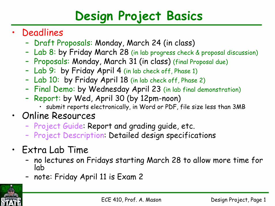
Design Project Basics• Deadlines
– Draft Proposals: Monday, March 24 (in class) – Lab 8: by Friday March 28 (in lab progress check & proposal discussion)– Proposals: Monday, March 31 (in class) (final Proposal due)– Lab 9: by Friday April 4 (in lab check off, Phase 1)– Lab 10: by Friday April 18 (in lab check off, Phase 2)– Final Demo: by Wednesday April 23 (in lab final demonstration)– Report: by Wed, April 30 (by 12pm-noon)
• submit reports electronically, in Word or PDF, file size less than 3MB• Online Resources
– Project Guide: Report and grading guide, etc.– Project Description: Detailed design specifications
• Extra Lab Time– no lectures on Fridays starting March 28 to allow more time for
lab– note: Friday April 11 is Exam 2

ECE 410, Prof. A. Mason Design Project, Page 2
Design Project Grading• The combined components of the Design Project
are worth 25% of your overall class grade.• Design Project grade will be broken down as:
– 10% Quality of Proposal– 30% Lab 8-10 Evaluations– 30% Final Demo Evaluation– 20% Report Quality– 10% Individual Effort

ECE 410, Prof. A. Mason Design Project, Page 3
Design Project Overview• Project Focus
– design a custom CMOS microprocessor data path• Data Path Components
– ALU (logic & arithmetic)– Shifter– Register File (memory)
ECE 410, Prof. A. Mason Design Project, Page 4
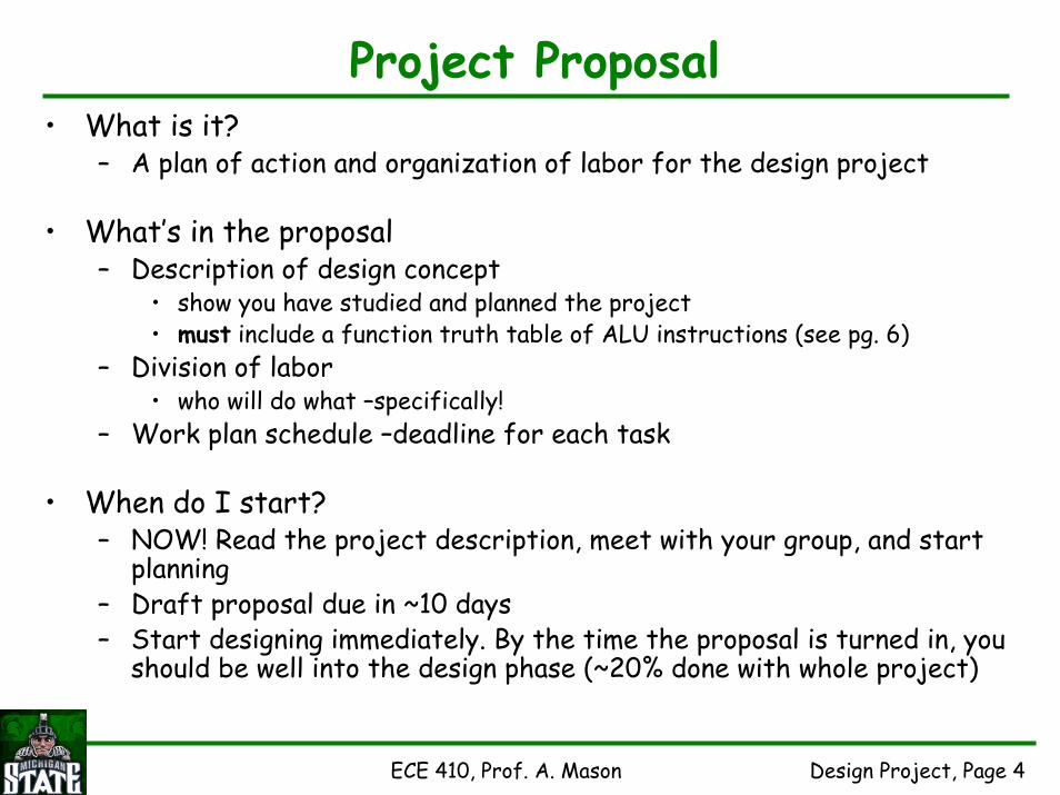
Project Proposal• What is it?
– A plan of action and organization of labor for the design project
• What’s in the proposal– Description of design concept
• show you have studied and planned the project• must include a function truth table of ALU instructions (see pg. 6)
– Division of labor• who will do what –specifically!
– Work plan schedule –deadline for each task
• When do I start?– NOW! Read the project description, meet with your group, and start
planning– Draft proposal due in ~10 days– Start designing immediately. By the time the proposal is turned in, you
should be well into the design phase (~20% done with whole project)
ECE 410, Prof. A. Mason Design Project, Page 5
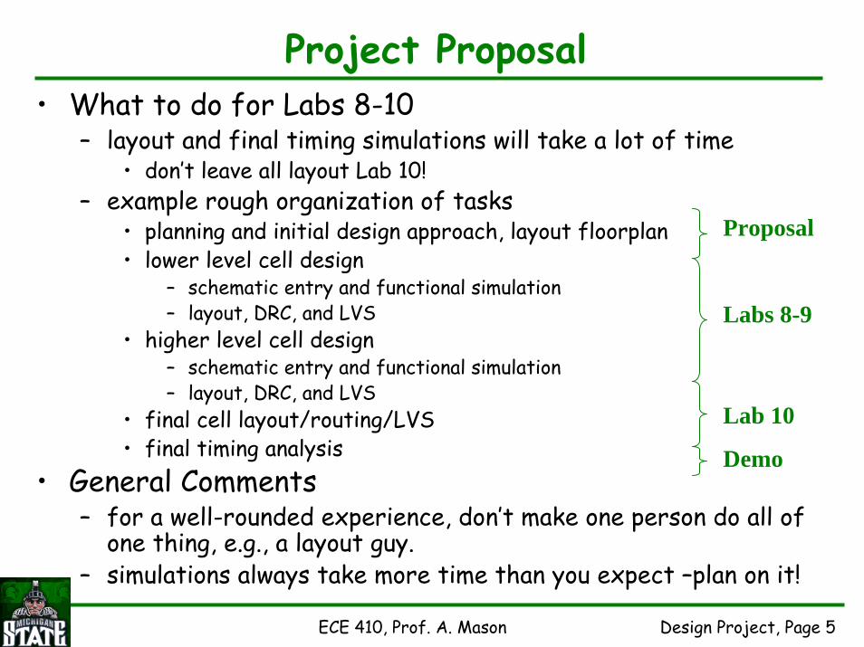
Project Proposal• What to do for Labs 8-10
– layout and final timing simulations will take a lot of time• don’t leave all layout Lab 10!
– example rough organization of tasks• planning and initial design approach, layout floorplan• lower level cell design
– schematic entry and functional simulation– layout, DRC, and LVS
• higher level cell design– schematic entry and functional simulation– layout, DRC, and LVS
• final cell layout/routing/LVS• final timing analysis
• General Comments– for a well-rounded experience, don’t make one person do all of
one thing, e.g., a layout guy.– simulations always take more time than you expect –plan on it!
Proposal
Labs 8-9
Lab 10
Demo
ECE 410, Prof. A. Mason Design Project, Page 6
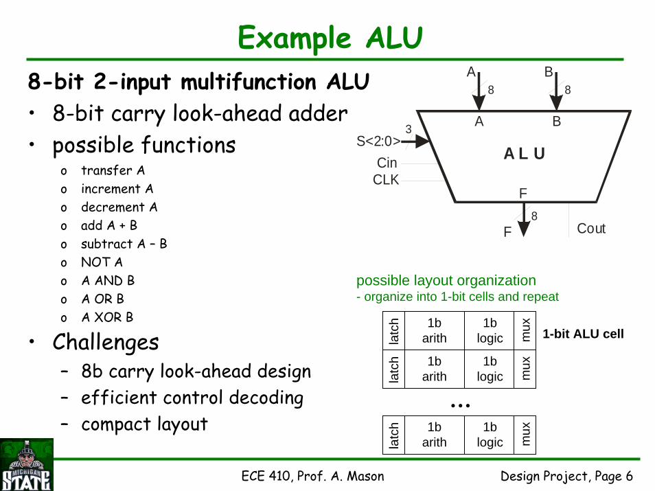
Example ALU8-bit 2-input multifunction ALU• 8-bit carry look-ahead adder• possible functions
o transfer Ao increment Ao decrement Ao add A + Bo subtract A – Bo NOT Ao A AND Bo A OR Bo A XOR B
• Challenges– 8b carry look-ahead design– efficient control decoding– compact layout
8
3
A
A
A L U
F
F Cout
CLKCin
S<2:0>
B
B
8
8
possible layout organization- organize into 1-bit cells and repeat
1barithla
tch 1b
logic mux
1barithla
tch 1b
logic mux
1barithla
tch 1b
logic mux
…
1-bit ALU cell
ECE 410, Prof. A. Mason Design Project, Page 7
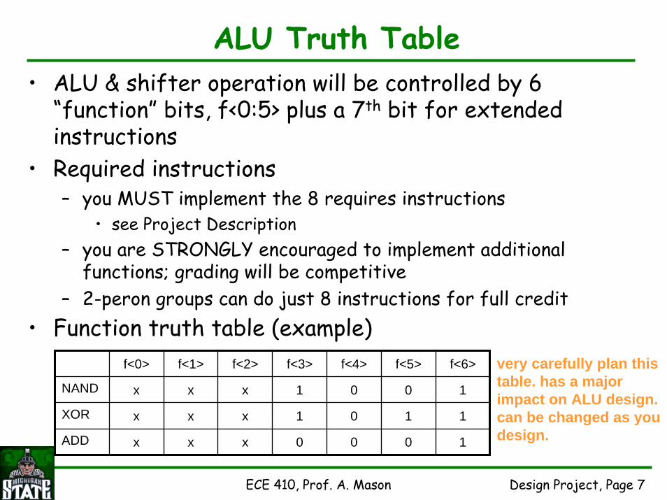
ALU Truth Table• ALU & shifter operation will be controlled by 6
“function” bits, f<0:5> plus a 7th bit for extended instructions
• Required instructions– you MUST implement the 8 requires instructions
• see Project Description– you are STRONGLY encouraged to implement additional
functions; grading will be competitive– 2-peron groups can do just 8 instructions for full credit
• Function truth table (example)f<0> f<1> f<2> f<3> f<4> f<5> f<6>
NAND x x x 1 0 0 1
XOR x x x 1 0 1 1
ADD x x x 0 0 0 1
very carefully plan this table. has a major impact on ALU design.can be changed as youdesign.

ECE 410, Prof. A. Mason Design Project, Page 8
Data Path Physical Design• Organize by bit
latch Register file
latch ALU Shifter
Address ALU op Shift control
latch Register file
latch ALU Shifter
latch Register file
latch ALU ShifterRegister file
latch ALU Shifter
latch Register file
latch ALU Shifterlatch Register file
latch ALU Shifter
......
MUX
MUX
MUX
bit 0
bit 1***
bit 7
ECE 410, Prof. A. Mason Design Project, Page 9
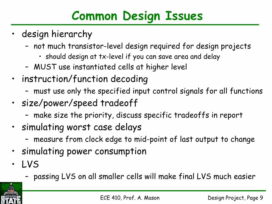
Common Design Issues• design hierarchy
– not much transistor-level design required for design projects• should design at tx-level if you can save area and delay
– MUST use instantiated cells at higher level• instruction/function decoding
– must use only the specified input control signals for all functions• size/power/speed tradeoff
– make size the priority, discuss specific tradeoffs in report• simulating worst case delays
– measure from clock edge to mid-point of last output to change• simulating power consumption• LVS
– passing LVS on all smaller cells will make final LVS much easier

ECE 410, Prof. A. Mason Design Project, Page 10
Group Lab Comments• Teamwork “professional skill”
– valued by employers• Organizing your team/group
– divide and conquer to get started• plan who will do what, organize by email to reduce in-person demand
– work together to learn from each other• after individual effort, meet as pairs or as 3 and have fun learning
• Dividing Work Load– divide by cells– divide by software tools– * don’t assign report to one person
• all should contribute, everyone needs experience writing
• Directory Permissions– anyone having trouble with permission issues?
ECE 410, Prof. A. Mason Design Project, Page 11
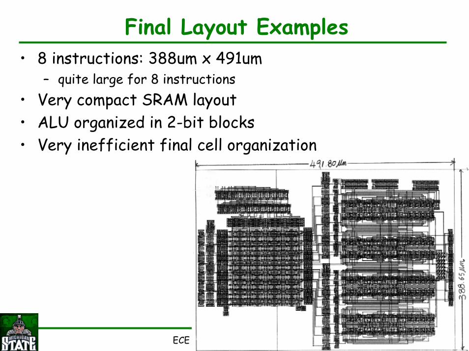
Final Layout Examples• 8 instructions: 388um x 491um
– quite large for 8 instructions• Very compact SRAM layout• ALU organized in 2-bit blocks• Very inefficient final cell organization

ECE 410, Prof. A. Mason Design Project, Page 12
Final Layout Examples• 16-instruction ALU• 280um x 554um
– very small area for 16 instructions• Clearly organized in bit slices
– control decoder on bottom• Very tightly packed transistors within bit slice
• Lots of open area in final cell– could have been better planned to
eliminate wasted chip area
ECE 410, Prof. A. Mason Design Project, Page 13
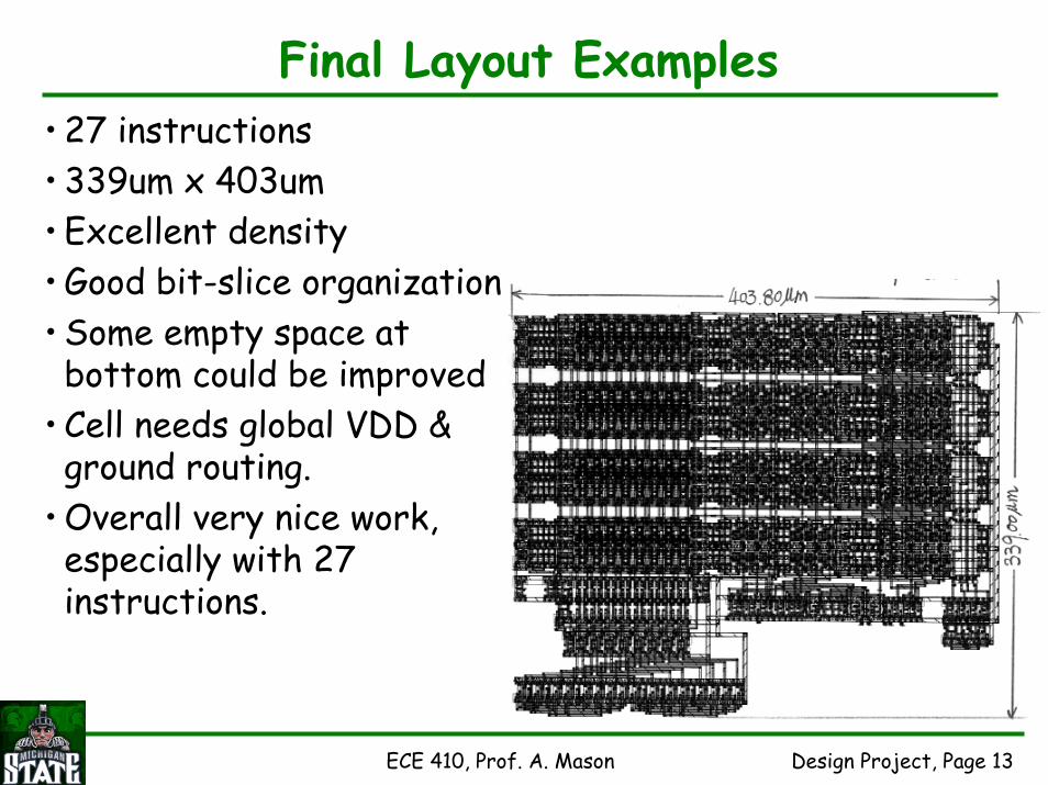
Final Layout Examples• 27 instructions• 339um x 403um• Excellent density• Good bit-slice organization • Some empty space at bottom could be improved
• Cell needs global VDD & ground routing.
• Overall very nice work, especially with 27 instructions.