designing variation-tolerance in mixed-signal components of a system-on-chip wei jiang and vishwani...
TRANSCRIPT

Designing Variation-Tolerance in Mixed-Signal Components of a System-
on-ChipWei Jiang and Vishwani D. Agrawal
Electrical and Computer EngineeringAuburn University, Auburn, AL 36849
[email protected], [email protected]
2009 IEEE International Symposium on Circuits and Systems

Motivation• Process variation in nanoscale technology
– Catastrophic faults– Parametric faults, more than before, cause
• Degraded performance• Yield reduction
• Built-in self-test and self-calibration– Test and diagnosis– Device calibration
• Characteristics measurement• On-chip error correction
ISCAS'09 2

Mixed-Signal Devices Under Test
ISCAS'09 3
Portions of a typical wireless transceiver SOC.
DAC
ADC
MIXED SIGNAL
ANALOG SYSTEM
ANALOG SYSTEM
Digital System
Input and Output
DSP
DIGITAL SYSTEM
Analog System
Input and
Output
Analog output
Analog input
Analog signals
Analog signals
under-test
Digital input
under-test
DevicesUnderTest
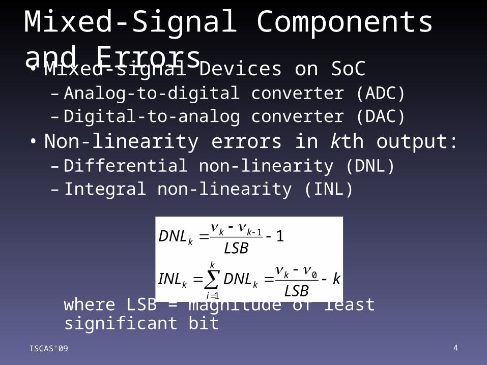
Mixed-Signal Components and Errors• Mixed-signal Devices on SoC
– Analog-to-digital converter (ADC)– Digital-to-analog converter (DAC)
• Non-linearity errors in kth output:– Differential non-linearity (DNL)– Integral non-linearity (INL)
where LSB = magnitude of least significant bitISCAS'09 4
kLSB
DNLINL
LSBDNL
kk
ikk
kkk
0
1
1 1

A Conventional Mixed-Signal BIST Architecture
ISCAS'09 5
See, F. F. Dai and C. E. Stroud, “Analog and Mixed-Signal Test Architectures,” Chapter 15, p. 722 in System-on-Chip Test Architectures: Nanometer Design for Testability, Morgan Kaufmann, 2008.
TPG
ORA
TEST CONTROL
MUX
MUX
DAC
ADC
MIXED SIGNAL
MUX
ANALOG SYSTEM
ANALOG SYSTEM
MUX
BIST Results
Digital System
Input and Output
Analog System
Input and
Output
Analog Loopbacks
DSP
DIGITAL SYSTEM
Digital loopback
Digital input
Loopback controls
Test pattern control
Response control
Digital outputAnalog signals
Analog loopback
Analog system loopback
Analog output
Analog input
under-test
under-test
under-test
DevicesUnderTest
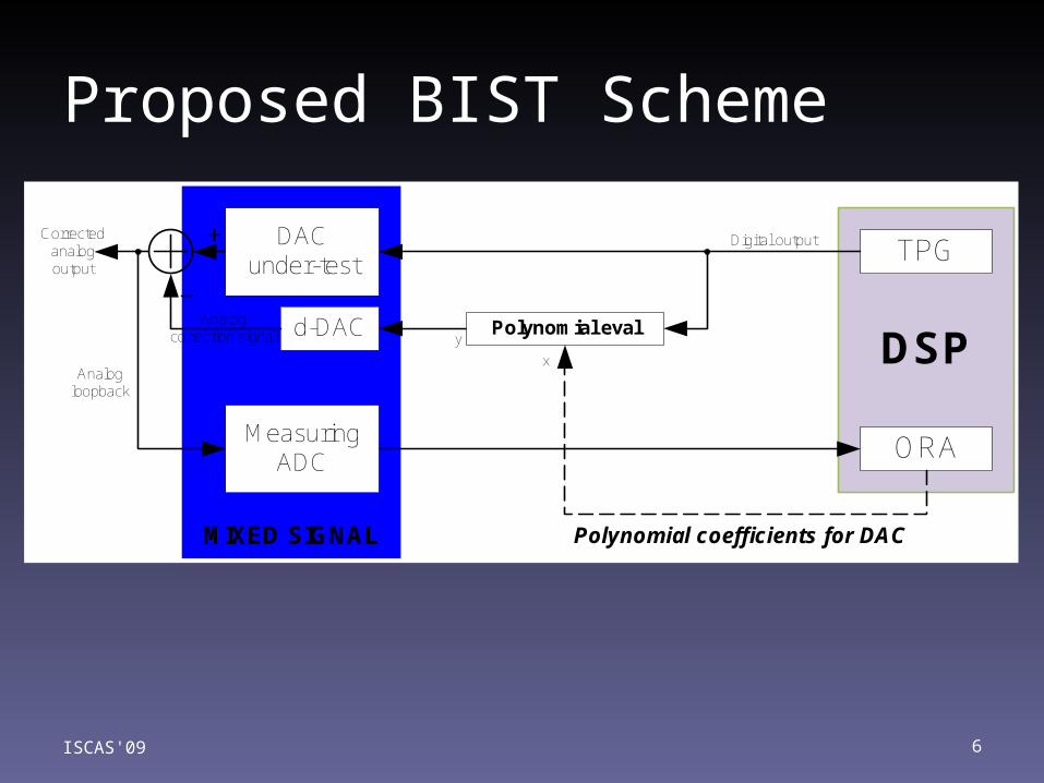
Proposed BIST Scheme
ISCAS'09 6
DSP
TPG
ORA
MIXED SIGNAL Polynomial coefficients for DAC
x
yAnalog
correction signal Polynomial eval
Digital outputCorrected analog output
Analog loopback
DACunder-test
d-DAC
Measuring ADC

DAC Output Measurement (Off-Line)• The on –chip DSP provides all codes to the DAC
under test.• A 1-bit ΣΔ modulator does A-to-D conversion.• High linearity due to oversampling and noise
shaping technique.• Assumption: ΣΔ modulator is fault-free because of
its simple structure and good tolerance for quantization errors.
• ΣΔ is modulator is deactivated during normal system operation; no performance impact on SoC.
• Use of higher-order ΣΔ modulator may have advantages, to be investigated.
ISCAS'09 7
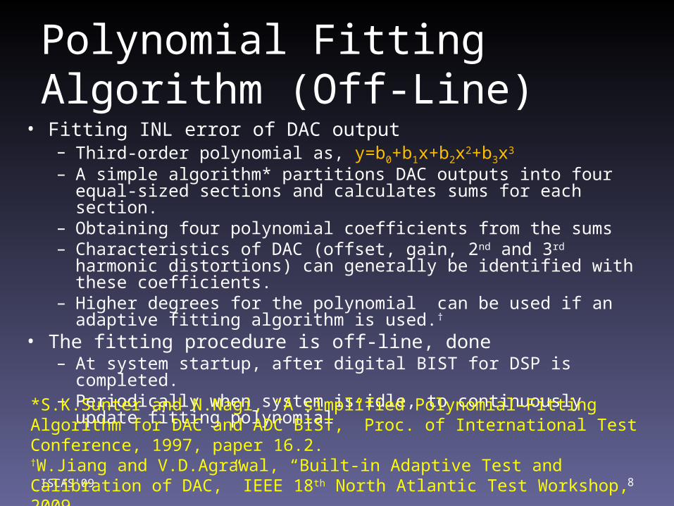
Polynomial Fitting Algorithm (Off-Line)
• Fitting INL error of DAC output– Third-order polynomial as, y=b0+b1x+b2x2+b3x3
– A simple algorithm* partitions DAC outputs into four equal-sized sections and calculates sums for each section.
– Obtaining four polynomial coefficients from the sums– Characteristics of DAC (offset, gain, 2nd and 3rd harmonic distortions)
can generally be identified with these coefficients.– Higher degrees for the polynomial can be used if an adaptive fitting
algorithm is used.†
• The fitting procedure is off-line, done– At system startup, after digital BIST for DSP is completed.– Periodically when system is idle, to continuously update fitting
polynomial
ISCAS'09 8
*S.K.Sunter and N.Nagi, “A simplified Polynomial-Fitting Algorithm for DAC and ADC BIST,” Proc. of International Test Conference, 1997, paper 16.2.†W.Jiang and V.D.Agrawal, “Built-in Adaptive Test and Calibration of DAC,” IEEE 18th North Atlantic Test Workshop, 2009
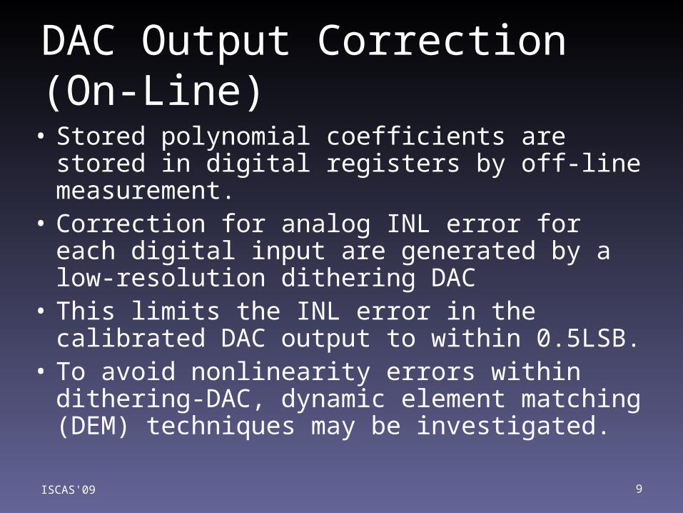
DAC Output Correction (On-Line)• Stored polynomial coefficients are stored in
digital registers by off-line measurement.• Correction for analog INL error for each digital
input are generated by a low-resolution dithering DAC
• This limits the INL error in the calibrated DAC output to within 0.5LSB.
• To avoid nonlinearity errors within dithering-DAC, dynamic element matching (DEM) techniques may be investigated.
ISCAS'09 9

More Details and Subsequent Work• Testing of on-chip ADC:
– Use calibrated DAC to test and characterize on-chip ADC under test.
– For details, see Proc. ISACS09.
– Also see, W.Jiang and V.D.Agrawal, “Built-in Self-Calibration of On-Chip DAC and ADC,” Proc. of International Test Conference, 2008, paper 32.2.
• Later work,– W.Jiang and V.D.Agrawal, “Built-in Adaptive Test
and Calibration of DAC,” Proc. 18th IEEE North Atlantic Test Workshop, May 13-15, 2009, pp. 3-8.
ISCAS'09 10

A 14-Bit DAC with Nonlinearity
ISCAS'09 11
• 16K ramp codes• Maximum INL error up to ±1.5dB
Indices of 14-bit DAC-under-test

Polynomial Fit and Calibrated DAC
ISCAS'09 12
• Polynomial fitting for DAC output
• 6-bit low cost dithering-DAC
• INL error reduced to ±0.5dB
Indices of 14-bit DAC-under-test

Conclusion and Future Work• Proposed technique
– Uses simple devices for a post-fabrication technique to improve system reliability against process-variation.
– Off-line built-in fault-detection and parameter characterization.
– On-line at-speed self-correction for nonlinearity errors.
• Future Work– Reliable self-test for test and calibration circuitry
(sigma-delta modulator, dithering DAC, etc.)– Generalize the polynomial interpolation of INL to
higher degree polynomials.
ISCAS'09 13

Thank you
• Authors will appreciate your questions or comments.
• Please write to:– Wei Jiang, [email protected] – Vishwani D. Agrawal
ISCAS'09 14