determination of bit timing parameters for the can ... · summary determination of bit timing...
TRANSCRIPT

APPLICATION NOTE
Determination of Bit Timing Parameters for the
CAN Controller SJA 1000AN97046
Abstract
Determination of Bit Timing Parameters for the CAN Controller SJA 1000
Philips Semiconductors
Application NoteAN97046
2
Philips Electronics N.V. 1997
All rights are reserved. Reproduction in whole or in part is prohibited without the prior written consent of the copy-right owner.
The information presented in this document does not form part of any quotation or contract, is believed to beaccurate and reliable and may be changed without notice. No liability will be accepted by the publisher for anyconsequence of its use. Publication thereof does not convey nor imply any license under patent- or other indus-trial or intellectual property rights.
The CAN protocol provides for programming of the bit rate, and the number and location of data samples in a bit period. Optimization of these parameters guarantees message synchronization and proper error detection at the extremes of oscillator tolerance and propagation delay. A step by step method for calculating optimum CAN bit timing parameters for a given set of system constraints is presented. Support is given for adjustment of the CAN controllers SJA 1000 and PCx82C200 from Philips Semiconductors. Detailed examples are included as well.

Keywords
Philips Semiconductors
Author(s):
Determination of Bit Timing Parameters for SJA 1000 CAN Controller
Application NoteAN97046
3
APPLICATION NOTE
Determination of Bit Timing Parameters for SJA 1000 CAN Controller
Egon Jöhnk, Klaus Dietmayer
Systems Laboratory Hamburg, Germany
CAN, Bit Timing, Bit Rate, Propagation Delay, Oscillator Frequency,SJA 1000, PCx82C200
Date: 15th July 1997
AN97046

Summary
Determination of Bit Timing Parameters for SJA 1000 CAN Controller
Philips Semiconductors
Application NoteAN97046
4
The Controller Area Network (CAN) is a serial, asynchronous, multi-master communication protocol for connect-ing electronic control modules, sensors and actuators in automotive and industrial applications. A feature of the CAN protocol is that the bit rate, bit sample point and number of samples in a bit period are user programmable. This gives the user the freedom to optimize the performance of the network for his given application. During this optimization process the user has to be aware of the relationship between the bit timing parameters, the refer-ence oscillator tolerance and the various signal propagation delays in the system.
This report focuses on the determination of bit timing parameters for the Philips CAN controllers SJA 1000 and PCx82C200. The basic CAN bit timing relationships are explained, calculation rules are discussed and examples are given with respect to different system requirements. In addition to the sets of equations, graphs and tables are provided allowing an easy graphical determination of bit timing parameters.

Determination of Bit Timing Parameters for SJA 1000 CAN Controller
Philips Semiconductors
5
Application NoteAN97046
CONTENTS
1. INTRODUCTION . . . . . . . . . . . . . . . . . . . . . . . . . . . . . . . . . . . . . . . . . . . . . . . 7
2. OVERVIEW ON CAN BIT TIMING RELATIONSHIPS . . . . . . . . . . . . . . . . . . . . . . . . . . . . 72.1 Definitions . . . . . . . . . . . . . . . . . . . . . . . . . . . . . . . . . . . . . . . . . . . . . . 7
2.1.1 Structure of a Bit Period. . . . . . . . . . . . . . . . . . . . . . . . . . . . . . . . . . 72.1.2 CAN Bit Timing Control Registers. . . . . . . . . . . . . . . . . . . . . . . . . . . . . 9
2.2 Oscillator Tolerance . . . . . . . . . . . . . . . . . . . . . . . . . . . . . . . . . . . . . . . . 102.3 Propagation Delay . . . . . . . . . . . . . . . . . . . . . . . . . . . . . . . . . . . . . . . . . 102.4 Synchronization. . . . . . . . . . . . . . . . . . . . . . . . . . . . . . . . . . . . . . . . . . . 12
3. DEFINITION OF BIT TIMING REQUIREMENTS . . . . . . . . . . . . . . . . . . . . . . . . . . . . . . 123.1 Calculation Rules . . . . . . . . . . . . . . . . . . . . . . . . . . . . . . . . . . . . . . . . . . 133.2 Graphic Representations of the Calculation Rules . . . . . . . . . . . . . . . . . . . . . . . . . 14
3.2.1 Definitions and Restrictions . . . . . . . . . . . . . . . . . . . . . . . . . . . . . . . 153.2.2 Determination of the Maximum Bit Rate . . . . . . . . . . . . . . . . . . . . . . . . 153.2.3 Determination of a Proper Sample Point . . . . . . . . . . . . . . . . . . . . . . . . 16
4. CALCULATION OF BIT TIMING PARAMETERS . . . . . . . . . . . . . . . . . . . . . . . . . . . . . 174.1 Example Definition . . . . . . . . . . . . . . . . . . . . . . . . . . . . . . . . . . . . . . . . . 174.2 Selecting Bit Timing Parameters Using the Graphic Representation. . . . . . . . . . . . . . . . 18
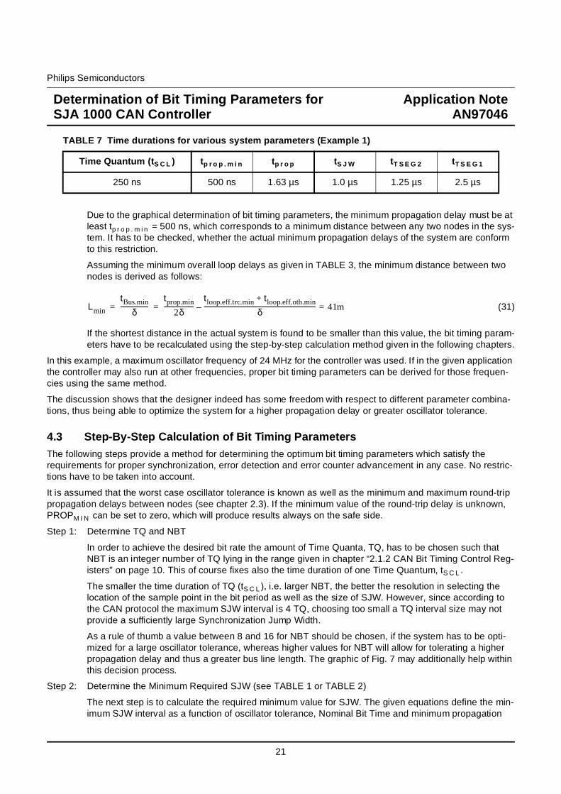
4.2.1 Example 1 . . . . . . . . . . . . . . . . . . . . . . . . . . . . . . . . . . . . . . . . 194.3 Step-By-Step Calculation of Bit Timing Parameters . . . . . . . . . . . . . . . . . . . . . . . . 21
4.3.1 Example 2 . . . . . . . . . . . . . . . . . . . . . . . . . . . . . . . . . . . . . . . . 224.3.2 Example 3 . . . . . . . . . . . . . . . . . . . . . . . . . . . . . . . . . . . . . . . . 23
5. REFERENCES . . . . . . . . . . . . . . . . . . . . . . . . . . . . . . . . . . . . . . . . . . . . . . . 25
APPENDIX . . . . . . . . . . . . . . . . . . . . . . . . . . . . . . . . . . . . . . . . . . . . . . . . . 26
6
Determination of Bit Timing Parameters for SJA 1000 CAN Controller
Philips Semiconductors
Application NoteAN97046
(this page has intentionally been left blank)

Determination of Bit Timing Parameters for SJA 1000 CAN Controller
Philips Semiconductors
7
Application NoteAN97046
1. INTRODUCTIONThe Controller Area Network (CAN) - [1] - is a serial, asynchronous, multi-master communication protocol for connecting electronic control modules, sensors and actuators in automobiles or industrial applications. A feature of the CAN protocol is that the bit rate, the bit sample point and number of samples taken in a bit period are user programmable. This gives the user the freedom to optimize the performance of the network for his given applica-tion. During this optimization process the user has to be aware of the relationship between the bit timing parame-ters, the reference oscillator tolerance and the various signal propagation delays in the system. For example, choosing a later sample point in the bit period results in more tolerance with respect to propagation delay and therefore greater bus length. Conversely, choosing a sample point closer to the midpoint of the bit period will allow a greater oscillator tolerance for each node in the system. It quickly becomes apparent that a large allowa-ble oscillator tolerance and a long bus length are conflicting goals, which can only be met through optimization of the bit timing parameters. This report is intended to support users of the Philips CAN controllers - SJA 1000, PCx82C200 - during this optimization process.
The methods discussed in this report allow a CAN user to determine
• if the CAN bit timing requirements can be met by the system
• the optimum bit timing parameters for a given set of system requirements.
2. OVERVIEW ON CAN BIT TIMING RELATIONSHIPS
2.1 Definitions
2.1.1 Structure of a Bit Period
The definitions of the CAN bit timing parameters used in this report are closely related to those used to program the Philips CAN controllers (see [2], [3] and [4] for further information). These relationships are shown in Fig. 1.
The bit rate - fB i t - of a system characterizes the amount of data bits transmitted per time unit. It is defined as given by Equation (1):
(1)fBit1
tBit-------=
Fig. 1 CAN Bit Time Segments
JK70
2181
.GW
M
tTSEG1 tTSEG2tSYNC_SEG
NBT, t
in 3-Sample Mode only
SamplePoint(s)
Bit

8
Determination of Bit Timing Parameters for SJA 1000 CAN Controller
Philips Semiconductors
Application NoteAN97046
The Nominal Bit Time consists of the three non-overlapping segments SYNC_SEG, TSEG1 and TSEG2 with the corresponding time durations tS Y N C _ S E G , tT S E G 1 and tT S E G 2 . Mathematically, the time duration of the Nominal Bit Time, tB i t , is simply the sum of the segment durations:
(2)
Each of these segments is specified as an integer number of the basic unit of time in a bit period, the so called Time Quantum (TQ). The time duration of a Time Quantum is one period of the CAN system clock, tS C L , which is derived from the oscillator reference, tC L K , (see Fig. 2). The CAN system clock can be adjusted by the user via a programmable prescaler (Baud Rate Prescaler, BRP) as given by Equation (3):
(3)
Another time segment of importance to CAN bit timing calculations is the Synchronization Jump Width (SJW), with time duration tS J W . The SJW segment is not a segment of the bit period but rather defines the maximum number of TQ by which a bit period can be lengthened or shortened in the event of resynchronization.
Moreover, the CAN protocol allows the user to specify the bit sample mode (SAM) as either single sample or three sample mode (2 out of 3 voting). In single sample mode, the sample is taken at the end of the TSEG1 inter-val. In three sample mode, two additional samples are taken, spaced one TQ apart and just prior to the end of the TSEG1 interval, as shown in Fig. 1 and Fig. 2.
The bit timing calculations in this report are expressed in terms of the bit time segments, normalized to the period of the CAN system clock (SYNC_SEG, TSEG1, TSEG2, SJW and NBT), which makes the calculations inde-pendent of a specific bit rate. For details see Equations (7) to (11) of the next section.
tBit tSYNC_SEG tTSEG1 tTSEG2+ +=
tSCL BRP 2⋅ tCLK2 BRPfCLK
----------------==
Fig. 2 Principle of deriving the bit period as implemented in Philips CAN controllers
Note: tSCL is the time duration of one Time Quantum (TQ)
oscillator
CANbit period
JK702201.GWM
t
Baud Rate Prescaler (BRP)
TSEG1 TSEG2
sample point(s)SYNC_SEG
(user definable)
(user definable) (user definable)
(fixed)
t Bit
t CLK
t SCL
system clockCAN

Determination of Bit Timing Parameters for SJA 1000 CAN Controller
Philips Semiconductors
9
Application NoteAN97046
2.1.2 CAN Bit Timing Control Registers
As mentioned before, most elements of the bit timing are user definable. Fig. 3 shows the control registers used by all Philips CAN controllers for setting up these bit timing parameters. Obviously, only integer values can be used for the programming of these parameters.
The meaning of the different bits of the control registers is as follows [2], [3], [4], [5]:
BRP: Baud Rate Prescaler Register BTR0 Range: 1....64
(4)
SAM: Sample Mode Register BTR1
(5)
(6)
SJW: Synchronization Jump Width Register BTR0 Range: 1....4
(7)
SYNC_SEG: Synchronization Segment fixed Value: 1
(8)
TSEG1: Bit Time Segment 1 Register BTR1 Range: 1....16
(9)
MSB LSB
BTR0:
MSB LSB
SJWMSB LSB
BRP
SJW.1 SJW.0 BRP.5 BRP.4 BRP.3 BRP.2 BRP.1 BRP.0
JK702202.GWM
MSB LSB
BTR1:
MSB LSB MSB LSB
SAM TSEG2 TSEG1
SAM TSEG2.2 TSEG2.1 TSEG2.0 TSEG1.3 TSEG1.2 TSEG1.1 TSEG1.0
Fig. 3 Structure of bit timing control registers
BRP 32 BRP.5 16 BRP.4 8 BRP.3 4 BRP.3 2 BRP.1 BRP.0 1+ + + + + +=
SAM 0: 1-Sample Mode =
SAM 1: 3-Sample Mode =
SJWtSJW
tSCL------------ 2 SJW.1 SJW.0 1+ += =
SYNC_SEGtSYNC_SEG
tSCL-------------------------- 1= =
TSEG1tTSEG1
tSCL------------------ 8 TSEG1.3 4 TSEG1.2 2 TSEG1.1 TSEG1.0 1+ + + += =

10
Determination of Bit Timing Parameters for SJA 1000 CAN Controller
Philips Semiconductors
Application NoteAN97046
The relationship between these normalized segment values and Nominal Bit Time (NBT) is as follows:
Although NBT is programmable in the range between 3 to 25 TQ, the minimum functional value is 4 TQ in case of 1-Sample Mode and 5 TQ if the 3-Sample Mode is selected.
2.2 Oscillator ToleranceAs explained above, each node in a CAN network derives its bit timing from its own oscillator reference. In real systems, the oscillator reference frequency, fC L K , will deviate from its nominal value due to initial tolerance off-set, aging and ambient temperature variations. The sum of these deviations result in a total oscillator tolerance, defined as ∆f. This oscillator tolerance is a relative tolerance which represents the deviation of the oscillator refer-ence frequency, normalized to the nominal frequency:
(12)
As the CAN system clock is derived directly from the oscillator reference frequency, ∆f represents also the rela-tive tolerance of the system clock. Thus the minimum and maximum values for the period of the system clock can be approximated as follows:
(13)
(14)
The approximations expressed by Equations (13) and (14) are valid assuming a value of ∆f <<1. Clock refer-ences typically used in real systems, such as crystal oscillators (∆f <0.1%), Phase Locked Loop derived frequen-cies (∆f <0.5%) and ceramic resonators (∆f <1.2%) satisfy this assumption.
2.3 Propagation DelayThe significance of propagation delay in a CAN system stems from the fact that CAN allows for non-destructive arbitration between nodes contending for access to the network, as well as in-frame acknowledgement. Arbitra-tion occurs during the identifier field and implies that multiple nodes simultaneously drive their identifier bits onto the bus. As nodes synchronize on bit edges, excessive propagation delay in the system results in invalid arbitra-tion. Ultimately the various delays in the CAN system limit the maximum network bus length at a given bit rate. The one way propagation delay between two nodes A and B, defined as tp r o p ( A , B ) , is shown in Fig. 4. This delay
TSEG2: Bit Time Segment 2 Register BTR1 Range: 1....8
(10)
NOTE: TSEG2 must be chosen≥2 in 1-Sample Mode and≥3 in 3-Sample Mode.
NBT: Nominal Bit Time Range: 3....25
(11)
TSEG2tTSEG2
tSCL------------------ 4 TSEG2.2 2 TSEG2.1 TSEG2.0 1+ + += =
NBTtBit
tSCL---------- SYNC_SEG= TSEG1 TSEG2+ +=
∆ffCLK.max/min fCLK.nom–
fCLK.nom---------------------------------------------------------=
tSCLmin
tSCL.nom
1 ∆f+-------------------- tSCL.nom≈ 1 ∆f–( )⋅=
tSCLmax
tSCL.nom
1 ∆– f-------------------- tSCL.nom≈ 1 ∆f+( )⋅=

Determination of Bit Timing Parameters for SJA 1000 CAN Controller
Philips Semiconductors
11
Application NoteAN97046
is the sum of all the device delays in the signal path, including the transceiver, the CAN controller and the bus medium [8].
Normally, an effective maximum loop delay, tl o o p . e f f , is specified in the data sheets of controllers and transceiv-ers. As an example, according to Fig. 5, the effective loop delay of a transceiver calculates as follows:
Fig. 4 Propagation delay between nodes
JK702183.GWMtprop(A,B)
Bit m of Node A
Bit m of Node B
Node A
Node B
tPprop(B,A)
Sample Point
Fig. 5 Determination of the Round-Trip Delay in a CAN Bus System
TX-Channel
TX-Channel RX-Channel
RX-Channel
TX-Channel RX-Channel
TX-Channel RX-Channel
tLogic tLogictLogictLogic
tRXtTXtRXtTX
Node A Node B
Transmission Medium Transmission Medium
JK70
2182
.GW
M

12
Determination of Bit Timing Parameters for SJA 1000 CAN Controller
Philips Semiconductors
Application NoteAN97046
(15)
As nodes must receive each other’s waveforms, synchronize to them and then transmit back during arbitration, the total propagation delay in the system is the sum of the two nodes’ delays. Assuming that each node in a given network has comparable delays, the total round-trip delay, defined as tp r o p , can be expressed as follows:
(16)
where is the sum of the effective loop delays of all devices but the transceivers in the signal path.
This total round-trip delay is an important factor in calculating the bit timing parameters. As it is application spe-cific, it must be determined individually with respect to specific system constraints.
For the bit timing calculations proposed in this report, the normalized propagation delay is required as defined by Equation (17):
(17)
As this normalized propagation delay is not a programmable controller interval, it is not constrained to be an inte-ger value.
2.4 SynchronizationSynchronization as defined in the CAN Bus Specification guarantees that messages are properly decoded despite phase errors which may accumulate between nodes. These phase errors may occur due to oscillator drift, propagation delays between nodes spatially distributed on the network, or phase errors caused by noise disturbances. Two types of synchronization are defined; hard synchronization and resynchronization.
Hard synchronization only is performed at the beginning of a message frame. After an idle period, every CAN controller on the network initializes its current bit period timing at the first received recessive to dominant edge with SYNC_SEG. Resynchronization is subsequently performed once per each received recessive to dominant edge throughout the remainder of the message.
If such an edge is received during TSEG1, i.e. after SYNC_SEG but before the sample point of the receiver, it is interpreted by the receiver as a late edge sent by a slower transmitter. The TSEG1 segment of the receiver is therefore lengthened to better match the timing of the transmitter. Conversely, if the edge is received after the sample point but before the SYNC_SEG of the receiver, i.e. during TSEG2, the receiver interprets this edge as an early edge from the next bit period sent by a faster transmitter. In this case, the receiver shortens its TSEG2 interval to better match the timing of the faster transmitter. The maximum number of TQ by which a bit interval may be lengthened or shortened during resynchronization is specified by the programmed value of SJW.
As all the segments within the CAN bit period are quantized, i.e. consist of an integer number of TQ, resynchroni-zation only occurs if the absolute phase error is greater than one TQ. Consequently, even between two nodes on the network with exactly the same oscillator reference frequency, there is an uncertainty of one TQ in synchroni-zation, as shown in Fig. 6.
3. DEFINITION OF BIT TIMING REQUIREMENTSA minimum requirement for a CAN system is that two nodes, with each having an oscillator reference at the opposite extreme of the specified frequency tolerance, and with each at opposite ends of the network with the maximum propagation delay between them, must be able to correctly receive and decode every message trans-mitted on the network. In the absence of noise disturbances, the principle of bit stuffing guarantees no more than 10 bit periods between resynchronization edges (i.e. 5 dominant bits followed by 5 recessive bits). This repre-
tloop.eff.trc tTX tRX+=
tprop tprop(A,B) tprop(B,A)+ 2 tBus tloop.eff.trc tloop.eff.oth+ +( )= =
tloop.eff.oth
PROPtprop
tSCL----------=

Determination of Bit Timing Parameters for SJA 1000 CAN Controller
Philips Semiconductors
13
Application NoteAN97046
sents the worst case condition for accumulated phase error during normal communication. This phase error has to be compensated by the programmed Synchronization Jump Width (SJW) and defines the conditions for the minimum value of SJW.
Real systems typically operate in the presence of noise. Noise disturbances can induce CAN error modes which result in more than 10 bit periods between resynchronization edges. In these cases, the requirements for all bits to be properly sampled are more severe due to the longer time between synchronization edges. Failures to prop-erly sample bits in these cases result in improper error detection and error confinement as defined in the CAN protocol. This limits the values, which can be selected for the bit time segment TSEG2.
3.1 Calculation RulesThe calculation of bit timing parameters has already been discussed in several papers, e.g. [6], [7], and results are therefore taken over without further discussion. The sets of equations are summarized in TABLE 1 (1 sample mode) and TABLE 2 (3 sample mode). By means of these formulas, the bit timing parameters SJW and TSEG2 are calculated in dependence of a known Nominal Bit Time and the propagation delay of the system. Afterwards, TSEG1 can be calculated using Equation (11) on page 10. The constraints with respect to the pro-grammability of the parameters are described in chapter “CAN Bit Timing Control Registers” on page 9.
When calculating the required minimum value for SJW according to TABLE 1 or TABLE 2, normally two different values will result. The larger of the two values has to be taken to guarantee both equations are satisfied. It has to be rounded up to the next integer. Conversely, when calculating the allowed maximum value for TSEG2, the smaller of the two values has to be taken to guarantee both equations are satisfied. This smaller value has to be rounded down to the next integer.
Fig. 6 Clock Skew Between Asynchronous Nodes
JK702184.GWMtSCL
tprop(A,B)
Receiver B
within these twopositions Receiver Bis synchronized toTransmitter A
Transmitter A TQ
SYNC_SEG
a)
b)

14
Determination of Bit Timing Parameters for SJA 1000 CAN Controller
Philips Semiconductors
Application NoteAN97046
1. Has to be rounded up to next integer value.2. Has to be rounded down to next inter value.
1. Has to be rounded up to next integer value.2. Has to be rounded down to next inter value.
TABLE 1 Minimum and Maximum Values for SJW and TSEG2 in 1-Sample Mode
Minimum Value 1 Maximum Value 2
SJW
MAX {
, (18)
} (19)
4
TSEG2 MAX { } (20)
MIN { 8 ,
, (21)
} (22)
TABLE 2 Minimum and Maximum Values for SJW and TSEG2 in 3-Sample Mode
minimum value 1 maximum value 2
SJW
MAX {
, (23)
} (24)
4
TSEG2 MAX { } (25)
MIN { 8 ,
, (26)
} (27)
20 NBT f∆⋅ ⋅1 f∆–
---------------------------------
20 NBT⋅ f∆⋅ 1 f∆– PROPMIN–+
1 f∆+---------------------------------------------------------------------------------------
2 SJW,
NBT 1 25 f∆⋅–( ) PROPMAX–
1 f∆–-------------------------------------------------------------------------
NBT 1 25– f∆⋅( ) PROPMAX– 1( f )∆––PROPMIN
2---------------------------+
1 f∆–--------------------------------------------------------------------------------------------------------------------------------
20 NBT f∆⋅ ⋅1 f∆–
---------------------------------
20 NBT f∆⋅⋅ 1 f∆– PROPMIN–+
1 f∆+---------------------------------------------------------------------------------------
3 SJW,
NBT 1( 25 f )∆⋅ PROPMAX–– 2 1( f )∆––
1 f∆–---------------------------------------------------------------------------------------------------------
NBT 1 25 f∆⋅–( ) PROPMAX– 3 1( f )∆––PROPMIN
2---------------------------+
1 f∆–----------------------------------------------------------------------------------------------------------------------------------------

Determination of Bit Timing Parameters for SJA 1000 CAN Controller
Philips Semiconductors
15
Application NoteAN97046
3.2 Graphic Representations of the Calculation RulesUpon starting the development of a CAN based system it is important to specify
• the bit rate, which determines the amount of data transmitted in a certain time, and
• the propagation delay, which determines the maximum bus line length between any two nodes of the system.
Another important decision is where to place the sample point in the bit period. A late sample point will give more tolerance with respect to propagation delay and therefore a longer bus line length. Conversely, choosing an ear-lier sample point will allow for greater oscillator tolerances. The diagrams of Fig. 7 and Fig. 8 are created to give an indication, if the requested system parameters fulfil the requirements for proper CAN bus operation. Further-more, these diagrams can also be used for the determination of proper bit timing parameters.
3.2.1 Definitions and Restrictions
The diagrams described in this chapter are valid under the following constraints:
1. 1 sample mode is used
2. PROPM I N ≥ 2
3. TSEG2M I N = SJWM I N (Fig. 8 only)
If these assumptions don‘t apply, the formulas from TABLE 1 and TABLE 2 must be directly used as described in chapter 4.3.
3.2.2 Determination of the Maximum Bit Rate
Obviously a high bit rate can only be achieved in case of a small system propagation delay. This chapter deals with the relation between bit rate and propagation delay and how to achieve a maximum propagation delay at the required bit rate.
The maximum bit rate of a system is determined by the minimum time duration of the Nominal Bit Time. Using Equations (1), (3) and (11) the maximum bit rate can be calculated as follows:
(28)
Thus in order to achieve a maximum bit rate, the smallest possible value for the Baud Rate Prescaler, BRP, the maximum possible oscillator frequency for the CAN controller, fCLK.max, and the minimum value for the bit time segments, expressed by NBT, have to be selected.
The minimum Nominal Bit Time can be determined using Equation (21),
, (29)
which is valid if PROPM I N ≥ 2. This relation between the maximum propagation delay and the minimum Nominal Bit Time is visualized in Fig. 7. The oscillator tolerance is the dominating parameter in this graph. But due to implementation specific constraints, the amount of Time Quanta of each normalized bit time segment is restricted to certain integer values. These additionally have been taken into account for the creation of Fig. 7 (compare with Equations (7), (8), (9) and (10)). Furthermore, the diagram includes a list of the maximum values for NBT to be obtained at the different oscillator tolerances. These values have been calculated using Equation (18) together with the constraint SJW ≤4, and considering the maximum programmable value for NBT. Note that NBT is an integer value, whereas PROPM A X is not constrained to be an integer.
Bit Ratemax1
tSCL.min NBTmin⋅-------------------------------------------=
fCLK.max
2 BRPmin NBTmin⋅ ⋅--------------------------------------------------=
NBTPROPMAX TSEG2+ 1(⋅ f )∆–
1 25 f∆⋅–---------------------------------------------------------------------------≥

16
Determination of Bit Timing Parameters for SJA 1000 CAN Controller
Philips Semiconductors
Application NoteAN97046
Consequently, Fig. 7 can be used to determine if the requested maximum bit rate and propagation delay of a sys-
tem do match, i.e. whether such a system configuration can be implemented or not. This procedure is explained in detail while discussing the examples of chapter 4. The general procedure is as follows:
First the required product of BRP and NBT has to be calculated with respect to bit rate and oscillator frequency by using Equation (28). This product has to be an integer value. Normally, different combinations of BRP and NBT will be possible resulting in different time durations for one Time Quanta. The physical duration of one Time Quanta can be calculated using Equation (3). The possible NBT values are then used to determine PROPM A X from Fig. 7. Afterwards, Equation (17) gives the maximum propagation delay tolerated by the system. This value has to be higher than the actual propagation delay in the system.
3.2.3 Determination of a Proper Sample Point
The position of the sample point in a bit time is fully determined by TSEG2 (compare Fig. 2 on page 8). The cal-culation rules given in TABLE 1 and TABLE 2 define a minimum and a maximum value for TSEG2, which depend on the Nominal Bit Time and the propagation delay in the system. Consequently, if the position of the sample point is expressed as a percentage of the bit time, a diagram can be constructed, where the sample point merely depends on the maximum propagation delay and the oscillator tolerance. Such an diagram is given in Fig. 8. The relationship used for the construction is defined by the following equation:
(30)
Fig. 7 Determination of minimum Nominal Bit Time (maximum Bit Rate) - 1-Sample Mode only
0
5
10
15
20
25
2 3 4 5 6 7 8 9 10 11 12 13 14 15 16Maximum Propagation Delay [TQ]
Min
imum
Nom
inal
Bit
Tim
e [T
Q]
JK70
7082
.GW
M/B
ITR
AT
E5.
XLS
(DIA
1)
∆f = 0,1%
∆f = 0,5%∆f = 1,0%
∆f = 1,5%
max values for NBT∆f = 0,1% : 25∆f = 0,5% : 25∆f = 1,0% : 19∆f = 1,5% : 13
Tsample_pointNBT TSEG2–
NBT--------------------------------------- 100%⋅=

Determination of Bit Timing Parameters for SJA 1000 CAN Controller
Philips Semiconductors
17
Application NoteAN97046
The shaded regions of Fig. 8 represent the allowed range for the sample point at a given propagation delay and a given oscillator tolerance. As mentioned before, the diagram is valid only under the restrictions described in chapter 3.2.1.
Fig. 8 may be used to derive the range for a proper sample point position for a certain requested maximum prop-agation delay also expressed in percent of the bit time period. For example, assuming an oscillator tolerance of 0.5% and a maximum propagation delay of 62,5% of the bit period as indicated for case b, the sample point posi-tion has to be in the range between 75% and 90% of the bit time. With the help of Equation (30), the correspond-ing range for TSEG2 can be calculated.
As further can be seen from Fig. 8, the maximum propagation delay to be achieved with an oscillator tolerance of 0.5% is 77% of a bit time (see case a) with a sample point at exactly 90% of a bit time period. For this exact sam-ple point position it is not expected that TSEG2 is an integer value in any case. As a consequence, these extremes can normally not be implemented and are therefore theoretical values.
4. CALCULATION OF BIT TIMING PARAMETERSIn real applications certain, normally contrary requirements have to be met to get the necessary system perform-ance.
These requirements may be
• a high data throughput, i.e. the bit rate is affected
• a long bus length, i.e. the propagation delay is affected
• a small system price, which may affect the oscillator tolerance; e.g. by selecting ceramic resonators instead of crystal oscillators
Fig. 8 Diagram for deriving a proper sample point position (1-Sample Mode only)
������������������������������������������������������������������������������������������������������������������������������������������������������������������������������������������������������������������������������������������������������������������������������������������������������������������������������������������������������������������������������������������������������������������������������������������������������������������������������������������������������������������������������������������������������������������������������������������������������������������������������������������������������������������������������������������������������������������������������������������������������������������������������������������������������������������������������������������������������������������������������������������������������������������������������������������������������������������������������������������������������������������������������������������������������������������������������������������������������������������������������������������������������������������������������������������������������������������������������������������������������������������������������������������������������������������������������������������������������������������������������������������������������������������������������������������������������������������������������������������������������������������������������������������������������������������������������������������������������������������������������������������������������������������������������������������������������������������������������������������������������������������������������������������������������������������������������������������������������������������������������������������������������������������������������������������������������������������������������������������������������������������������������������������������������������������������������������������������������������������������������������������������������������������������������������������������������������������������������������������������������������������������������������������������������������������������������������������������������������������������������������������������������������������������������������������������������������������������������������������������������������������������������������������������������������������������������������������������������������������������������������������������������������������������������������������������������������������������������������������������������������������������
������������������������������������������������������������������������������������������������������������������������������������������������������������������������������������������������������������������������������������������������������������������������������������������������������������������������������������������������������������������������������������������������������������������������������������������������������������������������������������������������������������������������������������������������������������������������������������������������������������������������������������������������������������������������������������������������������������������������������������������������������������������������������������������������������������������������������������������������������������������������������������������������������������������������������������������������������������������������������������������������������������������������������������������������������������������������������������������������������������������������������������������������������������������������������������������������������������������������������������������������������������������������������������������������������������������������������������������������������������������������������������������������������������������������������������������������������������������������������������������������������������������������������������������������������������������������������������������������������������������������������������������������������������������������������������������������������������������������������������������������������������������������������������������������������������������������������������������
��������������������������������������������������������������������������������������������������������������������������������������������������������������������������������������������������������������������������������������������������������������������������������������������������������������������������������������������������������������������������������������������������������������������������������������������������������������������������������������������������������������������������������������������������������������������������������������������������������������������������������������������������������������������������������������������������������������������������������������������������������������������������������������������������������������������������������������������������������������������������������������������������������������������������������������
�������������������������������������������������������������������������������������������������������������������������������������������������������������������������������������������������������������������������������������������������������������������������������������������������������������������������������������
����
����
��
Case b ���������������������� Case a
JK70
7081
.GW
M
10
20
30 40
50
60
70
80
90
100
10
20
30
40
50
60
70 80 90
100
����������
��������
Maximum Propagation Delay[% of Bit Time]
Pos
ition
of t
he S
amp
le P
oin
t[%
of B
it T
ime]

18
Determination of Bit Timing Parameters for SJA 1000 CAN Controller
Philips Semiconductors
Application NoteAN97046
This chapter shows, how to derive the optimum bit timing parameters for a given set of system requirements, using either the diagrams of Fig. 7 and Fig. 8 or the calculation rules defined in TABLE 1 and TABLE 2.
4.1 Example DefinitionAll examples used in this chapter are built around the set of system parameters given in TABLE 3.
4.2 Selecting Bit Timing Parameters Using the Graphic RepresentationThis chapter describes a step-by-step method for deriving optimum bit timing parameters when using Fig. 7 and Fig. 8. It is assumed that the oscillator frequency, the requested bit rate, the worst case oscillator tolerance and the minimum and maximum round-trip propagation delays between any two nodes of the system are known. As for the graphical representation the minimum propagation delay is restricted to 2 Time Quanta, it has to be checked in any case, whether the actual minimum system propagation delay is not below this limit. The proce-dure of determining proper bit timing parameters is as follows:
Step 1: Determine BRP, NBT, the duration of a Time Quantum, tS C L , and PROP
Using Equation (28) the product of BRP and NBT can be calculated in dependence of the required bit rate and oscillator frequency. This product has to be an integer value. In general, the usage of several different combinations of BRP and NBT might be possible. All combinations should be written down in a list or table. Afterwards, the corresponding Time Quanta time durations have to be calculated using Equation (3) and added to the list.
Furthermore, the maximum and minimum round-trip delays have to be determined by using Equation (16). The propagation delay is composed of the effective loop delays of all components involved, addi-tionally adding the line delay between the farthest ends of the bus lines in the system, as indicated in
1. Minimum values for the controllers and transceivers are assumptions only.
TABLE 3 Requirements for a CAN Bus System
Parameter Explanation Minimum 1 Nominal Maximum
fB i t Bit Rate 250 kBit/s
tB i t time duration of the Nominal Bit Time 4 µs
fC L K oscillator frequency of the CAN controller e.g SJA 1000 24 MHz
oscillator tolerance 1.0%
effective loop delay of a transceiver e.g. PCA82C251 30 ns 75 ns 157 ns
loop delay of the logic e.g. of a controller SJA 1000 15 ns 40 ns
specific line delay 5 ns/m 6.5 ns/m
L bus line length between nodes 3 m 95 m
tB u s calculated bus line delay: 15 ns 618 ns
tp r o p calculated propagation delay:
120 ns1630 ns
(≈41% of tB i t )
f∆
tloop.eff.trc
t loop.eff.oth
δ
tBus L δ⋅=
tprop 2 tloop.eff.trc tloop.eff.oth tBus+ +( )⋅=

Determination of Bit Timing Parameters for SJA 1000 CAN Controller
Philips Semiconductors
19
Application NoteAN97046
Fig. 5 on page 11. With the known time duration, the normalized value, PROP, is calculated using Equation (17). This calculations have to be performed for each derived tS C L value.
Step 2: Select proper combinations of NBT, PROP and BRP
The derived combinations of NBT and PROP are now compared with the minimum and maximum val-ues for NBT given in Fig. 7. All combinations should be marked to be valid or not.
Step 3: Judge the trade-off between bit rate and propagation delay
One combination of BRP, NBT, PROP and oscillator tolerance has to be selected for continuing with the next step. If the selection of NBT or PROP leaves room for further enhancements of the system, e.g. higher bit rates or larger propagation delay, it has to be decided which parameter should be opti-mized.
Step 4: Select a proper sample point position and calculate the bit timing parameters
After having confirmed that a proper combination of BRP and NBT does exist, Fig. 8 can be used to determine the bit timing parameters. With the knowledge of the maximum propagation delay and the value for the bit time period, a proper sample point position range can be derived from this diagram. Having once determined this range, the minimum and maximum value for the bit time segment TSEG2 can be calculated using Equation (30). The results have to be rounded up/down to an integer value. Note that TSEG2 must be at least 2 TQ due to implementation constraints. SJW is equal to the mini-mum value of TSEG2 but is not constraint to be at least 2 TQ. Therefore the calculated minimum value for TSEG2 determines the required minimum value for SJW in any case. With known TSEG2 and NBT, TSEG1 is calculated according to Equation (11). The resulting values may be used for programming the bit timing control registers of the CAN controller.
Step 5: Check the PROPM I N restriction
After having derived the full set of bit timing parameters, it has to be checked whether the minimum propagation delay in the system is greater than 2 TQ as assumed. If this restriction does not apply, the bit timing parameters should be recalculated using the formulas from TABLE 1 in order to verify the chosen bit timing (see also chapter 4.3).
4.2.1 Example 1
For this example a system as defined in TABLE 3 is assumed. The example is intended to clarify the determina-tion of bit timing parameters using the graphic representation of the calculation rules. As in this method a mini-mum propagation delay of more than 2 TQ is assumed, the minimum values for the propagation delay additionally given in TABLE 3 are not taken into account in the first steps of calculation.
Step 1: Determine BRP, NBT, the duration of a Time Quantum, tS C L , and PROP
For the given oscillator frequency of 24 MHz, the product of BRP and NBT is 48. The different possible combinations of BRP and NBT are listed in TABLE 4, together with the calculated values for the time duration of one Time Quantum and the normalized values of the propagation delay, PROP.
Step 2: Select proper combinations of NBT, PROP and BRP
The results are given in TABLE 4. The two extreme combinations are invalid.
Step 3: Judge the trade-off between bit rate and propagation delay
The parameters giving NBT = 16 are selected, as they result in the minimum value for the Time Quan-tum and thus leaving most freedom for selecting a proper sample point position in the following step.
Step 4: Select a proper sample point position and calculate the bit timing parameters
According to Fig. 8, a proper sample point can be chosen between 65% and 80% of the Nominal Bit Time ( , PROP = 41% of the bit time period). This gives the following constraints for TSEG2 f∆ 1.0%=

20
Determination of Bit Timing Parameters for SJA 1000 CAN Controller
Philips Semiconductors
Application NoteAN97046
and SJW:
TSEG2:
SJW:
As a larger value of tT S E G 2 provides for a greater margin for proper sampling in the presence of noise, a value near 65% of the Nominal Bit Time should be chosen for the sample point. For tS J W a value as small as possible has to be chosen to limit the effect of false resynchronization caused by spikes.
Using NBT = 16 (Step 4), SJW = 4 has to be selected and TSEG2 can be chosen between 4 and 5 TQ.The results are summarized in TABLE 5, TABLE 6 and TABLE 7. Here TSEG2 is set to 5 TQ. This cor-responds to a sample point at 69% of the bit time period. According to Fig. 8 this would allow for tolerat-ing a propagation delay of approximately 42%. On the other hand, if TSEG2 would be set to 4 TQ corresponding to a sample point at 75% of a bit time, a propagation delay of approximately 50% could be tolerated.
Step 5: Check the PROPM I N restriction
TABLE 4 Determination of BRP, NBT and PROP for Example 1
calculated using Equations (28) and (3) Compare with Fig. 7 ( )
fC L K BRP NBT t S C L PROP Valid Remark
24 MHz
2 24 166.6 ns 9.78 no NBT exceeds maximum value
3 16 250.0 ns 6.52 yes
4 12 333.3 ns 4.89 yes
6 8 500.0 ns 3.26 yes
8 6 666.6 ns 2.45 yes
12 4 1000 ns 1.63 no NBT too small, PROP <2
TABLE 5 Results Example 1 (normalized values for programming)
fC L K BRP NBT PROP M I N PROP SJW TSEG2 TSEG1
24 MHz 3 16 2 6.524
(≥3.2) 5
(≥3.2;≤5.6)10
TABLE 6 Programming of the control registers of SJA 1000, P Cx82C200 (Example 1)
BTR0[HEX]
SJW BRP BTR1[HEX]
SAM TSEG2 TSEG1
C2 1 1 0 0 0 0 1 0 49 0 1 0 0 1 0 0 1
20% of tBit 800 ns=( ) tTSEG2 35% of tBit 1400 ns=( )< <
tSJW 20% of tBit 800 ns=>
f 1%=∆
Determination of Bit Timing Parameters for SJA 1000 CAN Controller
Philips Semiconductors
21
Application NoteAN97046
Due to the graphical determination of bit timing parameters, the minimum propagation delay must be at least tp r o p . m i n = 500 ns, which corresponds to a minimum distance between any two nodes in the sys-tem. It has to be checked, whether the actual minimum propagation delays of the system are conform to this restriction.
Assuming the minimum overall loop delays as given in TABLE 3, the minimum distance between two nodes is derived as follows:
(31)
If the shortest distance in the actual system is found to be smaller than this value, the bit timing param-eters have to be recalculated using the step-by-step calculation method given in the following chapters.
In this example, a maximum oscillator frequency of 24 MHz for the controller was used. If in the given application the controller may also run at other frequencies, proper bit timing parameters can be derived for those frequen-cies using the same method.
The discussion shows that the designer indeed has some freedom with respect to different parameter combina-tions, thus being able to optimize the system for a higher propagation delay or greater oscillator tolerance.
4.3 Step-By-Step Calculation of Bit Timing ParametersThe following steps provide a method for determining the optimum bit timing parameters which satisfy the requirements for proper synchronization, error detection and error counter advancement in any case. No restric-tions have to be taken into account.
It is assumed that the worst case oscillator tolerance is known as well as the minimum and maximum round-trip propagation delays between nodes (see chapter 2.3). If the minimum value of the round-trip delay is unknown, PROPM I N can be set to zero, which will produce results always on the safe side.
Step 1: Determine TQ and NBT
In order to achieve the desired bit rate the amount of Time Quanta, TQ, has to be chosen such that NBT is an integer number of TQ lying in the range given in chapter “2.1.2 CAN Bit Timing Control Reg-isters” on page 10. This of course fixes also the time duration of one Time Quantum, tS C L .
The smaller the time duration of TQ (tS C L ), i.e. larger NBT, the better the resolution in selecting the location of the sample point in the bit period as well as the size of SJW. However, since according to the CAN protocol the maximum SJW interval is 4 TQ, choosing too small a TQ interval size may not provide a sufficiently large Synchronization Jump Width.
As a rule of thumb a value between 8 and 16 for NBT should be chosen, if the system has to be opti-mized for a large oscillator tolerance, whereas higher values for NBT will allow for tolerating a higher propagation delay and thus a greater bus line length. The graphic of Fig. 7 may additionally help within this decision process.
Step 2: Determine the Minimum Required SJW (see TABLE 1 or TABLE 2)
The next step is to calculate the required minimum value for SJW. The given equations define the min-imum SJW interval as a function of oscillator tolerance, Nominal Bit Time and minimum propagation
TABLE 7 Time durations for various system parameters (Example 1)
Time Quantum (t S C L ) tp r o p . m i n tp r o p tS J W tT S E G 2 tT S E G 1
250 ns 500 ns 1.63 µs 1.0 µs 1.25 µs 2.5 µs
Lmin
tBus.min
δ------------------
tprop.min
2δ-------------------
tloop.eff.trc.min tloop.eff.oth.min+
δ----------------------------------------------------------------------- 41m=–= =

22
Determination of Bit Timing Parameters for SJA 1000 CAN Controller
Philips Semiconductors
Application NoteAN97046
delay. If the minimum propagation delay between any two nodes in the given system may be difficult to determine, a zero value can be selected, which gives a conservative first estimate.
The larger of the two values calculated from the equations must be taken to guarantee both equations are satisfied. The SJW interval has to be an integer number of TQ, so the chosen value must be rounded up to the next integer. If the calculated SJW is greater than 4, the initially fixed TQ interval must be increased (NBT reduced), or a more accurate oscillator type has to be used.
Step 3: Determine the Minimum Value for TSEG2 (see TABLE 1 or TABLE 2)
The minimum allowed size of the TSEG2 interval is determined from the requirement for the CAN con-troller to properly resynchronize together with the minimum requirement for the SJW interval. For proper resynchronization, the TSEG2 interval must be at least 2 TQ, which allows TSEG2 to be short-ened in the event of an early received edge by ensuring a minimum Information Processing time. Fur-thermore, the TSEG2 segment must be as large as the SJW interval determined in Step 2 above. As a result, the minimum TSEG2 interval must be at least as great as the larger of these two constraints.
Step 4: Determine the Maximum Value for TSEG2 (see TABLE 1 or TABLE 2)
As a CAN network is more tolerant to system propagation delay the later the sample point is positioned in the bit period, the maximum system propagation delay limits the maximum allowable TSEG2 interval. Assuming the maximum system propagation delay is known, the TSEG2 upper limit can be calculated from the equations given. With respect to the minimum system propagation delay, if the actual mini-mum propagation delay between any two nodes in the system is not known, the most conservative esti-mate is to assume it is zero.
The smaller of the values calculated from the equations must be taken to guarantee both equations are satisfied. As the TSEG2 interval must be an integer number of TQ, the smaller value must be rounded down to the next integer.
Step 5: Choosing the Correct Bit Timing Parameters
Based on the results of steps 3 and 4, the requirements for minimum and maximum TSEG2 interval size, converted to an integer number of TQ, may allow a range of possible TSEG2 values. The largest possible value which satisfies all the requirements should be chosen, as this provides the greatest mar-gin for proper sampling in the presence of noise. Conversely, SJW has to be chosen as small as possi-ble to limit the effect of false resynchronization caused by spikes.
When TSEG2 has been fixed, TSEG1 is calculated using Equation (11) on page 10. Afterwards, all results have to be checked with respect to the allowed programmable range as given in chapter “2.1.2 CAN Bit Timing Control Registers” on page 9.
If the maximum system propagation delay is so large that the minimum and maximum TSEG2 values are contradictory, the overall system requirements cannot be met as specified. One possible solution is to use a more precise oscillator type. A second possible solution is to reduce the maximum propagation delay by employing other devices or by reconfiguring the devices used. For example, the slope-control function provided by the Philips transceivers PCA82C250 and PCA82C251 influences their delay sig-nificantly [8]. Assuming radiated emissions requirements can be met with faster edge transitions, less slope control may reduce the system propagation delay, enabling a solution to all of the bit timing requirements.
4.3.1 Example 2
Assuming the results from Example 1 were not satisfying with respect to the minimum distance between two nodes evolved from the minimum propagation delay, the bit timing has to be recalculated using the complete set of system parameters given in TABLE 3. The procedure is as follows:

Determination of Bit Timing Parameters for SJA 1000 CAN Controller
Philips Semiconductors
23
Application NoteAN97046
Step 1: Possible values for NBT have already been discussed in Example 1. A commonly used partition is NBT = 16, which implies a Time Quantum time duration of tS C L = 250 ns for the requested Nominal Bit Time of tB i t = 4 µs.
This can be achieved, for example, with a value of BRP = 3 for the prescaler and an oscillator fre-quency of 24 MHz or using BRP = 2 at 16 MHz is used. Other values may also be selected.
Step 2: The minimum values for SJW are calculated using Equations (18) and (19) for the 1-Sample Mode.
In this example, the minimum propagation delay is 120 ns, which corresponds to a normalized value of PROPM I N = 0.48. Both equations give a result above 3 (3.23 and 3.67). Consequently, SJW = 4 has to be chosen.
Step 3: According to Equation (20): TSEG2m i n = 4.
Step 4: The maximum TSEG2 interval size is calculated using Equations (21) and (22).
The maximum propagation delay of 1.63 µs corresponds to a normalized value of PROPM A X = 6.52. As above: PROPM I N = 0.48. The results of both equations (5.54 and 4.78) are rounded down to the next integer value what gives 5 and 4 respectively. Thus the maximum value for TSEG2 has to be set to 4 TQ.
Step 5: The resulting TSEG1 is calculated according to Equation (11).
Because there is no conflict in the calculated minimum and maximum requirement for TSEG2, the bit timing parameter NBT=16, SJW=4, TSEG2=4 and TSEG1=11 satisfy the system requirements and therefore may be programmed..
This example shows that if the actual minimum propagation delay is taken into account, which is smaller than 2 TQ, only one value can be selected for TSEG2. It is the smaller of the two possibilities calculated in Example 1.
TABLE 8 List of values for SJW, TSEG2 and TSEG1 in 1-Sample Mode (Example 2)
calculated values(NBT = 16, PROPM A X = 6.52, PROPM I N = 0.48) selected values
minimum maximum
SJW Maximum of { 3.23 , 3.67 } 4 4
TSEG2 Maximum of { 2 , SJW } Minimum of { 8 , 5.54 , 4.78 } 4
TSEG1 TSEG1 = NBT - TSEG2 - SYNC_SEG 11
TABLE 9 Programming of the control registers of SJA 1000, P Cx82C200 (Example 2)
BTR0[HEX]
SJW BRP(= 3 for f C L K = 24 MHz)
BTR1[HEX]
SAM TSEG2 TSEG1
C2 1 1 0 0 0 0 1 0 3A 0 0 1 1 1 0 1 0
TABLE 10 Time durations for various system parameters (Example 2)
Time Quantum (t S C L ) tp r o p . m i n tp r o p tS J W tT S E G 2 tT S E G 1
250 ns 120 ns 1.63 µs 1.0 µs 1.0 µs 2.75 µs

24
Determination of Bit Timing Parameters for SJA 1000 CAN Controller
Philips Semiconductors
Application NoteAN97046
4.3.2 Example 3
In the previous two examples the 1-Sample Mode was required. If the 3-Sample Mode should be used in order to reduce sampling errors in the presence of noise, the bit timing parameters can be calculated using the formulas from TABLE 2. Assuming the same system requirements as given in TABLE 3, the results are as follows:
Step 1: Taking the partition as used in Example 2 gives:NBT = 16 ==> tS C L = 250 nsBRP = 3 for oscillator frequency of 24 MHz.
Step 2: The minimum values for SJW are calculated using Equations (23) and (24).
With PROPM I N = 0.48, both equations give a rounded up result of 4 TQ. Consequently, SJW = 4 has to be chosen.
Step 3: According to Equation (25): TSEG2m i n = 4.
Step 4: The maximum TSEG2 size is calculated using Equations (26) and (27)
The maximum propagation delay corresponds to a normalized value of 6.52. The results of the equa-tions (3.54 and 2.78) are rounded down to a next integer value giving 3 and 2 respectively. Thus the maximum value for TSEG2 has to be set to 2.
As it becomes clear, there is a conflict between the calculated minimum and maximum values for TSEG2. Thus the system requirements can not be met for 3-Sample Mode .
All results calculated so far are summarized in TABLE 11.
A way out is to recalculate the bit timing parameters while changing the constraints. The following items may be functional in such a case:
1. Reduction of the desired maximum propagation delay.Assuming a maximum propagation delay of at most 1250 ns (normalized value: 5.0) reduces the maximum bus line length to
If this lower performance can also be accepted, a functional alternative has been found. The resulting bittiming parameters are summarized in TABLE 12.
1. conflict between minimum and maximum value
TABLE 11 List of values for SJW, TSEG2, TSEG1 in 3-Sample Mode (Example 3)
calculated values(NBT = 16, PROPM A X = 6.52, PROPM I N = 0.48) selected values
minimum maximum
SJW Maximum of { 3.23 , 3.67 } 4 4
TSEG2 Maximum of { 3, SJW } Minimum of { 8 , 3.54 , 2.78 } ----- 1
TSEG1 TSEG1 = NBT - TSEG2 - SYNC_SEG -----
Lmax
tprop.max
2 δ⋅--------------------
tloop.eff.trc.max tloop.eff.oth.max+
δ------------------------------------------------------------------------– 54 m= =

Determination of Bit Timing Parameters for SJA 1000 CAN Controller
Philips Semiconductors
25
Application NoteAN97046
2. Usage of an oscillator with less toleranceEven if an oscillator with less tolerance can be used, the situation will be much more relaxed. TABLE 13 summarizes the resulting bit timing parameters if an oscillator type with a tolerance of at most is used for the given example.
As it can be seen from the above examples, there should be enough room for individual system optimization. With the methods described in this report, users of the SJA1000 should be able to easily find the optimal bit tim-ing parameters according to their individual requirements.
5. REFERENCES[1] CAN Specification Version 2.0, Parts A and B, Philips Semiconductors, 1992
[2] Philips Semiconductors, Data Sheet SJA 1000, April 1997
[3] Philips Semiconductors, Data Sheet PCx82C200, November 1992
[4] Philips Semiconductors, Data Handbook IC18, Semiconductors for In-car Electronics 1996
[5] Philips Semiconductors, Data Handbook IC20, 80C51-Based 8-bit Microcontrollers 1997
[6] Dietmayer, K.: CAN Bit Timing, Philips Semiconductors, Technical Report HAI/TR9708, 1997
[7] Dietmayer, K.; Overberg, K. W.: CAN Bit Timing Requirements, SAE Paper 970295, 1997
[8] Eisele, H. and Jöhnk, E.: Application Note PCA82C250/251 CAN Transceiver, AN96116, Philips Semicon-ductors, 1996
TABLE 12 List of values for SJW, TSEG2, TSEG1 in 3-Sample Mode (Example 3, Alternative 1.)
calculated values for changed requirements selected values
minimum maximum
SJW Maximum of { 3.23 , 3.67 } 4 4
TSEG2 Maximum of { 3, SJW } Minimum of { 8 , 5.07 , 4.31 } 4
TSEG1 TSEG1 = NBT - TSEG2 - SYNC_SEG 11
TABLE 13 List of Values for SJW, TSEG2, TSEG1 in 3-Sample Mode (Example 3, Alternative 2.)
calculated values for changed requirements selected values
minimum maximum
SJW Maximum of { 1.61 , 2.1 } 4 3
TSEG2 Maximum of { 3, SJW } Minimum of { 8 , 5.52 , 4.76 } 3
TSEG1 TSEG1 = NBT - TSEG2 - SYNC_SEG 12
f∆ 0.5%=

26
Determination of Bit Timing Parameters for SJA 1000 CAN Controller
Philips Semiconductors
Application NoteAN97046
APPENDIX
A List of Used Indices and Variables
A.1 Indices
Bit corresponds to the bit period
CLK corresponds to oscillator reference clock
max used for indication of maximum values
min used for indication of minimum values
nom used for indication of nominal values
SLC corresponds to the CAN system clock which is derived from the oscillator reference
A.2 Variables
δ [s/m] specific line delay per length unit (e.g. 5 ns/m)
f [Hz] frequency
L [m] length of the bus wires between two bus nodes
t [s] fixed point in time, time duration
tB u s [s] delay of the bus or transfer medium, respectively
tloop.eff . trc [s] effective transceiver loop delay between pin TxD (transmit data input) and RxD (receive data output)
tloop.eff .o th [s] effective loop delay of other components in the transmission path e.g. CAN controller output/input logic
tprop [s] round-trip delay or two-way propagation delay (limited by CAN bit timing parameters)
tSJW [s] time duration of the Synchronization Jump Width
tS Y N C _ S E G [s] time duration of the Synchronization Segment
tT S E G 1 [s] time duration of the Bit Time Segment 1
tT S E G 2 [s] time duration of the Bit Time Segment 2
tP R O P _ S E G [s] time duration of the Propagation Segment
BRP [1] Baud Rate Prescaler for generating the CAN system clock
NBT [1] normalized duration of the Nominal Bit Time
PROP [1] normalized round-trip delay or two-way propagation delay
SJW [1] normalized duration of the Synchronization Jump Width
SYNC_SEG [1] normalized duration of the Synchronization Segment
TQ [1] Time Quantum, basic unit of time in a bit period
TSEG1 [1] normalized duration of the Bit Time Segment 1
TSEG2 [1] normalized duration of the Bit Time Segment 2
PROP [1] normalized round-trip delay or two-way propagation delay