development and benchmarking of new hardware …
TRANSCRIPT

DEVELOPMENT AND BENCHMARKING OF NEW HARDWAREARCHITECTURES FOR EMERGING CRYPTOGRAPHIC TRANSFORMATIONS
by
Marcin RogawskiA Dissertation
Submitted to theGraduate Faculty
ofGeorge Mason UniversityIn Partial fulfillment of
The Requirements for the Degreeof
Doctor of PhilosophyElectrical and Computer Engineering
Committee:
Dr. Kris Gaj, Dissertation Director
Dr. Jens-Peter Kaps, Committee Member
Dr. Qiliang Li, Committee Member
Dr. Massimiliano Albanese, Committee Member
Dr. Andre Manitius, Department Chair
Dr. Kenneth S. Ball, Dean, Volgenau Schoolof Engineering
Date: Summer Semester 2013George Mason UniversityFairfax, VA

Development and Benchmarking of New Hardware Architectures for EmergingCryptographic Transformations
A dissertation submitted in partial fulfillment of the requirements for the degree ofDoctor of Philosophy at George Mason University
By
Marcin RogawskiMaster of Science
Military University of Technology, 2003
Director: Dr. Kris Gaj, Associate ProfessorDepartment of Electrical and Computer Engineering
Summer Semester 2013George Mason University
Fairfax, VA

Copyright © 2013 by Marcin RogawskiAll Rights Reserved
ii

Dedication
I dedicate this dissertation to my beloved wife and constant advocate, Kasia. Her patience,trust and support during these years in withstanding all the hours lost to my studies wascritical to my success. To my mother Danusia and my stepfather Bohdan, who gave me thecharacter and goal-oriented attitude, which has enabled me to get this far. To my parents-in-law Jadwiga and Czes law, who always believe, that my crazy ideas will work. Finally, Idedicate this thesis to the memory of my father Stanis law.
iii

Acknowledgments
This research was partially supported by National Institute of Standards and Tech-nology through the Recovery Act Measurement Science and Engineering Research GrantProgram, under contract no. 60NANB10D004 (Project title: Environment for Fair andComprehensive Performance Evaluation of Cryptographic Hardware and Software).
It is my great pleasure, but also a must, to acknowledge multiple individuals who sup-ported me directly or indirectly in closing successfully this important chapter of my life.
First of all, I want to thank my advisor, Prof. Kris Gaj. I owe a lot to him for his preciousguidance, support, encouragement, and always friendly atmosphere. His open mind, broadspectrum of knowledge, and accurate thinking helped me accomplish my goals. He has beena great mentor as well as a source of inspiration throughout my PhD study.
Furthermore, I like to thank Prof. Jens-Peter Kaps for his very valuable time, remarks,and comments. All of them were always delivered in a very constructive, but also cheerfulform.
I also thank other dissertation committee members, Prof. Qiliang Li and Prof. Mas-similiano Albanese. They provided sustained guidance, comments, advice and made mydefense in almost relaxed atmosphere.
I would like to thank Prof. Andre Manitius for everything he has done for me an mywife. He made my GMU study time almost stress-free!
The role of supportive and welcoming friends and colleagues in the life of a researcher cannot be forgotten. I would like to thank all the present and former members of CryptographicEngineering Research Group, with a special distinction for Ekawat Homsirikamol for ourmodel cooperation.
Finally, I would like to thank my wife, my parents, my brothers, and my big family fortheir unconditional support and for taking care of me more than I sometimes deserved.
iv

Table of Contents
Page
List of Tables . . . . . . . . . . . . . . . . . . . . . . . . . . . . . . . . . . . . . . . . viii
List of Figures . . . . . . . . . . . . . . . . . . . . . . . . . . . . . . . . . . . . . . . . x
Abstract . . . . . . . . . . . . . . . . . . . . . . . . . . . . . . . . . . . . . . . . . . . xii
1 Introduction . . . . . . . . . . . . . . . . . . . . . . . . . . . . . . . . . . . . . . 0
1.1 Motivation . . . . . . . . . . . . . . . . . . . . . . . . . . . . . . . . . . . . 0
1.2 Summary of research contributions . . . . . . . . . . . . . . . . . . . . . . . 7
1.2.1 Novel hardware accelerator for authenticated encryption . . . . . . . 7
1.2.2 An adaptation of the T-box method to the AES-like hash functions 8
1.2.3 A novel, adder/subtractor for thousand bit and more using fast carry
chains of modern FPGAs . . . . . . . . . . . . . . . . . . . . . . . . 9
1.2.4 New approach to arithmetic based on the Solinas primes for Pairing-
based Cryptography . . . . . . . . . . . . . . . . . . . . . . . . . . . 9
1.2.5 Novel hardware architectures for pairing on Edwards curves . . . . . 10
1.2.6 A heuristic strategy for FPGA-oriented electronic design automation 11
I High-performance hardware architectures supporting confidentiality
and integrity 13
2 High-Throughput hardware architectures of AES-like Cryptographic hash functions 14
2.1 Introduction and motivation . . . . . . . . . . . . . . . . . . . . . . . . . . . 14
2.2 Previous work . . . . . . . . . . . . . . . . . . . . . . . . . . . . . . . . . . . 17
2.2.1 Grøstl in SHA-3 competition . . . . . . . . . . . . . . . . . . . . . . 17
2.2.2 T-box method . . . . . . . . . . . . . . . . . . . . . . . . . . . . . . 18
2.2.3 Resource sharing . . . . . . . . . . . . . . . . . . . . . . . . . . . . . 20
2.3 Table-based method extension for AES-like cryptographic transformations
(Grøstl case) . . . . . . . . . . . . . . . . . . . . . . . . . . . . . . . . . . . 22
2.3.1 T-box-based hardware architecture of Grøstl-0 and Grøstl . . . . . . 22
2.3.2 Implementation results . . . . . . . . . . . . . . . . . . . . . . . . . . 25
2.3.3 Conclusions . . . . . . . . . . . . . . . . . . . . . . . . . . . . . . . . 28
v
2.4 Hardware architecture for the authenticated encryption based on Grøstl and
AES . . . . . . . . . . . . . . . . . . . . . . . . . . . . . . . . . . . . . . . . 28
2.4.1 Authenticated encryption in IPSec . . . . . . . . . . . . . . . . . . . 28
2.4.2 Contribution . . . . . . . . . . . . . . . . . . . . . . . . . . . . . . . 29
2.4.3 Authenticated encryption based on Grøstl and AES in a single copro-
cessor . . . . . . . . . . . . . . . . . . . . . . . . . . . . . . . . . . . 30
2.4.4 Coprocessor description . . . . . . . . . . . . . . . . . . . . . . . . . 38
2.4.5 Results . . . . . . . . . . . . . . . . . . . . . . . . . . . . . . . . . . 43
2.4.6 Conclusions . . . . . . . . . . . . . . . . . . . . . . . . . . . . . . . . 47
II Hardware architectures for public key cryptography 49
3 FPGA-oriented adder for thousand bits and more . . . . . . . . . . . . . . . . . 50
3.1 Introduction . . . . . . . . . . . . . . . . . . . . . . . . . . . . . . . . . . . . 50
3.2 Previous work . . . . . . . . . . . . . . . . . . . . . . . . . . . . . . . . . . . 52
3.3 The adder . . . . . . . . . . . . . . . . . . . . . . . . . . . . . . . . . . . . . 54
3.4 Parameters selection . . . . . . . . . . . . . . . . . . . . . . . . . . . . . . . 61
3.5 Results discussion . . . . . . . . . . . . . . . . . . . . . . . . . . . . . . . . 66
3.6 Conclusion . . . . . . . . . . . . . . . . . . . . . . . . . . . . . . . . . . . . 68
4 Hardware architectures for modular arithmetic based on the use of Solinas numbers
and heterogenous FPGA devices . . . . . . . . . . . . . . . . . . . . . . . . . . . 70
4.1 Introduction and motivations . . . . . . . . . . . . . . . . . . . . . . . . . . 70
4.2 Previous work . . . . . . . . . . . . . . . . . . . . . . . . . . . . . . . . . . . 71
4.3 Architectures for the Solinas primes . . . . . . . . . . . . . . . . . . . . . . 75
4.3.1 Modular adder/subtractor . . . . . . . . . . . . . . . . . . . . . . . . 75
4.3.2 Mixed radix multi-operand addition . . . . . . . . . . . . . . . . . . 77
4.3.3 Modular multiplier with Booth recoding and Barrett reduction . . . 78
4.3.4 Multiplication using DSP blocks . . . . . . . . . . . . . . . . . . . . 78
4.3.5 Double-speed mode . . . . . . . . . . . . . . . . . . . . . . . . . . . . 82
4.3.6 Barrett reduction for Solinas primes: . . . . . . . . . . . . . . . . . . 83
4.4 Conclusions . . . . . . . . . . . . . . . . . . . . . . . . . . . . . . . . . . . . 89
5 Pairing on Edwards curves for speed-oriented applications . . . . . . . . . . . . 90
5.1 Introduction and motivation . . . . . . . . . . . . . . . . . . . . . . . . . . . 90
5.1.1 Motivation . . . . . . . . . . . . . . . . . . . . . . . . . . . . . . . . 91
5.1.2 Contribution . . . . . . . . . . . . . . . . . . . . . . . . . . . . . . . 92
5.2 Previous work . . . . . . . . . . . . . . . . . . . . . . . . . . . . . . . . . . . 94
5.3 Tate pairing on twisted supersingular Edwards curves . . . . . . . . . . . . 95
vi

5.3.1 Twisted Edwards curves . . . . . . . . . . . . . . . . . . . . . . . . . 95
5.3.2 Tate pairing on supersingular Edwards curves . . . . . . . . . . . . . 95
5.3.3 Miller loop . . . . . . . . . . . . . . . . . . . . . . . . . . . . . . . . 97
5.3.4 Choice of parameters for supersingular curves with embedding degree
k=2 . . . . . . . . . . . . . . . . . . . . . . . . . . . . . . . . . . . . 101
5.3.5 Final exponentiation . . . . . . . . . . . . . . . . . . . . . . . . . . . 102
5.4 The coprocessor . . . . . . . . . . . . . . . . . . . . . . . . . . . . . . . . . . 106
5.5 Hardware implementation results . . . . . . . . . . . . . . . . . . . . . . . . 118
5.5.1 Note about software implementations . . . . . . . . . . . . . . . . . 122
5.6 Conclusions . . . . . . . . . . . . . . . . . . . . . . . . . . . . . . . . . . . . 123
III Benchmarking of FPGA-based coprocessors for cryptography 124
6 Benchmarking of hardware architectures for Cryptography . . . . . . . . . . . . 125
6.1 Introduction and motivation . . . . . . . . . . . . . . . . . . . . . . . . . . . 125
6.1.1 Cryptographic Competitions . . . . . . . . . . . . . . . . . . . . . . 126
6.1.2 Obstacles to a fair comparison . . . . . . . . . . . . . . . . . . . . . 128
6.2 Previous work . . . . . . . . . . . . . . . . . . . . . . . . . . . . . . . . . . . 129
6.2.1 Automated Tool for Hardware EvaluatioN . . . . . . . . . . . . . . . 131
6.3 A heuristic optimization algorithm for FPGA-based hardware architectures 133
6.3.1 A case study and the design rationale for the best ATHENa heuristic
algorithm . . . . . . . . . . . . . . . . . . . . . . . . . . . . . . . . . 133
6.3.2 Heuristic optimization algorithms for FPGA design flow . . . . . . . 134
6.4 Results . . . . . . . . . . . . . . . . . . . . . . . . . . . . . . . . . . . . . . . 137
6.5 Conclusions . . . . . . . . . . . . . . . . . . . . . . . . . . . . . . . . . . . . 139
7 Conclusions and future research . . . . . . . . . . . . . . . . . . . . . . . . . . . 140
7.1 Conclusions . . . . . . . . . . . . . . . . . . . . . . . . . . . . . . . . . . . . 140
7.2 Future work . . . . . . . . . . . . . . . . . . . . . . . . . . . . . . . . . . . . 144
7.2.1 Hardware architectures for pairing on ordinary Edwards curves . . . 144
7.2.2 Hardware architectures for the Edwards Curves Digital Signature Al-
gorithm based on P25519 . . . . . . . . . . . . . . . . . . . . . . . . 144
7.2.3 Hardware architectures for the short digital signatures based on the
Barreto-Naehrig curves . . . . . . . . . . . . . . . . . . . . . . . . . 145
7.2.4 Hardware-Software co-design for Public Key Cryptography . . . . . 146
Bibliography . . . . . . . . . . . . . . . . . . . . . . . . . . . . . . . . . . . . . . . . . 148
vii
List of Tables
Table Page
2.1 Results of Implementations for High-Speed Architectures of Grøstl-256, using
Xilinx Virtex 5 FPGAs. . . . . . . . . . . . . . . . . . . . . . . . . . . . . . 18
2.2 Table-based hardware architectures of cryptographic transformations. T-box
geometry AxB is defined by A-bit address space and B-bit words. . . . . . . 20
2.3 Hardware architectures supporting authenticated encryption at 128-bit security 21
2.4 Timing characteristics and resource utilization for basic architectures and
architectures based on the T-box method in case of four selected FPGA
families. Notation: Tp - throughput, Mem-bits - number of memory bits, ∆
Tp - relative improvement in throughput, ∆ Area - relative reduction in the
number of basic reconfigurable resources, ∆ Tp/Area - relative improvement
in throughput/area . . . . . . . . . . . . . . . . . . . . . . . . . . . . . . . . 26
2.5 IPSec Supported Protocols and Algorithms . . . . . . . . . . . . . . . . . . 29
2.6 Number of rounds and the security level relations for Grøstl and AES . . . 34
2.7 Throughput-related parameters . . . . . . . . . . . . . . . . . . . . . . . . . 42
2.8 Results of shared-resources implementation for HMAC-Grøstl-256 and AES-
128 in Counter Mode on modern FPGA . . . . . . . . . . . . . . . . . . . . 44
2.9 Results of shared-resources implementation for HMAC-Grøstl-512 and AES-
256 in Counter Mode on modern FPGA . . . . . . . . . . . . . . . . . . . . 44
2.10 Results of shared-resources implementation for Grøstl-0 (Grøstl) and AES in
Altera Cyclone III . . . . . . . . . . . . . . . . . . . . . . . . . . . . . . . . 45
2.11 Throughput/Area ratio relative improvement between this work and [1] . . 47
3.1 Latency of the three major addition techniques as a function of the size of
arguments . . . . . . . . . . . . . . . . . . . . . . . . . . . . . . . . . . . . . 62
3.2 Parameters exploration for the 1024-bit addition . . . . . . . . . . . . . . . 63
3.3 Parameters exploration for the 1024-bit modular addition . . . . . . . . . . 64
viii

3.4 Implementation results for combinational versions of selected adders in the
1024-4096-bit range. ∆ latency, ∆ area, ∆ latency · area - relative change in
comparison to the best of the two classical designs in terms of latency, area
and latency · area product, respectively. . . . . . . . . . . . . . . . . . . . 67
3.5 Implementation results for the 1024-bit modular addition. ∆ latency, ∆
area, ∆ latency · area - relative change in comparison to the either one of
two classical designs in terms of latency, area and latency · area product,
respectively. . . . . . . . . . . . . . . . . . . . . . . . . . . . . . . . . . . . . 68
4.1 General Purpose Modular Multiplication/Inversion architectures for GF(p) 73
5.1 Parameters of Solinas primes used for Tate pairing on supersingular twisted
Edwards curves . . . . . . . . . . . . . . . . . . . . . . . . . . . . . . . . . . 100
5.4 Scheduling of operations for Alg. 2, when ri = 1 . . . . . . . . . . . . . . . 106
5.2 Memory mapping and initialization . . . . . . . . . . . . . . . . . . . . . . . 111
5.3 Scheduling of operations for Alg. 2, when ri = 0 . . . . . . . . . . . . . . . 112
5.5 Final exponentiation Alg. 7 scheduling.
MSP(x) and LSP(x) - the most and the least significant parts of x-value,
respectively. . . . . . . . . . . . . . . . . . . . . . . . . . . . . . . . . . . . 113
5.6 Latency-related information for building transformations on different security
levels for Xilinx (Altera in parentheses) . . . . . . . . . . . . . . . . . . . . 116
5.7 Implementation results of the pairing coprocessors for selected FPGA devices 119
5.8 Pairing transformations speed records for the range of 120-128-bits security 120
5.9 Software implementations of pairing on (single core) Intel Core i7 2.8 GHz . 121
6.1 Benchmarking Tools for Cryptography . . . . . . . . . . . . . . . . . . . . . 130
6.2 Influence of design software options on implementation results for the opti-
mized architecture of SHA-256 by Chaves et al. . . . . . . . . . . . . . . . . 134
ix

List of Figures
Figure Page
1.1 Digital signature generation and verification . . . . . . . . . . . . . . . . . . 1
1.2 Hierarchical model of Cryptographic applications. Major contribution of this
research marked with points 1-6. . . . . . . . . . . . . . . . . . . . . . . . . 4
2.1 Wide Trail Strategy family of cryptographic transformations was defined in
[2]. Based on this strategy several algorithms have been invented: Shark [3],
Square [4], BaseKing [2], Rijndael-AES [5], Serpent [6], Twofish [7], Crypton
[8], Hiercorypt [9], Khazad [10], Anubis [11], GrandCru [12], Q [13], Noekeon
[14], ECHO [15], Fugue [16], Grøstl [17], SHAvite-3 [18] and JH [19] . . . . 19
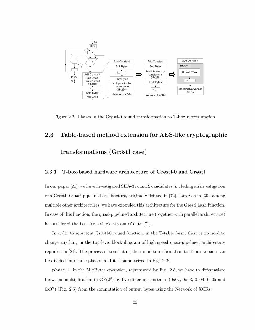
2.2 Phases in the Grøstl-0 round transformation to T-box representation. . . . 22
2.3 The Grøstl’s MixBytes operation . . . . . . . . . . . . . . . . . . . . . . . . 23
2.4 The Grøstl’s MixBytes operation based on reduced number of multipliers . 23
2.5 Grøstl’s MixBytes single input byte multiplication by five unique values . . 23
2.6 Grøstl’s MixBytes table implemented as 256x40 bits ROM . . . . . . . . . . 24
2.7 Grøstl’s round table implemented as 256x40 bits ROM . . . . . . . . . . . . 24
2.8 Block diagram of Grøsl and AES round . . . . . . . . . . . . . . . . . . . . 30
2.9 Shared MixColumns/Bytes . . . . . . . . . . . . . . . . . . . . . . . . . . . 32
2.10 Block diagram of Grøstl/AES core . . . . . . . . . . . . . . . . . . . . . . . 33
2.11 HMAC generation . . . . . . . . . . . . . . . . . . . . . . . . . . . . . . . . 36
2.12 Block diagram of AES-CTR where n is the number of AES cores . . . . . . 37
2.13 Pipelining in the Computational Unit of the Grøstl/AES core . . . . . . . . 39
2.14 High level scheduling in the Grøstl/AES core during encryption process . . 40
2.15 High level scheduling in the Grøstl/AES core during decryption process . . 40
3.1 (a) General concept of the parallel prefix addition, (b) Brent-Kung adder,
(c) Kogge-Stone adder. GP: gi = xi · yi, pi = xi ⊕ yi, S: si = pi ⊕ ci, :
g = g′′ + g′ · p′′, p = p′ · p′′ . . . . . . . . . . . . . . . . . . . . . . . . . . . . 53
x

3.2 Hybrid radix-2w carry save adder with the carry projection unit based on
parallel prefix network (PPN). Design X - Design I is based on Kogge-Stone
PPN and Design II is based on Brent-Kung PPN . . . . . . . . . . . . . . . 55
3.3 Implementation of the generate/propagate logic using fast carry chains and
LUTs of Xilinx FPGAs . . . . . . . . . . . . . . . . . . . . . . . . . . . . . 58
3.4 Modular adder based introduced in [20] . . . . . . . . . . . . . . . . . . . . 59
3.5 Modular adder based on the hybrid adder . . . . . . . . . . . . . . . . . . . 60
3.6 Test circuit for addition and modular addition . . . . . . . . . . . . . . . . 61
4.1 Modular adder/subtractor - high level block diagram . . . . . . . . . . . . . 74
4.2 Pipelined high-radix carry save modular adder/subtractor . . . . . . . . . . 74
4.3 High-radix carry save multi-operand adder . . . . . . . . . . . . . . . . . . 77
4.4 Block diagram of a multiplier based on 24x17 DSP units . . . . . . . . . . . 79
4.5 Additional circuit for the multiplier double speed mode support. (L RR =
(RR << 24·M2 ), L RC = (RC << 24·M
2 ), for (RR, RC) from left multiplier)
and (L RR = RR, L RC = RC, for (RR, RC) from right multiplier) . . . . 80
4.6 Block diagram of Barrett reduction for Solinas primes . . . . . . . . . . . . 85
5.1 Hierarchy of functions in pairing-based cryptosystems . . . . . . . . . . . . 93
5.2 Top level block diagram of pairing coprocessor . . . . . . . . . . . . . . . . 110
6.1 Timeline of the major cryptographic competitions . . . . . . . . . . . . . . 127
6.2 Relation between design flows of Altera and Xilinx and heuristic algorithms
in ATHENa . . . . . . . . . . . . . . . . . . . . . . . . . . . . . . . . . . . . 131
6.3 Dependency between requested and achieved frequency for combined opti-
mization targets . . . . . . . . . . . . . . . . . . . . . . . . . . . . . . . . . 135
6.4 ATHENa GMU optimzation 1 method for Xilinx devices . . . . . . . . . . . 136
6.5 ATHENa GMU optimzation 1 method for Altera devices . . . . . . . . . . . 137
6.6 Relative improvement of results from using ATHENa Virtex 5, 256-bit vari-
ants of hash functions. Ratios of results obtained using ATHENa suggested
options vs. default options of FPGA tools. [21] . . . . . . . . . . . . . . . . 138
xi

Abstract
DEVELOPMENT AND BENCHMARKING OF NEW HARDWARE ARCHITECTURESFOR EMERGING CRYPTOGRAPHIC TRANSFORMATIONS
Marcin Rogawski, PhD
George Mason University, 2013
Dissertation Director: Dr. Kris Gaj
Cryptography is a very active branch of science. Due to the everlasting struggle be-
tween cryptographers, designing new algorithms, and cryptanalysts, attempting to break
them, the cryptographic standards are constantly evolving. In the period 2007-2012, the
National Institute of Standards and Technology (NIST) held a competition to select a new
cryptographic hash function standard, called SHA-3. The major outcome of this contest,
apart from the winner - Keccak, is a strong portfolio of cryptographic hash functions. One
of the five final SHA-3 finalists, Grøstl, has been inspired by Advanced Encryption Stan-
dard (AES), and thus can share hardware resources with AES. As a part of this thesis,
we have developed a new hardware architecture for a high-speed coprocessor supporting
HMAC (Hash Message Authentication Code) based on Grøstl and AES in the counter
mode. Both algorithms provide efficient hardware acceleration for the authenticated en-
cryption functionality, used in multiple practical security protocols (e.g., IPSec, SSL, and
SSH). Our coprocessor outperforms the most competitive design by Jarvinen in terms of
the throughput and throughput/area ratio by 133% and 64%, respectively.
Pairing-based cryptography has emerged as an important alternative and supplement to
traditional public key cryptography. Pairing-based schemes can be used for identity-based

encryption, tripartite key exchange protocols, short signatures, identity-based signatures,
cryptanalysis, and many other important applications. Compared to other popular public
key cryptosystems, such as ECC and RSA, pairing-based schemes are much more compu-
tationally intensive. Therefore, hardware acceleration based on modern high-performance
FPGAs is an important implementation option. Pairing-schemes over prime fields are con-
sidered particularly resistant to cryptanalysis, but at the same time, the most challenging
to implement in hardware. One of the most promising optimization options is taking advan-
tage of embedded resources of modern FPGAs. Practically all FPGA vendors incorporate in
modern FPGAs, apart from basic reconfigurable logic blocks, also embedded components,
such as DSP units, Fast Carry Chain Adders, and large memory blocks. These hardwired
FPGA resources, together with meticulously selected prime numbers, such as Mersenne,
Fermat, or Solinas primes, can serve as a basis of an efficient hardware implementation. In
this work, we demonstrate a novel high-speed architecture for Tate pairing over prime fields,
based on the use of Solinas primes, Fast Carry Chains, and DSP units of modern FPGAs.
Our architecture combines Booth recoding, Barrett modular reduction, and the high-radix
carry-save representation in the new design for modular multiplication over Solinas primes.
Similarly, a low-latency modular adder, based on high-radix carry save addition, Fast Carry
Chains, and the Kogge-Stone architecture, has been proposed. The modular multiplier and
adder based on the aforementioned principles have been used as basic building blocks for
a higher level application - a high-speed hardware accelerator for Tate pairing on twisted
supersingular Edwards curves over prime fields. The fastest version of our design calculates
Tate pairing at the 80, 120 and 128-bit security level over prime fields in 0.13, 0.54 and 0.70
ms, respectively. It is the fastest pairing implementation over prime fields in the 120-128-bit
security range.
Apart of the properly designed architectures for cryptographic algorithms, one more
ingredient contributes to the success of a hardware coprocessor for any application - an
xiii

electronic design automation software and its set of options. Concerning this issue, Crypto-
graphic Engineering Research Group (CERG) at Mason has developed an open-source envi-
ronment, called ATHENa (Automated Tool for Hardware EvaluatioN), for fair, comprehen-
sive, automated, and collaborative hardware benchmarking and optimization of algorithms
implemented in FPGAs. One of the contributions of this thesis is the design of the heart of
ATHENa: its most efficient heuristic optimization algorithm, called GMU Optimization 1.
As a basis of its development, multiple comprehensive experiments have been conducted.
This algorithm has been demonstrated to provide up to 100% improvement in terms of the
throughput to area ratio, when applied to 14 SHA-3 Round 2 candidates. Additionally, our
optimization strategy is applicable to the optimization of dedicated hardware in any other
area of science and engineering.
Keywords: Cryptography, High-performance hardware architectures, Pairing-based
cryptography, modular arithmetic, authenticated encryption, heuristic methods for elec-
tronic design automation.
xiv

Chapter 1: Introduction
1.1 Motivation
New directions in Cryptography, namely Public Key Cryptography (PKC) discovery in
1976 by Diffie and Hellman [23], were introduced to solve the security problems such as
confidentiality, authenticity, integrity, non-repudiation and also secure key exchange during
communications in insecure networks. The first practical realization of PKC was RSA,
proposed by Ron Rivest, Adi Shamir and Len Adleman in 1977 [24].
A digital signature scheme is a mathematical algorithm for demonstrating the authen-
ticity of a digital message. Typically, digital signature is represented by a string of bits
which is dependent on some secret known only to the signer (known as the signer’s private
key) and the content of the document being signed. Signatures have to be easily verifiable
in case of a dispute about the origin of the document. An unbiased third party should be
able to resolve this issue undeniably, without accessing signer’s private key. Digital signa-
tures are used to implement three major security services: authentication, integrity, and
non-repudiation. Digital signatures are based on two main cryptographic transformations:
• a hash function, which takes an arbitrary size message and transforms it into a fixed-
size hash value (also known as message digest), and
• a digital signature scheme, which takes: a private key of the signer and a hash value of
the message to generate digital signature, and a public key of the signer, a hash value
of the message, and a digital signature to verify whether a given digital signature is
valid.
There are several security requirements for both algorithms: a hash function must be
0

Message
Alice
Message
Hash function Hash function
=
Signature
no
Alice’s private key
Signature
Alice’spublic key
yesschemeDigital signature
schemeDigital signature
Messagedigest
Message1digest
Messagedigest 2
Bob
Signature generation Signature verifiation
Figure 1.1: Digital signature generation and verification
irreversible and collision free and a digital signature scheme must be computationally infea-
sible to break. Digital signatures, key exchange and encryption schemes are used in a wide
variety of Internet security protocols, such as Secure Socket Layer (SSL), Internet Proto-
col Security (IPSec), Domain Name System Security Extensions (DNSSec), Secure Border
Gateway Protocol, etc. For example SSL uses digital signatures to authenticate secure web
servers to their clients all over the world.
In IPSec the most important handshaking mode for the Internet Key Exchange protocol,
apart from the key exchange support, is also based on a digital signature concept. The
Domain Name System Security Extensions (DNSSec) is a new protocol for binding IP
addresses and their domain names. The DNSSec requires digital signatures to provide strong
authentication within the chain of trust. An aggregate signature is useful for reducing the
size of certificate chains and for reducing message size in secure routing protocols such as
Secure Border Gateway Protocol. These are just a few high level protocols, which are the
basis of the security of any electronic information and in particular digital fund transfers
used in on-line shopping, bank transactions and e-documents circulation.
For cryptographic hash functions, two families of algorithms, commonly referred to as
SHA-1 and SHA-2, have been standardized by NIST, as described in the Federal Information
1
Processing Standard number 180 (the most current version is denoted FIPS-180-3). This
standard defines the following variants of both families: SHA-1, SHA-2/224, SHA-2/256,
SHA-2/384 and SHA-2/512. In 2005, a significant attack against SHA-1 was published
[25]. A similarity between the SHA-1 and the SHA-2 specification raises the question
about the possibility of extending this recently discovered attack to threaten the remaining
four versions of Secure Hash Algorithm. This potential weakness in SHA-2 can affect the
security of digital signature schemes based on this algorithm and finally, may undermine
the robustness of cryptographic services using these signatures.
The National Institute of Standard and Technology (NIST) developed a memorandum
with minimum key sizes for different security levels and for different underlying technologies.
A sensitive data which is required to be protected at least until 2030 must be guarded by
hash function SHA-2 with 256-bits output (SHA-3 will be an alternative solution), Advanced
Encryption Standard with 128-bit key, and by digital signature schemes based on RSA and
ECC technology with 3072 and 256-bits operands, respectively. The European Network
of Excellence for Cryptology (ECRYPT) released similar recommendation for key sizes.
However, it is stated in their work that the recommendations may need to be revised taking
into account more efficient attacks that are known to exist for discrete logarithm over binary
fields. The National Security Agency released the Fact Sheet NSA Suite B Cryptography
where the aforementioned requirements were confirmed, but it also recommends a transition
into elliptic curve systems instead of classical public key technology. This document provides
the recommendation for the underlying modular arithmetic, the prime fields must be used,
instead of binary and ternary fields.
Digital signature schemes and other cryptographic algorithms have been successfully
implemented on a large spectrum of platforms: starting from dedicated smart card chips,
through 8-bit microcontrollers, 32 and 64-bit microprocessors and finally, on high perfor-
mance application specific security processors.
In general, software solutions demonstrate:
• relatively low performance, and large power and energy consumption,
2

• difficulty in terms of generation truly random keys,
• vulnerability to software malware and a big class of side channel attacks (e.g. timing
attacks, cache attacks, etc.)
Contrary to software implementations, Application Specific Integrated Circuits (ASIC
technology) require long development time and a very expensive computer-aided design
(CAD) software. Moreover, after fabrication of an ASIC device, the designers cannot in-
troduce any upgrades to the implementation. ASIC-based solution are very costly in low
volumes, they require extensive and expensive testing, and the fabrication mistakes are
unrecoverable.
Cryptographic services, based on digital signature schemes, key exchange and encryption
schemes, are at the beginning of a new era. Novel basic cryptographic transformations,
based on the cutting edge underlying technology, for the the aforementioned schemes were
developed recently. They offer not only higher security, but also a set of new properties. It
is possible to apply them to a big range of new applications.
In case of cryptographic hash functions NIST has started a public competition for a new
SHA-3 function. Out of initial 51 candidates, only 5 algorithms were selected to the 3rd
and final round: BLAKE, Grøstl, JH, Keccak and Skein. In December 2012 Keccak has
been announced the winner of the contest.
Four major criteria were taken into account in the evaluation of these candidates are:
• security,
• performance in software,
• performance in hardware, and
• flexibility.
While security is commonly recognized as the most important evaluation criterion, it is
also a measure that is most difficult to evaluate and quantify, especially during a relatively
short period of time reserved for the majority of contests. So far all five SHA-3 final round
3

encryption
integrity
authentication
non−repudation
confidentiality
authenticated
encryption
key manegment
HMACTri−partite key
exchange1
Block ciphers
AES
43
addition
subtraction
multiplication
reduction
6eletronic design automation
optimal set of options for
SSHIPSec DNSSecSSL
5
SHA−3 competition
Hash functions
Tate pairing on
Edwards curves
Pairing transformations
2
applications
services
primitives
protocols
arithmetic
Identiy−basedCryptography
signatures
Figure 1.2: Hierarchical model of Cryptographic applications. Major contribution of thisresearch marked with points 1-6.
4

candidates demonstrate higher security margin than SHA-2 algorithm. Comprehensive
analysis of hardware and software implementations of final candidates was conducted by
multiple cryptographic engineering research groups all over the world. These studies show
potential throughput gain over solutions based on current standard. On the other hand
they also show that SHA-3 will be more expensive in terms of area used in hardware.
Pairing-based schemes can be used as basic building blocks for such high level protocols
like:
• identity-based encryption (identity used as a key for encryption),
• identity-based signatures (identity used as a key for signing),
• triparite key exchange (one round of computations allow the key agreement between
three parties)
• group signatures (a method for allowing a member of a group to anonymously sign a
message on behalf of the group),
• blind signatures (the content of a message is disguised before it is signed),
• aggregate signatures (given n signatures applied to n messages from n users, it is pos-
sible to aggregate all these signatures into a single signature which size is independent
of the number of users).
This novel technology bridges the gap between the classical Public Key and the Elliptic
Curve Cryptography.
In general pairing algorithms take two arguments two elliptic curve points P and Q
from two different algebraic groups G1 and G2 and it produces an element of the third
algebraic group GT .
The most important properties of these G1 x G2 → GT functions are:
• bilinearity ∀a, b ∈ Zp: e(aP, bQ) = e(P,Q)ab,
• non-degeneracy ( function e(P,Q) never returns ’1’)
5
• and efficiency in computations.
Different types of pairing functions were developed in the past, but for the prime fields
the most practical are the Tate and the Optimal Ate pairing transformations. Both of them
are based on the concept of iterative calculation (Miller’s algorithm [27]) of a new value of
pairing function for a given evaluation point, and a calculation of a new evaluation point.
The Tate pairing is most efficient for the ordinary Elliptic Curves and the Optimal Ate
pairing for a special class of - so called Barreto-Naehrig (B-N) curves.
In 2007 a new form of elliptic curves was discovered, so called Edwards curves. The
advantages of this new form are:
• the fastest reported in the literature unified procedure for addition and doubling
points,
• it is possible to embed those basic operations together with Tate pairing function
evaluation,
• twisted Edwards curves with extended projective coordinates are very easy for paral-
lelization and in fact potentially the most hardware-friendly.
In recent years implementations of cryptography on FPGAs became a popular subject
in academic research and in commercial security products. Historically, FPGAs have been
slower, less energy efficient and generally achieved lower physical security than their fixed
ASIC counterparts. Advantages include the ability to re-program in the field to fix bugs, a
shorter time to market, and lower non-recurring engineering costs. Some FPGAs have the
capability of partial re-configuration that lets one portion of the device be re-programmed
while other portions continue running.
In comparison to software implementations, FPGA-based cryptographic systems are
faster in majority of cases, they consume less power and they offer temper resistance and
overall higher security. In favor of general-purpose microprocessors software implementa-
tions have even higher flexibility and smaller development costs. Both software and FPGA
6

developers have an access to freely available design tools. One of the most important rea-
sons why FPGA-based cryptographic systems are successful is the specific nature of crypto-
graphic market and the requirements for commercial products in this sensitive area. In the
developed countries, the governments require that cryptographic products pass certification
process, They also demand to be involved in the design process of those solutions and to
have an access to their source codes. This general policy makes the cryptographic product’s
market suffer from a lack of global companies. In case of relatively small companies an
ideal solution for a cryptographic system, which requires high performance, capability for
upgrades, low volume, and a short time to market, are the FPGA devices.
This thesis aims to answer a question: Can the recent advances in the theory of Elliptic
Curves and pairing functions (namely the invention of Edwards Curves and its application
to the Tate pairing) and in the theory of hash functions (namely the development of the
SHA-3 standard) be exploited to develop the most efficient FPGA-based hardware archi-
tecture for the most important cryptographic services, outperforming all previously known
architectures with equivalent security?
1.2 Summary of research contributions
1.2.1 Novel hardware accelerator for authenticated encryption
SHA-3 finalist, hash function Grøstl, has been inspired by the Advanced Encryption Stan-
dard (AES). This unique feature can be exploited in a large variety of practical applications
(Fig. 1.2 pt. 1). In order to have a better picture of the Grøstl-AES computational efficiency
(high-level scheduling, internal pipelining, resource sharing, etc.), we designed a high-speed
coprocessor for the Grøstl-based HMAC and AES in the counter mode. This coprocessor
offers high-speed computations of both authentication and encryption with relatively small
penalty in terms of area and speed when compared to the authentication (original Grøstl
circuitry) functionality only. It is almost certain that the highest quality cryptographic
7

algorithms, like SHA-3 finalists, will find their niche applications.
For example: this coprocessor outperforms similar hardware accelerator proposed in [1]
for both IPSec modes: IP Encapsulating Security Payload (ESP) and Authentication Head-
ers (AH) by 64% and 8%, respectively. In case of the relatively rare the ESP’s encryption
mode only, the coprocessor from [1] is better by 44% as compared to our results.
Extracts of this work were published as joint work with Ekawat Homsirikamol and Kris
Gaj [28] and [29]
1.2.2 An adaptation of the T-box method to the AES-like hash functions
Joan Daemen, co-inventor of arguably two most important cryptographic standards - Ad-
vanced Encryption Standards (AES) and Secure Hash Algorithm (Keccak), proposed in his
PhD thesis, a provably secure method of building cryptographic transformation, the Wide
Trail Strategy. A block cipher SHARK was build upon this principle and a new, so called
Table-box method for very efficient implementation of this algorithm was published in 1996.
This mathod allows to redefine the round structure in a such a way, that it is friendly for
FPGA memory blocks. Several researchers have proposed hardware coprocessors for AES
based on the T-box method, which are the fastest [30], the most efficient [31], and imple-
mentation attacks resistant [32]. In our research we concentrated on the Wide Trail Strategy
progeny, the AES-based hash functions: ECHO, Fugue, Grøstl-0 and SHAvite-3 ((Fig. 1.2
pt. 2)). The efficiency of the hardware accelerators for aforementioned algorithms have
been improved up to 49, 173, 424 and 262 %, respectively. In this work, we have extended
our work for SHA-3 finalist, Grøstl. We have demonstrated, the best hardware accelerator
in terms throughput/area ratio, reported in open literature.
Extracts of this work were published as joint work with Rabia Shahid, Malik Umar Sharif
and Kris Gaj [33] and [34].
8
1.2.3 A novel, adder/subtractor for thousand bit and more using fast
carry chains of modern FPGAs
We have demonstrated a new, low latency, FPGA-oriented, hybrid adder ((Fig. 1.2 pt. 3)).
This adder efficiently combines the ideas of high-radix carry save addition based on the
fast carry chains, available on modern FPGA devices, and the parallel prefix network. The
implementation results reveals that this hybrid adder has a great potential for the addition
and modular addition of the long-size integers.
For example, our adder outperform, in terms of latency · area, both classical designs:
Kogge-Stone and Brent-Kung, on 1024, 2048 and 4096-bits addition up to 50, 38 and 35%,
respectively. At the same time, in terms of latency, our design is very competitive to the
both, commonly accepted, as the fastest adders in open literature.
Moreover, our hybrid high-radix carry save adder with carry projection unit based on
parallel prefix network have been applied to the 1024-bit modular addition circuit. The
implementation results on modern FPGA devices have proven that in terms of latency,
area and latency · area product, for Altera devices, have been improved over both classical
designs, on average 15, 40 and 55%, respectively. In case of Xilinx devices these numbers
were 50, 45 and 70%, respectively.
Extracts of this work were published as joint work with Kris Gaj and Ekawat Hom-
sirikamol [35].
1.2.4 New approach to arithmetic based on the Solinas primes for Pairing-
based Cryptography
A well known shortcut for a modular multiplication modulo a Mersenne number (2k − 1),
performing modular reduction without integer division has been generalized by Jerome A.
Solinas, a researcher from National Security Agency (NSA). The prime numbers generated
using his method and the fast arithmetic developed for them have been named after him.
9

These concepts have been such a important invention, that a big class of Solinas prime
numbers and their efficient arithmetic have been widely accepted, recommended and in fact
they became a part of a elliptic curved-based digital signature standard.
The aforementioned reduction technique is not applicable for all Solinas primes, in
particular for those which are used in Pairing-based Cryptography.
First, we have demonstrated that Solinas primes can benefit from the modified Barrett
reduction algorithm and then we have proposed conditions for efficient arithmetic based on
those primes. Next, we have optimized a grid method for multiplication to the geometry
of the digital signal processing blocks (DSP units), embedded in the structure of modern
FPGA devices.
This simple, thus very flexible design can give us some unique features - e.g.: it allows
to speed up single multiplication by using two multipliers. This special feature is especially
attractive in case of n multiplications, m available multipliers, and n dividing m. (e.g.:
a coprocessor build upon four multipliers, and a single iteration of the final exponentia-
tion algorithm in case of supersingular curves with embedding degree k = 2 requires 2
multiplications).
Finally, we have combined both concepts: grid multiplication method optimized for
FPGAs and the Barrett reduction for Solinas primes, and as a result we have obtained,
optimal, modular multiplier for pairing-friendly Solinas primes (Fig. 1.2 pt. 4).
Extracts of this work were published as joint work with Kris Gaj [36]
1.2.5 Novel hardware architectures for pairing on Edwards curves
We are going to demonstrate the first and the only to date, a high speed hardware accelerator
for the Tate pairing on twisted supersingular Edwards curves over prime fields (Fig. 1.2 pt.
5). Our hardware architecture is based on the set of algorithms presented in [37]. It can be
used directly to support emerging pairing-based protocols. This coprocessor was built upon
the hardware architectures proposed for Solinas primes and the hybrid high-radix carry save
10
and parallel prefix network adder. We demonstrate that combining aforementioned concepts
together with novel method for optimizations for final exponentiation, tight pipelining for
optimal number of processing units can improve an alternative software implementation by
a factor of 50 for three different security levels.
Finally, we have demonstrated, that even though Edwards curves were not optimized for
pairing, they present an interesting alternative to pairing friendly Barreto-Naehrig curves.
The implementation results, the hardware accelerator based on Stratix V, are elevating it,
to the top of the list of the fastest, to date, pairing solution over prime fields in a security
range 120-128-bits.
Extracts of this work were published as joint work with Kris Gaj [36]
1.2.6 A heuristic strategy for FPGA-oriented electronic design automa-
tion
In 2010 Cryptographic Engineering Research Group have introduced an open-source envi-
ronment, called ATHENa for fair, comprehensive, automated, and collaborative hardware
benchmarking of algorithms belonging to the same class. Apart from this primary use
for a fair evaluation of functionally equivalent digital system designs targeting FPGAs, a
major goal for this design automation system is an efficient search for the best set of op-
tions for a given optimization criterium. In this work we have demonstrated the design
rationale of the most successful heuristic optimization algorithm, the ATHENa’s heart,
GMU Optimization 1 (Fig. 1.2 pt. 6). This method helps to improve up to 100% through-
put/area ratio of hardware accelerators for major FPGA vendors and for functionally dif-
ferent digital circuits (e.g.: modular arithmetic, pairing systems, hash function and block
ciphers).
Extracts of this work were published as joint work with Kris Gaj, Jens-Peter Kaps,
Venkata Amriamieni, Ekawat Homsirikamol, and Benjamin Brewster in [38]. The heuristic
method ”GMU Optimization 1” helped to achieve the best to date hardware implementation
11

results in multiple our papers, including [39], [21], [40], [33], [28], [36] and [29].
12
Part I
High-performance hardware
architectures supporting
confidentiality and integrity
13
Chapter 2: High-Throughput hardware architectures of
AES-like Cryptographic hash functions
This chapter presents two unique hardware architectures for coprocessors sup-
porting AES-like hash functions. First, we demonstrate an adaptation of T-
table (also called T-box) method for the AES-based family of hash functions.
We have used SHA-3 finalist, Grøstl, to show that this method gives the best
throughput/area ratio for hardware implementations of this important class of
cryptographic transformations. Finally, we have demonstrated how to use Grøstl
and AES cipher similarities and convert them into a coprocessor which offers
high-speed computations of both authentication and encryption.
Contents
2.1 Introduction and motivation . . . . . . . . . . . . . . . . . . . . . 14
2.2 Previous work . . . . . . . . . . . . . . . . . . . . . . . . . . . . . 17
2.3 Table-based method extension for AES-like cryptographic trans-
formations (Grøstl case) . . . . . . . . . . . . . . . . . . . . . . . 22
2.4 Hardware architecture for the authenticated encryption based
on Grøstl and AES . . . . . . . . . . . . . . . . . . . . . . . . . . 28
2.1 Introduction and motivation
In the period 2007-2012, the National Institute of Standards and Technology (NIST) was
holding a hash competition [41] to select a new cryptographic hash function standard, called
14

SHA-3, for the purpose of superseding the functions in the SHA-2 family [42]. Performance
in hardware has been one of the major factors taken into account by NIST in the evaluation
of Round 2 and Round 3 candidates during the SHA-3 competition [41], [43], [44]. This
factor was particularly important in the final round of the contest, because the algorithms
qualified to this round were not very likely to have any significant security weaknesses.
On October 2, 2012, Keccak [45] has been announced to be the winner of the NIST hash
function competition [46]. This algorithm has demonstrated medium speed in software
implementations [47], [48], and the best results in terms of hardware efficiency for both
single stream [43] and multiple streams of data in hardware implementations [39].
Beyond any doubt, cryptographic standards for block ciphers: AES [49] and 3DES [50]
and hash functions SHA-2 [42] and newly selected future standard - Keccak [45] are the
most important crypto-algorithms for both Academia and Industry.
The SHA-3 competition was very similar in many aspects to the AES competition [51]:
both were open and fully transparent contests, organized by NIST. They have received rel-
atively big attention from the cryptographic community and the final result was announced
after multiple years of intensive investigations in the area of security, hardware and software
performance. The major outcome from both contests seems to be as well as very similar -
a strong portfolio of cryptographic transformations.
Apart from the winner of AES contest, almost all finalists have been either implemented
in different commercial products (e.g.: [52], [53], [54]) or they were patented [55]. It is almost
certain that the highest quality cryptographic algorithms, like SHA-3 finalists, will find their
niche applications.
The main objective of almost all SHA-3 related studies was to evaluate all candidates
using a uniform approach, and therefore the unique features of each and every function were
not deeply investigated.
There are relatively few works that discuss any distinctive hardware architectures for
the SHA-3 candidates. A coprocessor supporting Skein in tree hashing mode was presented
in [56]. Common architectures of the block cipher AES and the Round 2 versions of Grøstl-0
15

and Fugue algorithms were reported in [1]. Recently, a high-speed AES-Grøstl architecture
was also reported in [57].
A compact implementation of the block cipher Threefish and the Round 3 hash algorithm
Skein was demonstrated in [58]. Three outstanding low-area, resource-sharing oriented
coprocessors, for combinations: Round 3 version of Grøstl/AES and ECHO/AES were
proposed, designed and discussed in [59], [60] and [61], respectively.
The similarities between AES and Grøstl (or any other AES-like hash function - Fig.
2.1) lead us to two, unique and important architectures.
First of all, the majority of AES hardware accelerators implement a single round in a
straightforward way or using loop-unrolling, pipelining techniques for FPGAs, utilizing a
vast amount of user logic elements. This approach, based on a traditional configurable logic
utilization, help to maintain platform independence, and therefore it does not exploit the
full potential of modern FPGA devices. Contrary, the T-table method, described in [62],
Sec. 4.2 enables the memory-oriented re-definition of AES round, and it eventually leads
to the highly efficient hardware architecture of AES.
To the best of our knowledge, our work [33] was the very first one, which demonstrated
a T-table-based representation of Grøstl-0 (and also ECHO, Fugue and SHAvite-3).
Second important implication of this compatibility between the current encryption stan-
dard, AES and the whole family of AES-derived hash function is their joint use for authen-
ticated encryption. A typical application for such cryptographic service could be Secure
Socket Layer [63], Transport Layer Security [64], Secure Shell [65] and Internet Protocol
Security [66–68].
The rest of this chapter is organized as follows:
In Section 2.2 we discuss relevant previous work. Section 2.3 is devoted to the description
of the T-table architecture of Grøstl. Section 2.4 demonstrates the design of a hardware
coprocessor for authenticated encryption.
16

2.2 Previous work
2.2.1 Grøstl in SHA-3 competition
In January 2011, Grøstl team published tweaks to their specification of Grøstl [69], [17]. An
algorithm described by the original Grøstl specification [70] has been renamed to Grøstl-0,
and the tweaked version of Grøstl, described by the revised specification [17], is from this
point-on called Grøstl. The proposed tweaks are aimed primarily at the increase in the
algorithm resistance to cryptanalysis [69]. This increased resistance in security, typically
comes together with some limited penalty in terms of performance in hardware [71].
Grøstl-0 has been implemented by several groups in FPGAs and ASICs [43]. In this
chapter, we focus on implementations targeting FPGAs and optimized for high speed rather
than low area. High-speed implementations of Grøstl-0 typically use two major architec-
tures. In the first architecture, reported first in [70], permutations P and Q are implemented
using two independent units, working in parallel. We call this architecture parallel architec-
ture. In the second architecture, introduced in [72], the same unit is used to implement both
P and Q. This unit is composed of two pipeline stages that allow interleaving computations
belonging to permutations P and Q. We call this architecture quasi-pipelined architecture,
as it is based on the similar principles as the quasi-pipelined architectures of SHA-1 and
SHA-2 reported in [73], [74]. The details of the quasi-pipelined architecture of Grøstl-0 are
described in [72] (Section 9), [75] (Section 3.8) and [76] (Section V).
An analysis of the influence of the Round 3 tweaks in Grøstl on the performance of
this algorithm in FPGAs was conducted in [71]. Comprehensive hardware evaluation across
multiple architectures for all SHA-3 finalists, including Grøstl, was investigated in [39] and
[81]. The implementation results of hardware architectures, for a single stream of data, in
both variants of Grøstl-256 are summarized in Table 2.1.
17

Table 2.1: Results of Implementations for High-Speed Architecturesof Grøstl-256, using Xilinx Virtex 5 FPGAs.
Source Memory Frequency Throughput Area Throughput/Area[BRAM] [MHz] [Mbps] [Slice] [Mbps/Slice]
Grøstl-0 - Round 2
Gauravaram et al. [70] N/A 200.7 10276 1722 5.97
Jungk et al. [76] 17 295.0 7552 1381 5.46
Shahid et al. [40] 48 250.0 6098 1188 5.13
Homsirikamol et al. [75] 0 323.4 7885 1597 4.94
Gaj et al. [21] 0 355.9 8676 1884 4.61
Matsuo et al. [77] 0 154.0 7885 2616 3.01
Baldwin et al. [78] 0 101.3 5187 2391 2.17
Kobayashi et al. [79] 0 101.0 5171 4057 1.27
Guo et al. [80] 0 80.2 4106 3308 1.24
Baldwin et al. [78] 0 101.3 3242 2391 1.36
Baldwin et al. [78] 0 78.1 2498 2579 0.97
Grøstl - Round 3
Sharif et al. [33] 18 226 5524 1141 4.84
Gaj et al. [81] 0 251 6117 1795 3.41
Homsirikamol et al. [39] 0 249 6072 1912 3.18
Homsirikamol et al. [39] 0 158 8081 2591 3.12
2.2.2 T-box method
Joan Daemen, in his PhD thesis [2], proposed the Wide Trail Strategy. It is a method of
constructing highly efficient block ciphers, which are provably secure against major crypt-
analytical attacks.
This Wide Trail Strategy became a design rationale of several cryptographic transfor-
mations (Fig. 2.1). Most of them demonstrate not only the hardware-software efficiency
and flexibility, but also an elegance in their description.
Fig. 2.1 presents the timeline development of the aforementioned class of cryptographic
transformations.
In paper [3], Shark ((Fig. 2.1 pt. 4) pt. 1) was proposed together with its efficient
implementation methods. This paper demonstrated how to combine several simpler mathe-
matical transformations into one operation equivalent to a round. This method was named
table implementation, T-table or T-box implementation.
To the best of our knowledge, the first attempt of the adoption of this method for the
hardware implementation of the AES round was proposed by Fischer and Drutarovsky in
18

Joan Daemen PhD’s Wide Trail Strategy progeny − AES family
AES(2007−2012)
SHA−3
Noekeon
(2000−2003)
NESSIE
Anubis
Crypton
Square
Q
JH
Khazad
Grand Cru
Twofish
Serpent 4
3
2
1
block ciphers hash functions
BaseKing/3way
ECHO
Shark
Rijndael (AES)
Hierocrypt
Shavite−3
Fugue
Groestl
(1995−1997)
pre−AES work
(1997−2000)
Figure 2.1: Wide Trail Strategy family of cryptographic transformations was defined in[2]. Based on this strategy several algorithms have been invented: Shark [3], Square [4],
BaseKing [2], Rijndael-AES [5], Serpent [6], Twofish [7], Crypton [8], Hiercorypt [9],Khazad [10], Anubis [11], GrandCru [12], Q [13], Noekeon [14], ECHO [15], Fugue [16],
Grøstl [17], SHAvite-3 [18] and JH [19]
19

[31] (Fig. 2.1 pt. 2). Contrary to that implementation the design, described by Drimer
et al. in [30], maps the complete AES data path onto embedded elements contained in
Virtex-5 FPGAs. This strategy provides most savings in logic and routing resources and
results in the highest data throughput on FPGAs reported in open literature.
Taking into account the fact that the whole AES family (Fig. 2.1) is built upon similar
principles, several implementational nuances can be inherited. We have proposed archi-
tectural improvements, using aforementioned technique, for block cipher Hierocrypt in [34]
(Fig. 2.1 pt. 3) and hash functions: ECHO, Fugue, Grøstl-0 and SHAvite-3 in [33] (Fig.
2.1 pt. 4). Table 2.2 summarizes the geometry of the T-tables reported in open literature.
Table 2.2: Table-based hardware architectures of cryptographic transformations. T-boxgeometry AxB is defined by A-bit address space and B-bit words.
algorithm T-box size source
Block Ciphers
AES 8x32 Fischer et al. [31], Drimer et al. [30]Hierocrypt-3 8x32 Rogawski [34]
Hash Functions
Grøstl-0 8x40 Shahid et al. [40]Fugue 8x24, 8x32 Shahid et al. [40]ECHO 8x32 Shahid et al. [40]SHAvite-3 8x32 Shahid et al. [40]Grøstl 8x40 ch. 2.3
2.2.3 Resource sharing
The idea of hardware resource sharing is very practical and especially attractive in indus-
trial applications. Several companies offer so called all-in-one cryptographic solutions. For
example, [82] and [83] offer customized cores, including sophisticated AES core, which sup-
ports 128, 192 and 256-bit main key and several different operational modes in a single chip.
This concept was also investigated by academia: shared MD5 and SHA-1 implementation
was described in [84–86], MD5 implemented together with RIPEMD-160 was reported in
[87], a combined SHA-1, MD-5 and RIPEMD-160, core was discussed in [88]. Fugue with
20

Table 2.3: Hardware architectures supporting authenticated encryption at 128-bit security
Source Algorytms FPGA Frequency Area Throughput Throughput/Area[MHz] [Slice/LE] [Mbps] [Mbps/(Slice/LE)]
Balanced designs
Rogawski et al. [28] Grøstl-0 and AES Cyclone III 159.9 23039 2640 0.12
Jarvinen [1] Grøstl-0 and AES Cyclone III 53.4 13723 9561 0.07
Jarvinen [1] Fugue and AES Cyclone III 59.8 4875 2731 0.06
Low area designs
At et al. [90] Grøstl and AES2 Virtex-6 393 1694 64.61 0.38
Beuchat et al. [91] ECHO and AES3 Virtex-6 397 1555 62.61 0.40
At et al. [58] Skein and Twofish Virtex-6 276 1325 40.01 0.301 throughput recalculated for authenticated encryption based on HMAC-(hash function) and CTR-(block cipher)
2 this design offers Grøstl-256, Grøstl-512, AES-128, AES-192 and AES-2563 this design offers ECHO-256, ECHO-512, AES-128, AES-192 and AES-256
4 this design uses one extra block RAM5 this design uses two extra block RAMs
AES core, and Grøstl-0 with AES core, were reported in [1]. Based on this trend, the practi-
cality of combining different cryptographic services, confidentiality and authentication, into
a single coprocessor by sharing resources as much as possible is a favored approach by the
industry and academia. Table 2.3 summarizes the related work in this area.
Alternatively, a partial reconfiguration method can be used to conserve space at the
cost of reconfiguration time penalty, as well as limiting hardware operating life, due to the
limited number of times the chip can be configured. This approach has been demonstrated
in the combined AES, SHA-2 and a modular multiplication core in [89].
A typical application for resource sharing-based coprocessor will be the IPSec protocol
suite [66] for securing the Internet Protocol, which is the basis of Internet. This suite consists
of the Authentication Header Protocol (providing authentication only) and Encapsulating
Security Payload (providing confidentiality and optional authentication at the same time).
21
!"#$
%&
'(()*+,-./,.!01)23.4-
5"678464,.4()9,):+;9<=
!>9?.)23.4-
@9A)23.4-
#"!$
"B
%&
'(()*+,-./,.
!01)23.4-
!>9?.)23.4-
@08.9789</.9+,)13)<+,-./,.-)9,)CD5EF%=
G4.H+IJ)+?)K$L-
'(()*+,-./,.
!01)23.4-
!>9?.)23.4-
@08.9789</.9+,)13)<+,-./,.-)9,)CD5EF%=
G4.H+IJ)+?)K$L-
'(()*+,-./,.
CI+4-.8)M2+A
@+(9?94()G4.H+IJ)+?)K$L-
2L'@
Figure 2.2: Phases in the Grøstl-0 round transformation to T-box representation.
2.3 Table-based method extension for AES-like cryptographic
transformations (Grøstl case)
2.3.1 T-box-based hardware architecture of Grøstl-0 and Grøstl
In our paper [21], we have investigated SHA-3 round 2 candidates, including an investigation
of a Grøstl-0 quasi-pipelined architecture, originally defined in [72]. Later on in [39], among
multiple other architectures, we have extended this architecture for the Grøstl hash function.
In case of this function, the quasi-pipelined architecture (together with parallel architecture)
is considered the best for a single stream of data [71].
In order to represent Grøstl-0 round function, in the T-table form, there is no need to
change anything in the top-level block diagram of high-speed quasi-pipelined architecture
reported in [21]. The process of translating the round transformation to T-box version can
be divided into three phases, and it is summarized in Fig. 2.2:
phase 1: in the MixBytes operation, represented by Fig. 2.3, we have to differentiate
between: multiplication in GF(28) by five different constants (0x02, 0x03, 0x04, 0x05 and
0x07) (Fig. 2.5) from the computation of output bytes using the Network of XORs.
22

, I and O are 64−bit input and output, respectively.O
02 02 03 04 05 03 05 0707 02 02 03 04 05 03 05
05 07 02 02 03 04 05 0303 05 07 02 02 03 04 0505 03 05 07 02 02 03 0404 05 03 05 07 02 02 03 03 04 05 03 05 07 02 02 02 03 04 05 03 05 07 02
*O[3]
O[6]O[7]
O[0]O[1]O[2]
O[4]
O[5]
I[0]I[1]I[2]I[3]I[4]I[5]I[6]I[7]
= MxI
Figure 2.3: The Grøstl’s MixBytes operation
I[i+7]
07
05
04
03
02
I[i] * I[i+1] *
02
03
04
05
07
I[i+2] *
02
03
04
05
07
I[i+3] *
02
03
04
05
07
I[i+4] *
02
03
04
05
07
I[i+5] *
02
03
04
05
07
I[i+6]
02
03
04
05
07
* *
02
03
04
05
07
O[i]
O[i+1]
O[i+2]
O[i+3]
O[i+4]
O[i+5]
O[i+6]
O[i+7]
O = MxI
Figure 2.4: The Grøstl’s MixBytes operation based on reduced number of multipliers
In the MixBytes operation every single byte is multiplied by eight values in Matrix
B [92], [69]. Following the idea from [31], we would represent our T-boxes as 8x64 bit
substitution box tables. However, due to the fact that there are only five unique values in
Matrix B (Fig.: 2.4), our proposed Grøstl-0 T-box has the dimensions 8x40 (8-bit address
bus width, 40-bit words).
phase 2: the operations of Multiplication by constants in GF(28) and S-box transfor-
mation both produce 8 bits of output for every 8 bits of input. Therefore, it is possible
S[i] − output from S−box
vector multiplication by matrix
x 02 x 03 x 04 x 05 x 07
T[i]i = 0,1, ... 7
S[i]
T[i] − input to the network of XORs in
Figure 2.5: Grøstl’s MixBytes single input byte multiplication by five unique values
23

00 00 00 00 00
02 03 04 05 07
0xFF
0xFE
0x00
0x01
E7 19 D5 2B CC
E5 1A D1 2E CB
.... .... .... .... ............
x02 x03 x04 x05 x07
Figure 2.6: Grøstl’s MixBytes table implemented as 256x40 bits ROM
0xFF
0xFE
0x00
0x01
.... .... .... .... ............
C6 A5 97 F4 32
F8 84 EB 97 6F
6D D6 DA 61 0C
2C 3A 58 4E 62
x02 x03 x04 x05 x07
Figure 2.7: Grøstl’s round table implemented as 256x40 bits ROM
to combine them. Since there are five different constants used in multiplications, then for
every single byte there are always 5 bytes produced. We can define a look-up table with
256 words (8 bit address bus) which consist of 5-byte-wide words. One of the property of
both AES and Grøstl-0 is the horizontal symmetry (every byte goes through the same set
of operations) in SubBytes, ShiftBytes and MixBytes (ShiftRow and MixColumn in AES).
This allows us to move the ShiftBytes operation after Multiplication by constants.
phase 3: since ShiftBytes is a simple operation, which is implemented using routing
resources only in hardware, it is possible to merge this operation together with the network
of XORs operation.
Such defined Grøstl-0 T-box round can be implemented in configurable logic, but due
to the fact that there are 64 (in Grøstl-0-256) and 128 (in Grøstl-0-512) such 256x40 bits
24

loop-up tables for quasi-pipeline architecture (and this number is doubled for parallel archi-
tecture), a large number of regular logic resources is going to be occupied, and clearly there
is no benefit from such a solution. However, if we implement this operation using embed-
ded memories, both parallel and quasi-pipelined architecture can benefit from the Grøstl-0
T-box round representation. The quasi-pipelined architecture [75] was used for our T-box
implementation. The pipeline register between SubBytes and ShiftBytes from this archi-
tecture was implemented as a part of the registered output from FPGA block memory. We
used inference method for the implementation of the T-box in a block memory in VHDL.
Because of the restrictions on the maximum word size in the Virtex 5 BRAM, we have
divided a 256x40 bit memory into two memories with the dimensions, 256x32 and 256x8,
respectively.
Tweaks introduced to the Grøstl specification do not affect the Grøstl T-box definition
(i.e., this definition is common for both Grøstl-0 and Grøstl). The only change that have
to be introduced concerned both AddRoundConstant and the Modified Network of XOR
operations.
2.3.2 Implementation results
In this section, we present a comparison between the basic designs, implemented using
reconfigurable logic, and embedded designs, with Block Memories. All basic designs are
identical to those described in detail in [21]. All the embedded designs were, so called,
T-box-based architectures with T-box tables implemented using block memories.
In Table 2.4, we demonstrate comprehensive results of throughput analysis across two
high-performance (Xilinx Virtex-5 and Altera Stratix III) and two low-cost FPGA families
(Xilinx Spartan 3 and Altera Cyclone II). We optimized the designs to achieve comparable
throughput while replacing logic with embedded resources. However, we observed a signif-
icant drop in frequency and throughput across high-performance families. In case of the
selected low-cost families the frequency, and consequently the throughput, were consistently
25

Table 2.4: Timing characteristics and resource utilization for basic architectures andarchitectures based on the T-box method in case of four selected FPGA families.Notation: Tp - throughput, Mem-bits - number of memory bits, ∆ Tp - relativeimprovement in throughput, ∆ Area - relative reduction in the number of basicreconfigurable resources, ∆ Tp/Area - relative improvement in throughput/area
Algorithm Architecture Tp Area Tp/Area ∆ Tp ∆ Area ∆ Tp/Area
Altera Cyclone II 1
Mbps #LEs,#Mem-bits
Tp/#LEs % % %
FugueBasic 1490 5825, 0 0.26 23.3 55.6 173.5T-box 1837 2855, 99k 0.71
Grøstl-0Basic 3086 18901, 0 0.16 6.9 79.2 424.4T-box 3300 3933, 528k 0.84
GrøstlBasic 2909 19176 0.15 13.0 79.1 446.7T-box 3288 4012, 640k 0.82
SHAvite-3Basic 1366 10165, 0 0.13 5.0 70.1 262.3T-box 1434 3044, 256k 0.47
Altera Stratix III
Mbps #ALUTs,#Mem-bits
Tp/#ALUTs % % %
ECHOBasic 13395 20754, 0 0.64 -16.8 36.6 49.8T-box 11146 13159, 2048k 0.96
FugueBasic 3241 2391, 0 1.36 -6.8 34.2 41.6T-box 3022 1574, 99k 1.92
Grøstl-0Basic 6990 6290, 0 1.12 -33.5 63.5 82.0T-box 4950 2288, 528k 2.03
GrøstlBasic 6008 7386, 0 0.81 -2.7 62.3 158.0T-box 5848 2788, 640k 2.09
SHAvite-3Basic 3295 2930, 0 1.12 15.4 49.6 129.0T-box 3804 1477, 256k 2.58
Xilinx Spartan 3 1,2
Mbps #slices,#BRAMs
Tp/#slices % % %
FugueBasic 1231 2493, 0 0.49 13.7 37.5 83.5T-box 1400 1558, 8 0.90
SHAvite-3Basic 1094 4017, 0 0.27 24.5 50.0 151.1T-box 1362 2008, 16 0.68
Xilinx Virtex 5 1
Mbps #slices,#BRAMs
Tp/#slices % % %
FugueBasic 3469 712, 0 4.87 -8.8 19.4 13.1T-box 3165 574, 8 5.51
Grøstl-0Basic 8057 1629 4.95 -24.3 27.0 3.7T-box 6098 1188, 48 5.13
GrøstlBasic 6117 1795 3.41 -4.5 39.7 58.4T-box 5840 1083, 48 4.19
SHAvite-3Basic 3242 1028, 0 3.15 8.9 24.0 43.5T-box 3530 781, 16 4.52
1ECHO did not fit entire description of T-box into embedded memory in Spartan-3, Virtex-5 and Cyclone II2 Grøstl-0 and Grøstl did not fit entire description of T-box into embedded memory in Spartan-3
26

improved.
This behavior can be explained as follows: In Spartan 3, basic implementation of an
AES S-box costs 64 slices based on 4-input LUTs. For Virtex 5, the cost is 8 slices based
on 6-input LUTs. The corresponding number of LUT levels is 5 for Spartan 3, and 2 for
Virtex 5. Moving to the T-box based implementations in Spartan 3 replaces the large
routing delay inside of an S-box, by a medium routing delay between logic and BRAMs.
The same transition in Virtex 5, replaces the small routing delay inside of an S-box, by a
larger routing delay between logic and BRAMs.
Cyclone II does not contain distributed memory (i.e., memory inside of basic Logic
Elements, LE) As a result, in the basic architecture, each S-box is first converted to a set of
Boolean functions, and then these functions are mapped into 4-input combinational LUTs.
The result amounts to 208 Logic Elements and 7 levels of LUTs per each S-box. This
transition is obviously quite costly in terms of performance. The embedded T-box based
designs can take advantage of 4 kbit memory blocks present in Cyclone II, and as a result
are more efficient. In Stratix III, compared to Cyclone II, larger and more flexible Adaptive
Look-up Tables (ALUTs) are used for implementing S-boxes. As a result, basic designs,
with a small number of ALUT levels, are relatively faster than embedded designs, which
suffer from the relative large interconnect delays between reconfigurable logic and memory
block.
AES-based functions, in both S-box and T-box architectures, resulted in much bigger
area reduction because the functions implemented using embedded resources are a big part
of the entire hash function circuit. In case of functions using round constant tables (JH,
Keccak), the relative improvement is not significant because these tables are relatively small
[33] and [40].
27
2.3.3 Conclusions
Future designers interested in using embedded resources do need to consider right FPGA
family selection for their implementations because FPGA vendors have different features
and architectures for embedded resources. Our results show a significant, but not consis-
tent improvement in terms of efficiency (throughput/area) across FPGA families. From
a few percents of relative improvement of throughput/area ratio in Xilinx Virtex-5 to the
impressive 400% in case of Altera Cyclone II.
2.4 Hardware architecture for the authenticated encryption
based on Grøstl and AES
2.4.1 Authenticated encryption in IPSec
Internet Protocol Security (IPSec) provides security against attacks on data transmitted
over the Internet through security services facilitated by a set of protocols. It was designed
to operate at the level of the Internet layer according to the OSI network model. This
makes it completely transparent to applications and users.
The security services provided by the Internet Protocol Security (IPSec) include:
• Confidentiality - Prevents unauthorized access to the transmitted data.
• Data integrity - Ensures data was not altered during transmission.
• Authentication - Enables the identification of the information source.
The IPSec series of protocols makes use of various cryptographic algorithms, such as
ciphers, hash functions and key agreement schemes, in order to provide security services.
The Internet Key Exchange (IKEv2) protocol in version two has to be used to establish
secure connections, so called Security Associations (SAs). The IKEv2 uses cryptographic
28

Table 2.5: IPSec Supported Protocols and Algorithms
Protocol Security Service Provided Supported Algorithm
ESP confidentiality through encryption and op-tional data integrity
AES in CBC or CTR mode and HMAC-SHA-256
AH connectionless integrity and data originauthentication
HMAC-SHA1-96, AES-XCBC-MAC-96,HMAC-SHA-256
IKE negotiates connection parameters, includ-ing keys
Diffie-Hellman scheme and AES in PRNGmode
algorithms: key exchange algorithm (Diffie-Hellman) and pseudo random function based on
the Advanced Encryption Standard (AES) in XCBC mode (AES-XCBC-PRF-128).
The Authentication Header (AH) protocol provides connectionless integrity and data
origin authentication. The AH uses Hashed Message Authentication Code (HMAC) with
Secure Hash Algorithm (SHA).
The Encapsulating Security Payload (ESP) protocol provides mechanisms for both con-
fidentiality and data integrity services. In order to provide both cryptographic functions,
the AES in Cipher-Block-Chaining (CBC) and/or Counter (CTR) modes of operation and
HMAC based on SHA-2 are used.
To assure protection and standardization, the minimum set of cryptographic algorithms
that must be supported by an implementation of IPSec for ESP, AH and IKEv2 protocols,
as stated in [67], is illustrated in Table 2.5.
2.4.2 Contribution
In our paper [28], we have demonstrated that both algorithms (128-bit security level ver-
sions) can be used to build a coprocessor supporting both ESP and AH protocols. However,
in case of the ESP protocol we have investigated only the case of the encryption process.
In this effort we will present that the idea of a hardware coprocessor for Grøstl and AES
with a common data-path is also applicable to:
• the authenticated decryption process in the ESP protocol for 128-bit security level,
• the HMAC-Grostl for 256-bit security level in the AH protocol.
29
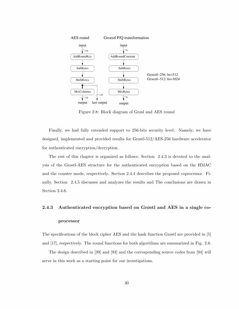
Groestl−512: bs=1024
128
AddRoundKey
SubBytes
128
128
MixColumns
ShiftRows
Groestl P/Q transformationAES round
input
AddRoundConstant
MixBytes
ShiftBytes
SubBytes
bs
bs
input
output last output output
Groestl−256: bs=512
Figure 2.8: Block diagram of Grøsl and AES round
Finally, we had fully extended support to 256-bits security level. Namely, we have
designed, implemented and provided results for Grøstl-512/AES-256 hardware accelerator
for authenticated encryption/decryption.
The rest of this chapter is organized as follows: Section 2.4.3 is devoted to the anal-
ysis of the Grøstl-AES structure for the authenticated encryption based on the HMAC
and the counter mode, respectively. Section 2.4.4 describes the proposed coprocessor. Fi-
nally, Section 2.4.5 discusses and analyzes the results and The conclusions are drawn in
Section 2.4.6.
2.4.3 Authenticated encryption based on Grøstl and AES in a single co-
processor
The specifications of the block cipher AES and the hash function Grøstl are provided in [5]
and [17], respectively. The round functions for both algorithms are summarized in Fig. 2.8.
The design described in [39] and [93] and the corresponding source codes from [94] will
serve in this work as a starting point for our investigations.
30

Grøstl and the AES comparison
In order to extend the original Grøstl hardware architecture several facts have to be taken
into consideration:
• The basic round structures of both algorithms are demonstrated in Fig. 2.8. All
four corresponding transformations have the same order in both AES and Grøstl. Due
to this fact a resource sharing between both algorithms is especially attractive. It is
expected that the delay in the critical path in both cases should be very similar.
• The SubBytes layers in both cases are built upon the same substitution box (S-
box), therefore they can be fully shared (Fig. 2.10, pt. 1). In terms of circuit area,
this transformation is the most costly out of all operations of the Grøstl and AES
rounds.
• The ShiftRows and ShiftBytes transformations in AES and Grøstl, respectively,
can be implemented as a permutation of bytes (simple rewiring). However, since they
are not similar, both operations have to be implemented separately and properly
multiplexed (Fig. 2.10, pt. 2).
• The AddRoundKey and the AddRoundConstant transformations in AES
and Grøstl, respectively, can be implemented as a simple network of XOR gates.
However, since they are not similar, both operations have to be implemented sepa-
rately and properly multiplexed (Fig. 2.10, pt. 3).
• The MixColumns and the MixBytes (Fig. 2.10, pt. 4) in AES and Grøstl,
respectively, share the GF(28) multiplication by constants: 0x02 and 0x03. Therefore
they can be merged together (Fig. 2.9, pt. 1). The networks of output XORs require
two separate paths (Fig. 2.9, pt. 2-3) for both algorithms. The MixColumns and
MixBytes operations have to be multiplexed accordingly (Fig. 2.9, pt. 4).
• The last round of the AES block cipher is different than the regular round. Therefore
31

24
x4
x2
x3
x7
x5
i[7..0] − 64−bit input to MixColumns/MixBytes
o[7..0] − 64−bit output from MixColumns/MixBytes
a[7..0] − 64−bit output from MixColumns
g[7..0] − 64−bit output from MixBytes
m[i][5..0] − i−th byte results of multiplication
by constants
in Groestl MixBytesNetwork of XORs
3
4
m[7][1]
m[7][2]
m[7][3]
m[7][4]
m[7][5]
m[7][0]
8
i[7]
m[7][5..0]
48
$cm_{\#7}$ m[0][5..0]
48
i[0]
8
$cm_{\#0}$
a[3] a[0]
m[3][5..3]
m[2][5..3]
m[1][5..3]
m[0][5..3]
a[7] a[4]
m[6][5..3]m[7][5..3]
m[4][5..3]
m[5][5..3]
Network of XORs in AES MixColumns
Network of XORs in AES MixColumns
1
2
m[7][4..0] m[0][4..0]
40 40
g[7] g[0]
o[7..0]
64
g[7..0]a[7..0]24
Figure 2.9: Shared MixColumns/Bytes
32

01
b
SubBytes
ks
ks
Groestl−256 : b=512
AES:
Groestl−512 : b=1024
ks=b/4
SIP
O
IV
h
ShiftBytes
0 1
b+ks ks
b
7’0’
ShiftRows
KeyExpansion
01
01
10
AddRoundKey
1 0
01
1 0
8
11
9
2
4
5
6
R1
R2
AddRoundConstant
R0
R3 R4
012
ctr
0 1 2
b/2
01
unless specified otherwise.All buses are b−bit wide
10
SharedMixBytes
64din
3
1
64
dout
PISO
LastRdSubKey
RdSubKey
LastRdSubKey
0x80 ... 02
P/Q
Figure 2.10: Block diagram of Grøstl/AES core
33
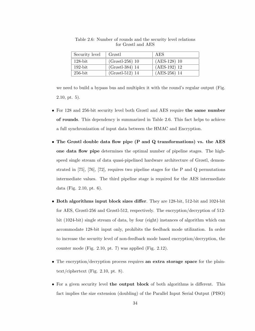
Table 2.6: Number of rounds and the security level relationsfor Grøstl and AES
Security level Grøstl AES
128-bit (Grøstl-256) 10 (AES-128) 10
192-bit (Grøstl-384) 14 (AES-192) 12
256-bit (Grøstl-512) 14 (AES-256) 14
we need to build a bypass bus and multiplex it with the round’s regular output (Fig.
2.10, pt. 5).
• For 128 and 256-bit security level both Grøstl and AES require the same number
of rounds. This dependency is summarized in Table 2.6. This fact helps to achieve
a full synchronization of input data between the HMAC and Encryption.
• The Grøstl double data flow pipe (P and Q transformations) vs. the AES
one data flow pipe determines the optimal number of pipeline stages. The high-
speed single stream of data quasi-pipelined hardware architecture of Grøstl, demon-
strated in [75], [76], [72], requires two pipeline stages for the P and Q permutations
intermediate values. The third pipeline stage is required for the AES intermediate
data (Fig. 2.10, pt. 6).
• Both algorithms input block sizes differ. They are 128-bit, 512-bit and 1024-bit
for AES, Grøstl-256 and Grøstl-512, respectively. The encryption/decryption of 512-
bit (1024-bit) single stream of data, by four (eight) instances of algorithm which can
accommodate 128-bit input only, prohibits the feedback mode utilization. In order
to increase the security level of non-feedback mode based encryption/decryption, the
counter mode (Fig. 2.10, pt. 7) was applied (Fig. 2.12).
• The encryption/decryption process requires an extra storage space for the plain-
text/ciphertext (Fig. 2.10, pt. 8).
• For a given security level the output block of both algorithms is different. This
fact implies the size extension (doubling) of the Parallel Input Serial Output (PISO)
34

module for both Grøstl-256 and Grøstl-512 (Fig. 2.10, pt. 9).
• The Key scheduling algorithm for the AES algorithm requires an additional cir-
cuitry (Fig. 2.10, pt. 10).
• Second hashing in the HMAC requires message padding (Fig. 2.10, pt. 11).
Motivated by the above observations, we will show how to efficiently share the re-
sources between corresponding versions of Grøstl and AES (Grøstl-256/AES-128 and Grøstl-
512/AES-256) in our coprocessor for an authenticated encryption.
HMAC-Grøstl
A mechanism for message authentication using cryptographic hash functions, the HMAC
(The Keyed-Hash Message Authentication Code) was originally defined in [95] and adapted
for the IPSec in [96]. Recently this last document was updated in [97]. HMAC has a
generic form and it can be used with any iterative cryptographic hash function, e.g. Grøstl,
in combination with a secret shared key. The HMAC cryptographic strength rely on the
properties of the underlying hash algorithm. Fig. 2.11 demonstrates the HMAC generation
process.
Since the combination of HMAC with a current standard SHA-2 is denoted as HMAC-
SHA-2, we are using corresponding notation for Grøstl algorithm (HMAC-Grøstl).
In order to compute the HMAC value for a given message (data) and a key (hkey) the
selected hash function has to be used twice. The output from the first computations is
a function of the ipad constant, padded key, and a given message. The output from the
second computations (the hmac-value) is a function of the opad constant, padded key, and
the result of the first computation. For the sake of simplifying our circuit (padding of the
second hash computation) we restricted the range of key sizes up to the Grøstl block size.
This assumption leads us to the relation between the throughput of HMAC-Grøstl and
the throughput of Grøstl:
35

select hkey
hkey ipad
ipad datahkey
H( hkey ipad data )
hkey opad
hkey opad H( )dataipadhkey
H( hkey opad H( hkey ipad data ))
t
H( hkey opad H( hkey
MAC(data) = leftmost ’t’ bytes of
ipad data ))
Figure 2.11: HMAC generation
throughputHMAC/Grøstl
throughputGrøstl=
#blocks
c+ #blocks(2.1)
where:
#blocks is the number of data blocks for a given message and throughputGrøstl is the
maximum Grøstl hardware architecture throughput calculated for long messages.
The constant c in the denominator is an overhead from HMAC-Grøstl and it is equal
to 6 and 5 in case of encryption and decryption, respectively. The following operations
contribute to the value of the c constant:
• two HMAC key injections,
• two Grøstl message finalizations,
• an injection of a message digest from the first to the second hash computation,
• decryption of the first block of data (encryption process only).
36

MixColumns
ShiftRows
SubBytes
AddRoundKey
Groestl−256: n=4, ks=128
Groestl−512: n=8, ks=256 128 128
128
ks
KeyExpansion
128
128128
C#i+1
MainKey
LastRdSubKey
RdSubKey
RdSubKey
LastRdSubKeyRdSubKey RdSubKey LastRdSubKeyctr
ctr + 1
AES#1
LastRdSubKey
AES#2 AES#n
ctr + n− 1
M#i
C#i
C#i+n−1
M#i+n−1M#i+1
Figure 2.12: Block diagram of AES-CTR where n is the number of AES cores
In case of long messages the effect of HMAC-Grøstl overhead is marginal, and it can be
omitted in the throughput calculations.
AES in Counter mode
NIST has defined five confidentiality modes of operation for use with an underlying symmet-
ric key block cipher algorithm: Electronic Codebook (ECB), Cipher Block Chaining (CBC),
Cipher Feedback (CFB), Output Feedback (OFB), and Counter (CTR) [98]. Two of the
aforementioned modes of operation, namely ECB and CTR, allow parallel computations.
In ECB mode, for a given key the same plaintext block is always encrypted to the same
ciphertext block. This property is undesirable in a predominant number of applications,
and due to this fact the ECB mode should not be used. The computations of the CTR
mode in our architecture of AES is presented in Fig. 2.12.
To encrypt using AES in the counter mode with n-blocks processed in parallel, one
starts with an arbitrary plaintext, a session key, and an init value for a 128-bit counter.
The input plaintext M is divided into n-block chunks M = {M#i,M#i+1, ...,M#i+n−1}.
In our architecture, for compatibility with Grøstl, we choose n=4 for AES-128 and n=8
37

for AES-256. The output ciphertext C = {C#i, C#i+1, ..., C#i+n−1} is the XOR of the
corresponding plaintext chunks (in Fig. 2.12 and the results of encryption of Ekey(ctr),
Ekey(ctr+ 1), ..., Ekey(ctr+ n− 1). The decryption process is the same as encryption with
M and C interchanged.
2.4.4 Coprocessor description
Block diagram description
A block diagram presented in Fig. 2.10 shows the datapath used in the proposed Grøstl/AES
coprocessor. The non-shaded components represent the original Grøstl design, available in
[94]. The original Grøstl quasi-pipelined structure has one pipeline register inserted between
SubBytes and ShiftBytes operations.
In order to perform in parallel encryption and hash function computation the quasi-
pipeline architecture was extended by several extra elements. The shaded components show
which elements have to be added in order to accommodate HMAC-Grøstl and AES-CTR
functionality.
An additional pipeline register after the Shared MixColumns/MixBytes operation is
added. Two of pipeline stages contain intermediate values for the P and Q functions from
Grøstl, one extra stage is responsible for the AES encryption of intermediate values of the
same block of data.
Grøstl and AES pipelining
For each block of data, an input message is loaded directly to the state register as
an input to the operation Q in the first clock cycle. A message block is xored with an
initialized chain register, R4=IV, to create an input for the operation P in the second cycle
of processing.
The counter values are loaded to the state register, R0, in the third clock cycle. When
the first stage of the pipeline starts executing the first phase of the AES round, the second
stage of the pipeline continues the execution of the P operation and the third stage is in
38

.....
.....
.....
0 1 2 3 4 5 0 1
R1:
R2:
R0:
3r−1 3rcycle
Q0
block C#i for AES and C#i−1 for Groestl
block C#i for AES and C#i−1 for Groestl
I
IQr−1 P r−1
Q1 P 1
Q1
P 1Q1
Ar−1 I
Ar−1
IAr−1
P r−1
A0P 0
A0
A0
P 0
Q0I
r - number of rounds
A1Q0 P 0
Q0
Ar−1
P 0
Q0
Figure 2.13: Pipelining in the Computational Unit of the Grøstl/AES core
the last phase of the Q operation.
The first stage of the pipeline consists of the Grøstl’s P/Q AddRoundConstant, the
AES AddRoundKey units and the fully shared SubBytes layer (in Fig. 2.14). The second
stage of the pipeline consists of the ShiftBytes/ShiftRows and modified MixBytes units.
The third stage of the pipeline consists of just two multiplexers.
A part of the function Q is always performed one cycle ahead of the corresponding part
of the function P and two clock cycles before AES-CTR related data.
Finalization of the hash process in this design takes two clock cycles. First, the chaining
value, h, is xored with the final value of Q, while P is still being processed, and the result
is stored in the register R4. In the subsequent cycle the final result of P is mixed with the
chaining value as well (in Fig. 2.13). In the following clock cycle, the tenth (fourteenth in
case of AES-256) round of the AES-128 transformation is completed and the last AES key
is xored with the output from the state register and plaintext.
When an encryption process is finished, the ciphertext is stored in the Parallel Input
Serial Output (PISO) unit. The entire process is repeated until all blocks of a message are
thoroughly hashed and encrypted.
It must be noted that HMAC process requires additional data in front (key xored with
the constant ipad value) and at the end (key xored with the constant opad value) of the
message. During the time when these pre-(M#0) and post-(M#m) data is processed, the
39

......
......
......
Interfaceidle idle
I#m+1 = opad ⊕ hkey a given ciphertext OPlaintext = I#1, I#2, ..., I#m
Ciphertext = O#1, O#2, ..., O#m
AES(idle) AES(idle)AES(I#1) AES(I#2) AES(idle) AES(idle)
I#m+2 = H(ipad ⊕ hkey || O)
idle
key idle
HMAC
idleidleidle idle
Unit
I#0 = ipad ⊕ hkey
Interface
Output
Computational
Input
(O)
Groestl-512: 1024-bit input blockGroestl-256: 512-bit input blockHMAC(O) - HMAC value for
Groestl(O#m)
O#m
Groestl(I#0) Groestl(idle)
I#m+1
Groestl(I#m+1)Groestl(O#1) Groestl(I#m+2)
I#0 I#1 I#2 I#3
O#1
Figure 2.14: High level scheduling in the Grøstl/AES coreduring encryption process
......
......
......
Interface
Groestl-256: 512-bit input block
key idle
idle idle
HMAC
idle
idleidle
idle
idle idle
AES(idle)Unit
I#0 = ipad ⊕ hkey
Interface
Output
Computational
Input
AES(I#2)
Groestl-512: 1024-bit input block
(I)
AES(idle)AES(I#m)
HMAC(I) - HMAC value forCiphertext = I#1, I#2, ..., I#m
Plaintext = O#1, O#2, ..., O#m a given ciphertext II#m+1 = opad ⊕ hkey
AES(I#1)AES(idle)
I#m+2 = H(ipad ⊕ hkey || I)
O#m
I#1 I#2
Groestl(I#2)
I#m+1
O#1
Groestl(I#m+1)Groestl(I#1)
I#3
Groestl(I#m+2)
O#m−1
Groestl(I#m)Groestl(I#0)
I#0
Figure 2.15: High level scheduling in the Grøstl/AES coreduring decryption process
AES module is not producing valid data (AES(idle) in Fig. 2.14 and 2.15).
Finally, a HMAC value is calculated and it is taken from the bottom half of the chaining
value, h. For a given chunk of a 512-bit data both Grøstl-256 and AES-128 cores need 31
clock cycles to complete their operations (3 pipeline stages per 10 rounds + 1 clock for
the Grøstl finalization and 1 clock cycle for the final xor in the counter mode). In case of
Grøstl-512 and AES-256 given chunk of 1024-bit data requires 43 clock cycles to complete
their operations (14 rounds).
40

High-level scheduling
In order to make our implementations as practical as possible, we have followed a 64-
bit interface and a simple handshaking protocol specification from [99]. Thanks to the
assumptions taken from the aforementioned paper, it is possible to keep all three of the
proposed coprocessor’s pipeline stages busy almost all the time.
The input-output operations overlap in many cases, and therefore the separation of
input/output bus and control signals is necessary.
A higher level scheduling is summarized in Figs. 2.14 and 2.15, for encryption and
decryption process, respectively. The path of the very first chunk of message I#1 in Fig.
2.14 for the authenticated encryption is denoted by the shaded blocks.
During the computations of longer messages (more than three blocks), the coprocessor
will be storing the result for the I#(i−2) block, conducting HMAC-Grøstl and AES-CTR
operations for the block I#(i−1), and fetching ith block of data (I#(i)) at the same time.
Throughput discussion
In the most typical scenario the speed of the hardware implementation of cryptographic
transformations is understood as a throughput for long messages. The exact throughput
formula is defined as follows [21]:
throughput =blocksize
T ∗ (TimeHE(N + 1)− TimeHE(N))(2.2)
where blocksize is an input block size, characteristic for each cryptographic transformation,
TimeHE(N) is a total number of clock cycles necessary to hash/encrypt (decrypt) an N-
block input data and T is the clock period, characteristic for each hardware coprocessor (in
Table 2.7).
In case of the Grøstl/AES-based hardware accelerator described in this chapter, the
41

Table 2.7: Throughput-related parameters
Algorithm blocksize cycles
Grøstl-256/AES-128 512 31
Grøstl-512/AES-256 1024 43
c = 5 (encryption) or 6 (decryption)
throughput formula for long messages is:
throughputlong =blocksize
cycles ∗ T(2.3)
where cycles is the total number of clock cycles necessary to hash a single block of message
which is 31 and 43 for 128 and 256-bit security levels, respectively. T is a clock period of
the coprocessor.
A potential application for an authenticated encryption-oriented, high-speed hardware
coprocessor is the Encapsulating Security Payload (ESP) from the IPSec protocol suite.
In this scenario the throughput has to be calculated for relatively short messages (40-1536
bytes).
Due to the fact that the HMAC-Grøstl computations take more time than the AES-CTR
encryption, the throughput is considered as an effective throughput for a given message in
our coprocessor. The final throughput formula is a result of both formulas: (2.1) and (2.3).
throughput =blocksize ∗#blocks
(c+ #blocks) ∗ (cycles ∗ T )(2.4)
where c is the number of extra blocks processed, which is 5 and 6 for encryption and
decryption, respectively.
For long messages the formula (2.4) converges to the formula (2.3).
42
2.4.5 Results
The HMAC-Grøstl and AES-CTR based hardware coprocessors were implemented on four
high speed FPGA devices: 65nm Altera Stratix III and Xilinx Virtex 5, and 40nm Altera
Stratix IV and Xilinx Virtex 6. All architectures have been modeled in VHDL-93, then syn-
thesized, placed and routed using Xilinx ISE 13.1 and Altera Quartus II 11.1 for Xilinx and
Altera FPGAs, respectively. Maximum clock frequencies have been determined using static
timing analysis tools provided as a part of the respective software packages (quartus sta
for Altera and trace for Xilinx). The tool options were selected in such a way, that no em-
bedded resources, such as block memories or DSP units, were used during implementation.
This choice was made in order to enable the comparison of all implementations in terms of
area and throughput to area ratio. Tables 2.8 and 2.9 summarize the results collected after
the Place-and-Route and Fitter, in Xilinx and Altera, respectively.
Generally, in terms of area, the coprocessor proposed in this thesis can be implemented
on the smallest device from each selected family. In case of small messages, the throughput
is a function of the message size. For the smallest 40-byte packages, it is just 11% of the
long messages throughput, but in case of 1536-byte messages it reaches almost 83% of long
messages throughput.
Comparison to the stand-alone Grøstl implementation
In Table 2.8 and 2.9 we have summarized the implementation results of the proposed
Grøstl/AES hardware accelerator for 128 and 256-bit security, respectively. We have com-
pared these results to the implementation results of the reference Grøstl design from [81].
Additionally, we have extended the functionality of our architecture, described in [28] - our
coprocessor can perform both authenticated encryption and decryption.
In case of three out of four selected FPGA families, the coprocessor investigated in
this thesis requires less than 31% and 40%, respectively, of additional area compared to the
basic version of quasi-pipelined architecture presented in [81], for Grøstl-256 and Grøstl-512,
43

respectively. In case of Altera devices, for security level = 128-bit, an extra pipeline stage
reduces the critical path compared to the aforementioned design, the maximum frequency
increases up to 10%. In other cases the maximum frequency is slightly worse than in the
Table 2.8: Results of shared-resources implementation for HMAC-Grøstl-256 and AES-128in Counter Mode on modern FPGA
FPGA Family Frequency Area @40Bytes @1536Bytes @infinity
Authenticated Encryption
Altera
[MHz] [ALUTs] [Mbps] [Mbps] [Mbps]
Stratix III 271 (+10%) 9337 (+26%) 466 3704 4476 (-25%)
Stratix IV 264 (+11%) 9322 (+26%) 454 3608 4360 (-25%)
Xilinx
[MHz] [CLB Slices] [Mbps] [Mbps] [Mbps]
Virtex 5 261 (+4.0%) 2505 (+40%) 449 3567 4310 (-30%)
Virtex 6 276 (-6.8%) 2221 (+19%) 474 3773 4558 (-37%)
Authenticated Encryption/Decryption
Altera
[MHz] [ALUTs] [Mbps] [Mbps] [Mbps]
Stratix III 263 (+6.9) 9712 (+31%) 388/4521 3363/34751 4344 (-27%)
Stratix IV 261 (+10.1) 9699 (+31%) 385/4491 3337/34491 4311 (-25%)
Xilinx
[MHz] [CLB Slices] [Mbps] [Mbps] [Mbps]
Virtex 5 233(-7.2%) 3102 (+72%) 344/4001 2979/30781 3848 (-37%)
Virtex 6 255 (-14%) 2447 (+31%) 376/4381 3260/33691 4212 (-42%)1 The encryption/decryption throughput. @infinity both values are the sameThe relative differences between this work and the reference Grøstl design from[81] are expressed in percentages
Table 2.9: Results of shared-resources implementation for HMAC-Grøstl-512 and AES-256in Counter Mode on modern FPGA
FPGA Family Frequency Area @40Bytes @1536Bytes @infinity
Altera
[MHz] [ALUTs] [Mbps] [Mbps] [Mbps]
Stratix III 231 (-2.5%) 19257 (+32%) 245/2861 3667/38831 5501 (-34%)
Stratix IV 222 (-4.3%) 19190 (+34%) 236/2751 3524/37321 5286 (-36%)
Xilinx
Virtex 5 190 (-12%) 6484 (+68%) 211/2451 3143/33281 4715 (-41%)
Virtex 6 219 (-7.6%) 5074 (+40%) 233/2721 3477/36811 5215 (-38%)1 The encryption/decryption throughput. @infinity both values are the sameThe relative differences between the reference Grøstl design from this work and[81] are expressed in percentages
44

Table 2.10: Results of shared-resources implementation for Grøstl-0 (Grøstl) and AES inAltera Cyclone III
Design Functionality Frequency Area Latency Thr. Thr./Area[MHz] [LEs] [Cycles] [Mbps] [Mbps/Slice]
Authenticated Encryption with Grøstl-0
[1]
reference Grøstl-0 Grøstl-0 57.2 12086 20 1473 0.122
Design I1
Grøstl-0 56.0 13723 20 1434 0.1045
(-2.6%) (+13.5%) (-2.6%)AES 56.0 13723 10 2868 0.209Grøstl-0 and AES 56.0 13723 30 9563 0.0704
Design II2
Grøstl-0 53.4 13453 20 1366 0.102(-7.2%) (+11.3%) (-2.6%)
AES 53.4 13453 10 2049 0.152Grøstl-0 and AES 53.4 13453 30 9113 0.068
1 Grøstl-0, 4*AES2 Grøstl-0, 3*AES and Key Expansion Unit3 Throughput calculated for the authenticated encryption based on HMAC-Grøstl and AES-CTR
This work
reference Grøstl-0 Grøstl-0 141.1 19005 21 3440 0.181
Grøstl-0, 4*AES Grøstl-0 and AES 159.9 23039 31 2640 0.1154,5
and Key Expansion (+13.3%) (+23.4%) (-23.3%)
reference Grøstl Grøstl 130.1 19260 21 3171 0.165
reference AES AES 129.4 4901 11 1505 0.307and Key Expansion
Grøstl, 4*AES Grøstl and AES 144.0 23758 31 2378 0.100and Key Expansion (+10.7%) (+23.4%) (-25.0%)4 64% improvement in terms of throughput/area ratio for authenticated encryption (ESP protocol)5 8% improvement in terms of throughput/area ratio for authentication (AH protocol)
Authenticated Encryption/Decryption with Grøstl
This work
reference Grøstl Grøstl 130.1 19260 21 3171 0.165
reference AES AES 129.4 4901 11 1505 0.307and Key Expansion
Grøstl, 4*AES Grøstl and AES 134.9 25297 31 2228 0.088and Key Expansion (+3.7%) (+31.3%) (-29.7%)
45

reference design. The location of the 3rd stage pipeline register was investigated by moving
it before the multiplexer (in Fig. 2.10, pt. 5). This change helps to improve the maximum
frequency, but at the same time the throughput/area ratio decreases. This is largely due
to the fact that the quasi-pipelined hardware architecture of Grøstl from [81] and triple-
staged Grøstl/AES in this work requires more clock cycles, the overall throughput for long
messages decreases up to 40%.
Overall, in case of Xilinx Virtex-5, the implementation results for both 128 and 256-bit
security versions of our coprocessor were significantly worse. These results can be explained
by the fact that the synthesis tool (XST in our experiment) behaves differently for Virtex-5
and Virtex-6.
In Tables 2.8 and 2.9, we have presented the impact of IPSec minimum and maximum
size messages on the effective throughput.
In case of selected FPGA devices, the maximum throughput is restricted by slower
encryption process and it varies between 340-3400Mb/s for Grøstl-256/AES-128 and 210-
5500Mb/s for Grøstl-512/AES-256. The final throughput result depends on the traffic in a
given network.
Additionally, the coprocessor for the 128-bit security, proposed in this work can be easily
implemented on the smallest devices available in every selected high-speed family.
Comparison to the Jarvinen design [1]
In order to fairly compare our hardware accelerator with the circuit described in [1], an
additional implementation in Altera low-cost Cyclone III is provided (see Table 2.10). In
both our work and [1], one can observe the penalty in area for introducing extra AES
functionality.
In case of [1], a negligible frequency penalty was also introduced. This penalty is due
to the fact that basic iterative task (P and Q Grøstl-0 functions and AES round) of the
coprocessor proposed in [1] is fully combinational and extra multiplexers were added to the
46
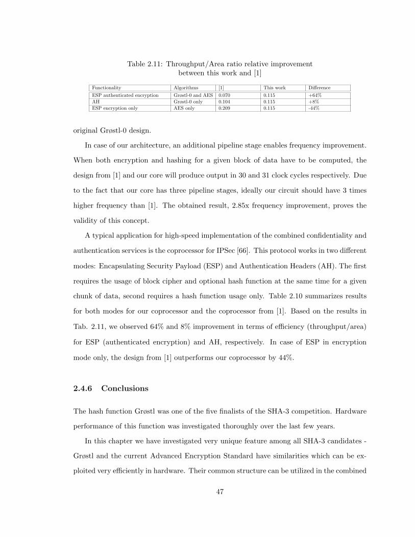
Table 2.11: Throughput/Area ratio relative improvementbetween this work and [1]
Functionality Algorithms [1] This work Difference
ESP authenticated encryption Grøstl-0 and AES 0.070 0.115 +64%
AH Grøstl-0 only 0.104 0.115 +8%
ESP encryption only AES only 0.209 0.115 -44%
original Grøstl-0 design.
In case of our architecture, an additional pipeline stage enables frequency improvement.
When both encryption and hashing for a given block of data have to be computed, the
design from [1] and our core will produce output in 30 and 31 clock cycles respectively. Due
to the fact that our core has three pipeline stages, ideally our circuit should have 3 times
higher frequency than [1]. The obtained result, 2.85x frequency improvement, proves the
validity of this concept.
A typical application for high-speed implementation of the combined confidentiality and
authentication services is the coprocessor for IPSec [66]. This protocol works in two different
modes: Encapsulating Security Payload (ESP) and Authentication Headers (AH). The first
requires the usage of block cipher and optional hash function at the same time for a given
chunk of data, second requires a hash function usage only. Table 2.10 summarizes results
for both modes for our coprocessor and the coprocessor from [1]. Based on the results in
Tab. 2.11, we observed 64% and 8% improvement in terms of efficiency (throughput/area)
for ESP (authenticated encryption) and AH, respectively. In case of ESP in encryption
mode only, the design from [1] outperforms our coprocessor by 44%.
2.4.6 Conclusions
The hash function Grøstl was one of the five finalists of the SHA-3 competition. Hardware
performance of this function was investigated thoroughly over the last few years.
In this chapter we have investigated very unique feature among all SHA-3 candidates -
Grøstl and the current Advanced Encryption Standard have similarities which can be ex-
ploited very efficiently in hardware. Their common structure can be utilized in the combined
47

datapath implementation. The coprocessor was optimized for high-speed implementation
of both functions, and can find a practical application to the IPSec-based secure networks.
It outperforms similar hardware accelerator proposed in [1] for both IPSec modes: IP
Encapsulating Security Payload (ESP) and Authentication Headers (AH) by 64% and 8%,
respectively. In case of the relatively rare, the ESP’s encryption mode only, the coprocessor
from [1] is better by 44% as compared to our results.
The fully functional HMAC-Grøstl with AES-CTR hardware accelerator compared to
the stand-alone quasi-pipelined architecture of Grøstl, described in [21] and improved in
[39], pays the price in terms of the throughput and area on all reported devices. In case of
selected Altera devices and Xilinx Virtex-6, they are up to 40% for both area and throughput
for both Grøstl-256/AES-128 and Grøstl-512/AES-256 configurations.
From our point of view, the main advantage of Grøstl, apart of its excellent hardware
and software implementation results, is the fact that the relatively small overhead in its
hardware architecture enables a natural adoption of the most important to date block
cipher - the Advanced Encryption Standard at two security levels 128 and 256-bit. As a
result, our solution can provide efficient hardware acceleration for authenticated encryption
used in multiple commercial applications.
48

Part II
Hardware architectures for public
key cryptography
49

Chapter 3: FPGA-oriented adder for thousand bits and more
In this chapter a novel, low latency, FPGA-optimized, adder has been proposed. It
efficiently combines the ideas of high-radix carry save addition and the parallel prefix
network. We have demonstrated in this chapter that this idea is especially attractive
once a modular addition is employed. The implementation results reveal that this hy-
brid adders have great potential for the addition and modular addition of the long-size
integers.
Contents
3.1 Introduction . . . . . . . . . . . . . . . . . . . . . . . . . . . . . . 50
3.2 Previous work . . . . . . . . . . . . . . . . . . . . . . . . . . . . . 52
3.3 The adder . . . . . . . . . . . . . . . . . . . . . . . . . . . . . . . . 54
3.4 Parameters selection . . . . . . . . . . . . . . . . . . . . . . . . . 61
3.5 Results discussion . . . . . . . . . . . . . . . . . . . . . . . . . . . 66
3.6 Conclusion . . . . . . . . . . . . . . . . . . . . . . . . . . . . . . . 68
3.1 Introduction
Adders are one of the most important digital circuits. They are used extensively in vari-
ous branches of science and engineering, such as digital signal processing algorithms [100],
computer graphics [101], [102] and cryptography [103], [104].
Multiple adder-based solutions have already been proposed, investigated and optimized
for different scenarios.
50
Addition can also serve as a basic building block of some higher level arithmetic opera-
tions: multiplication, modular addition, and modular multiplication.
For example: Montgomery arithmetic [105], arguably the most common concept in the
area of modular arithmetic, can be stripped down to three basic operations: a right shift,
a least significant bit comparison, and a conditional sum. Since iterative algorithms offer a
good tradeoff between computation time and circuit area, they have received considerable
attention [106], [107], [108].
Several researchers proposed the utilization of carry save adders (e.g.: [109]) for this
algorithm. The major advantages of a hardware architecture based on such adders are: the
smallest computational latency and the fact that the time complexity is constant, regardless
of the size of arguments. The biggest disadvantage of the carry save adder is the fact that its
result is in a redundant form. In order to conduct operations like a comparison or a modular
multiplication on such representation of arguments, a conversion to the non-redundant form
has to be conducted.
Moreover, Montgomery arithmetic requires also pre- and post-processing and is of in-
terest when a large number of consecutive modular multiplications is required.
This condition is easily fulfilled in case of the two oldest and most popular asymmetric,
cryptographic algorithms: RSA [24] and the Diffie-Hellman [23] scheme.
However, compared with them, the alternative public key cryptosystems, like Elliptic
Curve Cryptography [110], [111] or Pairing Based Cryptography [112] demonstrate much
more irregularities in the scheduling of basic operations. Namely, a single iteration requires
several modular additions, subtractions and multiplications.
Therefore, these cryptosystems are more computationally demanding and the efficient
hardware architectures for both modular multiplication and addition/subtraction are equally
important.
Contribution: In this effort we are going to demonstrate a novel, FPGA-optimized
adder, highly applicable for the addition of very long integers. Major contributions of this
chapter cover three different aspects and they are highlighted here:
51

• It provides a space exploration of the optimal design parameters for the fully combi-
national version of our adder.
• The proposed design provides the best results in terms of area · latency for 1024, 2048
and 4096-bit addition.
• Finally, this chapter presents, to the best of our knowledge the fastest and the most
efficient, non-redundant, modular adder (possibly subtractor), based on the novel
adder.
The rest of this chapter is organized as follows:
In Section 3.2 we discuss previous work. Section 3.3 is devoted to the description of
the proposed adder. Section 3.4 demonstrates the design rationale behind the parameters
selection. Section 3.5 discusses and analyzes the results, finally we draw conclusions in
Section 3.6.
3.2 Previous work
In order to build efficient hardware architectures for modular arithmetic, optimized for low
latency, an addition for full size arguments has to be utilized rather than any iterative
approach. The most promising, in that respect, is the carry save adder introduced in [113].
A result of addition in case of both aforementioned adders is represented in the form of
two vectors: sums and carries. To obtain the final result, both vectors have to be added.
This carry save addition is especially attractive if the last operation can be conducted
once, at the end of a sequence of multiple consecutive additions in a carry save form. An
example of application for such scenario is the Montgomery multiplication, introduced in
[105]. The fastest to date, a Montgomery multiplication hardware architecture for ASIC-
like solutions (no special multiplication enhancing resources like DSP blocks) is based on
carry save adders, as described in [109].
52

GP GPGPg ,p6 6g ,p7 7 g ,p0 0
x7 x7 y6 y0x0x6
2
1
p0
p1p
7S S Sc
8
s1
s7
s0
0
3
C C C C C C C
C C C C C C
C C C C
2(c) Kogge−Stone PPN
C C C
C C
C
C
C C C
C
2(b) Brent−Kung PPNParallel Prefix Network
(a)
Figure 3.1: (a) General concept of the parallel prefix addition, (b) Brent-Kung adder, (c)Kogge-Stone adder. GP: gi = xi · yi, pi = xi ⊕ yi, S: si = pi ⊕ ci,
: g = g′′ + g′ · p′′, p = p′ · p′′
53

However, in case of ECC algorithms where addition operations are interleaved with other
operations, like multiplications [114], the direct usage of carry save form is very challenging.
A high-radix carry-save addition, and its application to the modular multiplication of
large operands on Field-Programmable Gate Arrays (FPGAs), was introduced in [115]. The
major advantage of the high radix carry save representation over the basic radix-2 form is
the possibility of utilization of hardwired fast carry chain adders available in modern FPGA.
Moreover the carries vector, in the high radix carry save form, is relatively sparse and the
reconstruction of the final result can be simplified.
An alternative for the high radix carry save form could be one of the adders working on
full size arguments: Carry Look-Ahead adder introduced in [116], or parallel prefix network
adders, such as Brent-Kung adder [117], or Kogge-Stone adder [118]. All three of those
addition algorithms consist of three operational phases: first, the generate and propagate
flags are calculated (Fig.: 3.1 pt. 1), then the projected carries are computed (Fig.: 3.1 pt.
2), and finally, the intermediate sums are added with the projected carries (Fig.: 3.1 pt. 3).
The time complexity of the carry signal generation in Kogge-Stone adder is O(log n). It
is widely considered the fastest adder design possible. The Brent-Kung adder is expected
to be slightly slower, but also a much cheaper alternative. A ripple carry adder, based on
the hardwired fast carry chain, available in modern FPGA, has the best efficiency (area ·
latency) for relatively short arguments (less than 100-bits).
3.3 The adder
In this section we will demonstrate a hybrid high-radix carry save adder with the carry
projection unit based on parallel prefix network. First of all, the hybrid adder is taking two
arguments: A and B, and it is computing in non-redundant form the result - R, and the
output carry - cout.
This circuit can be described using two parameters: n and w. They represent the size
of arguments and the word size, respectively. The number of words in this case is denoted
54

High−Radix Carry Save Form
=1..1?
s(w−1), ..., s(0)
r(w−1), ..., r(0)
c(w)
b(w−1), ..., b(0)
a(w−1), ..., a(0)
c(2*w)
=1..1?
0 − i consecutive zerosi
C = {c(N*w), 0 , c((N−1)*w), 0 ... c(w), 0 }w−1 w−1 w
1
2
3
4
1
1
w+1
w
w
w
cout
1
1
c(N*w) c((N−1)*w)
p(N−1)
pc(N−1)
r(N*w−1)..r(N*(w−1))
Functionality: A + B = S + C = cout, R
b(N*w−1)..b(N*(w−1))
s(N*w−1)..s(N*(w−1))
a(N*w−1)..a(N*(w−1))
block N−1
g(N−2)g(N−1)
pc(N)
g(0)
block 0block 1
s(2*w−1)..s(w)
p(1)
ww
r(2*w−1), ..., r(w)
w
pc(1)
g(1)
b(2*w−1)..b(w)
a(2*w−1)..a(w) A = {a(N*w−1), ..., a(0)}
B = {b(N*w−1), ..., b(0)}
R = {r(N*w−1), ..., r(0)}
S = {s(N*w−1), ..., s(0)}
pc(N−1)
pc(N)
pc(1)
g(N−1) g(0)g(1)
p(N−1) p(1)
Parallel Prefix Network
Design X
Carry Projection Unit
Design I: Kogge−Stone PPN
Design II: Brent−Kung PPN
Flag Generation
Projected Carry Addition
Figure 3.2: Hybrid radix-2w carry save adder with the carry projection unit based onparallel prefix network (PPN). Design X - Design I is based on Kogge-Stone PPN and
Design II is based on Brent-Kung PPN
55

as N = d nwe.
The block diagram of our novel adder is shown in Fig. 3.2.
The words of A and B are added independently using the hardwired fast carry chain
adders, available in modern FPGAs. The result of this operation is in radix 2w carry save
form, and it consists of a vector of sums S = {[s((N ·w−1), ..., s((N−1) ·w)], ..., [s(w−1)...
s(0)]}, and sparse carry vector C = {c(N ·w), [0, ..., 0, c((N − 1) ·w)], ..., [0, ...0, c(w)], [0,
0, ..., 0, 0]} (Fig. 3.2 pt. 1).
For the sake of the transition of the final result in the redundant form into the non-
redundant form, several observations have to be made:
• the regular addition (ripple carry like) of both vectors, S and C, results in a non-
redundant form. This simple approach, although functionally correct, would not let
us take any advantage of the sparsity of the vector C.
• The computation of the final result in a non-redundant form can be conducted by
the iterative addition of corresponding words c(i) and s(i), from the least to the most
significant side of both vectors.
An alternative solution for this problem is the utilization of a parallel prefix network.
First, the intermediate result have to be described by two sets of flags (Fig. 3.2 pt. 2):
• propagate flags, defined by:
p(i) =
1, if s(w · (i+ 1)− 1...w · i) = (1..1)w
0, otherwise
(3.1)
• generate flags (carries), defined by:
56

g(i) =
1, if c(w · (i+ 1)) = 1
0, otherwise
(3.2)
where w - word size, N - number of words, and i ∈ ((N − 1), ..., 0). Additionally,
p(N) = 0 and g(N) = c(w ·N).
Once, all the propagate-generate signals are computed, a carry projection unit from
either Kogge-Stone [118] (Fig.: 3.1 (c)) or Brent-Kung [117] (Fig.: 3.1 (b)) adder, namely,
the parallel prefix network, can start the computations of the projected carries PC =
pc(N), ..., pc(0) (Fig. 3.2 pt. 3).
These carries are eventually added with the corresponding words from the vector of
sums (Fig. 3.2 pt. 4). This last chain of independent adders works without carries out and
the concatenation of all partial, final results from them, constitutes the final output R.
The hybrid high-radix carry save and parallel prefix network adder will be called Design
I or II based on the carry projection unit derived from either Kogge-Stone or Brent-Kung
adder, respectively.
The total delay tA of the adder is a sum of the delays of three building layers:
• flag generation, a delay of a comparator - tG,
• carry projection unit, delay of the parallel prefix network - tP ,
• projected carry addition, delay of a ripple carry adder - tC .
Therefore, the theoretical latency formula for the hybrid adder:
tA ≈ tG + tP + tC (3.3)
The formula 3.3 is going to be clarified, once we investigate how the generation of both
flags generation is implemented in modern FPGA devices (Fig. 3.3). The comparison with
57

s(3)
LUT
0
1
b(1)a(1)a(2) b(2)a(3) b(3)
p
g
s(3) s(2) s(0)s(1)
s(0)s(1)s(2)
LUT
0
1
0
1
LUT
0
1
0
1
LUT
0
1
0
1
0
1
LUTLUTLUTLUT
a(0) b(0)a(3) b(3) a(2) b(2) a(1) b(1)
a(0) b(0)
0
1
Figure 3.3: Implementation of the generate/propagate logic using fast carry chains andLUTs of Xilinx FPGAs
all ones is somehow special, and is very different than comparisons with any other numbers.
An example of the case with w = 4-bit, shown for Xilinx FPGAs, in Fig. 3.3, provides
explanations.
Only when you do the subtraction s−1111b for unsigned numbers, then carry (the going
out of range flag) is equal to 0 only if s− 1111b ≥ 0, which is equivalent to s− 1111b = 0,
and thus, s = 1111b.
Therefore, in order to evaluate if certain word has propagate property, we can simply
do a subtraction using fast carry chains, and look at the carry flag. Due to the fact, that
the computation of the subtraction from the bottom part of Fig. 3.3 can be started once
the least significant bit of the upper part addition is completed, the flag generation time,
tG is almost the same as the time of a single addition of w-bit words, at least for relatively
large values of w.
The actual value of a latency of a ripple carry adder depends on the selection of the
word size w. On the other hand, the numerical value of a latency of parallel prefix network
is related to the number of words N .
The selection of the optimal, in terms of latency, word size w, seems to be very FPGA
58
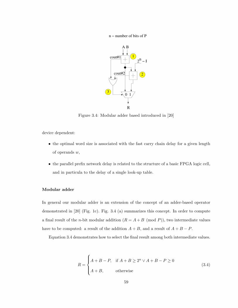
n − number of bits of P
2n
− P
1
2
30 1
A B
cout#1
cout#2
R
Figure 3.4: Modular adder based introduced in [20]
device dependent:
• the optimal word size is associated with the fast carry chain delay for a given length
of operands w,
• the parallel prefix network delay is related to the structure of a basic FPGA logic cell,
and in particula to the delay of a single look-up table.
Modular adder
In general our modular adder is an extension of the concept of an adder-based operator
demonstrated in [20] (Fig. 1c). Fig. 3.4 (a) summarizes this concept. In order to compute
a final result of the n-bit modular addition (R = A+B (mod P )), two intermediate values
have to be computed: a result of the addition A+B, and a result of A+B − P .
Equation 3.4 demonstrates how to select the final result among both intermediate values.
R =
A+B − P, if A+B ≥ 2n ∨A+B − P ≥ 0
A+B, otherwise
(3.4)
59

w
="1...1"?="1...1"?
="1...1"?="1...1"?
fpc(N)
spc(N)
Carry Projection
Unit #1
fpc(N−1)fpc(N)
fp(1)
fp(N−1)
fg(N−1)
fpc(1)
fg(0)
Unit #2
Carry Projection
spc(1)
sp(N−1)
sg(N−1)
spc(N−1)spc(N)
sg(0)
sp(1)
1
2
3
4
5
1
1
1
1
1
1
b(1)a(1)
w
w+1PE#1
c(2) 1
1
r(1)
fpc(1)
spc(1)
sel
a(0) b(0)
w
w+1PE#0
c(1)
w
w
w+1
a(N−1) b(N−1)
PE#(N−1)
r(N−1)
spc(N−1)
fpc(N−1)
c(N−1)
w fg(0)fg(1)fg(N−1)
sg(0)sg(1)sg(N−1)
fp(1)fp(N−1)
sp(N−1)
sp(1)
Functionality: (A + B) mod P = R
0 1
0 1 0 1
0 1
0 1
r(0)
sel
selsel
A = {a(N−1), ..., a(0)}, B = {b(N−1), ..., b(0)}, P = {p(N−1), ... p(0)}
wwwp(N−1) p(1) p(0)
w w
Figure 3.5: Modular adder based on the hybrid adder
Both additions in Fig. 3.4 pt. 1 and 2 can be implemented using any type of non-
redundant adder: ripple carry, Kogge-Stone, Brent-Kung, and many others. The biggest
advantage of the utilization of the hybrid adder in such application is the fact that the
computations of the second addition can be started just after the very first phase, the high
radix carry save addition, of the A + B addition has been completed (Fig. 3.5). The
computations of next two phases can be conducted in parallel. Once the condition for the
select signal for the output multiplexer is completed, it is possible to determine which path
is going to contribute to the final result of the modular addition.
Taking into account that the flag generation is conducted along with high-radix carry
save addition the latency formula of the entire circuit can be approximated as
tA ≈ 2 · tG + tP + tC . (3.5)
60

out
SIPO
ADDER
SIPO
1
2
PISO
m
3
4
in
n
m
nnn
SIPO
n
Figure 3.6: Test circuit for addition and modular addition
3.4 Parameters selection
In order to select the optimal parameters: word size - w, and the corresponding number
of words N , for a given size of arguments, a simple experiment, specific to a given FPGA
device, has to be conducted.
First of all, due to the fact that that our hybrid adder bridges the gap between two
different type of adders: ripple carry and the parallel prefix adder, we have to find the
latency characteristics of these basic adders, for different argument sizes.
Concerning two facts: limited number of pins and the delay of I/O blocks influence
on the latency of any combinational circuit, we propose to use a test circuit, presented in
Fig. 3.6. This figure demonstrates the combinational adder (Fig. 3.6 pt. 2) surrounded by
buffers: serial input parallel output (SIPO) for the input arguments, output register (Fig.
3.6 pt. 3) and parallel input serial output (PISO) for the result of the addition (Fig. 3.6 pt.
4). Thanks to such a configuration, the critical path is ensured to be in the adder circuit
itself. Moreover, in case of modular addition an extra buffer for the modulus is needed (Fig.
3.6 pt. 1).
Since the hybrid adder described in Section 3.3 consists of ripple carry adder and the
basic elements of parallel prefix network adders, then the analysis of the latency of those
61

Table 3.1: Latency of the three major addition techniques as a function of the size ofarguments
size Ripple Carry Kogge-Stone Brent-Kung
tRCA [ns] tKS [ns] tBK [ns]
Altera Cyclone III (ep3c120f780c7)
4 4.00 4.00 4.00
8 4.00 4.00 4.00
16 4.00 4.00 4.00
32 4.00 4.00 4.73
64 5.29 5.01 5.57
128 9.09 6.09 6.45
256 16.43 7.52 8.20
512 31.28 9.26 10.07
1024 N/A1 10.67 12.32
Altera Stratix III (ep3sl150f1152c2)
4 1.37 1.37 1.37
8 1.37 1.49 1.50
16 1.37 1.86 1.95
32 1.94 2.26 2.07
64 2.86 2.84 2.77
128 5.01 3.56 3.25
256 9.09 4.21 4.02
512 15.54 5.02 4.69
1024 N/A1 5.90 5.52
Xilinx Spartan 6 (xc6slx150fgg900-3)
4 1.77 1.91 1.91
8 2.11 2.79 2.63
16 2.49 3.12 3.36
32 2.57 4.13 4.03
64 3.45 5.39 4.64
128 4.83 6.53 6.08
256 7.48 7.61 6.90
512 N/A1 9.80 8.25
1024 N/A1 10.35
Xilinx Virtex 5 (xc5vlx155tff1738-3)
4 1.10 1.14 1.15
8 1.64 1.70 1.57
16 1.80 2.13 2.14
32 2.16 2.95 2.68
64 2.85 3.29 3.20
128 4.16 4.20 3.89
256 6.91 5.05 5.66
512 14.13 6.22 7.40
1024 28.20 7.79 8.201 did not fit
62

Table 3.2: Parameters exploration for the 1024-bit addition
(w,N) latency area latency · area
Altera Cyclone III (ep3c120f780c7)
[ns] [LE] [ns · LE]
Design I (8, 128) 10.67 4943 52.7
Design I (16, 64) 10.63 3977 42.3
Design I (32, 32) 12.18 3897 47.5
Design I (64, 16) 15.34 3904 59.9
Design II (8, 128) 14.39 3722 53.6
Design II (16, 64) 12.49 3565 44.5
Design II (32, 32) 13.50 3862 52.1
Design II (64, 16) 17.79 3901 69.4
Altera Stratix III (ep3sl150f1152c2)
[ns] [ALUT] [ns · ALUT]
Design I (8, 128) 6.54 3766 24.6
Design I (16, 64) 6.42 3018 19.3
Design I (32, 32) 7.17 2586 18.5
Design I (64, 16) 8.35 2328 19.4
Design II (8, 128) 6.15 2711 16.7
Design II (16, 64) 6.14 2510 15.4
Design II (32, 32) 7.12 2377 16.9
Design II (64, 16) 8.48 2268 19.2
Xilinx Spartan 6 (xc6slx150fgg900-3)
[ns] [slice] [ns · slice]
Design I (8, 128) 12.77 1893 24.2
Design I (16, 64) 12.66 1304 16.5
Design I (32, 32) 12.89 1187 15.3
Design I (64, 16) 12.92 1091 14.1
Design II (8, 128) 13.58 1456 19.8
Design II (16, 64) 14.27 1173 16.7
Design II (32, 32) 13.45 1188 16.0
Design II (64, 16) 14.49 1090 15.8
Xilinx Virtex 5 (xc5vlx155tff1738-3)
[ns] [slice] [ns · slice]
Design I (8, 128) 9.91 1655 16.4
Design I (16, 64) 10.12 1358 13.7
Design I (32, 32) 9.79 1139 11.2
Design I (64, 16) 9.90 1084 10.7
Design II (8, 128) 12.02 1366 16.4
Design II (16, 64) 10.96 1169 12.8
Design II (32, 32) 9.81 1169 11.5
Design II (64, 16) 12.90 1159 15.0
63

Table 3.3: Parameters exploration for the 1024-bit modular addition
(w,N) latency area latency · area
Altera Cyclone III (ep3c120f780c7)
[ns] [LE] [ns · LE]
Design I (8, 128) 15.91 10253 163.1
Design I (16, 64) 15.87 8324 132.1
Design I (32, 32) 18.67 7596 141.8
Design I (64, 16) 22.80 7362 167.9
Design II (8, 128) 16.93 8700 147.3
Design II (16, 64) 16.93 7464 126.4
Design II (32, 32) 19.22 7250 139.3
Design II (64, 16) 23.61 7104 167.7
Altera Stratix III (ep3sl150f1152c2)
[ns] [ALUT] [ns · ALUT]
Design I (8, 128) 9.75 6655 64.9
Design I (16, 64) 9.71 4916 47.7
Design I (32, 32) 10.37 4106 42.6
Design I (64, 16) 13.17 3672 48.4
Design II (8, 128) 9.87 4666 46.1
Design II (16, 64) 9.80 4122 40.4
Design II (32, 32) 10.38 3790 39.3
Design II (64, 16) 12.91 3509 45.3
Xilinx Spartan 6 (xc6slx150fgg900-3)
[ns] [slice] [ns · slice]
Design I (8, 128) 16.51 2742 45.3
Design I (16, 64) 23.73 1889 44.8
Design I (32, 32) 16.10 1794 28.9
Design I (64, 16) 17.83 1515 27.0
Design II (8, 128) 19.15 2761 52.9
Design II (16, 64) 17.80 1853 33.0
Design II (32, 32) 17.99 1573 28.3
Design II (64, 16) 19.34 1489 28.8
Xilinx Virtex 5 (xc5vlx155tff1738-3)
[ns] [slice] [ns · slice]
Design I (8, 128) 11.44 2932 33.5
Design I (16, 64) 11.39 2037 23.2
Design I (32, 32) 11.07 2075 23.0
Design I (64, 16) 11.61 1803 20.9
Design II (8, 128) 14.38 2579 37.1
Design II (16, 64) 13.18 1580 20.8
Design II (32, 32) 13.81 1807 25.0
Design II (64, 16) 13.63 1696 23.1
64

adders have to be conducted.
All aforementioned adders have been plugged into our test circuit. Finally, they were
implemented on two high performance FPGA devices: 65nm Altera Stratix III and Xilinx
Virtex 5, and two low cost 65nm Altera Cyclone III and 45nm Xilinx Spartan 6. All
architectures have been modeled in VHDL-93, then synthesized, placed and routed using
Xilinx ISE 13.1 and Altera Quartus II 11.1 for Xilinx and Altera FPGAs, respectively.
Maximum clock frequencies have been determined using static timing analysis tools
provided as a part of the respective software packages (quartus sta for Altera and trace for
Xilinx).
The generation of a large number of results was facilitated by an open source benchmark-
ing environment, called ATHENa (Automated Tool for Hardware EvaluatioN), developed
at George Mason University [38].
Based on the results collected in Tab. 3.1, the ripple carry addition seems to be the best
choice, in terms of latency, for argument’s sizes: up to 32-bits and 64-bits for Altera and
Xilinx devices, respectively. However, in the case of addition for arguments in the range of
1024-bit arguments, very often the FPGA tools are not even able to complete the placement
and routing successfully.
For such big precision of arguments the parallel prefix network-based adders were sig-
nificantly outperforming ripple carry adder. Surprisingly, in case of the selected FPGA
devices, the Kogge-Stone adder is not always faster than the Brent-Kung adder. In fact,
the Kogge-Stone adder, only in case of Altera Cyclone III, is clearly superior to the Brent-
Kung adder. For all other selected devices, both parallel prefix network-based adders report
implementation result differences within 10% range. The Brent-Kung adder has a marginal
advantage in Xilinx Spartax 6 and Altera Stratix III and the Kogge-Stone is slightly faster
on Xilinx Virtex 5. This surprising outcome was a result of much higher routing delays in
the case of Kogge-Stone addition.
Tables 3.2 and 3.3 summarize the result of practical search for optimal values of the
word size w for 1024-bit addition and modular addition, respectively.
65
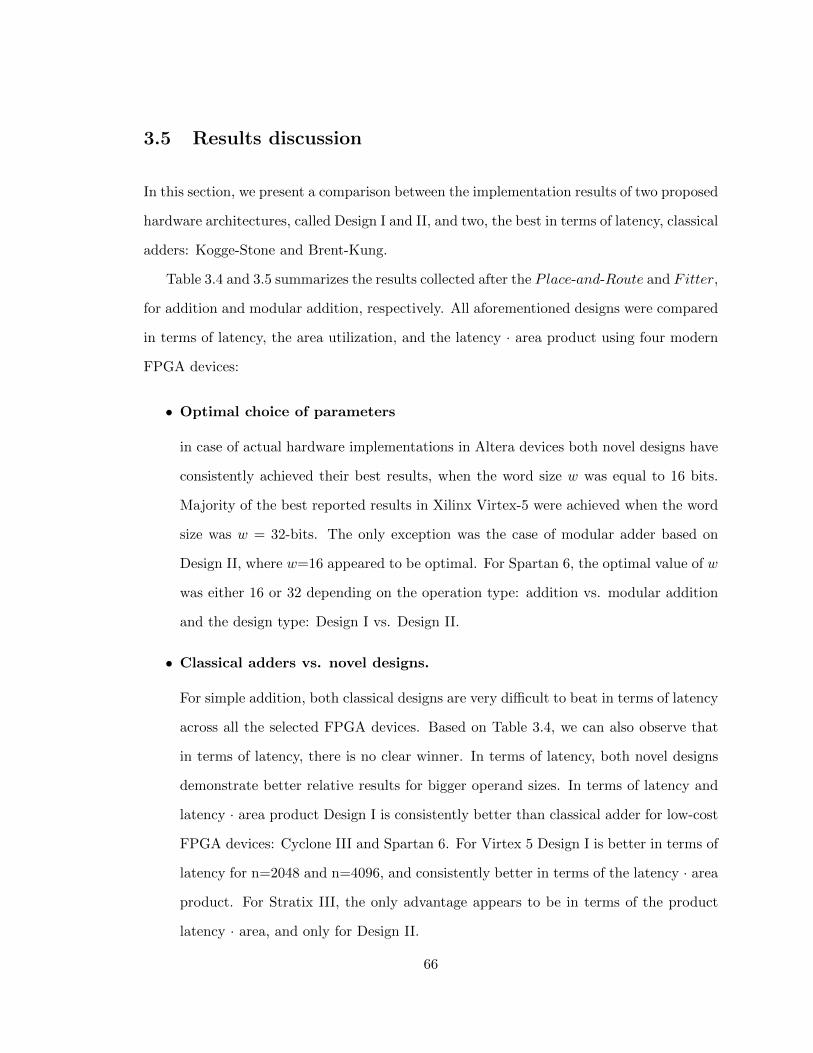
3.5 Results discussion
In this section, we present a comparison between the implementation results of two proposed
hardware architectures, called Design I and II, and two, the best in terms of latency, classical
adders: Kogge-Stone and Brent-Kung.
Table 3.4 and 3.5 summarizes the results collected after the Place-and-Route and Fitter,
for addition and modular addition, respectively. All aforementioned designs were compared
in terms of latency, the area utilization, and the latency · area product using four modern
FPGA devices:
• Optimal choice of parameters
in case of actual hardware implementations in Altera devices both novel designs have
consistently achieved their best results, when the word size w was equal to 16 bits.
Majority of the best reported results in Xilinx Virtex-5 were achieved when the word
size was w = 32-bits. The only exception was the case of modular adder based on
Design II, where w=16 appeared to be optimal. For Spartan 6, the optimal value of w
was either 16 or 32 depending on the operation type: addition vs. modular addition
and the design type: Design I vs. Design II.
• Classical adders vs. novel designs.
For simple addition, both classical designs are very difficult to beat in terms of latency
across all the selected FPGA devices. Based on Table 3.4, we can also observe that
in terms of latency, there is no clear winner. In terms of latency, both novel designs
demonstrate better relative results for bigger operand sizes. In terms of latency and
latency · area product Design I is consistently better than classical adder for low-cost
FPGA devices: Cyclone III and Spartan 6. For Virtex 5 Design I is better in terms of
latency for n=2048 and n=4096, and consistently better in terms of the latency · area
product. For Stratix III, the only advantage appears to be in terms of the product
latency · area, and only for Design II.
66

Table 3.4: Implementation results for combinational versions of selected adders in the1024-4096-bit range. ∆ latency, ∆ area, ∆ latency · area - relative change in comparison
to the best of the two classical designs in terms of latency, area and latency · areaproduct, respectively.
size adder (w, N) latency area latency · area ∆ latency ∆ area ∆ latency · area
[ns] [LE /ALUT /slice] [ns · slices ·103] [%] [%] [%]
Altera Cyclone III (ep3c120f780c7)
1024
Kogge-Stone 10.67 18287 195.1 - - -Brent-Kung 12.32 5169 63.7 - - -
Design I (16, 64) 10.63 3977 42.3 -0.4 -23.1 -33.6Design II (16, 64) 12.49 3565 44.5 +17.5 -31.0 -30.1
2048
Kogge-Stone 14.33 45618 653.8 - - -Brent-Kung 14.46 10415 150.6 - - -
Design I (16, 128) 12.22 8239 100.7 -14.7 -20.9 -33.2Design II (16, 128) 13.84 7121 98.6 -3.4 -31.6 -26.3
4096
Kogge-Stone N/A N/A N/A N/A N/A N/ABrent-Kung 18.55 20986 389.4 - - -
Design I (16, 256) 14.59 17095 249.4 -21.4 -18.5 -35.9Design II (16, 256) 16.56 15591 258.2 -10.7 -25.7 -33.7
Altera Stratix III (ep3sl150f1152c2)
1024
Kogge-Stone 5.90 17238 101.7 - - -Brent-Kung 5.52 3091 17.1 - - -
Design I (16, 64) 6.42 3018 19.4 +16.2 -2.4 +13.5Design II (16, 64) 6.14 2510 15.4 +11.2 -18.8 -9.7
2048
Kogge-Stone 7.38 39188 289.1 - - -Brent-Kung 6.34 6299 39.9 - - -
Design I (16, 128) 7.32 6361 46.6 +15.4 +1.0 +16.6Design II (16, 128) 6.72 5054 34.0 +6.0 -19.8 -15.0
4096
Kogge-Stone 9.77 88328 862.8 - - -Brent-Kung 7.39 12813 94.7 - - -
Design I (16, 256) 8.31 13420 111.5 +12.4 +4.7 +17.7Design II (16, 256) 8.02 10130 81.3 +8.5 -20.9 -14.2
Xilinx Spartan 6 (xc6slx150fgg900-3)
1024
Kogge-Stone 17.84 4511 80.5 - - -Brent-Kung 12.71 1898 24.1 - - -
Design I (16, 64) 12.66 1304 16.5 -0.4 -31.3 -31.6Design II (32, 32) 13.45 1188 16.0 +5.7 -37.4 -33.8
2048
Kogge-Stone 25.51 10780 275.0 - - -Brent-Kung 15.55 3703 57.6 - - -
Design I (16, 128) 14.78 2548 37.7 -5.0 -31.2 -34.6Design II (32, 64) 15.45 2297 35.5 -0.6 -38.0 -38.4
4096
Kogge-Stone 31.40 21097 662.3 - - -Brent-Kung 21.57 5258 113.4 - - -
Design I (64, 64) 17.96 4193 75.3 -16.8 -20.3 -33.6Design II (16, 256) 19.32 4311 83.3 -10.4 -18.0 -26.6
Xilinx Virtex 5 (xc5vlx155tff1738-3)
1024
Kogge-Stone 7.79 4476 34.9 - - -Brent-Kung 8.20 1988 22.4 - - -
Design I (32, 32) 9.79 1100 10.8 +25.7 -44.7 -52.0Design II (32, 32) 9.81 1169 11.5 +25.9 -41.2 -48.9
2048
Kogge-Stone 18.05 9699 175.1 - - -Brent-Kung 10.98 3545 38.9 - - -
Design I (32, 64) 9.93 2707 26.9 -9.5 -23.6 -30.9Design II (32, 64) 11.77 2046 24.1 +7.3 -42.3 -38.1
4096
Kogge-Stone 25.55 19677 502.7 - - -Brent-Kung 13.08 5099 66.7 - - -
Design I (32, 128) 12.71 4696 59.7 -2.8 -7.9 -10.5Design II (32, 128) 13.34 3749 50.0 +2.0 -26.4 -25.0
67
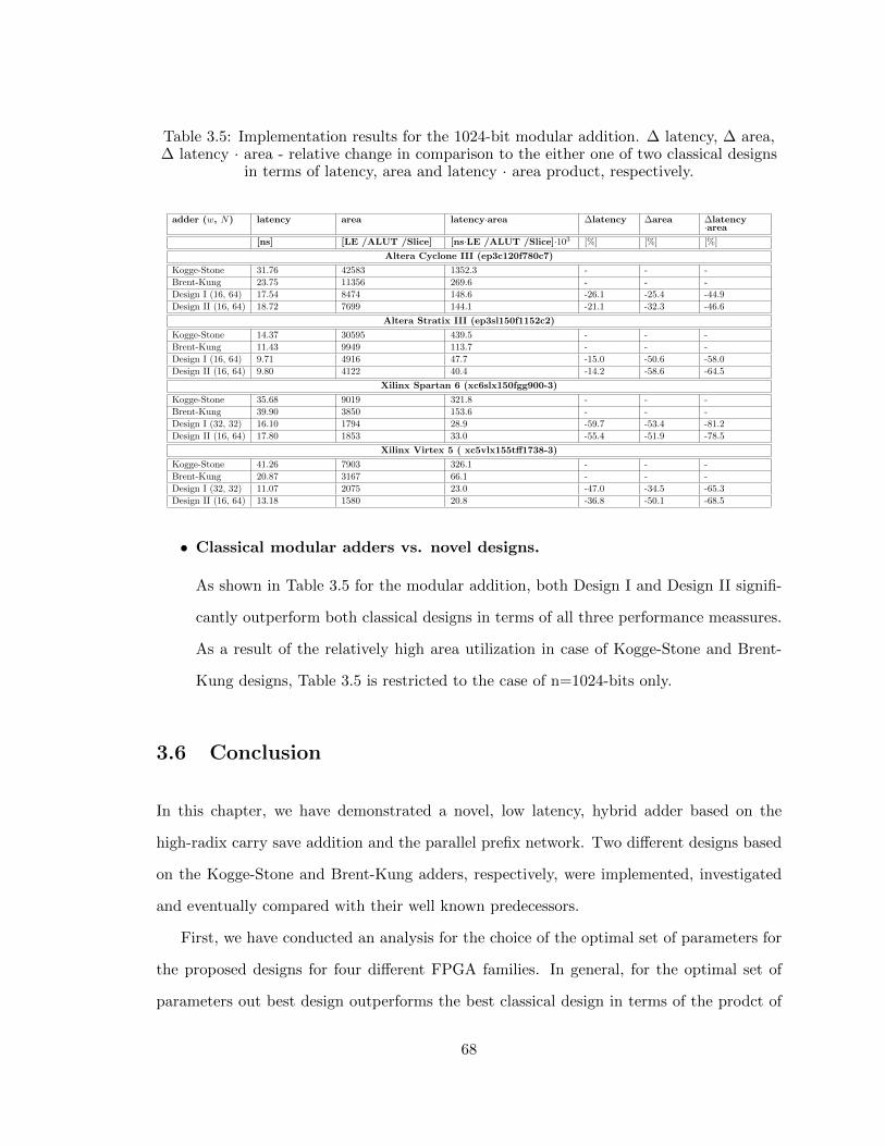
Table 3.5: Implementation results for the 1024-bit modular addition. ∆ latency, ∆ area,∆ latency · area - relative change in comparison to the either one of two classical designs
in terms of latency, area and latency · area product, respectively.
adder (w, N) latency area latency·area ∆latency ∆area ∆latency·area
[ns] [LE /ALUT /Slice] [ns·LE /ALUT /Slice]·103 [%] [%] [%]
Altera Cyclone III (ep3c120f780c7)
Kogge-Stone 31.76 42583 1352.3 - - -
Brent-Kung 23.75 11356 269.6 - - -
Design I (16, 64) 17.54 8474 148.6 -26.1 -25.4 -44.9
Design II (16, 64) 18.72 7699 144.1 -21.1 -32.3 -46.6
Altera Stratix III (ep3sl150f1152c2)
Kogge-Stone 14.37 30595 439.5 - - -
Brent-Kung 11.43 9949 113.7 - - -
Design I (16, 64) 9.71 4916 47.7 -15.0 -50.6 -58.0
Design II (16, 64) 9.80 4122 40.4 -14.2 -58.6 -64.5
Xilinx Spartan 6 (xc6slx150fgg900-3)
Kogge-Stone 35.68 9019 321.8 - - -
Brent-Kung 39.90 3850 153.6 - - -
Design I (32, 32) 16.10 1794 28.9 -59.7 -53.4 -81.2
Design II (16, 64) 17.80 1853 33.0 -55.4 -51.9 -78.5
Xilinx Virtex 5 ( xc5vlx155tff1738-3)
Kogge-Stone 41.26 7903 326.1 - - -
Brent-Kung 20.87 3167 66.1 - - -
Design I (32, 32) 11.07 2075 23.0 -47.0 -34.5 -65.3
Design II (16, 64) 13.18 1580 20.8 -36.8 -50.1 -68.5
• Classical modular adders vs. novel designs.
As shown in Table 3.5 for the modular addition, both Design I and Design II signifi-
cantly outperform both classical designs in terms of all three performance meassures.
As a result of the relatively high area utilization in case of Kogge-Stone and Brent-
Kung designs, Table 3.5 is restricted to the case of n=1024-bits only.
3.6 Conclusion
In this chapter, we have demonstrated a novel, low latency, hybrid adder based on the
high-radix carry save addition and the parallel prefix network. Two different designs based
on the Kogge-Stone and Brent-Kung adders, respectively, were implemented, investigated
and eventually compared with their well known predecessors.
First, we have conducted an analysis for the choice of the optimal set of parameters for
the proposed designs for four different FPGA families. In general, for the optimal set of
parameters out best design outperforms the best classical design in terms of the prodct of
68

latency · area for all four investigated families. Due to this fact the latency · area, for the
selected argument sizes, is always improved in comparison to the selected benchmarks.
Moreover, our hybrid high-radix carry save adders with carry projection unit based on
parallel prefix network have been applied to the classical design of the modular addition
circuit. The implementation results on modern FPGA devices have revealed that latency,
area and latency latency · area, for Altera devices, have been improved on average 15, 40 and
55 percent, respectively. In case of Xilinx devices these average improvements amounted to
50, 45 and 70 percent, respectively.
Finally, we believe that, in order to improve the addition for a thousand bits and more
in modern FPGA devices, some changes in their internal structure could have been incorpo-
rated by vendors themselves. For example, a limited number of the parallel prefix networks
(of the size either 16, 32 or 64-bit) could be added. Similarly to DSP units, these carry
projection units based on parallel prefix networks could be configured to operate in either
combinational or pipelined mode.
For the future work we are going to investigate the application of the aforementioned
concept to the high level applications like coprocessors supporting computations of crypto-
graphic schemes based on elliptic curve and pairing transformations over primes fields.
69
Chapter 4: Hardware architectures for modular arithmetic
based on the use of Solinas numbers and heterogenous
FPGA devices
In this chapter, we demonstrate novel hardware architectures for high speed modular
arithmetic based on the use of the Solinas primes and DSP units of modern FPGAs.
Our goal is to show that combining the Barrett algorithm, the Booth recoding, and the
high-radix carry save representation of arguments enables very efficient, parallel modular
arithmetic, optimized for this important class of prime numbers.
Contents
4.1 Introduction and motivations . . . . . . . . . . . . . . . . . . . . 70
4.2 Previous work . . . . . . . . . . . . . . . . . . . . . . . . . . . . . 71
4.3 Architectures for the Solinas primes . . . . . . . . . . . . . . . . 75
4.4 Conclusions . . . . . . . . . . . . . . . . . . . . . . . . . . . . . . . 89
4.1 Introduction and motivations
A well known shortcut for modular multiplication modulo a Mersenne number (2k-1), which
amounts to performing modular reduction without integer division, has been generalized by
the National Security Agency (NSA) researcher - Jerome A. Solinas in [119]. In this work
he discussed numbers of the following form 2a±2b±2c±1, and gcd(a, b, c) = word size, and
word size = 16, 32, 64. In [119] Solinas has also demonstrated a corresponding reduction
method, based on a few additions and subtractions. A big class of Solinas prime numbers
70
and their efficient arithmetic have been widely accepted and recommended for the NIST
standard - Elliptic Curve Digital Signature Algorithm (ECDSA) [120].
The aforementioned technique is not applicable for all Solinas primes, in particular for
those primes, which are recommended for the higher security levels of pairing transforma-
tions (e.g. Solinas primes from [121] (section 7.2) or [37]).
In this chapter, we are going to demonstrate new hardware architectures for modular
addition, multi-operand addition, multiplication and reduction, optimized for the use of
Solinas primes.
The rest of this chapter is organized as follows:
In Section 4.2 we discuss relevant previous work in the area of modular multiplication
(the addition architectures has been discussed in the previous chapter). Section 4.3 is
devoted to the discussion of the hardware architectures for Solinas primes. Finally, in
Section 4.4 we conclude our work.
4.2 Previous work
In 1985 Montgomery proposed modular multiplication without trial division [105]. A novel
number representation and a novel basic arithmetic operation were named after his name
numbers in the Montgomery domain and the modular Montgomery multiplication, respec-
tively. It enables the multiplication and reduction to be conducted in parallel.
In 1999 Tenca et al. [106] proposed the first scalable architecture for Montgomery
Multiplication. Harris et al. in [107] and Huang et al. in [122] have improved this design
in terms of latency and latency · area by a factor of two.
Further improvement of the aforementioned architectures was possible when higher
radixes were introduced. They were demonstrated for the Tenca et al., Harris et al. and
Huang et al. designs in [123], [124] and [122], respectively.
Kaihara et al. in [125] proposed the BiPartite multiplication, a concept which enables
parallel execution of the Montgomery and Interleaved multiplication. Oksuzoglu et al. in
71

[126] reported DSP-based architecture for low-cost devices.
The TriPartite algorithm in [127] effectively integrates three different existing algo-
rithms, a classical modular multiplication based on Barrett reduction [128], the modular
multiplication with Montgomery reduction and the Karatsuba multiplication [129] algo-
rithms in order to reduce the computational complexity and increase the potential of parallel
processing.
Hardware architectures of modular arithmetic for parallel computing were demonstrated
using Residue Number System in [130] and Spectral Modular Arithmetic in [131] and [132].
Long integers can be multiplied modulo Solinas primes using the aforementioned Mont-
gomery arithmetic, in particular using, so called, quotient pipelining technique proposed by
Orup [133].
The Orup’s method has been been adapted by Suzuki in [134] and [135] to the DSP
block available in Xilinx Virtex-4 and Virtex-5, respectively. To the best of our knowledge,
Suzuki’s hardware architecture is the fastest to date FPGA implementation of the Mont-
gomery multiplication. Due to the internal dependencies in Orup algorithm ([134] Tab. 2),
the computations of the consecutive words of the final result is separated by the interval of
two clock cycles. Thus, the latency formula in case of Orup algorithm converges to 2 · N ,
where N denotes the number of words representing arguments.
An alternative solution is to separate both basic operations: the multiplication and
reduction, and conduct the optimization on them separately. In such approach it is possible
to introduce basic, two-stage pipelining into multiplication-reduction computations.
In case of the multiplication, several improvements have been analyzed in the past by
Karatsuba et al.[129], Toom [136], Schonhage and Strassen [137] and recently Furer [138].
All four aforementioned methods would require large amount of DSP units, thus we are
going to use simpler, conceptually slower, yet powerful, grid (also called box) multiplication
method. The latency formula in case of grid multiplication converges to N .
In case of the reduction, for a random prime number, the complexity of the classi-
cal Barrett reduction [128] is equivalent to the complexity of the multiplication method.
72

However for the meticulously selected Solinas primes this algorithm might be simplified
to few additions and subtractions. The optimization of the Barrett reduction for Solinas
primes is going to be beneficial for the scheduling of scenarios where pipelining technique
can not be utilized (e.g. an exponentiation enforces the date dependency in consecutive
multiplications).
A brief overview of hardware architectures for modular arithmetic is provided in table
4.1.
Table 4.1: General Purpose Modular Multiplication/Inversion architectures for GF(p)
Algorithm Radix-2 Higher Radix Scalability
Montgomery Multiplication
Binary Arithmetic
Tenca and Koc [106] [123] yes
Harris et al. [107] [124] yes
Huang et al. [122] [122] yes
Michalski and Buell [139] yes
McIvor et al. [109] no
Suzuki [134] yes
Oksuzoglu and Savas [126] yes
Residue Numbers Systems Arithmetic
Kawamura NA [130] no
Bajard et al. NA [140], [141] no
Spectral Modular Arithmetic
Saldamlı and Koc [131], [142] no
Baktır et al. [132] no
Interleaved Multiplication-Reduction
Amanor [143] yes
AbdelFattah et al. [144] no
Mixed Montgomery-Interleaved Multiplication
Kaihara and Takagi [125], [145] [125], [145] yes
Sakayama et al. [127] no
73

0 1 0
1 0
01
0 1
2n
− P
2n
− P
A
cout#2
cout#1
cout#1
cout#2
SUB
P
AA B
B
cout#1 cout#1
cout#2
1
R R
R
P
SUB
B
SUB
cout#1
n − number of bits of P
1
Figure 4.1: Modular adder/subtractor - high level block diagram
0 1
11
10 9
4
2
1
12
65
13
7
8
Unit #2
Carry Projection
3
80−bit: n=521−bits, N=31 words
120−bit: n=1264−bits, N=75 words
128−bit: n=1493−bits, N=88 words
w=17−bits
="1...1"?="1...1"?
="1...1"?="1...1"?
1
1
r(0)
1
1
1
1
sel
b(1)a(1)
w
w+1PE#1
c(2) 1
1
r(1)
fpc(1)
spc(1)
sel
ip(1)
p(1)
a(0) b(0) "0""1"
w
w+1PE#0
c(1)
p(0)
ip(0)
sel
Carry Projection
Unit #1
w
sel
w
w+1
w w
w
fpc(1)
wa(N−1) b(N−1)
PE#(N−1)
fpc(N)
fpc(N)
spc(N)
spc(N)spc(N−1) spc(1)
fpc(N−1)fpc(N)
r(N−1)
spc(N−1)
fpc(N−1)
ip(N−1)
p(N−1)c(N−1)
w
A = {a(N−1), ..., a(0)}, B = {b(N−1), ..., b(0)}, p = {p(N−1), ... p(0)}, ip = two’s complement of pFunctionality: (A + B) mod p = R
fg(0)fg(1)fg(N−1)
sg(0)sg(1)sg(N−1)
fp(1)fp(N−1)
sp(N−1)
sp(1)
fg(0)fp(1)fg(N−2)
fp(N−1) fp(N−2)
sp(N−1) sg(0)sp(N−2)
sg(N−2) sp(1)
subtraction
0 10 10 1
0 1 0 1 0 1
0 1
0 1
1 0
1 0
1 0
Figure 4.2: Pipelined high-radix carry save modular adder/subtractor
74

4.3 Architectures for the Solinas primes
4.3.1 Modular adder/subtractor
In general our modular adder/subtractor is an extension (Fig. 4.1) of the concept of adder-
based operator demonstrated for instance in [20] (Fig. 1c). It is demonstrated in Fig. 4.2
and it supports both modular addition or subtraction (argument B has to be transformed
into one’s complement form and ’1’ has to be added to the least significant word Fig. 4.2
pt. 1).
Both A and B as well as modulus p and its two’s complement value ip are split into N
w-bits words. First, A and B are added (or subtracted) and the intermediate result, in 2w
radix carry save form, is computed.
Those intermediate results must be stored into registers (Fig. 4.2 pt. 2). Next in line
is the addition of this partial result with either modulus or its two’s complement value for
subtraction and addition, respectively (Fig. 4.2 pt. 4), and again the intermediate results
(vector of sums and carries) of this operation are stored into registers (Fig. 4.2 pt. 5).
Both intermediate results, represented as vectors of sums and carries, have additional
sets of flags. The first and the second intermediate results produce {fp(n − 1), ..., fp(0)},
{fg(n− 1), ..., fg(0)} (Fig. 4.2 pt. 3) and {sp(n− 1), ..., sp(0)}, {sg(n− 1), ..., sg(0)} (Fig.
4.2 pt. 6), respectively.
The flag fp(i) is set when i-th word of the first intermediate result consists of all ones (Eq.
3.2). The flag fg(i) is set when the carryout from the i-th block of the first intermediate
result is equal to one. The definition of flags: sp(i), sg(i) is identical except that they
concern second intermediate result. Those flags are going to two separate carry projection
units (Fig. 4.2 pt. 7 and 8), which are described in the next subsection.
A single carry projection unit computes the projected carries within a deterministic
number of clock cycles. In order to increase the performance of the whole modular adder
additional chains of registers were added (Fig. 4.2 pt. 9 and 10), making this circuit fully
75

pipelined. The number of modular additions possible to perform at the same time for a
given security level are summarized in Table 5.6.
Finally, both carry projection units compute vectors of projected carries and also deter-
mine which intermediate result will be selected as the final result. In order to do that, we
need to investigate two separate cases for the addition (Eq. 4.1) and subtraction (Eq. 4.2).
• R = A+B (mod P )
R =
A+B − P, if A+B ≥ 2k ∨A+B − P ≥ 0
A+B, otherwise
(4.1)
• R = A−B (mod P )
R =
A−B + P, if A−B < 0
A−B, otherwise
(4.2)
In case of the addition, the conditions (A + B ≥ 2k) or (A + B − P ≥ 0) corresponds
to the values of fpc(N) and spc(N) (the most significant carries computed in the carry
projection units), respectively. If any of these conditions happens the value of A + B − P
has to be selected, otherwise the value A + B is correct. On the other hand, when the
subtraction is conducted, we have to check only if the first intermediate result is negative
or positive. Thus, evaluation of the flag fpc(N) is sufficient for the determination which
value, A−B + P or A−B, should be chosen.
Based on the aforementioned conditions, the signal sel (Fig. 4.2 pt. 13) selects one of
the partial results for the final addition with projected carries, and the final result (Fig. 4.2
pt. 11 and 12) is obtained.
76
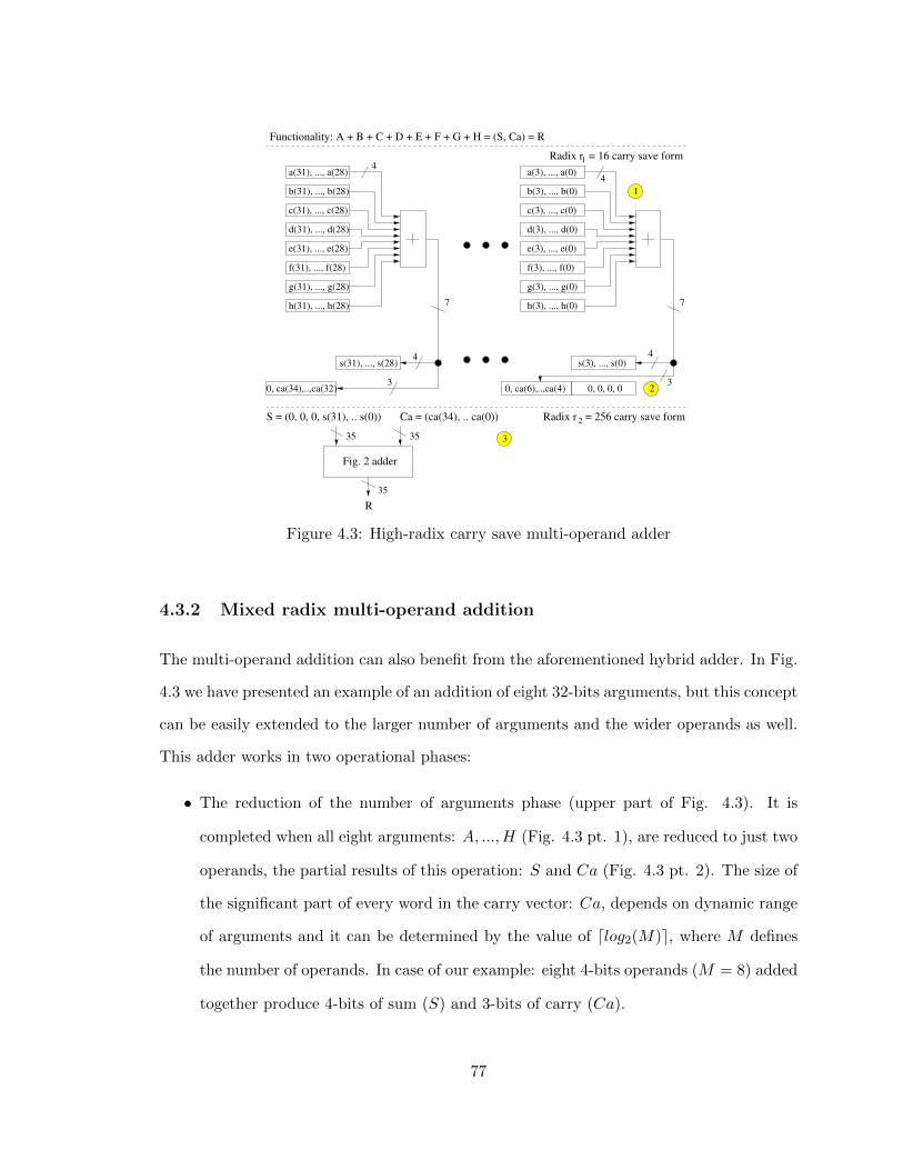
1
2
3
h(31), ..., h(28)
g(31), ..., g(28)
f(31), ..., f(28)
e(31), ..., e(28)
d(31), ..., d(28)
c(31), ..., c(28)
b(31), ..., b(28)
a(31), ..., a(28)
h(3), ..., h(0)
g(3), ..., g(0)
f(3), ..., f(0)
e(3), ..., e(0)
d(3), ..., d(0)
c(3), ..., c(0)
b(3), ..., b(0)
a(3), ..., a(0)
0, ca(6),..,ca(4) 0, 0, 0, 0
s(3), ..., s(0)
0, ca(34),..,ca(32)
s(31), ..., s(28)
Fig. 2 adder
S = (0, 0, 0, s(31), .. s(0)) Ca = (ca(34), .. ca(0))
4
7
4
3
R
35
Radix r = 256 carry save form2
Radix r = 16 carry save form1
35 35
7
4
3
4
Functionality: A + B + C + D + E + F + G + H = (S, Ca) = R
Figure 4.3: High-radix carry save multi-operand adder
4.3.2 Mixed radix multi-operand addition
The multi-operand addition can also benefit from the aforementioned hybrid adder. In Fig.
4.3 we have presented an example of an addition of eight 32-bits arguments, but this concept
can be easily extended to the larger number of arguments and the wider operands as well.
This adder works in two operational phases:
• The reduction of the number of arguments phase (upper part of Fig. 4.3). It is
completed when all eight arguments: A, ...,H (Fig. 4.3 pt. 1), are reduced to just two
operands, the partial results of this operation: S and Ca (Fig. 4.3 pt. 2). The size of
the significant part of every word in the carry vector: Ca, depends on dynamic range
of arguments and it can be determined by the value of dlog2(M)e, where M defines
the number of operands. In case of our example: eight 4-bits operands (M = 8) added
together produce 4-bits of sum (S) and 3-bits of carry (Ca).
77

• The addition of the intermediate values: (S, Ca) (lower part of Fig. 4.3 pt. 3) is
performed exactly like in case of the adder described in the previous chapter.
Due to the fact that the eight-argument addition is logically more complex than the
two-argument addition, we have decided to conduct both phases using two different radices.
The first phase radix r1 is always smaller than the second phase radix r2. In Fig. 4.3,
r1 = 24 and r2 = 28, but the optimal ratio between these two parameters seems to be
specific issue for a given FPGA family.
4.3.3 Modular multiplier with Booth recoding and Barrett reduction
4.3.4 Multiplication using DSP blocks
This circuit is based on a grid multiplication method adapted to modern FPGA structures.
In order to achieve high-speed computations, DSP slices available on modern FPGA devices,
have to be used. In this section Xilinx Virtex-6 devices will serve as a case study. Due to the
fact that every Virtex-6 DSP unit contains 17x24 multiplier, both multiplication arguments
have to be represented in two different radices (217 and 224).
Every argument can be then represented by N and M words in the respective radix.
The sizes of arguments at a given security level are summarized in Tab. 5.1. The number
of words in a particular representation can be computed using formula d nwe, where n and w
correspond to the sizes of arguments and words in bits, respectively.
The argument A (Fig. 4.4 pt. 1), represented in radix 217, is constant during the
particular multiplication. The argument B is scanned in 24-bit chunks and it is updated
every clock cycle from the least significant to the most significant word. This configuration
is optimized for low latency rather than the small DSP utilization.
Every clock cycle, every DSP block produces N (in case of 80-bit security N=31) 41-
bit chunks of intermediate data. As a consequence of a 17-bit granulation of argument A,
the neighboring 41-bit chunks contribute to the different parts of partial sum and they are
78

1
3
2
24
17Switch Radix 2
to Radix2 Carry
80−bit: N=31, M=22
120−bit: N=75, M=53
128−bit: N=88, M=62
4
DSP Slice
b(j) b(j)
17 24
41
"0"
7
7
177
1717
2
17
a(0) b(j)
s(0)
"0"
s(−1)
"0"
24
Radix 2 operations17
24Radix 2 operations
c(1)
24
s(−1)s(0)
17
24
17Switch Radix 2
to Radix2 Sum
24
zc(−1)
ss(−1)
cc(−1)
17
24
2
"0"
"0"
24
cc(−1)ss(−1)
rr(0)
2
"0"
"0"
cc(0)ss(0)
24
241 11
a(N−1) a(N−2)
zc(N)
cc(M)
s(N) c(N) s(N−1) c(N−1)s(N−2)
s(N) s(N−1)
ss(M)
ss(M) cc(M)
rr(2M−1) rr(2M−2) rr(M−1) rr(M−2)rr(M−3)
Functionality: A * B = (RR, RC), where A = {a(N−1), ..., a(0)}, B = {b(N−1_, ...,0}, RR = {rr(2M−1), ..., rr(0)}, RC = {rc(2M−1), ..., rc(0)}
rc(M−1)rc(M)rc(2M−1)rc(2M)
24
24
2
"0"24
24
1
ss(i) cc(i)
rr(i+M−1)
24
24
2
"0"24
24
1
ss(i) cc(i)
rr(i+M−1)
24
24
2
"0"24
24
1
ss(i) cc(i)
rr(i+M−1)
"0" "0" "0"
rc(i+M) rc(i+M) rc(i+M)
24
24
2
"0"
"0"24
24
1
ss(M−1) cc(M−1)
Three operational phases of the selected processing element:
Phase I: clock cycle 0 Phase II: clock cycle 1..M−2 Phase III: clock cycle M−1
....
zc(−1) = 0zc(0) = 0
zc(N−1) = 0 , c(N−1)
17
15
15
15zc(N) = 0 , c(N)
zc(1) = 0 , c(1)
17
Figure 4.4: Block diagram of a multiplier based on 24x17 DSP units
79

p(M/2−1)
PE #(0)
5 7
34
PE #(2M−1) PE #(3M/2) PE #(3M/2−1) PE #(M/2) PE #(M/2−1)
80−bit: M=44
120−bit: M=106
128−bit: M=126
Outputs from single multiplier:
RR = {rr(2M−1), ..., rr(0)}RC = {rc(2M), ..., rc(0)}
1
2
34
7
5
="1..1" ?
6
r(0)
0 0
00 00
00
g(1)
r(2M−1)
p(2M−1)
pc(2M−1)
r(3M/2)
p(3M/2)
g(3M/2+1)
pc(3M/2)
r(3M/2−1)
g(3M/2)
pc(3M/2−1)
r(M/2)
p(M/2)
g(M/2+1)
pc(M/2)
g(M/2)
pc(M/2−1)
r(M/2−1)
RR, RC
L_RR, L_RC
R_RR, R_RC
R = {r(2M−1), ..., r(0)}
Outputs from two multipliers:
L_RR = {l_rr(2M−1), ..., l_rr(0)}
R_RR = {r_rr(2M−1), ..., r_rr(0)}
Functionality: (RR, RC) = R and (L_RR, L_RC) + (R_RR, R_RC) = R
24
L_RC = {l_rc(2M), ..., l_rc(0)}
R_RC = {r_rc(2M), ..., r_rc(0)}
pc(j)
r(j)
cin(j)cout(j+1)
r_rr(j)r_rc(j)rc(j) rr(j)
PE #j
l_rc(j) l_rr(j)
2
2
241
24
2424
1 1
242
1
1
1
p(j)
g(j+1)
Unit
Carry Projection
pc(0)
p(1)p(2M−1)
pc(2M−1)
g(1)g(2M−1)
p(3M/2−1)
Figure 4.5: Additional circuit for the multiplier double speed mode support.
(L RR = (RR << 24·M2 ), L RC = (RC << 24·M
2 ), for (RR, RC) from left multiplier) and
(L RR = RR, L RC = RC, for (RR, RC) from right multiplier)
80

shifted by 17 positions to the right. In order to compute the final value of multiplication -
all partial sums must be added.
As a result of the facts: the argument A consists of N 17-bit words and only 24-bits of
argument B (b(j)) are used, then the size of the product A · b(j) is defined by 17 ·N + 24.
This lead us to the conclusion that N + 2 17-bits words are needed for the representation
of this partial product (the indices of (S, C) on Fig. 4.4 are between N and −1) .
Correspondingly, because of the 24-bit granulation of argument B, the neighboring par-
tial sums contribute to different parts of the final result and they are shifted by 24 positions
to the right (Fig. 4.4 pt. 4).
Due to the discrepancies in relative positions between 41-bit chunks of data produced
by DSPs and the relative positions between partial sums, the radix changes are introduced
(Fig. 4.4 pt. 2, pt. 3). They are implemented by simple rewiring.
However, every partial sum is represented by N + 2 17-bit words at the input to the
radix change module and it has to be transferred into M + 2 24-bits words. It is a natural
consequence of the fact that d (N+2)·1724 e represents the number of output words.
The partial result of multiplication is obtained in a high radix carry save form: a sum
vector (Fig. 4.4: RR) and a carry vector (Fig. 4.4: RC).
The numbers of clock cycles required to perform the multiplication at a given security
level are summarized in Table 5.6.
Our grid multiplier could easily benefit form the Karatsuba’s algorithm [129]. However,
the basic step of Karatsuba’s algorithm allows us to compute the product of two large
numbers A and B using three multiplications of smaller numbers, each with about half
as many digits as A or B, and also three additions and digit shifts. Therefore, the most
basic version of parallel Karatsuba approach would result with approximately 32x more DSP
units. Further recursion would provide even higher DSP block utilization, but also it would
help improve the latency of a single multiplication. In this chapter we will report result for
a multiplier without the Karatsuba trick.
81

4.3.5 Double-speed mode
A computation of a pairing transformation consists of execution of two other algorithms: the
Miller’s loop and the final exponentiation. Those algorithms demonstrate different data-
dependency schemes and due to that fact different number of basic arithmetic modules
might be optimal for them.
The major motivation behind the introduction of the double speed mode (further im-
provement is possible and it depends on the application and number of multiplication units)
for the multiplier was the fact that a single iterations of Alg. 4, Alg. 3 can be achieved using
up to four independent streams of data and a single iteration of Alg. 7 requires two modular
multiplications only. The latency-optimized design of our coprocessor (details in the next
section), conducting the Miller loop computations, requires four multipliers working in par-
allel in a basic mode. On the other hand, a single iteration of the final exponentiation need
only two multipliers working in parallel. The major motivation behind the introduction of
this special double speed mode was full utilization of computational resources and thanks
to this fact shortening the latency of a single iteration of the final exponentiation.
Kaihara and Takagi have introduced the Bipartite multiplication in [125]. This con-
cept enables splitting multiplication into two parts. These two parts are then processed
separately, in parallel, potentially doubling the speed of calculations. Later on, the Bi-
Partite multiplication was generalized using Karatsuba [129] algorithm, and the TriPartite
multiplication was introduced in [127].
A double speed mode in case of the multiplier proposed in this chapter is an idea inspired
by the aforementioned concepts, however the computations in both paths are in the same
integer domain (in [125] and [127] one of the domains is Montgomery and the other one is
natural, integer domain.). Let A,B be w ·N -bit numbers, and A = AH · 2w·N2 + AL, then
the multiplication of A and B can be computed as follows
82

A ·B = (AH · 2w·N2 +AL) ·B = AH ·B · 2
w·N2 +AL ·B. (4.3)
Both terms, AH · B and AL · B are calculated using two separate multipliers in a half
of the clock cycles. In order to complete the multiplication, an extra circuitry (Fig. 4.5) is
needed for the addition of both partial sums.
In case of normal operational mode of the multiplier, the high-radix carry save results
(RR and RC) are bypassed to the registers (Fig. 4.5 pt. 1 and 2). In case of the double speed
mode, the most significant part (L RR = (RR << 24·M2 ), L RC = (RC << 24·M
2 )) (Fig.
4.5 pt. 4), after a fixed shift, and the least significant part (R RR = RR, R RC = RC)(Fig.
4.5 pt. 3) have to be added and stored into registers. The generate and propagate flags are
transferred to the inputs of the carry projection unit, and the corresponding carries at the
foundry of each word are computed by this unit (Fig. 4.5 pt. 6). Finally, the transition
between high-radix carry save form into radix two form is completed, when the projected
carries are added to the corresponding words (Fig. 4.5 pt. 7).
4.3.6 Barrett reduction for Solinas primes:
Solinas proposed a method of generalization of Mersenne primes (a prime number of a form
2p-1, where p is a prime) in [119]. He proposed an efficient arithmetic for numbers of the
form 2a ± 2b ± 2c ± 1, where gcd(a, b, c) = word size, and word size = 16, 32, 64. This
method is not suitable for the Solinas primes recommended for supersingular curves-based
pairing (Table 5.1).
Instead of previously mentioned arithmetic we decided to adopt the Barrett reduction
[128] for Solinas primes. This method (Alg. 1) computes r = x mod p for a given x and p.
It requires the pre-computation of the quantity
83
µ = b22n/pc. (4.4)
The algorithm is the most efficient if many reductions are performed with a single modu-
lus. For example, a single Tate pairing requires computation of thousands of multiplications,
each and every one has to be reduced by a common modulus. The pre-computation of µ
takes a fixed amount of work, which is negligible in comparison to Tate pairing cost.
For a random prime number, the complexity of Barrett reduction is equivalent to the
complexity of the multiplication method. However, in case of the selected Solinas prime
numbers (Tab. 5.1) the multiplications by two constants: µ (ln. 2 in Alg. 1) and p (ln. 5
in Alg. 1) can be reduced to the multi-operand addition.
Two values r1 and r2 (computed in line 4 and 5 in Alg. 1) have a possible range between
0 and 2n+1 − 1. Therefore, the result of the subtraction r = r1 − r2 (line 6 in Alg. 1) will
be in a range < −2n+1 − 1, 2n+1 − 1 >. For a given prime modulus p the ratio b2n+1
p c
defines the maximum number of iterations of the while loop (lines 9-11) in Alg. 1. Hence,
in case of Solinas primes selected in Tab. 5.1 the number of those iterations is always in
a range of < 0, 3 >. Additionally, the if condition from lines 7 to 9 in Alg. 1 duplicates
number of possible scenarios for this if-while part of Barrett algorithm. Since 2n+1, p and
then 2 · d2n+1
p e parameters are known in advance, they can be precomputed and stored in a
memory.
This approach allows to compute in parallel two paths in Alg. 1: the first one, consisting
of lines 1-3 and 5, leads to the r2 evaluation. The second one, consisting of lines 4 and 7 to
12, leads to the computations of r1 + cons(i), where cons = {0,−p,−2p,−3p, 2n+1, 2n+1 −
p, 2n+1 − 2p, 2n+1 − 3p}. Finally, the r is calculated by the subtraction of r2 from all eight
precomputed values, and the selection of the correct value (r ∈ (0, p−1)) is relatively simple
task (see Eq. 4.5 and 4.6).
The block diagram of Barrett reduction circuit for Solinas primes is demonstrated
84

n+1
Multiplicationby constant p
subtraction
Alg. 7 (line 6)
subtraction
Alg. 7 (line 6)
q1
additionconst(0)
additionconst(7)
r1
4
5
Multiplicationby constant u
2
1
3
k+1B = 2
r
n+1
n
r (sum)
r (carry)2
2
const = {0, B , B−p, B−2p, B−3p, −p, −2p, −3p}
Figure 4.6: Block diagram of Barrett reduction for Solinas primes
Algorithm 1 Barrett modular reduction according to [146](14.42)
Require: x = (x2n−1...x1, x0)2, p = (pn−1...p1, p0)2 (pn−1 6= 0), µ = b22n / pcEnsure: r = x mod p1: q1 ← bx/2n−1c2: q2 ← q1 · µ3: q3 ← bq2/2
n+1c4: r1 ← x mod 2n+1
5: r2 ← q3 · p mod 2n+1
6: r ← r1 − r27: if r < 0 then8: r ← r + 2n+1
9: end if10: while r ≥ p do11: r ← r − p12: end while13: return r
85

in Fig. 4.6. For the reason that it is the least parametrizable module, in terms of VHDL
modeling, it is difficult to demonstrate detailed, generalized, applicable for all security levels,
version of this circuit. However, every basic building block is very simple. Every pipelining
stage consist of either fixed shifts, constant value addition or up to 4 operand addition (up
to 8 at higher security levels).
• Multiplication by µ - (ln. 2 in Alg. 1) is presented in Fig. 4.6 pt. 1. Since the
µ value is unique for every p, we are going to use as an example p for 80-bit security
level.
The pre-computations of µ (Eq. 4.4) and then the application of Booth recoding [147]
led us to the µ = 2522 - 2365 + 2362 + 2207 + 2206 + 2202 - 251 + 249+ 247+ 245+ 242+
22 for 80-bit security parameters. The multiplication by this µ could be implemented
by twelve fixed shifts and one twelve-operand addition/subtraction unit. Instead of
that this operation was implemented in a pipelined fashion within 4 pipeline stages.
In the first stage, the results of fixed shifts are represented in the radix-28 carry save
form, grouped into three sets of four elements and the four operand addition is con-
ducted. The results of this last operation are three vectors of sums and corresponding
carries.
In the second stage of pipelining of the multiplication by µ, the three vectors of sums
and three vectors of carries are added in the carry save radix-28 form. The results of
this last operation are a new vector of sums and carries in the radix-28 form. The
radix-28 selection for the multi-operand addition was determined by an obvious fact
that radix-28 offers a shorter critical path than the radix-217
Since it is not a trivial task to conduct division on any number in a carry save form
(ln. 3 in Alg. 1), a transfer to radix-2 is needed. Since the computations of projected
carries are less complex in the higher radices carry save forms (smaller number of the
generate and propagate flags) then the vectors of sums and carries computed in the
second pipeline stage are represented in carry save radix-217 form and the addition is
86

conducted. Sets of generate and propagate flags are produced and sent to the carry
projection unit.
The fourth and the last pipeline stage in this module is motivated by the fact that
carry projection unit for the 80-bit security level requires one clock cycle for the
projected carries computation.
Once projected carries are added to the vector of sums, the final result of multiplication
by µ - a q2-value is created. The division by the power of two in ln. 3 of Alg. 1 is
conducted by a simple selection of upper part of q2
• The Multiplication by p - (ln. 5 in Alg. 1) is presented in Fig. 4.6 pt. 2. In
case of Solinas primes for 80, 128 and 192-bit security levels, the multiplication by the
modulus p in the Barrett algorithm can be implemented using three fixed shifts, one
addition and two subtraction. All those operations are conducted in one clock cycle
by three operand addition, where arguments and result are represented in the carry
save radix-28 form.
• Constant addition units are presented in Fig. 4.6 pt. 3. Every single unit conducts,
in parallel, the addition of r1 to one of eight following constants: const = {c(0) =
0, c(1) = −p, c(2) = −2p, c(3) = −3p, c(4) = 2n+1, c(5) = 2n+1 − p, c(6) = 2n+1 −
2p, c(7) = 2n+1 − 3p}. Due to the fact that there are five pipeline stages (for 80-bit
security arguments) in the lines 1-3 and 5 of Alg. 1 then in order to keep Barrett
reduction circuit fully pipelined we perform the eight constants addition within five
clock cycles.
• (r1− r2 subtraction units from line 6 in Alg. 1) are presented in Fig. 4.6 pt. 4.
All eight possible intermediate values have to be eventually subtracted from the values
computed in the Multiplication by p circuit. Due to the fact that the r2 is in the radix
28 radix carry save form, then the subtraction is conducted in two clock cycles. In
the first and the second clock cycles the two’s complement values of a vector of sums
and a vectors of carries are added to the r1, respectively. Finally, the carry projection
87
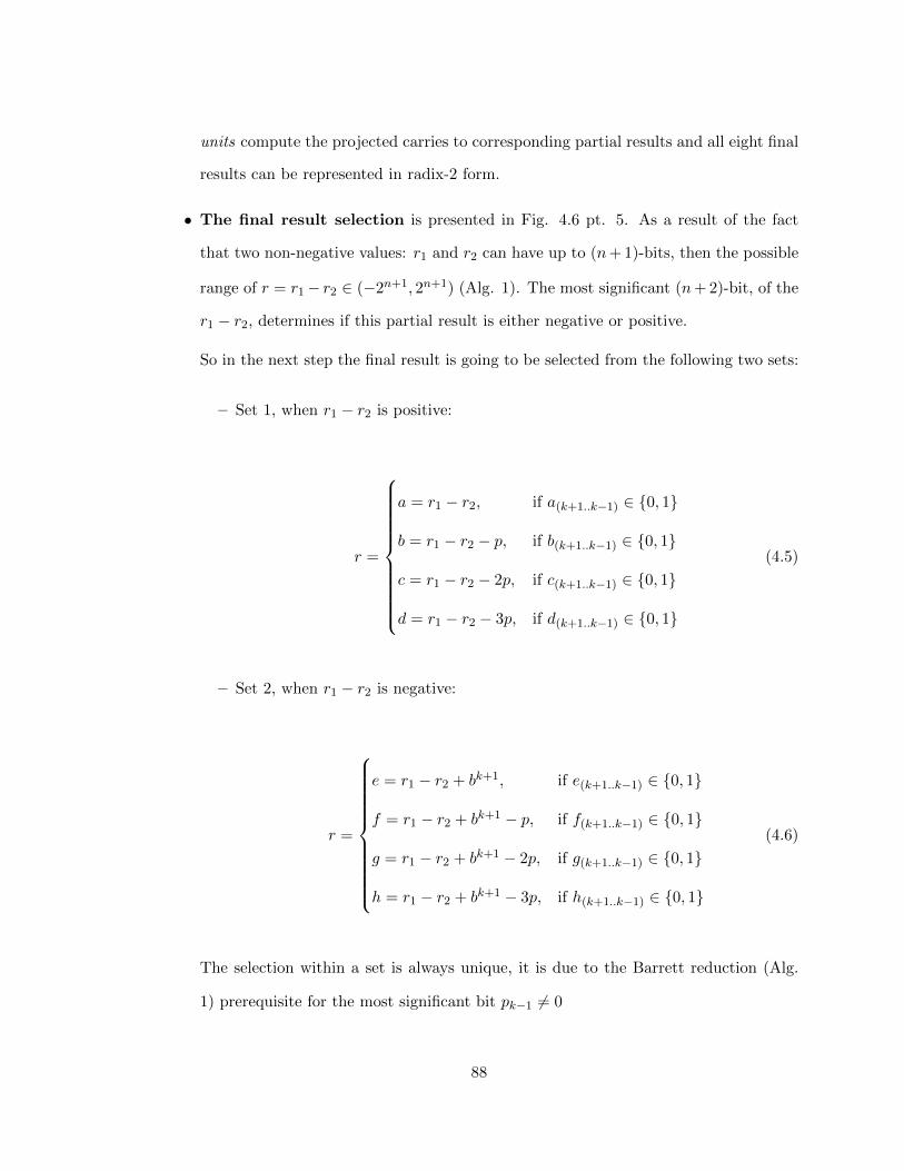
units compute the projected carries to corresponding partial results and all eight final
results can be represented in radix-2 form.
• The final result selection is presented in Fig. 4.6 pt. 5. As a result of the fact
that two non-negative values: r1 and r2 can have up to (n+ 1)-bits, then the possible
range of r = r1− r2 ∈ (−2n+1, 2n+1) (Alg. 1). The most significant (n+ 2)-bit, of the
r1 − r2, determines if this partial result is either negative or positive.
So in the next step the final result is going to be selected from the following two sets:
– Set 1, when r1 − r2 is positive:
r =
a = r1 − r2, if a(k+1..k−1) ∈ {0, 1}
b = r1 − r2 − p, if b(k+1..k−1) ∈ {0, 1}
c = r1 − r2 − 2p, if c(k+1..k−1) ∈ {0, 1}
d = r1 − r2 − 3p, if d(k+1..k−1) ∈ {0, 1}
(4.5)
– Set 2, when r1 − r2 is negative:
r =
e = r1 − r2 + bk+1, if e(k+1..k−1) ∈ {0, 1}
f = r1 − r2 + bk+1 − p, if f(k+1..k−1) ∈ {0, 1}
g = r1 − r2 + bk+1 − 2p, if g(k+1..k−1) ∈ {0, 1}
h = r1 − r2 + bk+1 − 3p, if h(k+1..k−1) ∈ {0, 1}
(4.6)
The selection within a set is always unique, it is due to the Barrett reduction (Alg.
1) prerequisite for the most significant bit pk−1 6= 0
88

4.4 Conclusions
The reduction technique proposed in [119] is not applicable for all Solinas primes, in par-
ticular for those which are used in Pairing-based Cryptography.
First, we have demonstrated that Solinas primes can benefit from the modified Barrett
reduction algorithm and then we have proposed conditions for efficient arithmetic based
on those primes. Next, we have optimized a grid method for multiplication to match the
structure of the digital signal processing blocks (DSP units), embedded in the modern
FPGA devices.
This simple, but very flexible design can give us some unique features - e.g.: it allows us
to speed up single multiplication by using two multipliers. This special feature is especially
attractive in case of n multiplications to be executed using m available multipliers where n
divides m. (e.g.: two multiplications executed using four multipliers, which is the case in
our pairing coprocessor described in Chapter V).
Finally, we have combined both concepts: the grid multiplication method optimized for
FPGAs and the Barrett reduction for Solinas primes, and as a result we have obtained, an
optimal, modular multiplier for pairing-friendly Solinas primes.
89

Chapter 5: Pairing on Edwards curves for
speed-oriented applications
In this chapter are going to demonstrate the fastest to date, a high speed hardware
accelerator for the Tate pairing on twisted supersingular Edwards curves over prime
fields. This coprocessor was built upon the hardware architectures proposed for Solinas
primes and the hybrid high-radix carry save and parallel prefix network adder.
Contents
5.1 Introduction and motivation . . . . . . . . . . . . . . . . . . . . . 90
5.2 Previous work . . . . . . . . . . . . . . . . . . . . . . . . . . . . . 94
5.3 Tate pairing on twisted supersingular Edwards curves . . . . . 95
5.4 The coprocessor . . . . . . . . . . . . . . . . . . . . . . . . . . . . 106
5.5 Hardware implementation results . . . . . . . . . . . . . . . . . . 118
5.6 Conclusions . . . . . . . . . . . . . . . . . . . . . . . . . . . . . . . 123
5.1 Introduction and motivation
In 1985, Koblitz [111] and Miller [110] independently discovered that elliptic curves can be
used to construct public key cryptosystems. Since then, Elliptic Curve Cryptography(ECC)
has been an important object of studies, leading to multiple practical applications [148],
[149], [150] or [151]. Due to the performance and security reasons, different forms and
types of elliptic curves have been proposed: Hessian [152], Koblitz [153], Jacobian [154],
90
Montgomery [155] and doubling and tripling oriented Doche-Icart-Kohel [156]. A new form
of elliptic curves was recently introduced by Edwards [157]. Bernstein and Lange have
demonstrated multiple improvements and applications to cryptography [158], [159], [160]
and [161]. The details and explicit formulae of most important curves are summarized in
[114].
An operation of bilinear pairing on elliptic curve has been introduced originally for
cryptanalysis by Frey and Ruck [162] and Menezes, Okamoto and Vanstone [163]. In 1986
Miller [164] proposed the first algorithm for iteratively computing the Weil and Tate pair-
ings. Nowadays, pairing is primarily used in cryptography for constructive reasons: it is a
basis of security schemes for various applications. The versatility of pairing based cryptog-
raphy has made it an important object of studies. Several of pairing-based schemes, such
as tripartite key exchange protocol [165], identity-based encryption [166], identity-based
signatures [167], and short signatures [168], have been proposed in the last decade. Apart
from the mentioned previously Weil and Tate pairing, other popular pairing types were
discovered, e.g.: Eta [169], Ate [170], R-Ate [171] and Optimal-Ate [172].
5.1.1 Motivation
Compared with other popular public key cryptosystems, like Elliptic Curve Cryptography
or RSA [24], pairing is much more computationally demanding. Therefore, the efficient
hardware and software implementations of cryptographic pairing have also received sig-
nificant attention [173], [174], [175], [176], [177], [178] and [179]. However, the hardware
architectures for Edwards curves-based pairing, introduced for supersingular in [37] and
ordinary forms in [180], have not been reported yet.
The National Security Agency released the Fact Sheet NSA Suite B Cryptography [181].
This document recommends a transition into elliptic curve systems instead of classical public
key technology, such as RSA and DSA [120]. Finally, it provides the recommendation for
the underlying modular arithmetic: the prime fields must be used, instead of binary or
91

ternary fields.
The computation of a pairing can be broken down into curve, group and eventually
modular operations in the underlying fields (Fig. 5.1) Thus, having an efficient modular
multiplier is a major component of a high performance pairing processor. In this work, we
are interested in hardware implementation of pairings over large characteristic fields.
One of the possible optimizations is to take advantage of the embedded resources in
the modern FPGA. Practically all FPGA vendors incorporate in modern FPGAs, apart
from basic reconfigurable logic resources [182], also embedded components, such as large
memory blocks [183], DSP units [184], and Fast Carry Chain Adders [182], [185]. These
hardwired FPGA resources, together with meticulously selected prime numbers such as
Mersenne, Fermat, or Solinas [119] primes can serve as a basis of an efficient hardware
modular architecture.
A well known shortcut for modular multiplication modulo a Mersenne number (2k-1),
performing modular reduction without integer division has been generalized by Solinas
in [119]. A big class of Solinas prime numbers and their efficient arithmetic have been
widely accepted and recommended for ECDSA [120]. The aforementioned technique is not
applicable for all Solinas primes (e.g. Solinas primes from [121] (section 7.2)).
Historically, the software implementations of cryptography have been slower than their
FPGA counterparts. Pairing implementations over prime fields on general purpose pro-
cessors are unique in this respect and they have been demonstrated to be as fast as the
hardware architectures [177]. An efficient protection based on the prime field pairing sys-
tems for cross-platform communication is possible.
5.1.2 Contribution
In this effort we are going to demonstrate several new hardware design techniques for Tate
pairing on Edwards curves over prime fields defined in [37]. Major contributions of this
chapter cover four different layers of pairing computations and they are highlighted here:
92

MultiplicationPoint Addition Point Doubling
2Group Operations
1
Squaring Addition SubtractionMultiplication
Field Operations
Scalar Multiplication
Curve Operations
Cryptographic protocols and schemes
Pairings4
Squaring
3
Bilinear Operations
Extension Field Operations
Figure 5.1: Hierarchy of functions in pairing-based cryptosystems
• This chapter presents an application of our Solinas primes-based, modular arithmetic
architectures for addition and multiplication (Fig. 5.1, pt. 1) to the higher level
application - Pairing-based cryptography [186] on supersingular curves.
• It further explores the parallelism in the explicite formulae of group and bilinear
operations. Eventually, operation scheduling for multi-core environment is provided.
(Fig. 5.1, pt. 2)
• It provides a novel approach to the final exponentiation for given parameters (Fig.
5.1, pt. 3).
• It provides first hardware architecture for 80, 120 and 128-bit pairing on Edwards
curves (Fig. 5.1, pt. 4).
• Finally, the proposed design computes 80, 120 and 128-bit secure pairing over prime
field in less than 0.14, 0.54 and 0.70 ms, respectively. It is the fastest pairing imple-
mentation over prime fields in 120-128-bit security range.
The rest of this chapter is organized as follows:
In Section 5.2 we discuss previous work. Section 5.3 is devoted to the Tate pairing on
Edwards curves over prime fields. Section 5.4 describes the proposed coprocessor. Section
5.5 discusses and analyzes the results, finally we draw conclusions in Section 5.6.
93

5.2 Previous work
Baretto and Naehrig have demonstrated a pairing-friendly class of curves for prime fields in
[187] (Barreto-Naehrig (BN) curves). Currently, they are considered the most suitable for
128-bits security level pairing over prime fields. Several coprocessors for the computation
of pairing over aforementioned curves on 128-bit security level were demonstrated in the
literature.
A pairing coprocessor, implemented in Xilinx Virtex-4, demonstrated by Ghosh et al.
in [188], consumes 52 kSlices and it computes the Tate, Ate, and R-ate pairings in 34.6 ms,
24.2 ms, and 16.4 ms, respectively. A design-space exploration of an application-specific
instruction-set processor (ASIP) for the computation of various cryptographic pairings over
BN-curves was investigated by Kammler et al. in [189]. The Montgomery reduction in
a polynomial ring, combined with a coefficient reduction phase, using a pseudo-Mersenne
numbers, helped Fan et al. in [174] to speed-up pairing computation significantly and beat
all previously reported hardware implementations by a factor of 5.
Finally, Cheung et al. in [178] have shown that by combining RNS and lazy reduction,
the speed of pairing computation in hardware can be largely increased. The fastest version
of the proposed coprocessor computes an optimal-Ate pairing at 126-bit security level in
0.573 ms.
This work concentrates on the pairing architectures for prime fields. However, it is
important to underline the fact that traditionally the binary fields-based architectures are
more successful in terms of hardware implementations. The fastest to date FPGA imple-
mentation of the 128-bit secure pairing architecture on supersingular curves over binary
fields was demonstrated in [179].
The Tate pairing on supersingular and ordinary Edwards curves over prime field was
introduced in [37] and [180], respectively.
94
5.3 Tate pairing on twisted supersingular Edwards curves
5.3.1 Twisted Edwards curves
Edwards in [157] has introduced the addition law for the curves x2 + y2 = c2 · (1 + x2 · y2)
over a non-binary field K. Later on, Bernstein and Lange have demonstrated more general
version of Edwards curves defined by x2 + y2 = c2 · (1 + d · x2 · y2), where c, d ∈ K with
c · d·(1 - d · c4) 6= 0. In [158], this form was generalized to twisted Edwards form defined by
Ea,d : a · x2 + y2 = 1 + d · x2 · y2, (5.1)
where a, d ∈ K with a ·d · (a−d) 6= 0. Edwards curves became then a special case of twisted
Edwards curves, where a is equal to 1.
A supersingular form of Edwards curves has been investigated by Das and Sarkar in
[37]. They have presented the application of the supersingular twisted Edwards curves for
the pairing computations in the aforementioned paper.
5.3.2 Tate pairing on supersingular Edwards curves
In general, pairing transformation e (Eq. 5.2) takes two arguments (two elliptic curve points
P and Q from two algebraic groups G1 and G2) and produce an element F of the third
algebraic group GT .
F ← e(P,Q), (5.2)
where P ∈ G1, Q ∈ G2, F ∈ GT .
The most important properties of these transformations are: bilinearity (∀a, b ∈ Zp :
e(a·P, b·Q) = e(P,Q)a·b), non-degeneracy (function e(P ,Q) never returns ’1’), and efficiency
95
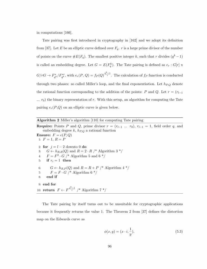
in computations [166].
Tate pairing was first introduced in cryptography in [162] and we adopt its definition
from [37]. Let E be an elliptic curve defined over Fq. r is a large prime divisor of the number
of points on the curve #E(Fq). The smallest positive integer k, such that r divides (qk− 1)
is called an embedding degree. Let G = E(F kq ). The Tate pairing is defined as er : G[r] x
G/rG→ F ∗qk/F ∗r
qk, with er(P , Q) = fP (Q)
qk−1r . The calculation of fP function is conducted
through two phases: so called Miller’s loop, and the final exponentiation. Let hP,Q denote
the rational function corresponding to the addition of the points: P and Q. Let r = (rl−1
... r0) the binary representation of r. With this setup, an algorithm for computing the Tate
pairing er(P ,Q) on an elliptic curve is given below.
Algorithm 2 Miller’s algorithm [110] for computing Tate pairing
Require: Points P and Q, prime divisor r = (rl−1 ... r0), rl−1 = 1, field order q, andembedding degree k, hP,Q a rational function
Ensure: F = e(P,Q)1: F = 1, R = P
2: for j = l − 2 downto 0 do3: G← hR,R(Q) and R = 2 ·R /* Algorithm 3 */
4: F = F 2 ·G /* Algorithm 5 and 6 */5: if ri = 1 then
6: G← hR,P (Q) and R = R+ P /* Algorithm 4 */
7: F = F ·G /* Algorithm 6 */8: end if
9: end for
10: return F ← Fqk−1
r /* Algorithm 7 */
The Tate pairing by itself turns out to be unsuitable for cryptographic applications
because it frequently returns the value 1. The Theorem 2 from [37] defines the distortion
map on the Edwards curve as
φ(x, y) = (x · i, 1
y), (5.3)
96

where i is the imaginary unit, such that i2 = −1. This additional mapping prevents the
Tate pairing from returning 1. The explicit formulae for particular Tate pairing parts are
discussed below.
Algorithm 3 Doubling and computation of Miller value using projective Edwards coordi-nates
Require: R = (xR, yR, zR), precomputed values: c1(Eq.5.4), c2(Eq.5.5), c3(Eq.5.6)Ensure: 2R = (x2R, y2R, z2R), G = g1 · i+ g2)
1: b← (xR + yR)2
2: c← x2R
3: d← y2R
4: e← c+ d5: h← z2
R6: j ← e− 2 · h7: be← b− e8: x2R ← be · j9: k ← c− d
10: y2R ← e · k11: z2R ← e · j12: l← (yR + zR)2
13: m← l − d− h14: n← 2 · h15: cc← be · (n−m)16: dd← n · (2 · e− n−m)17: ee← m · (m− 2 · c)18: g1 ← c1 · cc19: g2 ← c2 · (dd− ee) + c3 · ee− dd20: return 2R = (x2R, y2R, z2R), G = g1 · i+ g2
5.3.3 Miller loop
Let E be an elliptic curve and the points: P and Q ∈ E(Fq) are the arguments for the
Tate pairing (Alg. 2). First, argument P = (XP , YP ) is given using so called projective
coordinates (xP , yP , zP ), where XP = xPzP
and YP = yPzP
. The second argument, point Q
is given in affine coordinates as (xQ, yQ), but it can be used after the distortion map (Eq.
5.3) was applied: φ(Q) = (xQ · i, 1yQ
).
In order to compute a pairing value for P and Q, Das and Sarkar proposed to use the
dedicated addition (Alg. 4) and doubling (Alg. 3) formulae.
97

Algorithm 4 Addition and computation of Miller value using projective Edwards coordi-nates
Require: P = (xP , yP , zP ), R = (xR, yR, zR), precomputed values:c1(Eq.5.4), c2(Eq.5.5), c3(Eq.5.6), curve parameter - dE
Ensure: R = P +R = (xP+R, yP+R, zP+R), G = g1 · i+ g2
1: a← (zP · zR)
2: b← a2
3: c← xP · xR4: d← yP · yR5: e← dE · c · d6: f ← b− e7: g ← b+ e8: h← (xP + yP ) · (xR + yR)− c− d9: m← a · (d− c)
10: xP+R ← a · f · h11: yP+R ← g ·m12: zP+R ← f · g13: j ← (zP − yP ) · (zR + yR)− a+ d14: k ← (xP − zP ) · (xR + zR)− c+ a15: cc← c · j16: dd← a · (2 · xR · yP − h− k)17: ee← −xR · zP · j + (d+ yP · zR) · k18: g1 ← c1 · cc19: g2 ← c2 · (dd− ee) + c3 · ee− dd20: return P +R = (xP+R, yP+R, zP+R), G = g1 · i+ g2
98
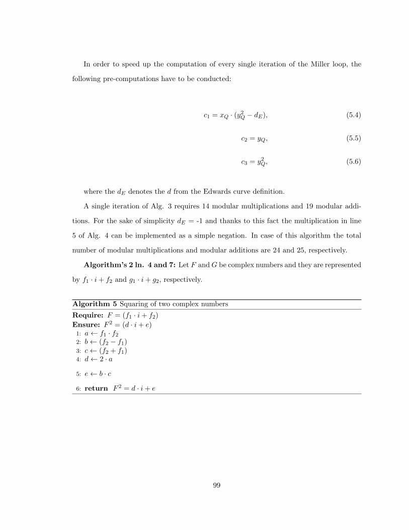
In order to speed up the computation of every single iteration of the Miller loop, the
following pre-computations have to be conducted:
c1 = xQ · (y2Q − dE), (5.4)
c2 = yQ, (5.5)
c3 = y2Q, (5.6)
where the dE denotes the d from the Edwards curve definition.
A single iteration of Alg. 3 requires 14 modular multiplications and 19 modular addi-
tions. For the sake of simplicity dE = -1 and thanks to this fact the multiplication in line
5 of Alg. 4 can be implemented as a simple negation. In case of this algorithm the total
number of modular multiplications and modular additions are 24 and 25, respectively.
Algorithm’s 2 ln. 4 and 7: Let F andG be complex numbers and they are represented
by f1 · i+ f2 and g1 · i+ g2, respectively.
Algorithm 5 Squaring of two complex numbers
Require: F = (f1 · i+ f2)
Ensure: F 2 = (d · i+ e)1: a← f1 · f2
2: b← (f2 − f1)3: c← (f2 + f1)4: d← 2 · a
5: e← b · c
6: return F 2 = d · i+ e
99

Table 5.1: Parameters of Solinas primes used for Tate pairing on supersingular twistedEdwards curves
Security Field order - q Prime divisor - r Exponent - e = qk−1r
80-bits 2520 + 2363 − 2360 − 1 2160 + 23 − 1 2880 + 2723 − 2721 + 2720 − 2361
120-bits 21263 +21037−21005−1 2258 + 232 − 1 22268 +22042−22011 +22010−21006
128-bits 21492 +21237−21224−1 2268 + 213 − 1 22716 +22461−22449 +22448−21225
191-bits 23955 +23581 +23573−1 2382 + 28 − 1 27528 +27154−27147 +27146−23574
Algorithm 6 Multiplication of two complex numbers
Require: F = (f1 · i+ f2) and G = (g1 · i+ g2)Ensure: F ·G = (e · i+ g)1: a← f1 · g2
2: b← f2 · g1
3: c← f2 · g2
4: d← f1 · g1
5: e← a+ b
6: g ← c+ d
7: return F ·G = e · i+ g
Then, the computation of Alg. 2 ln. 4 requires an execution of Alg. 5 (F 2), and then
execution of Alg. 6 (F · G). In case of Alg. 2 ln. 7, an execution of Alg. 6 (F · G) is
sufficient. Finally, the ln. 4 demands 6 modular multiplications and 5 modular additions.
For ln. 7 these numbers are 4 and 2, respectively.
Due to the fact that the modular addition operation is relatively cheap, in terms of
circuitry and calculation’s latency, then the number of modular multiplication indicates
the complexity of every operation. In case of 80-bit, 120-bit and 128-bit security level the
number of modular multiplications are 5036, 10584 and 11148 respectively.
100

5.3.4 Choice of parameters for supersingular curves with embedding de-
gree k=2
The security of pairing-based cryptography for different type of curves is discussed in [121].
Choice of parameters and the generation procedure for supersingular curves with embed-
ding degree k=2 was presented in section 7.2 of this paper. Koblitz and Menezes have
recommended prime numbers of the form 2a1 ± 2a2 ± 1, so called Solinas primes [119], to be
used for a prime divisor r and a prime field order q.
The Pollard’s rho method is the fastest known algorithm for solving the ECDLP [190].
For an implementation details of this method we recommend [191].
Function field sieve algorithm is the fastest known method for solving the DLP in the
extension field. Detailed discussion about the time complexity of this method was conducted
by Joux at el. in [192]. They have summarized that the FFS complexity is usually expressed
using the following function:
Lq(α, c) = exp((c+ o(1))(log(q))α(log(log(q)))1−α, (5.7)
where log denotes natural logarithm. In particular, for the prime field Fp and for binary
fields F2n , the number field sieve and the function field sieve respectively yield Lp(13 , (64
9 )13 )
and L2n(13 , (32
9 )13 ) algorithms.
Later on, Schirokauer in [193] has defined the weight of integer to be the smallest w such
that the integer p can be represented as∑w
i=1 ξi2ai , with ξ1, ..., ξw ∈ {−1, 1} and ai ∈ Zp.
He has conducted an analysis of the number field sieve time complexity for integers of low
weight. He has demonstrated that a prime field of the order q with weight w yield Lp(13 ,
(32τ2
9 )13 ), where τ2 is converging to 2w−3
w−1 . The Solinas primes, considered in this work, have
their weight w = 4.
101

In order to generate parameters for different security levels we took into account re-
sistance against aforementioned cryptanalytical methods. Among all the generated pairs:
prime divisor r and prime field p, we have selected those with the lowest hamming weight
of Barrett’s µ parameter (Eq. 4.4). This assumption allows the most efficient computation
of the multiplication by the constant µ number from the Alg. 1.
Table 5.1 summarizes the sizes of field, prime divisor, and the exponent value - the most
important parameters in case of pairing based on supersingular curves.
5.3.5 Final exponentiation
In regards to the computations of the line 10 of Alg. 2 (F ← Fqk−1
r ), so called, the final ex-
ponentiation, Koblitz and Menezes show in [121] that this computation can be significantly
simplified. In case of supersingular curves with embedding degree k = 2, the expression
q2−1r can be split into two terms: (q − 1) · q+1
r (from the definition of supersingularity of
elliptic curves we know that r always divides q + 1). Calculating F′ ← F q−1 can be easily
obtained though a cheap Frobenius computations and an inversion. The second step is to
calculate F′ q+1
r which is so called, the hard part of the final exponentiation. Due to the
fact that the computational cost of inversion (Eq. 5.10) is similar to calculating F q−1, this
method is not as effective for embedding degree k = 2.
However the final exponentiation, with an exponent in a Solinas form, can be sped up
significantly using a simple trick summarized below.
Let F be a complex number and e = 2a1 +2a2−2a3 +2a4−2a5 , where a1, a2, a3, a4, a5 are
integers and a1 > a2 > a3 > a4 > a5. In particular, a set of (a1, a2, a3, a4, a5) corresponds
to the (880, 723, 721, 720, 361), a set of powers representing the fixed-exponent e for 80-bit
security level (Table 5.1). In order to perform a fixed-exponent exponentiation of a complex
number:
102
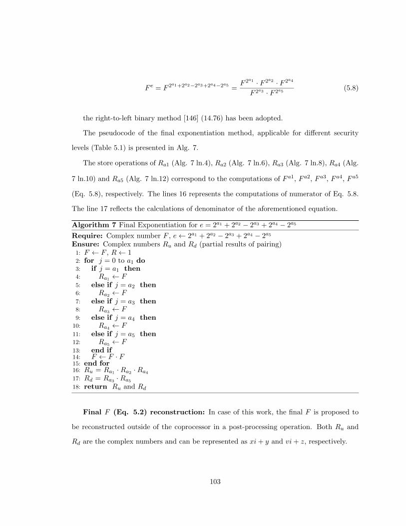
F e = F 2a1+2a2−2a3+2a4−2a5 =F 2a1 · F 2a2 · F 2a4
F 2a3 · F 2a5(5.8)
the right-to-left binary method [146] (14.76) has been adopted.
The pseudocode of the final exponentiation method, applicable for different security
levels (Table 5.1) is presented in Alg. 7.
The store operations of Ra1 (Alg. 7 ln.4), Ra2 (Alg. 7 ln.6), Ra3 (Alg. 7 ln.8), Ra4 (Alg.
7 ln.10) and Ra5 (Alg. 7 ln.12) correspond to the computations of F a1, F a2, F a3, F a4, F a5
(Eq. 5.8), respectively. The lines 16 represents the computations of numerator of Eq. 5.8.
The line 17 reflects the calculations of denominator of the aforementioned equation.
Algorithm 7 Final Exponentiation for e = 2a1 + 2a2 − 2a3 + 2a4 − 2a5
Require: Complex number F , e← 2a1 + 2a2 − 2a3 + 2a4 − 2a5
Ensure: Complex numbers Ru and Rd (partial results of pairing)1: F ← F , R← 12: for j = 0 to a1 do3: if j = a1 then4: Ra1 ← F5: else if j = a2 then6: Ra2 ← F7: else if j = a3 then8: Ra3 ← F9: else if j = a4 then
10: Ra4 ← F11: else if j = a5 then12: Ra5 ← F13: end if14: F ← F · F15: end for16: Ru = Ra1 ·Ra2 ·Ra417: Rd = Ra3 ·Ra518: return Ru and Rd
Final F (Eq. 5.2) reconstruction: In case of this work, the final F is proposed to
be reconstructed outside of the coprocessor in a post-processing operation. Both Ru and
Rd are the complex numbers and can be represented as xi+ y and vi+ z, respectively.
103

F ← RuRd← x · i+ y
v · i+ z(5.9)
The formulae of complex numbers modular inversion are demonstrated in Eq. 5.10.
(v · i+ z)−1 = (v′ · i+ z′) =
v′ = −v
z2+v2
z′ = zz2+v2
(5.10)
The final F of the Tate pairing on twisted supersingular Edwards curves over prime
fields is a product of (x · i+ y) and (v′ · i+ z′).
Hardware coprocessor-related decisions and comments:
The analysis of explicit formulae of algorithms presented above and the parameters
choice helped us to draw some conclusions about hardware architecture for Edwards curves-
based pairing coprocessor:
• Due to the dependencies between the intermediate values of computations in Alg.
3, Alg. 4 and Alg. 7, the implementation of all the multiplications independently
would be inefficient (Most of the circuit would be inactive during most of the pairing
computations).
• The number of modular multiplications in lines 3-4 in Alg. 2, and lines 7-8 in Alg. 2 are
20 and 28, respectively. An analysis of internal data dependencies in aforementioned
algorithms revealed that it is relatively easy to separate up to four, equally balanced
streams of data. At this point two possible scenarios were possible: either hardware
architecture based on modular multiplier with four pipelining stages or with four
independent modular multiplication units.
• An analysis of the data dependency between consecutive iterations of Alg. 7, led us
to the conclusion that pipelining-oriented solution will lead to longer computational
104

time than the alternative solution. Moreover, one more crucial requirement for the
multiplier arose - an ability to reduce by factor of 2 (using the double speed mode
described in the next section) the multiplication time in case of the availability of
twice as many resources compared to the basic mode.
• The most successful modular multipliers, reported in the literature, were based on
DSP units (Sec. 4.2). However, the RNS-based unit from [178] utilizes multi-stages
pipelining, and therefore the scheduling of Alg. 7 (only results of two multiplications
per iteration have to be computed) would always lead to huge number of idle states.
Tripartite module [127] requires enormous number of DSP blocks for the operand sizes
from Table 5.1 and the design from [134] is highly optimized for RSA algorithm - it was
design for a computations where one of the arguments is not changing and it has not
been optimized for interleaving with other operations (like addition or subtraction).
A hardware multiplier for Tate pairing on twisted supersingular Edwards curves was
inspired by aforementioned designs and it was presented in the previous chapter.
105

5.4 The coprocessor
In this section, we propose an application, for the previously described modular architectures
for Solinas primes, a latency-optimized coprocessor for Tate pairing on Edwards curves.
First, a high-level description of the hardware accelerator will be provided. Then we
are going to discuss operation scheduling for the four different operational modes of this
circuit: doubling and addition operations in the Miller loop, complex numbers squaring in
the Final exponentiation and eventually, the calculation of Ru and Rd (Eq. 5.9).
Top level block diagram of the coprocessor datapath: is demonstrated in Fig.
5.2. Two major group of components in this accelerator are: a bank of memories (memory
map in Table 5.2) for the intermediate results of a pairing computations, and the arithmetic
modules. In order to enable the basic operations to work on entire length of the arguments
the memories were organized in parallel (Fig. 5.2 Pt. 2). Therefore, an argument R
= {r(n − 1), ... r(0)} can be stored/fetched in a single clock cycle. To start a pairing
computation these memories have to be initialized properly. Precomputed constants c1
(Eq. 5.4), c2 (Eq. 5.5) and c3 (Eq. 5.6), coordinates of the point P , initial value of the F
have to be introduced from the external environment through the input bus (Fig. 5.2 Pt.
1) and stored in the bank of memories (Fig. 5.2 Pt. 2). The computational resources of
our coprocessor consist of four multipliers (Fig. 5.2 Pt. 3), single fully pipelined modular
reductor (Fig. 5.2 Pt. 5) and a pipelining modular adder (Fig. 5.2 Pt. 6).
Table 5.4: Scheduling of operations for Alg. 2, when ri = 1
Multiplier 1 Multiplier 2 Multiplier 3 Multiplier 4 Adder
Continued on next page
106
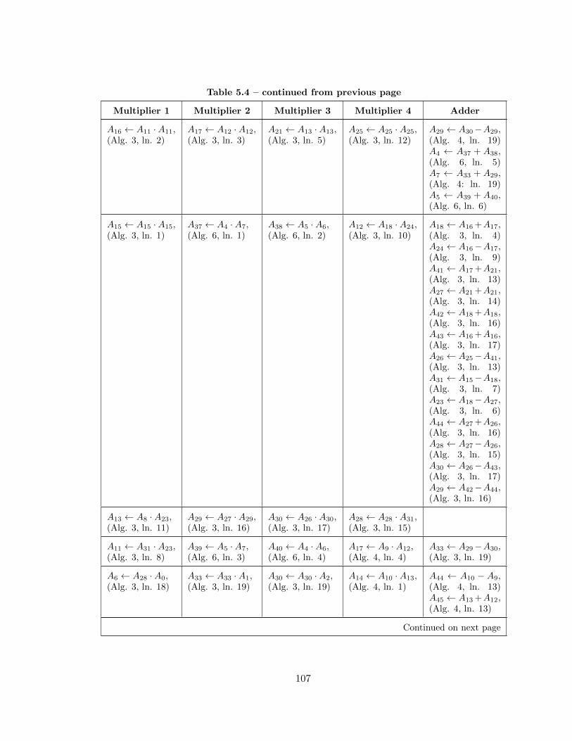
Table 5.4 – continued from previous page
Multiplier 1 Multiplier 2 Multiplier 3 Multiplier 4 Adder
A16 ← A11 ·A11,(Alg. 3, ln. 2)
A17 ← A12 ·A12,(Alg. 3, ln. 3)
A21 ← A13 ·A13,(Alg. 3, ln. 5)
A25 ← A25 ·A25,(Alg. 3, ln. 12)
A29 ← A30−A29,(Alg. 4, ln. 19)A4 ← A37 + A38,(Alg. 6, ln. 5)A7 ← A33 + A29,(Alg. 4: ln. 19)A5 ← A39 + A40,(Alg. 6, ln. 6)
A15 ← A15 ·A15,(Alg. 3, ln. 1)
A37 ← A4 ·A7,(Alg. 6, ln. 1)
A38 ← A5 ·A6,(Alg. 6, ln. 2)
A12 ← A18 ·A24,(Alg. 3, ln. 10)
A18 ← A16 +A17,(Alg. 3, ln. 4)A24 ← A16−A17,(Alg. 3, ln. 9)A41 ← A17 +A21,(Alg. 3, ln. 13)A27 ← A21 +A21,(Alg. 3, ln. 14)A42 ← A18 +A18,(Alg. 3, ln. 16)A43 ← A16 +A16,(Alg. 3, ln. 17)A26 ← A25−A41,(Alg. 3, ln. 13)A31 ← A15−A18,(Alg. 3, ln. 7)A23 ← A18−A27,(Alg. 3, ln. 6)A44 ← A27 +A26,(Alg. 3, ln. 16)A28 ← A27−A26,(Alg. 3, ln. 15)A30 ← A26−A43,(Alg. 3, ln. 17)A29 ← A42−A44,(Alg. 3, ln. 16)
A13 ← A8 ·A23,(Alg. 3, ln. 11)
A29 ← A27 ·A29,(Alg. 3, ln. 16)
A30 ← A26 ·A30,(Alg. 3, ln. 17)
A28 ← A28 ·A31,(Alg. 3, ln. 15)
A11 ← A31 ·A23,(Alg. 3, ln. 8)
A39 ← A5 ·A7,(Alg. 6, ln. 3)
A40 ← A4 ·A6,(Alg. 6, ln. 4)
A17 ← A9 ·A12,(Alg. 4, ln. 4)
A33 ← A29−A30,(Alg. 3, ln. 19)
A6 ← A28 ·A0,(Alg. 3, ln. 18)
A33 ← A33 ·A1,(Alg. 3, ln. 19)
A30 ← A30 ·A2,(Alg. 3, ln. 19)
A14 ← A10 ·A13,(Alg. 4, ln. 1)
A44 ← A10 − A9,(Alg. 4, ln. 13)A45 ← A13 +A12,(Alg. 4, ln. 13)
Continued on next page
107

Table 5.4 – continued from previous page
Multiplier 1 Multiplier 2 Multiplier 3 Multiplier 4 Adder
A29 ← A11 ·A9,(Alg. 4, ln. 16)
A16 ← A8 ·A11,(Alg. 4, ln. 3)
A23 ← A44 ·A45,(Alg. 4, ln. 13)
A18 ← A3 ·A17,(Alg. 4, ln. 5)
A4 ← A37 + A38,(Alg. 6, ln. 5)A5 ← A39 + A40,(Alg. 6, ln. 6)A34 ← A5 − A4,(Alg. 5, ln. 2)A35 ← A5 + A4,(Alg. 5, ln. 3)A44 ← A10 + A9,(Alg. 4, ln. 8)A45 ← A11 +A12,(Alg. 4, ln. 8)
A36 ← A4 ·A5,(Alg. 5, ln. 1)
A5 ← A34 ·A35,(Alg. 5, ln. 5)
A21 ← A44 ·A45,(Alg. 4, ln. 8)
A15 ← A14 ·A14,(Alg. 4, ln. 2)
A29 ← A30−A29,(Alg. 3, ln. 19)A49 ← A17−A14,(Alg. 4, ln. 13)A50 ← A8 − A10,(Alg. 4, ln. 14)A51 ← A11 +A13,(Alg. 4, ln. 14)A43 ← A16 +A17,(Alg. 4, ln. 8)A22 ← A17−A16,(Alg. 4, ln. 9)A7 ← A33 + A29,(Alg. 3, ln. 19)
A52 ← A11 ·A10,(Alg. 4, ln. 17)
A53 ← A9 ·A13,(Alg. 4, ln. 17)
A24 ← A50 ·A51,(Alg. 4, ln. 14)
A26 ← A14 ·A22,(Alg. 4, ln. 9)
A4 ← A36 + A36,(Alg. 5, ln. 4)A29 ← A29 +A29,(Alg. 4, ln. 16)A23 ← A23 +A49,(Alg. 4, ln. 13)A29 ← A29−A21,(Alg. 4, ln. 16)A47 ← A14−A16,(Alg. 4, ln. 14)
A11 ← A21 ·A14,(Alg. 4, ln. 10)
A18 ← A18 ·A16,(Alg. 4, ln. 5)
A37 ← A4 ·A7,(Alg. 6, ln. 1)
A38 ← A5 ·A6,(Alg. 6, ln. 2)
A53 ← A53 +A17,(Alg. 4, ln. 17)A21 ← A21−A43,(Alg. 4, ln. 8)A24 ← A24 +A47,(Alg. 4, ln. 14)A29 ← A29−A24,(Alg. 4, ln. 16)
Continued on next page
108

Table 5.4 – continued from previous page
Multiplier 1 Multiplier 2 Multiplier 3 Multiplier 4 Adder
A28 ← A16 ·A23,(Alg. 4, ln. 15)
A29 ← A14 ·A29,(Alg. 4, ln. 16)
A52 ← A52 ·A23,(Alg. 4, ln. 17)
A53 ← A53 ·A24,(Alg. 4, ln. 17)
A19 ← A15−A18,(Alg. 4, ln. 6)A20 ← A15 +A18,(Alg. 4, ln. 7)
A11 ← A11 ·A19,(Alg. 4, ln. 10)
A13 ← A19 ·A20,(Alg. 4, ln. 12)
A12 ← A20 ·A22,(Alg. 4, ln. 11)
A39 ← A5 ·A7,(Alg. 6, ln. 3)
A30 ← A53−A52,(Alg. 4, ln. 17)A33 ← A30−A29,(Alg. 4, ln. 19)
A4 ← A28 ·A0,(Alg. 4, ln. 18)
A33 ← A33 ·A1,(Alg. 4, ln. 19)
A30 ← A30 ·A2,(Alg. 4, ln. 19)
A40 ← A4 ·A6,(Alg. 6, ln. 4)
A15 ← A11 +A12,(Alg. 3, ln. 1)A25 ← A12 +A13,(Alg. 3, ln. 12)
Due to the fact that the multiplication circuit works in a sequential fashion, the only
possible way to improve the total latency of several, independent (the result of one mul-
tiplication is not an argument to the next multiplication), consecutive multiplication is to
instantiate multiple such units. In case of tate pairing on super singular Edwards curves
the numbers of multiplications per iteration in following cases: Alg. 2 (line 3 and 4), Alg.
2 (line 5 and 6), Alg. 7 (line 14) and Alg. 7 (lines 16-17) are 20, 48, 2, 12, respectively.
The greatest common factor of all those numbers is two, and this could be a first choice for
the number of multiplication units.
In order to further improve the latency of the pairing computations we have decide to
instantiate four such units. This allow us to conduct the computations of a single iteration
of Alg. 2 (line 3 and 4), Alg. 2 (line 5 and 6), and and Alg. 7 (lines 16-17) in five, twelve
and three phases.
The two multiplication of the single iteration of the final exponentiation doubling opera-
tion (Alg. 7 (line 14)) can be computed within one phase. All four multiplication units, used
in the double speed mode, are employed for the computations of partial products of afore-
mentioned two multiplications. The final products of them are computed using additional
circuit (Fig. 5.2 Pt. 4).
109

r(N−1)1
2
3
for the double speed modeAdditional circuit
System Multipliexer
Modular Reductor
4
5
6
78
R
17N
........
in17
17
DPRAM
17
17 17a(0) b(0)
A B
a(0)
DPRAM
#0
r(0)
out
A
17
PISO
b(0)
Multiplier #1
A B
Multiplier #2 #3
A B A B A B A B
ModularAdder
#4Multiplier Multiplier
Number of 17−bit words:
N = 31 (80−bit), 75 (120−bit), 88 (128−bit)
A = {a(N−1), ... a(0)}, B = {b(N−1), ...b(0)}, R = {r(N−1), ... r(0)}
17N
17N
34N
17N 17N
17N
b(N−1)a(N−1)
#N−1
b(N−1)a(N−1)
Figure 5.2: Top level block diagram of pairing coprocessor
110
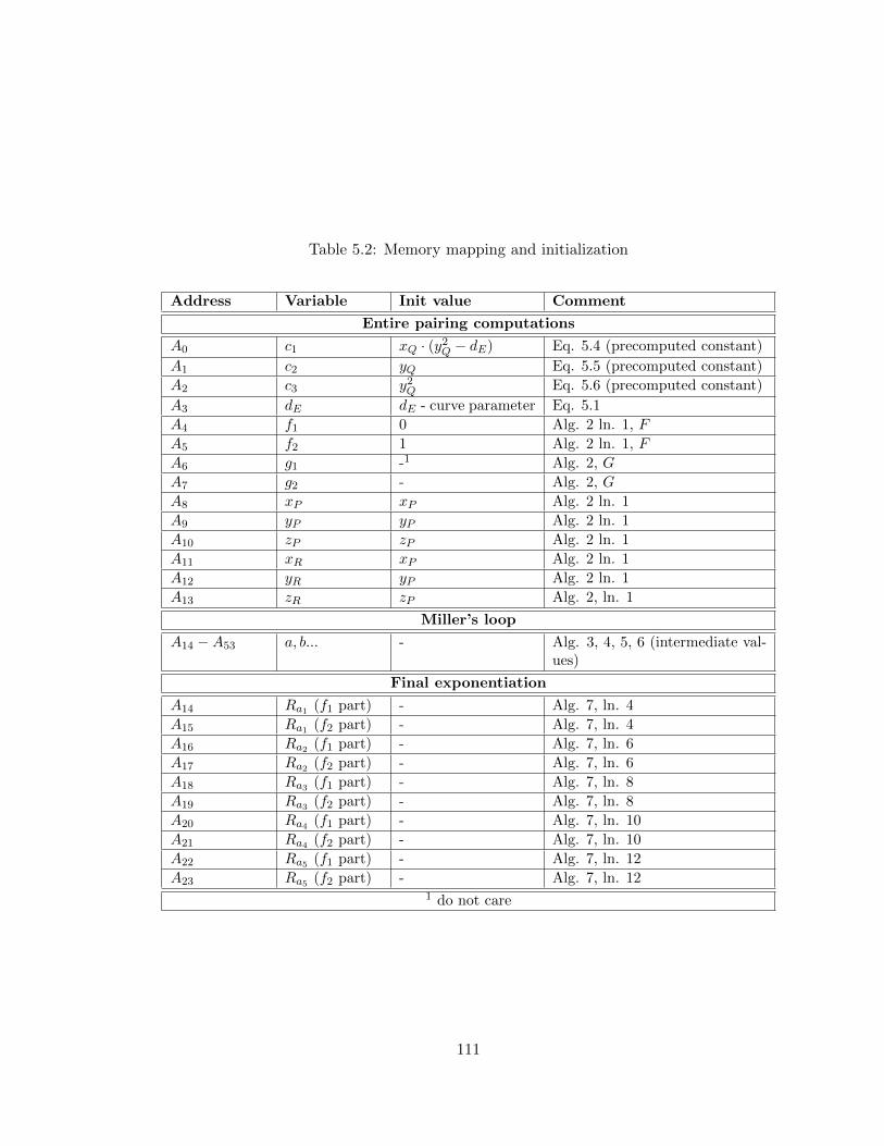
Table 5.2: Memory mapping and initialization
Address Variable Init value Comment
Entire pairing computations
A0 c1 xQ · (y2Q − dE) Eq. 5.4 (precomputed constant)
A1 c2 yQ Eq. 5.5 (precomputed constant)
A2 c3 y2Q Eq. 5.6 (precomputed constant)
A3 dE dE - curve parameter Eq. 5.1
A4 f1 0 Alg. 2 ln. 1, F
A5 f2 1 Alg. 2 ln. 1, F
A6 g1 -1 Alg. 2, G
A7 g2 - Alg. 2, G
A8 xP xP Alg. 2 ln. 1
A9 yP yP Alg. 2 ln. 1
A10 zP zP Alg. 2 ln. 1
A11 xR xP Alg. 2 ln. 1
A12 yR yP Alg. 2 ln. 1
A13 zR zP Alg. 2, ln. 1
Miller’s loop
A14 −A53 a, b... - Alg. 3, 4, 5, 6 (intermediate val-ues)
Final exponentiation
A14 Ra1 (f1 part) - Alg. 7, ln. 4
A15 Ra1 (f2 part) - Alg. 7, ln. 4
A16 Ra2 (f1 part) - Alg. 7, ln. 6
A17 Ra2 (f2 part) - Alg. 7, ln. 6
A18 Ra3 (f1 part) - Alg. 7, ln. 8
A19 Ra3 (f2 part) - Alg. 7, ln. 8
A20 Ra4 (f1 part) - Alg. 7, ln. 10
A21 Ra4 (f2 part) - Alg. 7, ln. 10
A22 Ra5 (f1 part) - Alg. 7, ln. 12
A23 Ra5 (f2 part) - Alg. 7, ln. 121 do not care
111

Table 5.3: Scheduling of operations for Alg. 2, when ri = 0
Multiplier 1 Multiplier 2 Multiplier 3 Multiplier 4 Adder
A16 ← A11 ·A11,(Alg. 3, ln. 2)
A17 ← A12 ·A12,(Alg. 3, ln. 3)
A21 ← A13 ·A13,(Alg. 3, ln. 5)
A25 ← A25 ·A25,(Alg. 3, ln. 12)
A29 ← A30 − A29, (Alg. 3,ln. 19) A4 ← A37 + A38,(Alg. 6, ln. 5) A7 ← A33 +A29, (Alg. 3: ln. 19) A5 ←A39 + A40, (Alg. 6, ln. 6)A34 ← A5 −A4, (Alg. 5, ln.2) A35 ← A5 + A4, (Alg. 5,ln. 3)
A15 ← A15 ·A15,(Alg. 3, ln. 1)
A36 ← A4 ·A5,(Alg. 5, ln. 1)
A5 ← A34 ·A35,(Alg. 5, ln. 5)
A12 ← A18 ·A23,(Alg. 3, ln. 10)
A18 ← A16 + A17, (Alg. 3,ln. 4) A24 ← A16 − A17,(Alg. 3, ln. 9) A41 ←A17 + A21, (Alg. 3, ln. 13)A27 ← A21 + A21, (Alg. 3,ln. 14) A42 ← A18 + A18,(Alg. 3, ln. 16) A43 ←A16 + A16, (Alg. 3, ln. 17)A26 ← A25 + A41, (Alg. 3,ln. 13) A31 ← A15 − A18,(Alg. 3, ln. 7) A23 ←A18 − A27, (Alg. 3, ln. 6)A44 ← A27 + A26, (Alg. 3,ln. 16) A28 ← A27 − A26,(Alg. 3, ln. 15) A30 ←A26 − A43, (Alg. 3, ln. 17)A29 ← A42 − A44, (Alg. 3,ln. 16)
A13 ← A18 ·A24,(Alg. 3, ln. 11)
A29 ← A27 ·A29,(Alg. 3, ln. 16)
A30 ← A26 ·A30,(Alg. 3, ln. 17)
A28 ← A28 ·A31,(Alg. 3, ln. 15)
A4 ← A36 +A36, (Alg. 5, ln.4)
A11 ← A32 ·A24,(Alg. 3, ln. 8)
A37 ← A4 ·A7,(Alg. 6, ln. 1)
NegueshaA38 ← A5 ·A6,(Alg. 6, ln. 2)
A39 ← A5 ·A7,(Alg. 6, ln. 3)
A25 ← A12 + A13, (Alg. 3,ln. 12) A15 ← A11 + A12,(Alg. 3, ln. 1) A33 ← A29 −A30, (Alg. 3, ln. 19)
A40 ← A4 ·A6,(Alg. 6, ln. 4)
A6 ← A0 ·A28,(Alg. 3, ln. 18)
A33 ← A1 ·A33,(Alg. 3, ln. 19)
A30 ← A2 ·A30,(Alg. 3, ln. 19)
112

Table 5.5: Final exponentiation Alg. 7 scheduling.MSP(x) and LSP(x) - the most and the least significant parts of x-value, respectively.
Multiplier 1 Multiplier 2 Multiplier 3 Multiplier 4 Adder
Alg. 7 ln. 14 is computed using Alg. 5
A25 ← A5 +A4, (Alg. 3, ln.2) A26 ← A5 − A4, (Alg. 3,ln. 3)
a ← MSP (A4) ·A5,(Alg. 3, ln. 1)
b ← LSP (A4) ·A5,(Alg. 3, ln. 1)
c ← MSP (A25) ·A26,(Alg. 3, ln. 4)
d ← LSP (A25) ·A26,(Alg. 3, ln. 4)
A4 ← A24 +A24, (Alg. 3, ln.5)
A24 ← a+ b, A5 ← c+ d
Alg. 7 ln. 16-17 is computed using Alg. 6
A28 ← A14 ·A17,(Alg. 6, ln. 1)
A29 ← A15 ·A16,(Alg. 6, ln. 2)
A30 ← A16 ·A17,(Alg. 6, ln. 3)
A31 ← A14 ·A15,(Alg. 6, ln. 4)
A32 ← A28 + A29, (Alg. 6,ln. 5) A33 ← A30 + A31,(Alg. 6, ln. 6)
A28 ← A18 ·A23,(Alg. 6, ln. 1)
A29 ← A19 ·A22,(Alg. 6, ln. 2)
A30 ← A18 ·A19,(Alg. 6, ln. 3)
A31 ← A22 ·A23,(Alg. 6, ln. 4)
A34 ← A28 + A29, (Alg. 6,ln. 5) A35 ← A30 + A31,(Alg. 6, ln. 6)
A28 ← A31 ·A25,(Alg. 6, ln. 1)
A29 ← A32 ·A25,(Alg. 6, ln. 2)
A30 ← A31 ·A32,(Alg. 6, ln. 3)
A31 ← A24 ·A25,(Alg. 6, ln. 4)
A32 ← A28 + A29, (Alg. 6,ln. 5) A33 ← A30 + A31,(Alg. 6, ln. 6)
Due to the fact that the modular reduction unit (Fig. 5.2 Pt. 5) has more than 4
pipelining stages, regardless the size of operands (Tab. 5.1), it is possible to reuse this unit
for every product computed in all four multipliers.
The modular adder unit can process up to 3 and 4 operations at the time for the operands
at lower (80-bites) and higher security levels (120-bits and more), respectively. A pairing
computation is completed by proper scheduling of these modular operations. More details
about it is delivered in the next section. A partial result of pairing calculations: Ru and
Rd values are eventually stored into the bank of memories. In order to reconstruct the final
F (Eq. 5.2) these Ru and Rd (Alg. 7) have to be stored into parallel-input-serial-output
module (Fig. 5.2 Pt. 7) and through output bus (Fig. 5.2 Pt. 8) sent outside of the
coprocessor.
Operation scheduling: Table 5.3, 5.4 and 5.5 present the scheduling of basic oper-
ations (multiplication, modular reduction, modular addition). Every cell, in those three
tables, contains an information about the type of operation and the reference to the line of
113

a particular algorithm.
Miller’s algorithm scheduling. Case ri = 0 in Alg. 2: has been demonstrated
in Table 5.4. A calculation of the line 3 and 4 in Alg. 2 incorporate an execution of Alg.
3, 5 and 6. Three, aforementioned algorithms, within one iteration of Alg. 2, require 20
multiplications in total. This fact, together with the analysis of the data dependency, allow
us to keep all four multipliers busy almost entire time during the five phases (five rows in
Table 5.3) of the doubling computations.
First, we start the computations of intermediate values from lines: 2, 3, 5 and 12 in
Alg. 3 (Table 5.3 row 1). In the following phases, more intermediate values are computed.
Apart of them, in the second, third and fourth phase of scheduling (Table 5.3 row 2, 3 and
4) for the ri = 0 case, new point’s coordinates are calculated. The F (Eq. 5.2) squaring is
conducted in the second phase.
Next, the product of F and G is computed in the fourth phase (computation completion
of line 4 in Alg. 2).
Finally, in the last row (fifth phase of scheduling) the partial results of the G-value in
Alg. 3 (line 18) are computed.
Miller’s algorithm scheduling. Case ri = 1 in Alg. 2: has been presented in
Table 5.3. A calculation of the lines 3 to 7 in Alg. 2 require an execution of Alg. 3, 4, 5
and 6.
All four before mentioned algorithms, within one iteration of Alg. 2, require 48 modular
multiplications total. It helps to keep every multiplier busy almost entire time during the
twelve phases (twalve rows in Table 5.4) of the addition computations.
Due to the fact that even in case of ri = 1 the doubling part of the Miller loop is executed,
the first five phases of scheduling are designated for the first part of this algorithm. Almost
entire multipliers’ scheduling for this part is similar to the case of ri = 0. The only exception
is the fact that during the doubling operation instead of F 2 ·G, the F ·G computations has
to be conducted. It is due to the fact that the doubling and the addition parts of Miller
loop are interleaved. The product of F and G from line 7 of Alg. 2 is actually computed in
114

the second and the fourth phase of the scheduling for ri = 1 case.
The rows seventh to twelfth in Table 5.4 demonstrate the scheduling of the addition part
of Miller loop and the operations on F and G values from line 4 in Alg. 2. In particular: a
new point Ri+1 and its coordinates x3, y3 and z3 are computed in 11th phase of the case
ri = 1 scheduling (Table 5.4). The operation of squaring F (Eq. 5.2) is conducted in the
seventh phase and later on the F ·G operations are distributed among nineth, eleventh and
twelfth phase of case ri = 1 scheduling.
Finally, in the last row (twelfth phase of scheduling) the partial results of the G-value
in Alg. 4 (line 18) are computed.
The final exponentiation: scheduling has been summarized in Table 5.5. The upper
part of Table 5.5 corresponds to the Alg. 7 ln. 14 calculations - a complex number squaring.
The lower part of this table reflects the Alg. 7 ln. 17 computations - a reconstruction of
Ru and Rd values from previously stored (Alg. 7 lines 3-13) partial results.
Due to the fact that square operation of a complex number yield a strong dependency
between consecutive computations, any pipelining technique in the multiplier-reductor pair
will result in multiple idle states. In order to reduce the time of a single square operation
of a complex number we have applied a BiPartite-like method of multiplication [125]. The
most (Table 5.5: MSP (A4)) and the least significant (Table 5.5: LSP (A4)) part of the
first argument are multiplied independently with the second argument (Table 5.5: A5) in
two neighboring multipliers. Eventually, after both parts of the first argument (A4) are
multiplied by the second argument (A5), their partial results (Table 5.5: a, b) are added
and sent to the first reductor. In the remaining part of a given iteration both multipliers
will stay idle. This way the computation of the line 1 from Alg. 5 is completed. The
computation of the line 4 from Alg. 5 is conducted similarily.
Finally, the computation of the line 2 and ln. 3 of Alg. 5 - the arguments for both
addition/subtractions are the same, so they can be fetched once and executed fully parallel.
In case of the Ru and Rd computations in Alg. 7 ln. 17 it is possible to keep multipliers
working constantly by interleaved computations of Ru‘ = Ra1 · Ra2 (Table 5.5: bottom
115

Table 5.6: Latency-related information for building transformations on different securitylevels for Xilinx (Altera in parentheses)
Security 80-bits 120-bits 128-bits
Arguments size - n 521 1264 1493 Notation
Number of clock cycles for different basic arithmetic operations
n-bits modular addition 3 4 4
basic mode multiplication 22 (15) 53 (36) 63 (42) Cbmdouble speed mode multiplica-tion
11 (8( 27 (18) 32 (21) Cdm
basic mode modular reduction 11 (11) 13 (13) 13 (13) Cbrdouble speed mode modular re-duction
12 (12) 14 (14) 14 (14) Cdr
Number of clock cycles per iteration for building algorithms
Alg. 2 ri = 0 120 (85) 276 (190) 326 (220) Cmd ≈ 5 · CbmAlg. 2 ri = 1 274 (190) 647 (442) 767 (514) Cmm ≈ 12 · CbmAlg. 7 lines 2-15 27 (24) 46 (36) 51 (39) Cfd ≈ Cdm + CdrAlg. 7 lines 16-17 81 (60) 230 (161) 270 (185) Cfm ≈ 3 · Cbm + Cbr
Number of iterations of building algorithms
Alg. 2 ri = 0 156 225 254 ImdAlg. 2 ri = 1 3 32 13 ImmAlg. 7 lines 2-15 880 2268 2716 IfmAlg. 7 lines 16-17 3 3 3 Ifd
Number of clock cycles per algorithm
Alg. 2 ri = 0 18720(13260)
62100(42750)
82804(55880)
Cm0 = Cmd · Imd
Alg. 2 ri = 1 822 (570) 20704(14144)
9971 (6682) Cm1 = Cmm · Imm
Alg. 7 lines 2-15 23760(21120)
104328(81648)
138516(105924)
Cf0 = Cfd · Ifd
Alg. 7 lines 16-17 243 (180) 690 (483) 810 (555) Cf1 = Cfm · IfmSum 43545
(35130)187822(139025)
232101(169041)
Cp = Cm0+Cm1+Cf0+Cf1
part, first row), then Rd = Ra3 · Ra5 (Table 5.5: bottom part, second row) and finally
Ru = Ra4 ·Ru‘ (Table 5.5: bottom part, third row).
Latency formulae discussion:
With regard to characterization the speed of the hardware implementation of a pairing,
we suggest using Latency, understood as a total time of data transfers in to and out of the
circuit and the time of pairing computations. To be exact, we define Latency using the
following formula:
116

latency = (Ci + Cp + Co) · T, (5.11)
where Ci, Cp and Ci correspond to the number of clock cycles for fetching arguments,
computing pairing operation and storing the result, respectively. T is a clock period, dif-
ferent and characteristic for each hardware implementation of the tate pairing on specific
security level.
In order to compute the total number of clock cycles (Cp) required for the pairing com-
putations we have to sum up (Eq. 5.12) number of clock cycles necessary for computations
of Alg. 2 ln. 3 and 4 (Miller’s loop - doubling) - Cm0, Alg. 2 ln. 6 and 7 (Miller’s loop
addition) - Cm1, Alg. 7 ln. 14 (Final exponentiation squaring) - Cf0, and Alg. 7 ln. 16 and
17 (Final exponentiation multiplication) - Cf1.
Cp = Cm0 + Cm1 + Cf0 + Cf1 (5.12)
All the tate pairing supporting algorithms have an iterative nature.
First, the Miller’s loop doubling (Alg. 2 ln. 3 and 4) requires Imd repetitions. A single
iteration of this algorithm is completed after Cmd clock cycles. Then the product of those
two values contributes to the Eq. 5.12 as a Cm0.
Since our scheduling scheme for this algorithm, proposed in Table 5.3, determines five
phases and the most computationally intensive operation in each of them is the multiplica-
tion then we can derive the relation Cmd ≈ 5 ·Cbm. Due to the occasional idle states in the
multiplication units we could not use the equality sign.
Similarly in case of the Miller’s loop addition (Alg. 2 ln. 6 and 7) the product of number
of repetitions, denoted by Imm, and the number of clock cycles per each iteration, denoted
by Cmm constitutes the Cm0, a total number of clock cycles for Miller’s loop addition. The
relation Cmm ≈ 12 · Cbm is a natural consequence of the fact that there are twelve phases
117

(proposed in Table 5.4) of a single iteration of Alg. 2 ln. 6 and 7.
The final exponentiation, the squaring part, is repeated Ifd times. This algorithm has
the simplest basic iterative task (scheduling scheme in (in Tab. 5.5 upper part), but the
arguments delivered to the i-th iteration are the results of the (i − 1)-th computation. In
such case it is not possible to overlap the multiplication and reduction operations. Due to
the fact that there are only two multiplications per final exponentiation squaring operation
(Alg. 7 ln. 14) and we have 4 multipliers available the double speed mode can be utilized.
The number of clock cycles per each iteration of this algorithm can be described by the
relation Cfd ≈ Cdm + Cdr.
Finally, the number of clock cycles, required for the computation of both lines 16 and 17
of Alg. 7 (in Tab. 5.5 lower part), can be represented by the relation Cfm ≈ 3 ·Cbm +Cbr.
Table 5.6 summarizes the detailed, numerical information about the number of clock
cycles per given operation, iteration or algorithm.
5.5 Hardware implementation results
The hardware coprocessors for the Tate pairing on twisted supersingular Edwards over
prime fields were implemented in two flavors:
• a hybrid 17/24-bits architecture based on DSP48E available in Xilinx devies, and
• a 36-bits architecture based on DSP units in Altera devices.
Each Xilinx Virtex 6 FPGAs DSP48E unit has a two-input multiplier followed by mul-
tiplexers and a three-input adder/subtractor/accumulator. The unit can be configured as
a 24x17 multiplier (or 25x17 signed) and/or 48-bit adder with up to three inputs [194].
Contrary, Each DSP block in a Stratix device can implement four 18x18-bit multipli-
cations using dedicated multiplier circuitry. Each DSP block can also be configured to
support eight 9x9-bit multiplication or one 36x36-bit multiplication for different applica-
tions by choosing the appropriate DSP block operation mode in the design software [185],
118

Table 5.7: Implementation results of the pairing coprocessors for selected FPGA devices
Xilinx Virtex-6 (xc6vhx380tff1924-3)
Security Frequency[MHz]
Slices BRAMs DSPs latency[µs]
80-bits 187.4 17214 33 124 232
120-bits 179.5 59482 77 300 1046
128-bits 170.2 73536 90 352 1363
Altera Stratix IV (EP4S100G5H40C2ES1)
Security Frequency[MHz]
ALUTs Memory DSPs latency[µs]
80-bits 203.1 39607 552k 240 173
120-bits 197.4 126367 1327k 576 704
128-bits 192.4 144332 1548k 672 879
Altera Stratix V (5SGSMD5H1F35C1)
Security Frequency[MHz]
ALUTs Memory DSPs latency[µs]
80-bits 263.1 41471 552k 120 133
120-bits 257.7 120628 1327k 288 541
128-bits 242.3 137484 1548k 336 697
[195].
First, all hardware architectures for 80, 120 and 128-bit security levels, have been first
modeled in VHDL-93 and the functionality of the coprocessors was cross-verified with the
software implementation in C (based on GMP library [196]) and using Magma scripts [197].
The coprocessors were then synthesized, placed and routed in Xilinx Virtex-6, Altera Stratix
IV and V using design software of the respective vendor. The maximum clock frequencies
have been determined using static timing analysis tools provided as part of the respective
software packages (quartus sta for Altera and trace for Xilinx). The tool options were
selected in such a way, that the embedded resources, such as block memories or DSP units,
were inferred during implementation. Table 5.7 summarizes the results collected after the
Place-and-Route and Fitter in Xilinx and Altera, respectively.
Several conclusions regarding the implementation results of the coprocessor can be made:
• It is very difficult to achieve very high frequency (300MHz+) for s designs which are
large in all aspects: number of logic elements, block memories and DSP units. It is
due to the fact that routing delay between logic resources and BRAMs or/and DSPs,
119
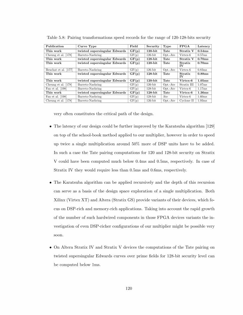
Table 5.8: Pairing transformations speed records for the range of 120-128-bits security
Publication Curve Type Field Security Type FPGA Latency
This work twisted supersingular Edwards GF(p) 120-bit Tate Stratix V 0.54ms
Cheung et al. [178] Barreto-Naehring GF(p) 126-bit Opt.-Ate Virtex-6 0.57ms
This work twisted supersingular Edwards GF(p) 128-bit Tate Stratix V 0.70ms
This work twisted supersingular Edwards GF(p) 120-bit Tate StratixIV
0.70ms
Beuchat et al. [177] Barreto-Naehring GF(p) 126-bit Opt.-Ate Virtex-6 0.83ms
This work twisted supersingular Edwards GF(p) 128-bit Tate StratixIV
0.88ms
This work twisted supersingular Edwards GF(p) 120-bit Tate Virtex-6 1.05ms
Cheung et al. [178] Barreto-Naehring GF(p) 126-bit Opt.-Ate Stratix III 1.07ms
Fan et al. [198] Barreto-Naehring GF(p) 128-bit Opt.-Ate Virtex-6 1.17ms
This work twisted supersingular Edwards GF(p) 128-bit Tate Virtex-6 1.36ms
Fan et al. [198] Barreto-Naehring GF(p) 128-bit Ate Virtex-6 1.60ms
Cheung et al. [178] Barreto-Naehring GF(p) 126-bit Opt.-Ate Cyclone II 1.93ms
very often constitutes the critical path of the design.
• The latency of our design could be further improved by the Karatsuba algorithm [129]
on top of the school-book method applied to our multiplier, however in order to speed
up twice a single multiplication around 50% more of DSP units have to be added.
In such a case the Tate pairing computations for 120 and 128-bit security on Stratix
V could have been computed much below 0.4ms and 0.5ms, respectively. In case of
Stratix IV they would require less than 0.5ms and 0.6ms, respectively.
• The Karatsuba algorithm can be applied recursively and the depth of this recursion
can serve as a basis of the design space exploration of a single multiplication. Both
Xilinx (Virtex XT) and Altera (Stratix GS) provide variants of their devices, which fo-
cus on DSP-rich and memory-rich applications. Taking into account the rapid growth
of the number of such hardwired components in those FPGA devices variants the in-
vestigation of even DSP-richer configurations of our multiplier might be possible very
soon.
• On Altera Stratix IV and Stratix V devices the computations of the Tate pairing on
twisted supersingular Edwards curves over prime fields for 128-bit security level can
be computed below 1ms.
120

Table 5.9: Software implementations of pairing on (single core) Intel Core i7 2.8 GHz
Beuchat et al. [177] Optimal-Ate over Baretto-Naehring
Security Multiplication F 2p Squaring F 2
p Miller Loop Final Exponentiation Total Latency [µs]
126-bit 435 342 1330000 1000000 2330000 0.83
Tate pairing over twisted supersingular Edwards curve
Security Multiplication Squaring Miller Loop Final Exponentiation Total Latency
80-bit 2344 1998 11753280 2493120 14246400 5.09
120-bit 5944 5463 69840602 12518598 82359200 29.41
128-bit 7507 6650 89556628 14337372 103894000 37.11
Table 5.8 demonstrates the fastest to date hardware architectures for pairing computa-
tions in the 120-128-bit range of security. The fastest to date coprocessor for the pairing
computations on pairing-friendly Barreto-Naehring curves over prime field was reported in
[178] (the fastest overall hardware accelerator for pairing at 128-bit security level was re-
ported for binary fields and it was described in [179]). The best variant of the coprocessor
from [178] was reported on Stratix III and Virtex-6 and the resource utilization vectors were
4233 ALUTs, 72 DSPs and 7032 slices, 32 DSPs, respectively.
The coprocessors, demonstrated in this work, require much more area. It is primarily due
to the fact that in order to provide the same security level the supersingular curves require
much larger arguments for any basic arithmetic operation (five to six times for a security
level in a range 120-128-bit). The most basic version of the multiplier, demonstrated in this
work, optimized for different DSP unit’s geometry, offers high computational power and a
big flexibility (double speed mode). A single multiplication unit, for 128-bit security level)
occupies already 88 DSP48e and 42 DSPs blocks for Virtex-6 and Stratix V, respectively.
On the other hand, the biggest advantage of this coprocessor is the fact that even though
that the major component, the multiplier is not using even more expensive Karatsuba-like
method, still it can compute pairing for the security range 120-128-bit within 541 µs on
28nm Stratix V. This result should be easily improved on any device with bigger number
of DSP units.
121

5.5.1 Note about software implementations
In the paper [177], the authors have presented a software library that implements the
optimal ate pairing over a Barreto-Naehrig curve at the 126-bit security level (very similar
to the work in [178]). The authors claim, it is ”the first (and the fastest so far) to have
reported the computation of a bilinear pairing at a level of security roughly equivalent to
that of AES-128 in less than one millisecond on a single core of an Intel Core i7 2.8GHz
processor”.
In this section we are going to provide a results of the software implementation of the
Tate pairing over twisted supersingular Edwards curve on prime fields at the 80, 120 and
128-bit security level at the same platform.
Our software library is written in C and can be used on several platforms, including
32/64-bit versions of Windows 7 with Visual Studio 2x Professional, Linux 2.6 and Mac
OS X 10.6 with gcc 4.2.1 or later, etc. Our implementation is based on the GMP library,
namely the arithmetic operations: modular addition, subtraction and multiplication use the
combination of mpz mod together with mpz add, mpz sub and mpz mul, respectively.
Table 5.9 summarizes the average latency in terms of time and clock cycles for full
pairing computations. Additionally, we have provided the implementation results for the
Miller loop, final exponentiation and basic arithmetic operations: modular multiplication
and squaring. For a range of security level 120-128-bit our Tate pairing is slower than the
Optimal-Ate pairing over Baretto-Naehring curves in a range of 30-40 times.
Taking into account three facts:
• the number of modular multiplications/squaring for 80, 120 and 128-bit security levels
are 5036, 10584 and 11148, respectively, and
• the number of clock cycles per modular multiplication/squaring for aforementioned
security levels are (2344, 1998), (5944, 5463) and (7507, 6650), respectively, and
• with a given total number of clock cycles for full pairing operation, summarized in
122

the column 6 of Table 5.9
we can estimate that those two basic arithmetic operations contribute to the full com-
putations of pairing in a range of 70-80%.
In order to provide a software implementation, being competitive to the implementation
results reported in [177], using the optimization techniques described in this chapter, every
modular multiplication/squaring have to be conducted below 200 clock cycles (approx. 30-
40 times faster than in GMP library). The other possibility would be a multi thread software
library for the Tate pairing over twisted supersingular Edwards curves.
5.6 Conclusions
In this chapter, we have demonstrated the very first hardware architecture of pairing on
Edwards curves. First, we have proposed, novel, low latency, a hybrid adder based on the
high-radix carry save addition and the Kogge-Stone adder. Based on this concept we have
developed new hardware architectures, optimized for FPGA devices, for modular addition,
subtraction and multiplication for Solinas primes.
We demonstrated that these circuits, together with proper high-level scheduling, is very
applicable for the pairing computations. The fastest version computes a Tate pairing at 80,
120 and 128-bit security over prime field in less than 0.13, 0.54 and 0.70 ms, respectively.
We must also admit that the proposed circuit seems to be relatively expensive in terms of
the area utilization.
For future work, we would like to further investigate the methods of area and latency
reduction in Edwards curves based pairings. One of possible direction, an implementation-
related, is the usage of hardwired macros instead of inferring embedded components in
FPGA devices.
Finally, we would like to investigate even higher security levels, and conduct the practical
experiments on Xilinx Virtex-6 and Altera Stratix-IV and V evaluation boards.
123

Part III
Benchmarking of FPGA-based
coprocessors for cryptography
124

Chapter 6: Benchmarking of hardware architectures for
Cryptography
A fair comparison of functionally equivalent digital system designs targeting FPGAs
is a challenging and time consuming task. The results of the comparison depend on
the inherent properties of competing algorithms, as well as on selected hardware ar-
chitectures, implementation techniques, FPGA families, languages and tools. In 2010
Cryptographic Engineering Research Group have introduced an open-source environ-
ment, called ATHENa for fair, comprehensive, automated, and collaborative hardware
benchmarking of algorithms belonging to the same class. In this chapter we are going to
demonstrate the heart of ATHENa, the most successful heuristic optimization algorithm
the GMU Optimization 1.
Contents
6.1 Introduction and motivation . . . . . . . . . . . . . . . . . . . . . 125
6.2 Previous work . . . . . . . . . . . . . . . . . . . . . . . . . . . . . 129
6.3 A heuristic optimization algorithm for FPGA-based hardware
architectures . . . . . . . . . . . . . . . . . . . . . . . . . . . . . . 133
6.4 Results . . . . . . . . . . . . . . . . . . . . . . . . . . . . . . . . . . 137
6.5 Conclusions . . . . . . . . . . . . . . . . . . . . . . . . . . . . . . . 139
6.1 Introduction and motivation
In almost every area of science and engineering, the same task can be realized using multiple
competing algorithms. This statement is especially true in case of communications, digital
125
signal processing, and cryptography. The choice of a particular algorithm depends strongly
on its efficiency in software and hardware.
In 2010 the Automated Tool for Hardware EvaluatioN (ATHENa) was proposed by
Cryptographic Engineering Research Group at George Mason University and originally
described in [199]. The improved version, still under development is presented in [200]. One
of the primary goals of this environment is to make the comparison of competing algorithms
fairer and more comprehensive, especially for the case where reconfigurable hardware is a
viable and advantages means of implementation. Although our environment can be used
for comparison of algorithms belonging to different fields, it is beneficial to focus first on
algorithms belonging to one particular area: cryptography.
6.1.1 Cryptographic Competitions
The reason why this area is appropriate include
• well documented speed-ups and security gains of FPGA implementations over software
implementations,
• constantly evolving standards, due to the everlasting struggle between designers of
new algorithms and cryptanalysts attempting to break them,
• strong need for fair evaluation associated with the way new cryptographic standards
are being developed, namely through open competition of algorithms submitted by
groups from all over the world. Starting from the Advanced Encryption Standard
(AES) contest organized by NIST in 1997-2000 [51], open contests have become a
method of choice for selecting cryptographic standards in the U.S. and over the world.
The AES contest in the U.S. was followed by the NESSIE competition in Europe [201],
CRYPTREC in Japan [202], and eSTREAM in Europe [203]. Recently, the focus of
attention of the entire cryptographic community was on the SHA-3 contest for a new
hash function standard, organized by NIST [41].
126

− 4 HW Winners
97 98 99 00 01 02 03 04 05 06 07 08 09 10 11 12 13 14 15 16 17 18
CAESAR
SHA−3
eSTREAM
NESSIE
CRYPTREC
AES
51 Candidates − 1 Winner
15 Candidates − 1 Winner
CRYPTREC, NESSIE − Multiple categories competitions
? Candidates − ? Winner(s)
34 Candidates − 4 SW Winners
96
Figure 6.1: Timeline of the major cryptographic competitions
Next in line is going to be the authenticated encryption competition - CAESAR [204].
Figure 6.1 demonstrates the timeline of cryptographic competitions.
Four typical criteria taken into account in the evaluation of candidates are: security,
performance in software, performance in hardware, and flexibility. While security is com-
monly recognized as the most important evaluation criterion, it is also a measure that is
most difficult to evaluate and quantify, especially during the relatively short period of time
reserved for the majority of contests. The typical outcome is that, after eliminating a frac-
tion of candidates based on security flaws, a significant number of remaining candidates
do not demonstrate any easy to identify security weaknesses, and as a result are judged to
have adequate security. Interestingly, the differences among the cryptographic algorithms
in terms of the hardware performance appeared to be particularly large, and often served
as a tiebreaker when other criteria failed to identify a clear winner in AES [205], [206],
eSTREAM [207], [208], and SHA-3 [93], [209].
127

6.1.2 Obstacles to a fair comparison
Saar Drimer in his PhD thesis [210] defined several problems related to benchmarking of
FPGA implementations of cryptographic transformations. The most important issues dis-
cussed in his dissertation were associated with the difficulties in results replication, selection
of the best set of design software options, and apple-to-orange comparison practices (dif-
ferent target technology, software version, etc). In the eve of SHA-3 contest this work was
a trigger for the development of automated FPGA benchmarking systems and hardware
evaluation methodologies.
Facilitating a fair and comprehensive comparison among competing cryptographic algo-
rithms, implemented in FPGA devices, was investigated in [21] and [211]. Corresponding
ASIC-oriented methodologies were proposed in [212], [209] and [213].
In order to conduct a fair comparison several obstacles have to be resolved. Most of
them are relatively simple to overcome:
• an influence of different hardware description languages: Either of the two
languages, VHDL or Verilog, is perfectly suited for the implementation and com-
parison of cryptographic transformations, as long as all competing algorithms are
described in the same language. Using two different languages to describe different
candidates may introduce an undesired bias to the evaluation.
• an influence of the designer skills: Re-usage of the recurring hardware compo-
nents and the small team of closely cooperating engineers can reduce significantly, a
so called ”human factor” in the optimization effort for a given hardware architecture.
• an influence of the selected platform: FPGA devices from two major vendors,
Xilinx and Altera, dominate the market with about 90% of the market share. There-
fore, we assume that it is appropriate to focus on FPGA devices from these two
companies.
• an ambiguity in the definition of our hardware cores: In order to define
128
hardware architectures for cryptographic transformations, and in order to make their
implementations as practical as possible, we have developed a FIFO-based interface
shown in Fig. 1a in [21]. It was proposed for hash functions, however it could be
easily adapted to other transformations.
• selection of performance evaluation metrics: In most of the cases (hash func-
tions, stream and block ciphers) our choice is the Throughput to Area Ratio, where
Throughput is defined as Throughput for long messages, and Area is expressed in
terms of the number of basic programmable logic blocks specific to a given FPGA
family. Optimizing for the best ratio provides a good balance between the speed and
the cost of the solution. However in case of transformations based on modular arith-
metic, the major performance related metric is the latency of basic operation. Due to
this fact the efficiency is typically defined as the latency · area.
• the selection of tools, their versions, and a set of the best options: For the
sake of selection of the best set of options for the CAD tools of major vendors, some
heuristic algorithms have to be developed.
This chapter demonstrates two algorithms for both Xilinx and Altera tools for the
selection of best options for the appropriate tools. To the best of our knowledge these are
two the best, to date, heuristic optimization strategies in this area.
The rest of this chapter is organized as follows:
In Section 6.2 we discuss previous work. Section 6.3 is devoted to the description of
the heuristic method the GMU Optimization 1. Section 6.4 demonstrates the list of major
successes of aforementioned algorithm, finally we draw conclusions in Section 6.5.
6.2 Previous work
FPGA vendors have recently started the development of tools for the exploration of im-
plementation options. The major FPGA vendors Xilinx and Altera publish their version
129
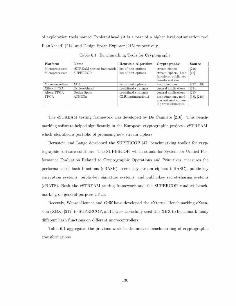
of exploration tools named ExploreAhead (it is a part of a higher level optimization tool
PlanAhead) [214] and Design Space Explorer [215] respectively.
Table 6.1: Benchmarking Tools for Cryptography
Platform Name Heuristic Algorithm Cryptography Source
Microprocessors eSTREAM testing framework list of best options stream ciphers [216]
Microprocessors SUPERCOP list of best options stream ciphers, hashfunctions, public keytransformations
[47]
Microcontrollers XBX list of best options hash functions [217], [48]
Xilinx FPGA ExploreAhead predefined strategies general applications [214]
Altera FPGA Design Space predefined strategies general applications [215]
FPGA ATHENa GMU optimization 1 hash functions, mod-ular arithmetic, pair-ing transformations
[38], [218]
The eSTREAM testing framework was developed by De Canniere [216]. This bench-
marking software helped significantly in the European cryptographic project - eSTREAM,
which identified a portfolio of promising new stream ciphers.
Bernstein and Lange developed the SUPERCOP [47] benchmarking toolkit for cryp-
tographic software solutions. The SUPERCOP, which stands for System for Unified Per-
formance Evaluation Related to Cryptographic Operations and Primitives, measures the
performance of hash functions (eBASH), secret-key stream ciphers (eBASC), public-key
encryption systems, public-key signature systems, and public-key secret-sharing systems
(eBATS). Both the eSTREAM testing framework and the SUPERCOP conduct bench-
marking on general-purpose CPUs.
Recently, Wenzel-Benner and Graf have developed the eXternal Benchmarking eXten-
sion (XBX) [217] to SUPERCOP, and have successfully used this XBX to benchmark many
different hash functions on different microcontrollers.
Table 6.1 aggregates the previous work in the area of benchmarking of cryptographic
transformations.
130

Automated Tool for Hardware EvaluatioN
to Device Resources
Place and RouteDesign Resources
Perform TimingAnalysis
Generate
Programming File
Project description
Translate Design Files
Heu
ristic Alg
orith
ms
XILINX ALTERA
quartus_map
quartus_fit
quartus_tan
quartus_asm
NGDBUILD
MAP
PAR
TRCE
BITGEN
Map Design Elements
Figure 6.2: Relation between design flows of Altera and Xilinxand heuristic algorithms in ATHENa
6.2.1 Automated Tool for Hardware EvaluatioN
A very first cross-FPGA platform for hardware benchmarking, Automated Tool for Hard-
ware EvaluatioN - ATHENa, has been proposed at George Mason University in 2010.
The major features of this software are:
• Running all steps of synthesis, implementation, and timing analysis in
batch mode (Fig. 6.2): This is a very important property, as it allows running time-
consuming optimizations, without any user supervision, over long periods of time,
such as nights, days, or even weeks.
• Support for devices and tools of two major FPGA vendors: Xilinx and
Altera: Xilinx and Altera account for about 90% of the FPGA market. Their FPGA
devices differ considerably in terms of the structure of a basic building block: con-
figurable logic block (CLB) for Xilinx, and logic element (LE) for Altera. They also
differ in terms of dedicated hardwired units, such as blocks of memory, multipliers,
131

DSP units, etc. As a result, the ranking of algorithms or architectures obtained using
devices of one FPGA vendor may not carry to the devices of another vendor.
• Generation of results for multiple FPGA families of a given vendor, (e.g.
Xilinx: Spartan 3, Virtex 5; Altera: Cyclone III, Aria II, Stratix IV): Our tool allows
specifying as target platforms multiple families of FPGA devices of each of the two
major vendors.
• Automated choice of a device within a given family of FPGAs assuming
that the resource utilization does not exceed a certain limits: A maximum
clock frequency of a circuit implemented using an FPGA is a function of device re-
source utilization. When the device utilization reaches 80+% in terms of one of the
critical resources, such as configurable logic blocks or Block RAMs, the performance
degrades. This effect is caused mostly by the difficulties associated with routing in
congested circuits. The utilization threshold at which the performance degradation
begins is a function of an FPGA family, an implemented circuit and the version of
the design tools.
• Automated verification of a design through functional simulation, run in
batch mode: Our tool has an additional capability of simulating designs in batch
mode in order to verify their correct functionality. The verification is based on a
testbench utilizing test vectors stored in a file, and providing a binary answer whether
the circuit operates correctly or not.
• Finally, Automated optimization of results aimed at one of the three opti-
mization criteria: speed, area, and ratio speed to area: Results generated by
the FPGA tools depend highly on the choice of multiple options and the contents of
constraint files. Variation of results obtained by changing just a single option may
easily exceed 25%. Currently, the most successful heuristic algorithm for throughput
and throughput to area ratio optimization is the GMU optimization 1 method.
132

6.3 A heuristic optimization algorithm for FPGA-based hard-
ware architectures
6.3.1 A case study and the design rationale for the best ATHENa heuris-
tic algorithm
Out of several hardware architectures of SHA-256, we have selected and implemented an
architecture referred to as architecture with rescheduling. It is an optimized architecture,
developed by Chaves et al. [219], optimized for the maximum throughput to area ratio. The
SHA-2 coprocessor design was adjusted to the evaluation methodology proposed in [21].
The synthesizable source codes, the testbench, and the specification of the generic in-
terface are all available at the ATHENa project web site [218]. For our experiments we
have then selected a 65nm Xilinx Virtex-5 device, xc5vlx30ff676-3, the smallest device in
this family, with the fastest speed grade (in this proposal we are not going to present our
design rationale for Altera devices).
Modern design flow for the FPGA devices is built upon multiple parameterizable steps.
The options available for the designer at every stage can be divided into three classes of
options:
• options with large space of possible values and their ranges unknown,
• options with large space of possibilities, but within fixed range, and
• the rest of available options with a few possible values - typically 2 or 3.
We have identified that the first group of the design software options is represented by
the requested frequency and the setting of a maximum fan-out of a logic gate (which is the
total number of gate inputs to which an output of a given gate is connected). The range of
possible values depends on the VHDL project description and the target device.
133

Table 6.2: Influence of design software options on implementation results for theoptimized architecture of SHA-256 by Chaves et al.
options improvement conclusions
frequency area:-7%, speed:31%,throughput/area:27%
high correlation between requested and achievedfrequency presented in Fig. 6.3
placement area:-7%, speed:6%,throughput/area:11%
the correlation between placement position andachieved frequency difficult to observe
other area:-1%, speed:17%,throughput/area:18%
The option: (effort level = high) improves re-sults, but requires more time for execution
The second group is represented by a starting point of a physical implementation. It is
denoted as the Cost Table value (1 to 100) in Xilinx Place and Route and the Seed value
(1 to 232 − 1) in case of Altera Quartus Fitter.
Finally, the remaining options can be very often represented by a simple flag. For in-
stance, the effort level, which particular design software is working on, can be set using
three values: HIGH, MEDIUM and NORMAL. Those implementation attempts with dif-
ferent effort levels are based on a simple trade-off between the higher quality results and
the execution time of the tools.
In Table 6.2 we have summarized the influence of various software options on the final
implementation results in case of each and every group of selected options.
6.3.2 Heuristic optimization algorithms for FPGA design flow
The highest generalization level of the proposed heuristic optimization method was the level
of the vendor’s specific design tools. Our heuristic strategy was named GMU Optimization 1
and it performs optimization specific to a Xilinx ISE and Altera Quartus.
For Xilinx, it combines an optimal requested frequency search, and placement search
with three different optimization targets (Area, Speed and Balanced), and an effort level
selection.
For Altera, only placement search and optimization target are combined together as not
much can be gained from frequency search.
The GMU optimization 1 heuristic method is demonstrated for Xilinx and Altera on
134

!"#$%#&'()"#*+,-.&
/+0#123
!"# !#$
" ! % & ' $ ( ) * "# "" "! "% "& "'
"##
"!#
"&#
"$#
")#
!##
!!#
+,-.,/0,1
2345,6,1
7+.8/
9+,-.,83:;<=>?@
Figure 6.3: Dependency between requested and achieved frequency for combinedoptimization targets
Figs. 6.4 and 6.5, respectively.
For Xilinx, the GMU Optimization 1 algorithm works as follows. For each of the op-
timization targets, an initial run (Run(Freq, Settings)) with default options of the design
tools is generated using the default options. The frequency achieved (Fach) in this initial
run determines the starting point of the frequency search. After this initial frequency value
is determined, the next run is executed with a requested frequency (Freq) equal to the last
achieved value increased by the percentage indicated by the first value (Fstep(0)) in the
predefined requested frequency improvement steps list (the size of this list is denoted as
ord(Fstep)). The result from this run is used as the starting point for the next run, and this
process is continued until either zero or negative improvement is generated by the design
software. Once the increases in requested frequency no longer yields a positive effect on the
achieved frequency, the highest achieved frequency is used as the requested frequency and
the design software options are set to a high effort (Settings=high effort).
The previous incremental improvement process is continued using the high effort options
until a positive effect on achieved frequency is no longer attainable. At this point the
algorithm will iterate through the placement options to try to accomplish a positive change
135

Settings = Default
Settings = High Effort
Y
N
Y
Stop
Y
N
Y
j = ord(Placement)N
j = j + 1
N
Y
Settings, Placement(j))
i=1, j=1
i = i + 1
j = 0
= DefaultFreq
achF = Run( Freq , Settings)
Freq = Fach +
Fach * Fstep
Fach = Run( Freq , Settings)
Fach Freq> Freq = Fach +
Fach * Fstep (0)/100
(0)/100
Fach = Run( Freq , Settings)
Fach > FreqFreq= Fach +
Fach * Fstep (0)/100
i = ord(F step )
reqF>achF
N
Fach = Run( Freq
+achF=reqF
(i)/100Fstep*achF
Figure 6.4: ATHENa GMU optimzation 1 method for Xilinx devices
in the achieved frequency. The placement options are determined by the number chosen for
Xilinx COST TABLE entry (Placement(j) for j ≥ 0). The initial incremental improvement
process is used again until no benefit from the requested frequency increase is observed.
At this point, the highest achieved frequency is used as the basis for incremental im-
provement, now using the step value indicated as the next value in the predefined requested
frequency improvement step list (Fstep(i) for i ≥ 0). This process continues until all values
within the list have been used.
In case of Altera, the GMU optimization 1 runs through the list of all possible place-
ments (Placement(i) for i ≥ 0) and through the list of all possible optimization targets
(optimization(b) for b=speed, area, balanced). The GMU optimization 1 is in fact the ex-
haustive search over a two-dimensional space (placement, optimization target).
136

j=ord(Placement)
N
Y
N j = j + 1
j = j + 1
Y
b=ord(optimization)
Stop
j = 0
b = b + 1N
Y
Settings = Default + optimization(b)
j = 0, b = 0
= Run(Settings, Placement(j))highestF
Settings = Default + optimization(b)
= Run(Settings, Placement(j))Fach
Fach > FhighestFhighest = Fach
Figure 6.5: ATHENa GMU optimzation 1 method for Altera devices
6.4 Results
The list of the papers, where the GMU Optimization 1 optimization strategy was used for
the results generation and optimization is already very long and it is expected to grow
quickly.
The first big test of our environment was its application to the evaluation of candi-
dates submitted to the SHA-3 contest for a new hash function standard, organized and
coordinated by NIST:
• The hardware architectures, optimized for throughput/area ratio and based on recon-
figurable logic only for 14 candidates of the 2nd round of the SHA-3 competition have
been reported in [21], [220] and [75]. To the best of our knowledge, ATHENa helped
to generate 11 out 14 best designs in terms of throughput/area ratio, outperforming
other designs reported earlier in the literature.
137

22
Relative Improvement of Results from Using ATHENa Virtex 5, 256-bit Variants of Hash Functions
0
0.5
1
1.5
2
2.5
Area Thr Thr/Area
Ratios of results obtained using ATHENa suggested options vs. default options of FPGA tools Figure 6.6: Relative improvement of results from using ATHENa Virtex 5, 256-bit
variants of hash functions. Ratios of results obtained using ATHENa suggested options vs.default options of FPGA tools. [21]
• Furthermore, it contributed to the improvement of 10 out 14 round two candidates,
when the hardwired components in modern FPGAs were used. The results presented
in [33] and [40] show that in case of AES-like hash functions improvement in terms of
the throughput/area ratio was able to reach even 100+%.
• In [221], [93] and [222], we have conducted the hardware architectures exploration
among five finalists of the SHA-3 competition. The results, reported in [221], are the
best reported in the literature for portable source codes (no low level components
used, e.g.: Xilinx Unisim library).
• Moreover, in case of the SHA-3 competition our optimization method have been proven
to be effective also for the designs, optimized for low area utilization, demonstrated in
[223] and [224].
Finally, the GMU Optimization 1 have been demonstrated to be applicable for different
types of transformations:
• Authenticated encryption based on the AES-Grøstl coprocessor, presented in [28] and
138

[29].
• Arithmetic and modular arithmetic cores, presented in [35] and [36].
• Pairing accelerators based on embedded resources, demonstrated in [36].
Typically, it is expected that the GMU Optimization 1 optimization algorithm will im-
prove the implementation results between 30 and 100% (Fig. 6.6).
6.5 Conclusions
The ATHENa and its heart, the GMU Optimization 1, optimization strategy, will continue
to serve the cryptographic and FPGA community for years to come, providing comprehen-
sive and easy to locate results for multiple cryptographic standards and other classes of
algorithms.
Researchers all over the world will benefit from the capability of fairly, comprehensively,
and automatically comparing their new algorithms, hardware architectures, and optimiza-
tion methods against any previously reported work. The designers will benefit from the
capability of comparing results of implementing the same algorithm using multiple FPGAs
from several major vendors, and will be able to make an informed decision about the choice
of the implementation platform most suitable for their particular application. The develop-
ers and users of tools will benefit from the comprehensive comparison done across tools from
various vendors, and from the optimization methodologies developed and comprehensively
tested as a part of this project.
139

Chapter 7: Conclusions and future research
In this chapter, we will provide a summary for this dissertation as well as several rec-
ommendations for future research.
Contents
7.1 Conclusions . . . . . . . . . . . . . . . . . . . . . . . . . . . . . . . 140
7.2 Future work . . . . . . . . . . . . . . . . . . . . . . . . . . . . . . . 144
7.1 Conclusions
In this research, we have made an effort to answer a critical question whether the emerging
cryptographic transformations (such as SHA-3 finalists and Tate pairing based on Edwards
curves) can be used to develop the most efficient to date hardware architectures of cryptog-
raphy taking full advantage of special embedded resources present in modern FPGAs.
Hardware architectures investigated in this research contribute to the five, most impor-
tant cryptographic services: confidentiality, integrity, authentication, non-repudiation, and
key exchange. The thesis is divided into three major parts, describing our original contribu-
tions to the areas of: high-performance architectures supporting confidentiality, integrity,
and authentication, hardware architectures supporting key exchange and non-repudiation,
and algorithms for benchmarking and optimization of FPGA-based coprocesors for cryp-
tography.
In the first part, we have discussed new hardware architectures for the emerging hash
functions (used as a basis of integrity, authentication, and non-repudiation services) devel-
oped during the SHA-3 contest held by NIST in the period 2007-2012. In particular, we
140

have concentrated on the AES-inspired class of hash functions that advanced to the Round
2 of the competition, including ECHO, Fugue, Grøstl-0, and SHAvite-3. We have proven
that these functions can benefit from the special T-box hardware architecture, inspired by a
somewhat similar hardware architecture of AES. The proposed architecture has been shown
to improve the throughput to area ratio of the four aforementioned hash functions by 49,
173, 424 and 262%, respectively. More importantly, by applying the same technique, the
performance of the SHA-3 finalist Grøstl has been improved by 446%, 158% and 58% in
Cyclone II, Stratix III, and Virtex 5, FPGAs, respectively. As a second major contribution,
we have proposed a new joint architecture for Grøstl and AES, supporting the use of these
two algorithms for authentication and confidentiality, respectively, in secure Internet pro-
tocols, such as IPSec. This architecture allows substantial resource sharing between Grøstl
and AES. Our coprocessor based on this architecture outperforms the best earlier reported
design by Jarvinen et al. by 64% for the IP ESP (Encapsulating Security Payload) protocol
being a heart of IPSec.
In the second part of the thesis, we focus on new hardware architectures, for emerging
public key cryptosystems, such as pairing based schemes. In particular, we investigate in
detail the Tate pairing transformation over Edwards curves. To the best of our knowl-
edge, this particular transformation has never been implemented in hardware. In order to
support cryptographic services such as confidentiality, non-repudiation, and key exchange,
the emerging Pairing-based Cryptography provides unique cryptographic mechanisms, such
as Identity-based encryption, Identity-based signatures, and One-Round Tri-Partite key-
exchange. Our FPGA-based coprocessor, which can be used directly in any of the afore-
mentioned schemes, demonstrates that pairing over Edwards curves is a very promising
direction, which should be further investigated from the point of view of standardization
and efficient implementations in software and hardware. In particular, we have demon-
strated, that even though Edwards curves were not optimized for pairing, they present
a valid alternative to pairing friendly Barreto-Naehrig curves. By implementing our new
hardware architecture on Altera Stratix V, we have shown that our solution outperforms
141

all previously reported FPGA-based pairing coprocessors operating over prime fields, for
the security level between 120 and 128 bits.
In order to accomplish this result, we have made several important contributions at the
intersection of cryptography and computer arithmetic. In particular, we have developed:
• a new, low latency adder based on the use of high-radix carry save representation
and Parallel Prefix Networks. We have demonstrated that for long operands, exceed-
ing 1024 bits, this adder takes the best advantage of the special embedded resources
supporting fast addition in modern FPGAs called fast carry chains. Our design out-
performs the best classical fast adders, Kogge-Stone and Brent-Kung, in terms of the
latency · area product by up to 50, 38 and 35% for 1024, 2048 and 4096-bit operands,
respectively. At the same time it matches or outperforms these adders in terms of
latency.
• a new, low latency modular adder/subtractor based on the aforementioned adder.
This modular adder has been shown to significantly outperform all previously known
designs in terms of both latency and the product of latency · area. In terms of both of
these performance measures an average improvement over the best of the two classical
designs was shown to be 15, 40 and 55% for Altera devices, and 50, 45 and 70% for
Xilinx devices. The three numbers listed above refer to the results for the 1024,
2048, and 4096-bit operands, respectively. As can be seen from these results, the
improvement increases with the increase in the size of operands, which makes this
modular adder particularly attractive for the entire field of public key cryptography,
in which key sizes and thus operand sizes tend to increase over time to compensate
for the constant progress in cryptanalysis and computing power.
• a new, low latency grid multiplier based on the used of DSP units of modern FPGAs.
This multiplier incorporates the best features of the previously reported multipli-
ers, removes some of their restrictions (such as a focus on RSA and Diffie-Hellman
schemes), and supports the double speed mode of operation for the case when the
142

number of available multipliers exceeds the number of multiplications that can be
scheduled at the same time.
• a new, low latency modular multiplier based on the used of DSP units of modern
FPGAs, optimized for the case of special primes used in cryptography called Solinas
primes. Our solution takes advantage of the Barrett reduction, which replaces division
by multiplication, and of the special form of intermediate operands, which allows
replacing multiplication by multi-operand addition. To the best of our knowledge this
approach has been applied for the first time to the case of Tate pairing over Edwards
curves, and it can be generalized to other related classes of public key cryptosystems.
Finally, in the third part of our thesis, we have described our contribution to the open-
source environment, called ATHENa, for fair, comprehensive, automated, and collaborative
benchmarking and optimization of digital system designs targeting modern FPGAs. We
have developed the heart of ATHENa, the most successful heuristic optimization algorithm:
GMU Optimization 1. This algorithm has been shown to allow overall improvements in
terms of the throughput to area ratio in the range of 100%. Additionally, this algorithm has
been shown to be general enough to apply to several different classes of digital circuits: hash
functions, secret key ciphers, modular arithmetic on long operands, pairing transformations,
etc. So far, it has served as a back-end tool for the result generation in at least ten
publications.
Based on the obtained results and the presented contributions, we may conclude that the
emerging cryptographic transformations investigated in this thesis, namely AES-based SHA-
3 candidates and the Tate pairing on Edwards curves, are well suited for implementation
using modern FPGAs, and can take advantage of special computational units embedded in
these FPGAs. Combining the power of new algorithms and the power of new FPGAs leads
to some of the most efficient implementations of cryptography reported in the literature to
date.
143

7.2 Future work
There are several possible approaches for the extension of this work. This section is devoted
to some of the directions in which the problems can be further explored.
7.2.1 Hardware architectures for pairing on ordinary Edwards curves
The hardware acceleration of pairing on supersingular twisted Edwards curves over prime
fields has occurred to be very fast, yet also very demanding in terms of area. Our initial
results of the hardware acceleration of pairing on ordinary Edwards curves, defined in [180],
has revealed that this algorithm will require approximately fifteen times fewer reconfigurable
resource with two times longer computations. Therefore, in terms of the latency · area
product, this approach would lead to the improvement by a factor of seven and a half.
Additionally, our early investigation of data dependencies in the scheduling of the basic
building operations in pairing on ordinary Edwards curves, showed that it might be impos-
sible to bridge the gap in terms of latency for the pairing computations on supersingular
and ordinary Edwards curves. Thus, more research and a new approach might be necessary
to overcome this problem.
7.2.2 Hardware architectures for the Edwards Curves Digital Signature
Algorithm based on P25519
The Solinas primes, investigated in Chapter IV and V, were selected in a such a way that
their µ = 22n
p parameter consists of a relatively small number of terms (<30). The prime
2255 − 19 (also called P25519), originally defined by Bernstein in [225], has very similar
hardware-friendly properties. Both p and µ parameters for P25519, required in the Barrett
reduction [128], consist of relatively small number of terms.
Bernstein et al. [226] have reported the fastest, to date, software implementation of
144

Digital Signature Algorithm based on Edwards curves (so called EdDSA) and P25519. Due
to the similarities, in regards to the Barrett reduction parameters, between the hardware
architectures of Solinas primes arithmetic and the P25519 arithmetic, we believe that using
our novel architectures for modular arithmetic on large integers it should be possible to
build the fastest to date hardware coprocessor for the ECDSA [227].
7.2.3 Hardware architectures for the short digital signatures based on
the Barreto-Naehrig curves
Currently, the shortest digital signatures are offered by pairing transformations. The shorter
signatures the smaller requirements for the storage and the transmission time of this crucial
information. This feature is especially important in resource constrained environments,
where the power consumption used for transmission of data is often the most limiting
factor [228]. In order to reduce the size of a digital signature by half, without compromising
its security a new technology has to be used. One of the first, proposed in the literature
short signature schemes is the Boneh-Lynn-Shacham (BLS) scheme [168].
Based on the current state of knowledge, the most suitable, for the short digital sig-
natures, are the Barreto-Naehrig curves [187]. For the 128-bit security level the Barreto-
Naehrig-based BLS scheme produces 256-bit digital signatures. Contrary, the BLS scheme,
based on supersingular and ordinary Edwards curves, produces 1493 and 401-bit digital
signatures, respectively. Thus, the optimal selection for the short digital signatures are the
Barreto-Naehrig curves. We believe that the implementation of pairing on the Barreto-
Naehrig curves can be still improved using selected architectures presented in this thesis.
145

7.2.4 Hardware-Software co-design for Public Key Cryptography
A very complex system, which accommodates the functionality of Pairing-based Cryptog-
raphy, Elliptic Curve Cryptography, classical Public Key Cryptography or even symmet-
ric Cryptography, requires finding the correct balance between flexibility and performance.
Principles of a modern approach for such problems, so called, Hardware/Software Co-design
are described in [229]. Taking into account this technique, several directions are possible.
We name here two of them:
1. Due to the fact that different cryptographic algorithms, in order to provided the
same level of security, require different sizes of operands (e.g.: for the 128-bit security
level: RSA, pairing on supersingular curves, ECDSA, pairing on ordinary Edwards
curves, pairing on BN-curves require 3072, 1493, 512, 401 and 256-bit operands respec-
tively), a hardware/software co-design is a highly attractive solution. A single scalable
multiplier, providing support for different sizes of arguments should be the primary
hardware element in such a system. All the high-level functionality: scheduling of the
arithmetic units for the basic iterative tasks of the aforementioned schemes or even
high level protocols and applications could be designed using software approach.
Such approach would provide, very strong alternative for the purely software or the
purely hardware oriented designs. It would inherit the natural software flexibility, but
also preserve some fraction of the hardware powerful computational features.
2. Partial Reconfiguration [230] is a technique that allows certain portions of an FPGA
device to be re-configured during run-time without affecting the functionality of other
portions of the system. This technique, together with an efficient use of hardware-
software co-design opens the door to the world of extreme efficiency of systems based
on FPGAs. Thanks to the utilization of both methods it might be possible to save a
significant portion of hardware resources with a relatively small penalty in terms of
performance. The aforementioned arithmetic support for cryptographic services could
be extended in a such a way, that instead of utilizing one generic, scalable modular
146
multiplier, we could have multiple application-optimized versions of arithmetic units.
Our joint work with Ahmad Salman and Jens-Peter Kaps [89] has revealed big poten-
tial for such systems. Typically, the latency of the cryptographic transformations for
the asymmetric cryptography is much larger than for the symmetric transformations
at the same security level, thus the overhead from the reconfiguration time contributes
less to the total response time in such a system.
147

Bibliography
148

Bibliography
[1] K. Jarvinen, “Sharing resources between AES and the SHA-3 second round candidatesFugue and Grøstl.”
[2] J. Daemen, “Cipher and hash function design. strategies based on linear and differ-ential cryptanalysis,” Ph.D. dissertation, Katholieke Universiteit Leuven, 1995.
[3] V. Rijmen, J. Deamen, B. Preneel, A. Bosselaers, and E. De Win, “The cipher shark,”in 3rd International Workshop on Fast Software Encryption FSE., 1996, pp. 99–111.
[4] J. Daemen, L. Knudsen, and V. Rijmen, “The block cipher square,” in Fast SoftwareEncryption (FSE), 1997.
[5] Advanced Encryption Standard (AES), National Institute of Standards and Technol-ogy (NIST), FIPS Publication 197, Nov 2001, http://csrc.nist.gov/publications/fips/fips197/fips-197.pdf.
[6] E. Biham, R. Anderson, and L. Knudsen, “Serpent: A new block cipher proposal,” inFast Software Encryption, FSE 1998, ser. Lecture Notes in Computer Science (LNCS),vol. 1372. Springer, January 1998, pp. 222–223.
[7] B. Schneier, J. Kelsey, D. Whiting, D. Wagner, C. Hall, and N. Ferguson, “Twofish: A128-bit block cipher,” Counterpane Systems, Minneapolis, MN, USA, AES Proposal,June 1998.
[8] E. Hong, J.-H. Chung, and C. H. Lim, “Hardware design and performance estimationof the 128-bit block cipher crypton,” in Workshop on Cryptographic Hardware andEmbedded Systems - CHES, 1999.
[9] T. Corp., “Specification of hierocrypt-3,” NESSIE.
[10] P. Barreto and V. Rijmen, “The khazad legacy-level block cipher,” First open NESSIEWorkshop, 2000.
[11] ——, “The anubis block cipher,” NESSIE, 2000.
[12] J. Borst, “The block cipher: Grand cru,” NESSIE, 2000.
[13] L. McBride, “Q - a proposal for nessie,” NESSIE, 2000.
[14] J. Daemen, M. Peeters, G. Van Assche, and V. Rijmen, “Nessie proposal: Noekeon,”2000.
149

[15] R. Benadjila, O. Billet, H. Gilbert, G. Macario-Rat, T. Peyrin, M. Robshaw, andY. Seurin, “SHA-3 proposal: ECHO,” Submission to NIST (updated), Feb 2009,http://crypto.rd.francetelecom.com/echo/.
[16] S. Halevi, W. E. Hall, and C. S. Jutla, “The hash function Fugue,” Submission to NIST(updated), Sep 2009, http://domino.research.ibm.com/comm/research projects.nsf/pages/fugue.index.html.
[17] P. Gauravaram, L. Knudsen, K. Matusiewicz, F. Mendel, C. Rechberger, M. Schaffer,and T. Søren, “Grøstl - a SHA-3 candidate,” Submission to NIST (Round 3), 2011.
[18] E. Biham and O. Dunkelman, “The SHAvite-3 hash function,” Submission to NIST(Round 2), 2009, http://www.cs.technion.ac.il/∼orrd/SHAvite-3/Spec.15.09.09.pdf.
[19] H. Wu, “The hash function JH,” Submission to NIST (round 3), 2011, http://www3.ntu.edu.sg/home/wuhj/research/jh/jh round3.pdf.
[20] J.-L. Beuchat, “Some Modular Adders and Multipliers for Field Programmable GateArrays,” in Parallel and Distributed Processing Symposium, 2003.
[21] K. Gaj, E. Homsirikamol, and M. Rogawski, “Fair and comprehensive methodologyfor comparing hardware performance of fourteen round two SHA-3 candidates usingFPGA,” in Cryptographic Hardware and Embedded Systems, CHES 2010, ser. LNCS,S. Mangard and F.-X. Standaert, Eds., vol. 6225. Springer Berlin / Heidelberg, 2010,pp. 264–278.
[22] A. J. Menezes, P. C. van Oorschot, and S. Vanstone, Handbook of Applied Cryptogra-phy. CRC Press Inc., 1997.
[23] W. Diffie and M. E. Hellman, “New directions in cryptography,” IEEE Transactionson Information Theory, vol. IT-22, no. 6, pp. 644–654, Nov 1976.
[24] R. L. Rivest, A. Shamir, and L. Adleman, “A method for obtaining digital signaturesand public-key cryptosystems,” Commun. ACM, vol. 21, no. 2, pp. 120–126, Feb 1978.
[25] X. Wang, Y. Yin, and H. Yu, “Finding collisions in the full sha-1,” in Advances inCryptology - CRYPTO, 2005.
[26] B. Brumley and N. Tuveri, “Remote timing attacks are still practical,” http://eprint.iacr.org/2011/232.pdf.
[27] V. S. Miller, “Short programs for functions on curves,” 1985,http://crypto.stanford.edu/miller/miller.pdf.
[28] M. Rogawski and K. Gaj, “A High-Speed Unified Hardware Architecture for AES andthe SHA-3 Candidate Grøstl,” in 15th EUROMICRO Conference on Digital SystemDesign – DSD’12, 2012.
[29] M. Rogawski, K. Gaj, and E. Homsirikamol, “A high-speed unified hardware architec-ture for 128 and 256-bit security levels of aes and grøstl,” Embedded Hardware Design:Microprocessors and Microsystems, 2013.
150
[30] S. Drimer, T. Guneysu, and C. Paar, “DSPs, BRAMs and a pinch of logic: Extendedrecipes for AES on FPGAs,” ACM Trans. Reconfigurable Technol. Syst. (TRETS),vol. 3, no. 1, pp. 1–27, 2010.
[31] V. Fisher and M. Drutarovsky, “Two methods of rijndael implementation in reconfig-urable hardware,” in Cryptographic Hardware and Embedded Systems CHES, 2001.
[32] S. Shah, R. Velegalati, J.-P. Kaps, and D. Hwang, “Investigation of DPA resistance ofBlock RAMs in cryptographic implementations on FPGAs,” in International Confer-ence on ReConFigurable Computing and FPGAs – ReConFig’10. IEEE, Dec 2010,pp. 274–279.
[33] M. U. Sharif, R. Shahid, M. Rogawski, and K. Gaj, “Use of embedded FPGA re-sources in implementations of five round three SHA-3 candidates,” ECRYPT II HashWorkshop, 2011.
[34] M. Rogawski, “Analysis of implementation of hierocrypt3 algorithm (and its compar-ison to camellia algorithm) using altera devices,” Biuletyn WAT, vol. 4, no. 620, Apr.2004, first version available on http://eprint.iacr.org/2003/258.
[35] M. Rogawski, K. Gaj, and E. Homsirikamol, “Fpga-based adder for thousand bitsand more,” in submitted to 2013 International Conference on Field ProgrammableTechnology - FPT, Dec 2013.
[36] M. Rogawski and K. Gaj, “Hardware acceleration for the tate pairing on supersingularedwards curves,” Journal of Cryptographic Engineering, 2013, submitted.
[37] M. P. L. Das and P. Sarkar, “Pairing computation on twisted Edwards form ellipticcurves,” in Pairing-Based Cryptography, 2008.
[38] K. Gaj, J.-P. Kaps, V. Amirineni, M. Rogawski, E. Homsirikamol, and B. Y. Brewster,“ATHENa – Automated Tool for Hardware EvaluatioN: Toward fair and comprehen-sive benchmarking of cryptographic hardware using FPGAs,” in 20th InternationalConference on Field Programmable Logic and Applications - FPL 2010. IEEE, 2010,pp. 414–421, winner of the FPL Community Award.
[39] E. Homsirikamol, M. Rogawski, and K. Gaj, “Throughput vs. area trade-offs archi-tectures of five Round 3 SHA-3 candidates implemented using Xilinx and Altera FP-GAs,” in Workshop on Cryptographic Hardware and Embedded Systems CHES 2011,ser. LNCS, B. Preneel and T. Takagi, Eds., vol. 6917. Springer Berlin / Heidelberg,Sep 2011, pp. 491–506.
[40] R. Shahid, M. U. Sharif, M. Rogawski, and K. Gaj, “Use of embedded FPGA resourcesin implementations of 14 Round 2 SHA-3 candidates,” in The 2011 InternationalConference on Field-Programmable Technology, FPT 2011, Dec. 2011.
[41] SHA3, “Cryptographic Hash Algorithm Competition,” http://csrc.nist.gov/groups/ST/hash/sha3/index.html, 2007.
[42] Secure Hash Standard (SHS), National Institute of Standards and Technology (NIST),Oct. 2008, http://csrc.nist.gov/publications/fips/fips180-3/fips180-3 final.pdf.
151
[43] SHA3-ZOO, “SHA-3 Hardware Implementations,” http://ehash.iaik.tugraz.at/wiki/SHA-3\ Hardware\ Implementations, 2009.
[44] GMU-CERG, “ATHENa Project website,” http://cryptography.gmu.edu/athenadb/,2010.
[45] G. Bertoni, J. Daemen, M. Peeters, and G. Van Assche, “The Keccak SHA-3 submission,” Submission to NIST (Round 3), 2011, http://keccak.noekeon.org/Keccak-submission-3.pdf.
[46] S.-j. Chang, R. Perlner, W. E. Burr, , M. S. Turan, J. M. Kelsey, S. Paul, andL. E. Bassham, “Third-Round Report of the SHA-3 Cryptographic Hash AlgorithmCompetition,” National Institute of Standards and Technology (NIST), Tech. Rep.,2012.
[47] D. J. Bernstein and T. Lange, “System for unified performance evaluation relatedto cryptographic operations and primitives,” ONLINE, 2006, http://bench.cr.yp.to/supercop.html.
[48] C. Wenzel-Benner and J. Graf, “eXternal Benchmarking eXtension (xbx),” ONLINE,2010, http://xbx.das-labor.org/trac.
[49] Advanced Encryption Standard (AES), National Institute of Standards and Technol-ogy (NIST), FIPS Publication 197, Nov 2001, http://csrc.nist.gov/publications/fips/fips197/fips-197.pdf.
[50] Data Encryption Standard (DES), National Institute of Standards and Technol-ogy (NIST), FIPS Publication 46-3, Oct 1999, http://csrc.nist.gov/publications/fips/fips46-3/fips46-3.pdf.
[51] NIST, “Aes archive,” http://csrc.nist.gov/archive/aes/, 2000.
[52] TrueCrypt Foundation, “Truecrypt,” http://www.truecrypt.org/, 2012.
[53] Weeny Software, “Truecrypt,” http://www.weenysoft.com/password-encryption-serpent.html, 2012.
[54] B. Schneier, “Twofish based products,” http://www.schneier.com/twofish-products.html, 2000.
[55] R. L. Rivest, “Block encryption algorithm with data-dependent rotations,” U.S.Patent 5724428, Mar. 1998.
[56] A. Schorr and M. Lukowiak, “Skein Tree Hashing on FPGA,” in Proc. ReConFig’10,2010, pp. 292–297.
[57] K. Guo and H. M. Heys, “A pipelined implementation of the grøstl hash algorithmand the advanced encyption standard,” in Canadian Conference on Electrical andComputer Engineering (CCECE 2013), 2013.
[58] N. At, J.-L. Beuchat, and I. San, “Compact Implementation of Threefish and Skeinon FPGA,” in Proc. NTMS, 2012.
152

[59] N. At, J.-L. Beuchat, E. Okamoto, I. San, and T. Yamazaki, “A low-area unifiedhardware architecture for the AES and the cryptographic hash function Grøstl,” http://eprint.iacr.org/2012/535, Sep 2012.
[60] M. Pelnar, M. Muehlberghuber, and M. Hutter, “Putting together what fits together- græstl,” in 11th International Conference, CARDIS 2012,, 2012.
[61] J.-L. Beuchat, E. Okamoto, and T. Yamazaki, “A low-area unified hardware archi-tecture for the AES and the cryptographic hash function ECHO,” Journal of Cryp-tographic Engineering, vol. 1, no. 2, pp. 101–121, 2011.
[62] J. Daemen and V. Rijmen, The Design of Rijndael. Springer Verlag, 2002.
[63] RFC-6101, “http://www.ietf.org/rfc/rfc6151.txt,” 2011.
[64] RFC-5246, “http://www.ietf.org/rfc/rfc5246.txt,” 2008.
[65] RFC-4251, “http://www.ietf.org/rfc/rfc4251.txt,” 2006.
[66] RFC-4301, “http://www.ietf.org/rfc/rfc4301.txt,” 2005.
[67] RFC-4308, “http://www.ietf.org/rfc/rfc4308.txt,” 2005.
[68] RFC-4309, “http://www.ietf.org/rfc/rfc4309.txt,” 2005.
[69] P. Gauravaram, L. Knudsen, K. Matusiewicz, F. Mendel, C. Rech-berger, M. Schlffer, and S. Thomsen, “Tweaks on grostl,” 2011,http://www.groestl.info/Round3Mods.pdf.
[70] P. Gauravaram, L. R. Knudsen, K. Matusiewicz, F. Mendel, C. Rechberger,M. Schaffer, and S. S. Thomsen, “Grøstl – a SHA-3 candidate,” Submission to NIST,Oct 2008, http://www.groestl.info/.
[71] M. Rogawski and K. Gaj, “Grøstl Tweaks and their Effect on FPGA Results,” Dec.2011, http://eprint.iacr.org/2011/635.pdf.
[72] S. Tillich, M. Feldhofer, M. Kirschbaum, T. Plos, J.-M. Schmidt, and A. Szekely,“High-speed hardware implementations of BLAKE, Blue Midnight Wish, CubeHash,ECHO, Fugue, Grøstl, Hamsi, JH, Keccak, Luffa, Shabal, SHAvite-3, SIMD, andSkein,” Cryptology ePrint Archive, Report 2009/510, Nov 2009, http://eprint.iacr.org/.
[73] L. Dadda, M. Macchetti, and J. Owen, “The design of a high speed ASIC unit for thehash function SHA-256 (384, 512),” in Proc. DATE’04, vol. 3, 2004.
[74] M. Macchetti and L. Dadda, “Quasi-pipelined hash circuits,” in Proc. ARITH’17,2005, pp. 222–229.
[75] E. Homsirikamol, M. Rogawski, and K. Gaj, “Comparing hardware performance offourteen round two SHA-3 candidates using FPGAs,” Cryptology ePrint Archive,Report 2010/445, 2010.
153

[76] B. Jungk and S. Reith, “On fpga-based implementations of the sha-3 candidategrøstl,” in International Conference on Reconfigurable Computing (ReConFig), Dec2010, pp. 316 – 321.
[77] S. Matsuo, M. Knezevic, P. Schaumont, I. Verbauwhede, A. Satoh, K. Sakiyama, andK. Ota, “How can we conduct “fair and consistent” hardware evaluation for SHA-3candidate?” Second SHA-3 Candidate Conference, Tech. Rep., 2010.
[78] B. Baldwin, N. Hanley, M. Hamilton, L. Lu, A. Byrne, M. O’Neill, and W. P. Mar-nane, “FPGA implementations of the round two SHA-3 candidates,” in 2nd SHA-3Candidate Conference, 2010.
[79] K. Kobayashi, J. Ikegami, S. Matsuo, K. Sakiyama, and K. Ohta, “Evaluation ofhardware performance for the SHA-3 candidates using SASEBO-GII,” http://eprint.iacr.org/2010/010, 2010.
[80] X. Guo, S. Huang, L. Nazhandali, and P. Schaumont, “On the impact of targettechnology in SHA-3 hardware benchmark rankings,” 2010, http://eprint.iacr.org/2010/536.pdf.
[81] K. Gaj, E. Homsirikamol, M. Rogawski, R. Shahid, and M. U. Sharif, “Comprehensiveevaluation of high-speed and medium-speed implementations of five sha-3 finalistsusing xilinx and altera fpgas,” Cryptology ePrint Archive, Report 2012/368, 2012,http://eprint.iacr.org/.
[82] Algotronix, “http://www.algotronix-store.com/,” 2008.
[83] Helion, “http://www.heliontech.com/,” 2011.
[84] M.-Y. Wang, H. C.-T. Su, Chih-Pin, and C.-W. Wu, “An HMAC processor withintegrated SHA-1 and MD5 algorithms,” in Proc. ASP-DAC’04, 2004, pp. 456–458.
[85] K. Jarvinen, M. Tommiska, and J. Skytta, “A compact MD5 and SHA-1 co-implementation utilizing algorithms similarities,” in Proc. ERSA’05, 2005, pp. 48–54.
[86] D. Cao, J. Han, and X.-Y. Zeng, “A reconfigurable and ultra low-cost VLSI imple-mentation of SHA-1 and MD5 functions,” in Proc. ASICON’07, 2007, pp. 862–865.
[87] T.-S. N. Chiu-Wah Ng and K.-W. Yip, “A unified architecture of MD5 and RIPEMD-160 hash algorithms,” in Proc. ISCAS’04, vol. 2, 2004.
[88] T. Ganesh, M. Frederick, T. Sudarshan, and A. Somani, “Hashchip: A shared-resourcemulti-hash function processor architecture on FPGA,” Integration, the VLSI journal,vol. 40, pp. 11–19, 2007.
[89] A. Salman, M. Rogawski, and J.-P. Kaps, “Efficient hardware accelerator for IPSECbased on partial reconfiguration on Xilinx FPGAs,” in ReConFig’11, 2011, pp. 242–248.
[90] N. At, J.-L. Beuchat, E. Okamoto, I. San, and T. Yamazaki, “A low-area uniedhardware architecture for the aes and the cryptographic hash function grøstl,” 2012,report 2012/535, 2012.
154

[91] J.-L. Beuchat, E. Okamoto, and T. Yamazaki, “A low-area unified hardware archi-tecture for the AES and the cryptographic hash function ECHO,” Cryptology ePrintArchive, Report 2011/078, Sep 2012.
[92] P. Gauravaram, L. R. Knudsen, K. Matusiewicz, F. Mendel, C. Rechberger,M. Schaffer, and S. S. Thomsen, “Grøstl – a SHA-3 candidate,” Submission to NIST,Oct 2008, http://www.groestl.info/.
[93] K. Gaj, E. Homsirikamol, M. Rogawski, R. Shahid, and M. U. Sharif, “ComprehensiveEvaluation of High-Speed and Medium-Speed Implementations of Five SHA-3 Final-ists Using Xilinx and Altera FPGAs,” Mar 2012, third SHA-3 candidate conference.
[94] G. CERG, “GMU SHA-3 source codes,” ONLINE, 2011, http://cryptography.gmu.edu/athena/index.php?id=source codes.
[95] NIST, The Keyed-Hash Message Authentication Code HMAC, National Institute ofStandards and Technology (NIST), FIPS Publication 198–1, Jul. 2008, http://csrc.nist.gov/publications/fips/fips198-1/FIPS-198-1 final.pdf.
[96] RFC-2104, “http://www.ietf.org/rfc/rfc2104.txt,” 1997.
[97] RFC-6151, “http://www.ietf.org/rfc/rfc6151.txt,” 2011.
[98] M. Dworkin, NIST Special Publication 800-38A: Recommendation for Block Ci-pher Modes of Operation, 2001, http://csrc.nist.gov/publications/nistpubs/800-38a/sp800-38a.pdf.
[99] Hardware Interface of a Secure Hash Algorithm (SHA), v. 1.4 ed., CryptographicEngineering Research Group, George Mason University, Jan 2010.
[100] K. Parhi, VLSI digital signal processing systems: design and implementation. JohnWiley & Sons, 1999.
[101] J. E. Bresenham, “Algorithm for computer control of a digital plotter,”IBM Syst. J., vol. 4, no. 1, pp. 25–30, Mar. 1965. [Online]. Available:http://dx.doi.org/10.1147/sj.41.0025
[102] X. Wu, “An efficient antialiasing technique,” SIGGRAPH Comput. Graph., vol. 25,no. 4, pp. 143–152, Jul. 1991. [Online]. Available: http://doi.acm.org/10.1145/127719.122734
[103] Secure Hash Standard (SHS), National Institute of Standards and Technology (NIST),Oct. 2008, http://csrc.nist.gov/publications/fips/fips180-3/fips180-3 final.pdf.
[104] X. Lai and J. L. Massey, “A proposal for a new block encryption standard,” inAdvances in Cryptology - EuroCrypt ’90, ser. Lecture Notes in Computer Science(LNCS), I. B. Damgard, Ed., vol. 473. Berlin: Springer-Verlag, 1990, pp. 389–404.
[105] P. Montgomery, “Modular multiplication without trial division,” Math. Comp.,vol. 44, no. 170, pp. 519–521, 1985.
155

[106] A. F. Tenca and c. K. Koc, “A scalable architecture for montgomery multiplication,”in Workshop on Cryptographic Hardware and Embedded Systems (CHES99), ser. Lec-ture Notes in Computer Science, C. Paar and c. K. Koc, Eds., vol. 1717. Heidelberg:Springer-Verlag, 1999, pp. 94–108.
[107] D. Harris, R. Krishnamurthy, M. Anders, S. Mathew, and S. Hsu, “An improvedunified scalable radix-2 montgomery multiplier,” in Computer Arithmetic, 2005.
[108] M. Huang, K. Gaj, and T. El-Ghazawi, “New hardware architectures for montgomerymodular multiplication algorithm,” IEEE Transactions on Computers, 2011.
[109] C. McIvor, M. McLoone, and J. McCanny, “Modified Montgomery modular multipli-cation and RSA exponentiation techniques,” in Computers & Digital Techniques, ser.IEEE Proceedings, vol. 151, Jul 2004, pp. 402–408.
[110] V. S. Miller, “Uses of elliptic curves in cryptography,” in Advances in Cryptology —CRYPTO ’85, ser. Lecture Notes in Computer Science (LNCS), H. C. Williams, Ed.,vol. 218. Berlin: Springer-Verlag, 1986, pp. 417–426.
[111] N. Koblitz, “Elliptic curve cryptosystems,” Mathematics of Computation, vol. 48, no.177, pp. 203–209, Jan 1987.
[112] A. Menezes, “An introduction to pairing-based cryptography,” Recent Trends in Cryp-tography, vol. 477, pp. 47–65, 2009.
[113] J. G. Earle, “Latched Carry Save Adder Circuit for Multipliers,” U.S. Patent3,340,388, Jul. 1965.
[114] T. Lange and D. J. Bernstein, “ECC Explicit-Formulas Database,”http://www.hyperelliptic.org/EFD/index.html.
[115] J.-L. Beuchat and J.-M. Muller, “Automatic Generation of Modular Multipliers forFPGA Applications,” IEEE Transactions on Computers, vol. 57, no. 12, pp. 1600–1613, 2008.
[116] G. Rosenberger, “Simultaneous Carry Adder,” U.S. Patent 2,966,305, Dec. 1960.
[117] R. P. Brent and H. T. Kung, “A regular layout for parallel adders,” IEEE Transactionson Computers, vol. C-31, no. 3, pp. 260–264, Mar 1982.
[118] P. Kogge and H. Stone, “A Parallel Algorithm for the Efficient Solution of a GeneralClass of Recurrence Equations,” IEEE Transactions on Computers, 1973.
[119] J. A. Solinas, “Generalized mersenne numbers,” National Security Agency, Tech. Rep.,1999.
[120] Digital Signature Standard DSS, National Institute of Standards and TechnologyNIST, FIPS Publication 186-2, January 2000.
[121] N. Koblitz and A. Menezes, “Pairing-based cryptography at high security levels,” inCryptography and Coding, vol. 3796, 2005, pp. 13–36.
156
[122] M. Huang, K. Gaj, and T. El Gazawi, “New hardware architectures for montgomerymodular multiplication algorithm,” Transactions on Computers, 2010.
[123] G. T. Alexandre F. Tenca and C. etin K. Koc, “High-radix design of a scalable modularmultiplier,” in Workshop on Cryptographic Hardware and Embedded Systems CHES,2001.
[124] D. Harris and K. Kelley, “Parallelized very high radix scalable montgomery multipli-ers,” in Proceedings of the 20th annual conference on Integrated circuits and systemsdesign, 2005, pp. 306–311.
[125] M. E. Kaihara and N. Takagi, “Bipartite modular multiplication,” in Workshop onCryptographic Hardware and Embedded Systems—CHES 2005. Berlin: Springer-Verlag, 2005.
[126] E. Oksuzoglu and E. Savas, “Parametric, secure and compact implementation of RSAon FPGA,” in Reconfigurable Computing and FPGAs, 2008. ReConFig ’08. Interna-tional Conference on, Dec. 2008, pp. 391–396.
[127] K. Sakiyama, M. Knezevic, J. Fan, B. Preneel, and I. Verbauwhede, “Tripartite mod-ular multiplication,” Integration, the VLSI Journal, vol. 44, no. 3, pp. 259–269, Sep2011.
[128] P. Barrett, “Implementing the rivest shamir and adleman public key encryptionalgorithm on a standard digital signal processor,” in Advances in Cryptology,CRYPTO’86, ser. Lecture Notes in Computer Science, A. Odlyzko, Ed., vol. 263.Heidelberg: Springer-Verlag, Jan 1987, pp. 311–326.
[129] A. Karatsuba and Y. Ofman, “Multiplication of multidigit numbers by automata,”Soviet Physics-Doklady, vol. 7, pp. 595–596, 1963.
[130] S. Kawamura, M. Koike, F. Sano, and A. Shimbo, “Cox-Rower architecture for fastparallel Montgomery multiplication,” in Advances in Cryptology - EUROCRYPT2000, ser. Lecture Notes in Computer Science (LNCS), B. Preneel, Ed., vol. 1807.Heidelberg: Springer-Verlag, May 2000, pp. 523–538.
[131] G. Saldamlı, “Spectral modular arithmetic,” Ph.D. dissertation, Oregon State Uni-versity, 2005.
[132] S. Baktır, “Frequency domain finite field arithmetic for elliptic curve cryptography,”Ph.D. dissertation, Worcester Polytechnic Institute, 2008.
[133] H. Orup, “Simplifying quotient determination in high-radix modular multiplication,”in Proceedings of the 12th Symposium on Computer Arithmetic, Jul 1995, pp. 193–199.
[134] D. Suzuki, “How to maximize the potential of fpga resources for modular exponentia-tion,” in Workshop on Cryptographic Hardware and Embedded Systems—CHES 2007.Berlin: Springer-Verlag, 2007.
[135] D. Suzuki and T. Matumoto, “How to maximize the potential of FPGA based DSPsfor modular exponentiation,” IEICE Trans. Fundamentals, vol. E94-A, no. 1, January2011.
157

[136] A. Toom, “The complexity of a scheme of functional elements realizing the multipli-cation of integers,” Soviet Matematics - Doklady, 1963, translation by N.Friedman.
[137] A. Schonhage and V. Strassen, “Schnelle multiplikation großer zahlen,” Computing,vol. 7, no. 3–4, pp. 281–292, Sep 1971.
[138] M. Furer, “Faster integer multiplication,” in 39th ACM Symposium on Theory ofcomputing STOC, 2007.
[139] E. A. Michalski and D. A. Buell, “A scalable architecture for RSA cryptographyon large FPGAs,” in 14th Annual IEEE Symposium on Field-Programmable CustomComputing Machines (FCCM’06), 2006.
[140] J.-C. Bajard, L.-S. Didier, and P. Kornerup, “An RNS montgomery modular multi-plication algorithm,” IEEE Transactions on Computers, vol. 47, no. 7, pp. 766–776,Jul 1998.
[141] J.-C. Bajard and L. Imbert, “Brief contributions: a full RNS implementation of RSA,”IEEE Transactions on Computers, vol. 53, no. 6, pp. 769–774, Jun 2004.
[142] G. Saldamlı and c. Koc, “Spectral modular exponentiation,” in 18th IEEE Symposiumon Computer Arithmetic, 2007, (ARITH’07).
[143] D. N. Amanor, “Efficient hardware architectures for modular multiplication,” Mas-ter’s thesis, The University of Applied Sciences Offenburg, Feb. 2005, co-supervisorof this thesis was Christoff Paar.
[144] A. M.AbdelFattah, A. M.Bahaa El-Din, and H. M.A.Fahmy, “Efficient implementa-tion of modular multiplication on fpgas based on sign detection,” in 4th InternationalDesign and Test Workshop (IDT), 2009.
[145] M. E. Kaihara, “Studies on modular arithmetic hardware algorithms for public-keycryptography,” Ph.D. dissertation, Nagoya University, 2006.
[146] A. J. Menezes, P. C. van Oorschot, and S. Vanstone, Handbook of Applied Cryptogra-phy. CRC Press Inc., 1997.
[147] A. D. Booth, “A signed binary multiplication technique,” The Quarterly Journal ofMechanics and Applied Mathematics, vol. IV, 1950.
[148] MPC 185 Hardware Reference Manual, 2nd ed., Freescale, Short, Matthew, Aug.2003.
[149] D. Stebila and J. Green, “Elliptic curve algorithm integration in the secure shell trans-port layer,” Network Working Group, Tech. Rep., Dec 2009, http://www.openssh.org/txt/rfc5656.txt.
[150] “ESCRYPT embedded security,”https://www.escrypt.com/products/.
[151] Certicom, “Security builder crypto,”http://www.certicom.com/images/pdfs/sb/ds-crypto-102210.pdf.
158
[152] N. P. Smart, “The Hessian form of an elliptic curve,” in Proceedings of the 3rd Inter-national Workshop on Cryptographic Hardware and Embedded Systems, CHES 2001,2001, pp. 118–125.
[153] N. Koblitz, “CM-curves with good cryptographic properties,” in Advances in Cryp-tology CRYPTO, vol. 576, 1991, pp. 279–287.
[154] P.-Y. Liardet and N. Smart, “Preventing SPA/DPA in ECC systems using the Jacobiform,” in Proceedings of the 3rd International Workshop on Cryptographic Hardwareand Embedded Systems, CHES 2001, 2001.
[155] P. L. Montgomery, “Speeding the Pollard and elliptic curve methods of factorization,”Mathematics of Computation, vol. 48, pp. 243–264, 1987.
[156] C. Doche, T. Icart, and D. R. Kohel, “Efficient scalar multiplication by isogeny de-compositions,” in 9th International Conference on Theory and Practice in Public-KeyCryptography, 2006, pp. 191–206.
[157] H. M. Edwards, “A normal form for elliptic curves,” Bulletin of the American Math-ematical Society, vol. 44, no. 3, p. 393422, July 2007.
[158] D. J. Bernstein, P. Birkner, M. Joye, T. Lange, and C. Peters, “Twisted edwardscurves,” in Progress in Cryptology AFRICACRYPT, 2008.
[159] D. J. Bernstein and T. Lange, “Inverted Edwards coordinates,” in Proceedings ofthe 17th international conference on Applied algebra, algebraic algorithms and error-correcting codes, 2007.
[160] D. J. Bernstein, “Batch binary Edwards,” in Advances in Cryptology Crypto 2009,2009.
[161] D. J. Bernstein, T. Lange, and R. R. Farashahi, “Binary Edwards curves,” in Cryp-tographic Hardware and Embedded Systems, CHES 2008, Aug. 2008, pp. 244–265.
[162] G. Frey and H.-G. Ruck, “A remark concerning m-divisibility and the discrete loga-rithm in the divisor class group of curves,” Mathematics of Computation, vol. 62, pp.865–874, 1994.
[163] A. Menezes, T. Okamoto, and A. Vanstone, “Reducing elliptic curve logarithms to afinite field,” IEEE Transactions on Information Theory, vol. 39, no. 5, pp. 1639–1645,Sep 1993.
[164] V. S. Miller, “Short programs for functions on curves,” May 1986, unpublishedmanuscript from IBM’s Watson Research Center.
[165] A. Joux, “A one round protocol for tripartite Diffie-Hellman,” in Algorithmic Num-ber Theory: 4th International Symposium, ser. Lecture Notes in Computer Science(LNCS), vol. 1838. Springer-Verlag, 2000, pp. 385–394.
[166] D. Boneh and M. Franklin, “Identity-based encryption from the weil pairing,” inAdvances in Cryptology - CRYPTO 2001, ser. Lecture Notes in Computer Science(LNCS), vol. 2139. Springer-Verlag, 2001, pp. 213–229.
159

[167] J. Cha and J. Cheon, “An identity-based signature from gap Diffie-Hellman groups,”in Public-Key Cryptography PKC 2003, ser. Lecture Notes in Computer Science, vol.2567. Springer, 2003, pp. 18–30.
[168] D. Boneh, B. Lynn, and H. Shacham, “Short signatures from the weil pairing,” Journalof Cryptology, vol. 17, no. 4, pp. 297–319, Sep 2004.
[169] P. S. L. M. Barreto, S. D. Galbraith, C. O. hEigeartaigh, and M. Scott, “Efficientpairing computation on supersingular abelian varieties,” Designs, Codes and Cryp-tography, 2007.
[170] F. Hess, N. P. Smart, and F. Vercauteren, “The Eta pairing revisisted,” 2006, http://eprint.iacr.org/2006/110.
[171] E. Lee, H.-S. Lee, and C.-M. Park, “Efficient and generalized pairing computation onabelian varieties,” IEEE Transaction on Information Theory, 2009.
[172] F. Vercauteren, “Optimal pairings,” IEEE Transaction on Information Theory,vol. 56, no. 1, 2010.
[173] J.-L. Beuchat, J. Detrey, N. Estibals, E. Okamoto, and F. Rodrguez-Henrquez, “Hard-ware accelerator for the tate pairing in characteristic three based on karatsuba-ofmanmultipliers,” in Workshop on Cryptographic Hardware and Embedded Systems CHES,2009.
[174] J. Fan, F. Vercauteren, and I. Verbauwhede, “Faster fp-arithmetic for cryptographicpairings on barreto-naehrig curves,” in Workshop on Cryptographic Hardware andEmbedded Systems CHES, 2009.
[175] N. Estibals, “Compact hardware for computing the tate pairing over 128-bit-securitysupersingular curves,” in 4th International Conference on Pairing-Based Cryptography- Pairing, 2010.
[176] D. F. Aranha, J.-L. Beuchat, J. Detrey, and E. N., “Optimal eta pairing on supersin-gular genus-2 binary hyperelliptic curves,” 2010, submitted to CT-RSA 2012.
[177] J.-L. Beuchat, J. Gonzlez-Diaz, S. Mitsunari, E. Okamoto, F. Rodriguez-Henriquez,and T. Teruya, “High-speed software implementation of the optimal ate pairing overbarretonaehrig curves,” in International Conference on Pairing-Based Cryptography- Pairing, 2010.
[178] R. C. Cheung, S. Duquesne, J. Fan, N. Guillermin, I. Verbauwhede, and G. X. Yao,“Fpga implementation of pairings using residue number system and lazy reduction,”in Workshop on Cryptographic Hardware and Embedded SystemsCHES 2011, 2011.
[179] S. Ghosh, D. Roychowdhury, and A. Das, “High speed cryptoprocessor for t pairing on128-bit secure supersingular elliptic curves over characteristic two fields,” in Workshopon Cryptographic Hardware and Embedded SystemsCHES 2011, 2011.
[180] C. Arene, T. Lange, M. Naehrig, and C. Ritzenthaler, “Faster computation of theTate pairing,” Journal of Number Theory, pp. 842–857, 2010.
160

[181] Fact Sheet NSA Suite B Cryptography, National Security Agnecy, 2008.
[182] Virtex-6 FPGA Configurable Logic Block, Feb. 2012.
[183] Virtex-6 FPGA Memory Resources, Apr. 2011.
[184] Virtex-6 FPGA DSP48E1 Slice, Feb. 2011.
[185] Stratix IV Device Handbook, Altera Corp., Sep. 2012.
[186] L. Martin, Introduction to Identity Based Cryptography. Artech House, 2008.
[187] P. Barreto and M. Naehrig, “Pairing-friendly elliptic curves of prime order,” in Work-shop on Selected Areas in Cryptography, ser. Lecture Notes in Computer Science,, vol.3897. Springer, 2006, pp. 319–331.
[188] S. Ghosh, D. Mukhopadhyay, and D. Roychowdhury, “High speed flexible pairingcryptoprocessor on FPGA platform,” in International Conference on Pairing-BasedCryptography - Pairing 2010, 2010.
[189] D. Kammler, D. Zhang, P. Schwabe, H. Scharwaechter, M. Langenberg, D. Auras,G. Ascheid, and R. Mathar, “Designing an ASIP for cryptographic pairings overBarreto-Naehrig curves,” in Cryptographic Hardware and Embedded Systems, vol.5747, 2009, pp. 254–71.
[190] P. C. van Oorschot and M. J. Wiener, “Parallel collision search with cryptanalyticapplications,” Journal of Cryptology, pp. 1–18, 1999.
[191] J. W. Bos, M. Kaihara, T. Kleinjung, A. K. Lenstra, and P. L. Montgomery,“On the security of 1024-bit RSA and 160-bit elliptic curve cryptography,” 2009,http://eprint.iacr.org/2009/389.
[192] A. Joux, R. Lercier, N. Smart, and F. Vercauteren, “The number field sieve in themedium prime case,” in Advances in Cryptology - CRYPTO ’06, 2006.
[193] O. Schirokauer, “The number field sieve for integers of low weight,”http://eprint.iacr.org/2006/107.
[194] Xilinx, Virtex-6 Family Overview, Jan. 2012.
[195] Stratix V Device Handbook, Altera Corp., March 2013.
[196] The GNU Multiple Precision Arithmetic Library, 5th ed., 2010.
[197] U. of Sydney, “Magma computational algebra system,”http://magma.maths.usyd.edu.au/magma/.
[198] J. Fan, F. Vercauteren, and I. Verbauwhede, “Efficient hardware implementation offp-arithmetic for pairing-friendly curves,” Transaction on Computers, 2011.
[199] V. Amirineni, “ATHENa – Automated Tool for Hardware EvaluatioN: Software Envi-ronment for fair and comprehensive performance evaluation of cryptographic hardwareusing FPGAs,” Master’s thesis, George Mason University, July 2010.
161

[200] B. Brewster, “Distributed computing and orchestration algorithms for fair and effi-cient benchmarking of cryptographic cores in fpgas,” Master’s thesis, George MasonUniversity, 2011.
[201] E. ECRYPT, “Nessie archive,” https://www.cosic.esat.kuleuven.be/nessie/, 2004.
[202] J. Government, “Cryptrec archive,” http://www.cryptrec.go.jp/english/, 2004.
[203] E. ECRYPT, “estream archive,” http://www.ecrypt.eu.org/stream/, 2000.
[204] “Caesar archive,” http://competitions.cr.yp.to/caesar.html, 2000.
[205] K. Gaj and P. Chodowiec, “Comparison of the hardware performance of the AEScandidates using reconfigurable hardware,” Proc. 3rd Advanced Encryption StandardConference, pp. pp. 40–54, April 2000.
[206] A. Elbirt, W. Yip, B. Chetwynd, and C. Paar, “An FPGA Implementation and Per-formance Evaluation of the AES Block Cipher Candidate Algorithm Finalists,” inThe Third Advanced Encryption Standard Candidate Conference, 2000.
[207] D. Hwang, M. Chaney, S. Karanam, N. Ton, and K. Gaj, “Comparison of FPGA-targeted hardware implementations of eSTREAM stream cipher candidates,” in Stateof the Art of Stream Ciphers Workshop, SASC 2008, Lausanne, Switzerland, Feb2008, pp. 151–162.
[208] M. Rogawski, “Hardware evaluation of estream candidates: Grain, lex, mickey128,salsa20 and trivium,” in State of the art of stream ciphers, 2007.
[209] F. K. Gurkaynak, K. Gaj, B. Muheim, E. Homsirikamol, C. Keller, M. Rogawski,H. Kaeslin, and J.-P. Kaps, “Lessons learned from designing a 65nm ASIC for evalu-ating third round SHA-3 candidates,” Mar 2012, third SHA-3 candidate conference.
[210] S. Drimer, “Security for volatile FPGAs,” Ph.D. Dissertation, University of Cam-bridge, Computer Laboratory, Nov 2009, uCAM-CL-TR-763.
[211] M. Knezevic, K. Kobayashi, J. Ikegami, S. Matsuo, A. Satoh, U. Kocabas, J. Fan,T. Katashita, T. Sugawara, K. Sakiyama, I. Verbauwhede, K. Ohta, N. Homma,and T. Aoki, “Fair and consistent hardware evaluation of fourteen round two SHA-3candidates,” IEEE Transactions on VLSI, pp. 827–840, 2011.
[212] S. Tillich, M. Feldhofer, M. Kirschbaum, T. Plos, J.-M. Schmidt, and A. Szekely,“Uniform evaluation of hardware implementations of the round-two SHA-3candidates,” Second SHA-3 Candidate Conference, UCSB, CA, Aug 2010,http://csrc.nist.gov/groups/ST/hash/sha-3/Round2/Aug2010/documents/papers/TILLICH sha3hw.pdf.
[213] M. Srivastav, X. Guo, S. Huang, D. Ganta, M. B. Henry, L. Nazhandali, and P. Schau-mont, “Design and benchmarking of an asic with five sha-3 finalist candidates,” Mi-croprocessors and Microsystems - Embedded Hardware Design, vol. 37, no. 2, pp.246–257, 2013, http://rijndael.ece.vt.edu/schaum/papers/2012micpro.pdf.
162

[214] R. Shortt, D. Knol, and B. Jackson, ExploreAhead: A Methodical Approach to Im-proved QOR through Implementation Tools, Xilinx Inc., 2007.
[215] “Design space explorer,” ONLINE, http://www.altera.com/support/examples/quartus/exm-dse.html.
[216] C. De Canniere, “estream testing framework,” 2005, http://www.ecrypt.eu.org/stream/perf/.
[217] C. Wenzel-Benner and J. Graf, “XBX: eXternal Benchmarking eXtension for theSUPERCOP crypto benchmarking framework,” in Cryptographic Hardware and Em-bedded Systems, CHES 2010, ser. LNCS, S. Mangard and F.-X. Standaert, Eds., vol.6225. Berlin / Heidelberg: Springer, 2010, pp. 294–305.
[218] “ATHENa project website,” ONLINE, 2010, http://cryptography.gmu.edu/athena.
[219] R. Chaves, G. Kuzmanov, L. Sousa, and S. Vassiliadis, “Improving sha-2 hardwareimplementations,” in Cryptographic Hardware and Embedded Systems - CHES 2006,Oct 2006, pp. 298–310.
[220] K. Gaj, E. Homsirikamol, and M. Rogawski, “Comprehensive Comparison of Hard-ware Performance of Fourteen Round 2 SHA-3 Candidates with 512-bit Outputs UsingField Programmable Gate Arrays,” Aug. 2010, second SHA-3 Candidate Conference.
[221] E. Homsirikamol, M. Rogawski, and K. Gaj, “Comparing hardware performance ofround 3 SHA-3 candidates using multiple hardware architectures in Xilinx and AlteraFPGAs,” ECRYPT II Hash Workshop 2011, May 2011.
[222] K. Gaj, E. Homsirikamol, M. Rogawski, R. Shahid, and M. U. Sharif, “ComprehensiveEvaluation of High-Speed and Medium-Speed Implementations of Five SHA-3 Final-ists Using Xilinx and Altera FPGAs,” Jun. 2012, http://eprint.iacr.org/2012/368.
[223] J.-P. Kaps, P. Yalla, K. K. Surapathi, B. Habib, S. Vadlamudi, S. Gurung, andJ. Pham, “Lightweight implementations of SHA-3 Candidates on FPGAs,” in Proc.Indocrypt’11, 2011, pp. 270–289.
[224] B. Jungk, “Evaluation of compact fpga implementations for all sha-3 finalists,” Mar2012, third SHA-3 candidate conference.
[225] D. J. Bernstein, “Curve25519: new diffie-hellman speed records,” in PKC 2006: 9thInternational Workshop on Practice and Theory in Public Key Cryptography, 2006.
[226] D. J. Bernstein, N. Duif, T. Lange, P. Schwabe, and B.-Y. Yang, “High-speed high-security signatures,” in Workshop on Cryptographic Hardware and Embedded System-sCHES 2011, 2011.
[227] Digital Signature Standard, FIPS 186-3, NIST.
[228] R. Struik, “Cryptography for highly constrained networks,” ONLINE, http://www.nist.gov/itl/csd/ct/ceta-2011-agenda.cfm.
163

[229] P. Schaumont, A Practical Introduction to Hardware/Software Codesign. Springer,2013.
[230] Partial Reconfiguration Guide, 12nd ed., Xilinx Inc., Oct. 2010, http://www.xilinx.com/support/documentation/sw manuals/xilinx12 3/ug702.pdf.
164

Curriculum Vitae
Marcin Rogawski received his Master of Science Degree in Institute of Mathematicsand Cryptology, Faculty of Cybernetics, from Military University of Technology, Poland,in 2003. From 2003 to 2007, he worked as a System Architect in Prokom Software S.A.,Poland, where he developed high-speed and low-area cryptographic coprocessors in FreescalePowerPC and Hitachi H8s environments in IPSec supporting family of devices: IP Nefrytencryptors. From 2007 to 2008, he work as a Senior Software Engineer in MKS Sp. Z.o.o.,Poland, where he worked on commercial antivirus products: mks vir 9.0. and Awangarda.
He commenced his Ph.D. studies in the Department of Electrical & Computer Engi-neering at George Mason University in 8/2008, where he served as a research assistant,developing several digital designs for cryptographic applications, and a teaching assistantfor several undergraduate/graduate courses.
His research interests include cryptography and digital security, digital design, hard-ware/software co-design, and reconfigurable computing for scientific algorithms.
Publications:
1. M. Rogawski - Analysis of Implementation of HIEROCRYPT-3 algorithm using AL-TERA devices, Biuletyn WAT, Poland, Apr. 2004 (paper based on the MS thesisawarded first place in the Contest for the best MS Thesis in the area ofCryptography and Information Security defended at a Polish university inthe period 2002-2003)
2. M. Rogawski - Stream ciphers in reconfigurable device, ENIGMA IX, Warsaw, Poland,May 2005
3. M. Rogawski - Hardware-oriented stream ciphers, ENIGMA X Warsaw, Poland, May2006
4. M. Rogawski - Hardware evaluation of eSTREAM Candidates: Grain, Lex, Mickey128,Salsa20 and Trivium, The State of the Art of Stream Ciphers SASC 2007, Bochum,Germany, Feb. 2007
5. M. Rogawski - Hardware evaluation of eSTREAM Candidate - comprehensive evalu-ation, ENIGMA XI, Warsaw, Poland, May 2007
6. K. Gaj, S. Kwon, P. Baier, P. Kohlbrenner, H. Le, M. Khaleeluddin, R. Bachimanchi,M. Rogawski - Area-Time Efficient Implementation of the Elliptic Curve Method ofFactoring in Reconfigurable Hardware for Application in the Number Field Sieve,IEEE Transactions on Computers, Dec. 2009
165

7. K. Gaj, E. Homisirikamol and M. Rogawski - Fair and Comprehensive Methodologyfor Comparing Hardware Performance of Fourteen Round Two SHA-3 Candidatesusing FPGAs, Workshop on Cryptographic Hardware and Embedded Systems 2010(CHES 2010), Santa Barbara, CA, USA, Aug. 2010
8. K. Gaj, E. Homisirikamol and M. Rogawski - Comprehensive Comparison of HardwarePerformance of Fourteen Round 2 SHA-3 Candidates with 512-bit Outputs Using FieldProgrammable Gate Arrays, The 2nd SHA-3 Candidate Conference, Santa Barbara,CA, USA, Aug. 2010
9. K. Gaj, J.-P. Kaps, V. Amirineni, M. Rogawski, E. Homsirikamol, B. Y. Brewster- ATHENa - Automated Tool for Hardware EvaluatioN: Toward Fair and Compre-hensive Benchmarking of Cryptographic Hardware using FPGAs, 20th InternationalConference on Field Programmable Logic and Applications, Milano, Italy, Aug. 2010- Best Paper in the category ”FPL Community Award”
10. E. Homsirikamol, M. Rogawski, and K. Gaj - Comparing Hardware Performance ofRound 3 SHA-3 Candidates using Multiple Hardware Architectures in Xilinx andAltera FPGAs, Ecrypt II Hash workshop, Tallinn, Estonia, May, 2011
11. M. U. Sharif, R. Shahid, M. Rogawski, K. Gaj - Use of Embedded FPGA Resources inImplementations of Five Round Three SHA-3 Candidates Ecrypt II Hash workshop,Tallinn, Estonia, May 19-20 2011
12. E. Homisirikamol, M. Rogawski and K. Gaj - Throughput vs. Area Trade-oArchitecturesof Five Round 3 SHA-3 Candidates Implemented Using Xilinx and Altera FPGAs,Workshop on Cryptographic Hardware and Embedded Systems 2011 (CHES 2011),Nara, Japan, Sep. 2011
13. A. Salman, M. Rogawski and J.-P. Kaps - Efficient Hardware Accelerator for IPSecbased on Partial Reconfiguration on Xilinx FPGAs, 2011 International Conferenceon ReConFigurable Computing and FPGAs - ReConFig 2011, Cancun, Mexico, Dec.2011
14. R. Shahid, M. U. Sharif, M. Rogawski and K. Gaj - Use of Embedded FPGA Re-sources in Implementations of 14 Round 2 SHA-3 Candidates, The 2011 InternationalConference on Field-programmable Technology (FPT 2011), New Delhi, India, Dec.2011
15. F. Gurkaynak, K. Gaj, B. Muheim, E. Homsirikamol, C. Keller, M. Rogawski, H.Kaeslin, J.-P. Kaps - Lessons Learned from Designing a 65nm ASIC for EvaluatingThird Round SHA-3 Candidates, The 3rd SHA-3 Candidate Conference, WashingtonDC, USA, Mar. 2012
16. K. Gaj, E. Homsirikamol, M. Rogawski, R. Shahid, M. U. Sharif - ComprehensiveEvaluation of High-Speed and Medium-Speed Implementations of Five SHA-3 Final-ists Using Xilinx and Altera FPGAs, The 3rd SHA-3 Candidate Conference, Wash-ington DC, USA, Mar. 2012
166

17. M. Rogawski and K. Gaj - A High-Speed Unified Hardware Architecture for theAES and SHA-3 Candidate Grøstl, 15th EUROMICRO Conference on Digital SystemDesign -DSD’12, Izmir, Turkey, 5-8 September 2012
18. P. Morawiecki, M. Srebrny, E. Homsirikamol and M. Rogawski - Security marginevaluation of SHA-3 contest finalists through SAT-based attacks, 11th InternationalConference on Information Systems and Industrial Management, Venice, Italy, Sep.2012 - Best Student Paper Award
19. M. Rogawski, K. Gaj and E.Homsirikamol - A High-Speed Unified Hardware Archi-tecture for 128 and 256-bit Security Levels of AES and Grøstl - accepted to ”EmbeddedHardware Design: Microprocessors and Microsystems”
20. M. Rogawski, K. Gaj, E. Homsirikamol - FPGA-based adder for thousand bits andmore - submitted to FPT’13
21. M. Rogawski, K. Gaj - Hardware Acceleration for the Tate Pairing on supersingularEdwards Curves - submitted to ”Journal of Cryptographic Engineering”
Technical Reports:
1. E. Homsirikamol, M. Rogawski, and K. Gaj - Comparing Hardware Performance ofFourteen Round Two SHA-3 Candidates Using FPGAs, Cryptology ePrint Archive:Report 2010/445, first version - Aug. 2010
2. M. Rogawski and K. Gaj - Groestl Tweaks and their Effect on FPGA Results, Cryp-tology ePrint Archive: Report 2011/635, first version - Nov. 2011
3. K. Gaj, E. Homsirikamol, M. Rogawski, R. Shahid and M. U. Sharif - ComprehensiveEvaluation of High-Speed and Medium-Speed Implementations of Five SHA-3 Final-ists Using Xilinx and Altera FPGAs, Cryptology ePrint Archive: Report 2012/368,first version - Jun. 2012
167